DHANALAKSHMI COLLEGE OF ENGINEERINGTAMBARAM, CHENNAI – 601 301 DEPARTMENT OF ELECTRONICS AND COMMUNICATION ENGINEERING EC6511 – DIGITAL SIGNAL PROCESSING LABORATORY V SEMESTER - R 2013 Name : …………………………………………………………. Reg. No. : …………………………………………………………. Section : ………………………………………………………….. LABORATORY MANUAL
Transcript
DHANALAKSHMI COLLEGE OF
ENGINEERINGTAMBARAM, CHENNAI – 601 301
DEPARTMENT OF
ELECTRONICS AND COMMUNICATION ENGINEERING
EC6511 – DIGITAL SIGNAL PROCESSING LABORATORY
V SEMESTER - R 2013
Name : ………………………………………………………….
Reg. No. : ………………………………………………………….
Section : …………………………………………………………..
LABORATORY MANUAL
1
DHANALAKSHMI COLLEGE OF ENGINEERING
Dhanalakshmi College of Engineering is committed to provide highly disciplined, conscientious
and enterprising professionals conforming to global standards through value based quality education
and training.
To provide competent technical manpower capable of meeting requirements of the industry
To contribute to the promotion of Academic Excellence in pursuit of Technical Education at
different levels
To train the students to sell his brawn and brain to the highest bidder but to never put a price tag
on heart and soul
DEPARTMENT OF ELECTRONICS AND COMMUNICATION
ENGINEERING
To impart professional education integrated with human values to the younger generation, so
as to shape them as proficient and dedicated engineers, capable of providing comprehensive solutions
to the challenges in deploying technology for the service of humanity
To educate the students with the state-of-art technologies to meet the growing challenges of
the electronics industry
To carry out research through continuous interaction with research institutes and industry, on
advances in communication systems
VISION
VISION
MISSION
MISSION
2
To provide the students with strong ground rules to facilitate them for systematic learning,
innovation and ethical practices
3
PROGRAMME EDUCATIONAL OBJECTIVES(PEOs)
1. FUNDAMENTALS
To provide students with a solid foundation in Mathematics, Science and fundamentals of
engineering, enabling them to apply, to find solutions for engineering problems and use this
knowledge to acquire higher education
2. CORE COMPETENCE
To train the students in Electronics and Communication technologies so that they apply their
knowledge and training to compare, and to analyze various engineering industrial problems to find
solutions
3. BREADTH
To provide relevant training and experience to bridge the gap between theory and practice
which enables them to find solutions for the real time problems in industry, and to design products
4. PROFESSIONALISM
To inculcate professional and effective communication skills, leadership qualities and team
spirit in the students to make them multi-faceted personalities and develop their ability to relate
engineering issues to broader social context
5. LIFELONG LEARNING/ETHICS
To demonstrate and practice ethical and professional responsibilities in the industry and
society in the large, through commitment and lifelong learning needed for successful professional
career
4
PROGRAMME OUTCOMES (POs)
a) To demonstrate and apply knowledge of Mathematics, Science and engineering fundamentals
in Electronics and Communication Engineering field
b) To design a component, a system or a process to meet the specific needs within the realistic
constraints such as economics, environment, ethics, health, safety andmanufacturability
c) To demonstrate the competency to use software tools for computation, simulation and testing of
electronics and communication engineering circuits
d) To identify, formulate and solve electronic and communication engineering problems
e) To demonstrate an ability to visualize and work on laboratory and multidisciplinary tasks
f) To function as a member or a leader in multidisciplinary activities
g) To communicate in verbal and written form with fellow engineers and society at large
h) To understand the impact of Electronics and Communication Engineering in the society and
demonstrate awareness of contemporary issues and commitment to give solutions exhibiting social
responsibility
i) To demonstrate professional & ethical responsibilities
j) To exhibit confidence in self-education and ability for lifelong learning
k) To participate and succeed in competitive exams
5
EC6511 – DIGITAL SIGNAL PROCESSING LABORATORY
SYLLABUS
To implement Linear and Circular Convolution
To implement FIR and IIR filters
To study the architecture of DSP processor
To demonstrate Finite word length effect
LIST OF EXPERIMENTS:
Generation of sequences (functional & random) & correlation
Linear and Circular Convolutions
Spectrum Analysis using DFT
FIR filter design
IIR filter design
Multirate Filters
Equalization
DSP PROCESSOR BASED IMPLEMENTATION
Study of architecture of Digital Signal Processor
MAC operation using various addressing modes
Linear Convolution
Circular Convolution
FFT Implementation
Waveform generation
IIR and FIR Implementation
Finite Word Length Effect
COURSE OBJECTIVES
6
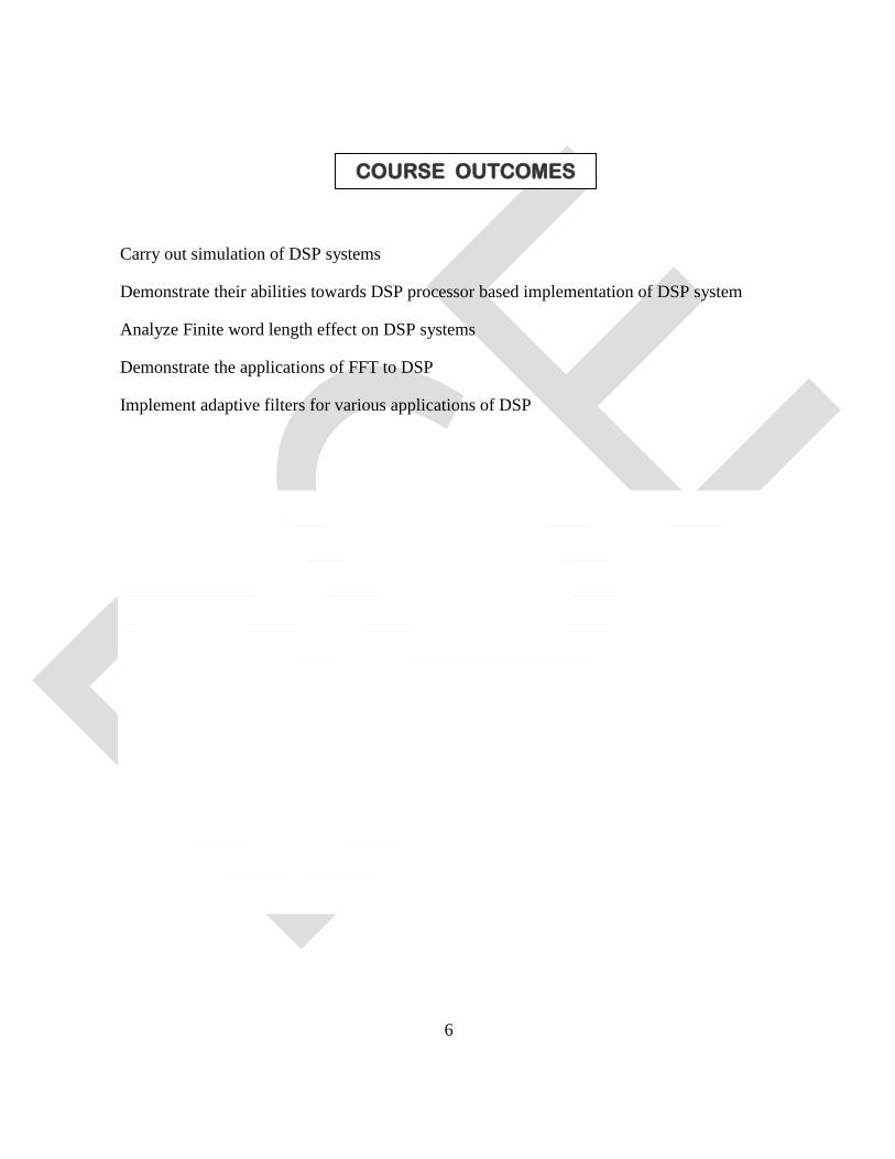
Carry out simulation of DSP systems
Demonstrate their abilities towards DSP processor based implementation of DSP system
Analyze Finite word length effect on DSP systems
Demonstrate the applications of FFT to DSP
Implement adaptive filters for various applications of DSP
COURSE OUTCOMES
7
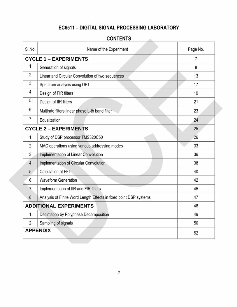
EC6511 – DIGITAL SIGNAL PROCESSING LABORATORY
CONTENTS
Sl.No. Name of the Experiment Page No.
CYCLE 1 – EXPERIMENTS 7
1 Generation of signals 8
2 Linear and Circular Convolution of two sequences 13
3 Spectrum analysis using DFT 17
4 Design of FIR filters 19
5 Design of IIR filters 21
6 Multirate filters linear phase L-th band filter 23
7 Equalization 24
CYCLE 2 – EXPERIMENTS 25
1 Study of DSP processor TMS320C50 26
2 MAC operations using various addressing modes 33
3 Implementation of Linear Convolution 36
4 Implementation of Circular Convolution 38
5 Calculation of FFT 40
6 Waveform Generation 42
7 Implementation of IIR and FIR filters 45
8 Analysis of Finite Word Length Effects in fixed point DSP systems 47
ADDITIONAL EXPERIMENTS 48
1 Decimation by Polyphase Decomposition 49
2 Sampling of signals 50
APPENDIX
52
8
CYCLE 1 - EXPERIMENTS
9
Aim:
To write a program to generate the following sequences and to verify usingMATLAB
• Sinewave
• Cosinewave
• Rampsignal
• Exponentialsignal
• Impulsesignal
• Stepsignal
• Saw toothsignal
• Rectangularsignal
• Randomsequence
• Autocorrelation
• Crosscorrelation
Apparatus Required:
PC with MATLAB software
Algorithm:
Sine WaveGeneration:
1. Start
2. Get the frequency and range oftime‘t’.
3. Determine the values of the sinefunction.
4. Plot the graph for obtained values in continuous and discreteforms.
5. Label the x and yaxes.
6. Stop
Expt. No. 1
GENERATION OF SIGNALS
10
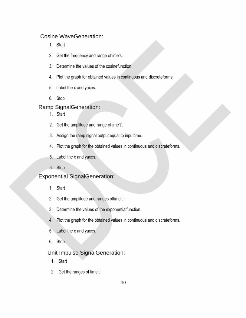
Cosine WaveGeneration:
1. Start
2. Get the frequency and range oftime’s.
3. Determine the values of the cosinefunction.
4. Plot the graph for obtained values in continuous and discreteforms.
5. Label the x and yaxes.
6. Stop
Ramp SignalGeneration:
1. Start
2. Get the amplitude and range oftime‘t’.
3. Assign the ramp signal output equal to inputtime.
4. Plot the graph for the obtained values in continuous and discreteforms.
5. Label the x and yaxes.
6. Stop
Exponential SignalGeneration:
1. Start
2. Get the amplitude and ranges oftime‘t’.
3. Determine the values of the exponentialfunction.
4. Plot the graph for the obtained values in continuous and discreteforms.
5. Label the x and yaxes.
6. Stop
Unit Impulse SignalGeneration:
1. Start
2. Get the ranges of time‘t’.
11
3. Determine the values of the unit impulsesignal.
4. Plot the graph for the obtained values in discreteform.
5. Label the x and yaxes.
6. Stop
Step SignalGeneration:
1. Start
2. Get the amplitude and ranges of time‘t’.
3. Determine the values of the unit stepsignal.
4. Multiply the unit step signal with givenamplitude.
5. Plot the graph for the resultant values in continuous and discreteforms.
6. Label the x and yaxes.
7. Stop
Saw tooth SignalGeneration:
1. Start
2. Get the ranges of time‘t’.
3. Determine the values of the saw toothsignal.
4. Plot the graph for the obtained values in discreteform.
5. Label the x and yaxes.
6. Stop
Rectangular SignalGeneration:
1. Start
2. Get the amplitude and ranges of time‘t’.
3. Determine the values of the rectangularsignal.
4. Multiply the unit step signal with givenamplitude.
12
5. Plot the graph for the resultant values in continuous and discreteforms.
6. Label the x and yaxes.
7. Stop
RandomSequence:
1. Start
2. Get the length of inputsequence.
3. Generate random signals of the specifiedlength
4. Plot the graph for the resultant values in discreteform.
5. Label the x and yaxes.
6. Stop
AutoCorrelation:
1. Start
2. Get the length of input sequence.
3. Generate a rectangular signal of given length.
4. Calculate auto correlation of the rectangular signal.
5. Plot the graph for the resultant values in discrete forms.
6. Label the x and y axes.
7. Stop
CrossCorrelation:
1. Start
2. Get the length of inputsequence.
3. Generate sinusoidal and cosine waveforms of givenlength.
4. Calculate cross correlation of the twosignals.
5. Plot the graph for the resultant values in discreteforms.
6. Label the x and yaxes.
7. Stop
13
Procedure:
Enter the program inworkspace.
1. Save and Run it in .mfiles.
2. Observe the output (waveform) in figurewindow.
Result:
Thus the programs to generate the waveforms were written and outputs were verified using
MATLAB.
1. Define – Impulse Function
2. Define – Unit Step Function
3. What is a ramp function?
4. What is an exponential function?
5. Give the relation among impulse, unit step and rampfunction.
Viva-voce
Aim:
To write a program to perform the following convolutions and to verify usingMATLAB
• Linearconvolution
• Circularconvolution
• Linear convolution using circularconvolution
• Linear convolution usingDFT
• Circular convolution usingDFT
Apparatus Required:
PC with MATLAB software
Algorithm:
LinearConvolution:
1. Start
2. Get the two inputsequences.
3. Obtain the linear convolution of twosequences.
4. Calculate the lengths of inputsequences.
5. Assign the length of resultant sequence(N) equal to length of first sequence(L) + length of
second sequence(M) –1 (N = L+M–1).
6. Plot the input sequences and output sequence in discrete form corresponding to
theirlengths.
7. Label the x and yaxes.
8. Display the resultant sequencevalues.
9. Stop
Expt. No. 2 LINEAR AND CIRCULAR CONVOLUTION OF
TWO SEQUENCES
1
CircularConvolution:
1. Start
2. Get the two inputsequences.
3. Check the maximum length (N) of twosequences.
4. By zero padding, make both the two sequences with equal length(N).
5. Calculate circular convolution of equal lengthsequences.
6. Plot the input sequences and output sequence in discrete form corresponding to theirlengths.
7. Label the x and yaxes.
8. Display the resultant sequencevalues.
9. Stop
Linear Convolution using CircularConvolution:
1. Start
2. Get the two input sequences.
3. Calculate the lengths of input sequences.
4. Assign the length of resultant sequence(N) equal to length of first sequence(L)+
length of second sequence(M) – 1 (N=L+M-1)
5. By zero padding, make both the two sequences with equal length (N).
6. Obtain the circular convolution of two sequences.
7. Plot the input sequences and output sequence in discrete form corresponding to
their lengths.
8. Label the x and y axes.
9. Display the resultant sequence values.
10. Stop
2
Linear Convolution using DFTmethod:
1. Start.
2. Get the two input sequences.
3. Calculate the lengths of input sequences.
4. Assign the length of resultant sequence(N) equal to length of first sequence(L) +b length of
second sequence(M) – 1 (N=L+M-1)
5. By zero padding, make both the two sequences with equal length (N).
6. Calculate the N-point FFT of two sequences.
7. Multiply the two FFTs.
8. Calculate the N-point IFFT of the sequence.
9. Plot the input sequences and output sequences FFT and IFFT in discrete form
corresponding to their lengths.
10. Label the x and y axes.
11. Display the resultant sequence values.
12. Stop.
Circular Convolution using DFTmethod:
1. Start
2. Get the two input sequences.
3. Calculate the lengths of input sequences.
4. Check the maximum length (N) of two sequences.
5. By zero padding, make both the two sequences with equal length (N).
6. Calculate the N-point FFT of two sequences.
7. Multiply the two FFTs.
3
8. Calculate the N-point IFFT of the sequence.
9. Plot the input sequences and output sequences FFT and IFFT in discrete form
corresponding to theirlengths.
10. Label the x and yaxes.
11. Display the resultant sequence values.
12. Stop.
Procedure:
1. Enter the program inworkspace.
2. Save and Run it in. m files.
3. Observe the output in command window and in figure window.
Result:
Thus the linear and circular convolution of the given two sequences was obtained using
MATLAB.
1. What is the length of the linearly convolved signal?
2. What is the difference between linear convolution and
circular convolution?
3. What are the different methods of linear convolution?
4. How will you obtain linear convolution using circular
convolution?
5. What is meant by Zero Padding?
6. What is the length of the circularly convolved signal?
Viva-voce
Aim:
To write a program to analyze the spectrum of a signal using Discrete Fourier Transform
(DFT) and Fast Fourier Transform (FFT) using MATLAB
Apparatus Required:
PC with MATLAB software
Algorithm:
1. Start
2. Get the inputsequence.
3. Obtain the DFT of inputsequence.
4. Find the magnitude and phase response of theDFT.
5. Plot the magnitude and phase in continuous and in discrete forms.
6. Stop
PROCEDURE:
1. Enter the program inworkspace.
2. Save and Run it in .mfiles.
3. Observe the output in command window or in figurewindow.
Result:
Thus the program to analyze the spectrum of a signal using Discrete Fourier Transform
(DFT) is verified using MATLAB.
Expt. No. 3 SPECTRUM ANALYSIS USING DFT
1
1. Differentiate DIT from DIF algorithm.
2. How many multiplication terms are required for doing DFT
by expressional method and FFT method?
3. How many stages are there for 8 point DFT?
4. What is the inverse DFT of X(k) = {3,4,5,6}?
Viva-voce
Aim:
To write a program to design and obtain the magnitude and phase responses for the given
FIR filter using MATLAB.
Apparatus Required:
PC with MATLAB software
Algorithm:
1. Start
2. Get the values of pass band and stop bandripples.
3. Get the values of sampling, pass band and stop bandfrequencies.
4. Select the type of the FIRfilter.
5. Find the order of thefilter.
6. Obtain the filterco-efficient.
7. Find the magnitude and phase responses of thefilter.
8. Plot the magnitude and phaseresponses.
9. Stop
Procedure:
1. Enter the program inworkspace.
2. Save and Run it in .mfiles.
3. Observe the output in figurewindow.
Expt. No. 4 DESIGN OF FIR FILTERS
1
Result:
Thus the program for the given FIR filter was written and its magnitude and phase
responses were verified.
1. What is meant by filter?
2. What is the difference between analog and digital filter?
3. What are the specifications required to design filter?
4. What is meant by FIR filter?
5. List the well known design technique for linear phase FIR filter design?
Viva-voce
2
Aim:
To write a program to design and obtain the response of the given IIR filter usingMATLAB
Apparatus Required:
PC with MATLAB software
Algorithm:
1. Start
2. Get the values of pass band and stop bandripples
3. Get the values of sampling, pass band and stop bandfrequencies.
4. Select the type of the IIRfilter.
5. Find the order of thefilter.
6. Obtain the filter transferfunction.
7. Find the magnitude and phase responses of thefilter.
8. Plot the magnitude and phaseresponses.
9. Stop
Procedure:
1. Enter the program inworkspace.
2. Save and Run it in .mfiles.
3. Observe the output in figurewindow.
Expt. No. 5 DESIGN OF IIR FILTERS
3
RESULT:
Thus the program for IIR filter was written and its magnitude and phase responses were
verified.
1. Define – IIR Filter
2. How digital filter is designed using impulse invariant method?
3. What are the disadvantages of impulse invariant method?
4. Distinguish IIR and FIR filters.
5. Write the expression for order State the steps to design digital IIR filter using bilinear
method of Butterworth filter?
Viva-voce
4
Aim
To design linear-phase FIR Lth-band filters of the length N =31, with L = 3 and with the roll-off
factors: ρ = 0.2, 0.4, and 0.6. Plot the impulse responses and the magnitude responses for all designs
Apparatus Required:
PC with MATLAB software
Procedure:
1. Enter the program inworkspace.
2. Save and Run it in .mfiles.
3. Observe the output in command window or in figurewindow.
Result:
Thus the programs for multirate filters were verified using MATLAB.
Expt. No. 6 MULTIRATE FILTERS LINEAR PHASE L – TH BAND FILTER
1. Define – Interpolation
2. Define – Decimation
3. How to improve computational efficiency of FIR filters using interpolators?
4. How to avoid aliasing at the output in the decimation process?
5. What are the filter banks withcomplementary frequency response?
Viva-voce
5
Aim To write MATLAB program to design adaptive channel equalization using LMS algorithm
Apparatus Required:
PC with MATLAB software
Result:
Thus the adaptive channel equalization is designed using LMS algorithm and the output is
obtained using MATLAB.
Expt. No. 7 EQUALIZATION
1. What is meant by Adaptive Equalization?
2. What is meant by LMS?
3. What is meant by Decision Directed Mode?
4. What are the two steps in the process of Adaptive equalization?
Viva-voce
6
CYCLE 2 - EXPERIMENTS
7
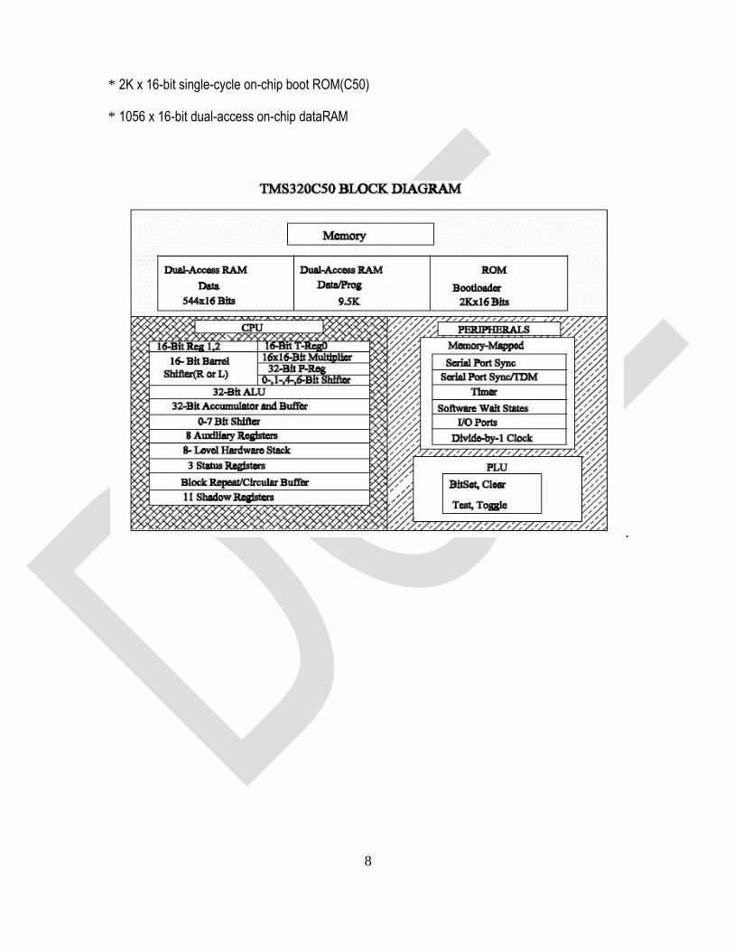
Aim:
To study the architecture overview of DSP processor TMS320C50
Introduction:
It is needless to say that in order to utilize the full feature of the DSP chip TMS320C50, the
DSP engineer must have a complete knowledge of the DSP device. This chapter is an introduction
to the hardware aspects of the TMS320C50. The important units of TMS320C50 arediscussed.
The DSP Chip Tms320c50:
The TMS320C50 is a 16-bit fixed point digital signal processor that combines the flexibility
of a high speed controller with the numerical capability of an array processor, thereby offering an
inexpensive alternative to multichip bit-slice processors. The highly paralleled architecture and
efficient instruction set, provide speed and flexibility capable of executing 10 MIPS (Million
Instructions Per Second). The TMS320C50 optimizes speed by implementing functions in
hardware that other processors implement through microcode or software. This hardware intensive
approach provides the design engineer with processing power previously unavailable on a single
chip.
The TMS320C50 is the third generation digital signal processor in the TMS320 family. Its
powerful instruction set, inherent flexibility, high-speed number-crunching capabilities, and
innovative architecture have made this high-performance, cost-effective processor the ideal
solution to many telecommunications, computer, commercial, industrial, and military applications.
Key Features of TMS320C50:
The key features of the Digital Signal Processor TMS320C50 are:
* 35-/50-ns single-cycle fixed-point instruction execution time (28.6/20MIPS)
* Upward source-code compatible with all C1X and C2xdevices
* RAM-based memory operation(C50)
* 9K x 16-bit single-cycle on-chip program/data RAM(C50)
Expt. No. 8 STUDY OF DSP PROCESSOR TMS320C50
8
* 2K x 16-bit single-cycle on-chip boot ROM(C50)
* 1056 x 16-bit dual-access on-chip dataRAM
.
9
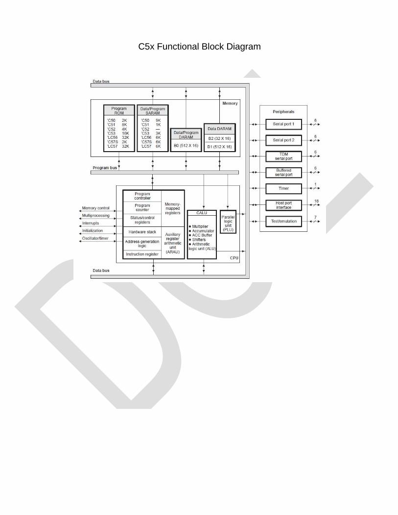
C5x Functional Block Diagram
10
* 224K x 16-bit maximum addressable external memory space (64K program, 64K data, 64K I/O,
and 32Kglobal)
* 32-bit arithmetic logic unit (ALU), 32-bit accumulator (ACC), and 32-bit accumulator buffer
(ACCB)
* 16-bit parallel logic unit(PLU)
* 16 x 16-bit parallel multiplier with a 32-bit productcapability.
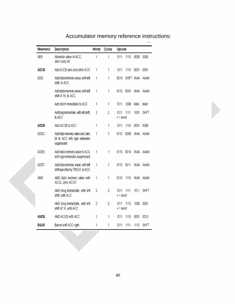
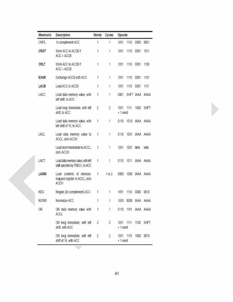
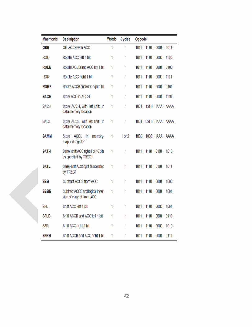
* Single-cycle multiply/accumulateinstructions
* Eight auxiliary registers with a dedicated auxiliary register arithmetic unit for indirect