Page 1
1
Diagonal 7.81 mm (Type 1/2.3) CMOS Image Sensor with Square Pixel for Color
Cameras
IMX172LQT-C
Description
The IMX172 LQT-C is a diagonal 7.81 mm (Type 1/2.3) CMOS image sensor with a color square pixel array and
approximately 12.4M effective pixels. The image sensor can output effective approximately 9.03M pixels signal for
high-definition (4K2K:4096 × 2160) moving picture at 59.94 frame/s in 10-bit-digital output format.
In addition, sensor supporting horizontal/vertical addition, this is capable of outputting a 12 bit digital for HD1080
(2048 × 1080) -60p moving picture. For still picture imaging, this sensor can output approximately 12.4 M effective
pixels signal in a high-definition 12-bit digital output format. Realizing high-sensitivity, low dark current, this sensor
also has an electronic shutter function with variable storage time.
Applications: Industrial cameras (use for TV conference, FA, Security)
Features
◆ CMOS active pixel type pixels
◆ Input clock frequency 72 MHz
◆ Number of effective pixels (12M) : 4072 (H) x3046 (V) approx 12.4M pixels
◆ Number of effective pixels (4K2K) : 4152 (H) x2174 (V) approx 9.03M pixels
◆ Readout mode
All-pixel scan mode (12 M, 4K2K)
Horizontal/vertical 2/2-line binning mode (4K2K)
◆ High-sensitivity, low dark current, no smear, excellent anti-blooming characteristics
◆ Variable-speed shutter function (minimum unit: 1 horizontal sync signal period (1XHS))
◆ Low power consumption
◆ H driver, V driver and serial communication circuit on chip
◆ CDS/PGA on chip. Gain +27 dB (step pitch < 0.1 dB)
◆ 10-bit/12-bit A/D conversion on chip
◆ R, G, B primary color mosaic filters on chip
Sony reserves the right to change products and specifications without prior notice.
This information does not convey any license by any implication or otherwise under any patents or other right.
Application circuits shown, if any, are typical examples illustrating the operation of the devices. Sony cannot assume responsibility for
any problems arising out of the use of these circuits.
FRAMOS G
MBH
Page 2
IMX172LQT-C
2
Device Structure
◆ CMOS image sensor
◆ Image size
Diagonal 7.81 mm (Type 1/2.3)
◆ Total number of pixels
4168 (H) × 3062 (V) approx. 12.76 M pixels
◆ Number of effective pixels
- Type 1/2.3 (12M) : 4072 (H) × 3046 (V) approx. 12.40 M pixels
- Type 1/2.5 (4K2K) : 4152 (H) × 2174 (V) approx. 9.03 M pixels
◆ Number of active pixels
- Type 1/2.3 (12M) : 4024 (H) × 3036 (V) approx. 12.22 M pixels diagonal 7.81 mm
- Type 1/2.5 (4K2K) : 4120 (H) × 2168 (V) approx. 8.93 M pixels diagonal 7.22 mm
◆ Number of recommended recording pixels
- Type 1/2.3 (12M) : 4000 (H) × 3000 (V) 12.00 M pixels aspect ratio 4:3
- Type 1/2.5 (4K2K) : 4096 (H) × 2160 (V) approx. 8.85 M pixels aspect ratio approx. 17:9
◆ Chip size
8.998 mm (H) × 7.556 mm (V)
◆ Unit cell size
1.55 μm (H) × 1.55 μm (V)
◆ Optical black
Horizontal (H) direction : Front 96 pixels, rear 0 pixel
Vertical (V) direction : Front 16 pixels, rear 0 pixel
◆ Substrate material
Silicon
Optical Black Array and Readout Scan Direction
(Top View)
H
V
L1
01A01L
A1 (1Pin)
Note) Arrows in the figure indicate scanning direction during normal readout in the vertical direction.
FRAMOS G
MBH
Page 3
IMX172LQT-C
3
Absolute Maximum Ratings
◆ Supply voltage 1 VADD*1
–0.3 to +3.3 V
◆ Supply voltage 2 VDDD1*2
–0.5 to +2.0 V
◆ Supply voltage 3 VDDD2 *3
–0.5 to +3.3 V
◆ Input voltage (digital) VI –0.3 to VDDD2 + 0.3 V
◆ Output voltage (digital) VO –0.3 to VDDD2 + 0.3 V
◆ Guaranteed operating temperature TOPR –10 to +75 °C
◆ Storage guarantee temperature TSTG –30 to +80 °C
◆ Performance guarantee temperature TSPEC –10 to +60 °C
Recommended Operating Conditions
◆ Supply voltage 1 VADD*1
2.8 ± 0.1 V
◆ Supply voltage 2 VDDD1*2
1.2 ± 0.1 V
◆ Supply voltage 3 VDDD2*3
1.8 ± 0.1 V
◆ Input voltage (digital) VI –0.1 to VDDD2 + 0.1 V
◆ Output voltage (digital) VO –0.1 to VDDD2 + 0.1 V
*1
VADD : VDDSUB, VDDHCM, VDDHVS, VDDHPX, VDDHDA, VDDHCP (2.8 V power supply) *2
VDDD1 : VDDLCN1 and VDDLCN2, VDDLSC1 and VDDLSC2, VDDLPL (1.2 V power supply) *3
VDDD2 : VDDMIO, VDDMLV1 and VDDMLV2 (1.8 V power supply)
FRAMOS G
MBH
Page 4
IMX172LQT-C
4
USE RESTRICTION NOTICE
This USE RESTRICTION NOTICE ("Notice") is for customers who are considering or currently using the
image sensor products ("Products") set forth in this specifications book. Sony Corporation ("Sony") may,
at any time, modify this Notice which will be available to you in the latest specifications book for the
Products. You should abide by the latest version of this Notice. If a Sony subsidiary or distributor has its
own use restriction notice on the Products, such a use restriction notice will additionally apply between
you and the subsidiary or distributor. You should consult a sales representative of the subsidiary or
distributor of Sony on such a use restriction notice when you consider using the Products.
Use Restrictions
The Products are intended for incorporation into such general electronic equipment as office products,
communication products, measurement products, and home electronics products in accordance with
the terms and conditions set forth in this specifications book and otherwise notified by Sony from time
to time.
You should not use the Products for critical applications which may pose a life- or injury-threatening
risk or are highly likely to cause significant property damage in the event of failure of the Products. You
should consult your sales representative beforehand when you consider using the Products for such
critical applications. In addition, you should not use the Products in weapon or military equipment.
Sony disclaims and does not assume any liability and damages arising out of misuse, improper use,
modification, use of the Products for the above-mentioned critical applications, weapon and military
equipment, or any deviation from the requirements set forth in this specifications book.
Design for Safety
Sony is making continuous efforts to further improve the quality and reliability of the Products; however,
failure of a certain percentage of the Products is inevitable. Therefore, you should take sufficient care
to ensure the safe design of your products such as component redundancy, anti-conflagration features,
and features to prevent mis-operation in order to avoid accidents resulting in injury or death, fire or
other social damage as a result of such failure.
Export Control
If the Products are controlled items under the export control laws or regulations of various countries,
approval may be required for the export of the Products under the said laws or regulations.
You should be responsible for compliance with the said laws or regulations.
No License Implied
The technical information shown in this specifications book is for your reference purposes only. The
availability of this specifications book shall not be construed as giving any indication that Sony and its
licensors will license any intellectual property rights in such information by any implication or otherwise.
Sony will not assume responsibility for any problems in connection with your use of such information or
for any infringement of third-party rights due to the same. It is therefore your sole legal and financial
responsibility to resolve any such problems and infringement.
Governing Law
This Notice shall be governed by and construed in accordance with the laws of Japan, without reference
to principles of conflict of laws or choice of laws. All controversies and disputes arising out of or relating
to this Notice shall be submitted to the exclusive jurisdiction of the Tokyo District Court in Japan as the
court of first instance.
Other Applicable Terms and Conditions
The terms and conditions in the Sony additional specifications, which will be made available to you when
you order the Products, shall also be applicable to your use of the Products as well as to this
specifications book. You should review those terms and conditions when you consider purchasing
and/or using the Products.
FRAMOS G
MBH
Page 5
IMX172LQT-C
5
Contents
Description ......................................................................................................................................................................1
Features ..........................................................................................................................................................................1
Device Structure ..............................................................................................................................................................2
Optical Black Array and Readout Scan Direction ...............................................................................................................2
Absolute Maximum Ratings ..............................................................................................................................................3
Recommended Operating Conditions ...............................................................................................................................3
USE RESTRICTION NOTICE ..........................................................................................................................................4
Chip Center and Optical Center ........................................................................................................................................7
Pin Configuration .............................................................................................................................................................8
Pin Description ................................................................................................................................................................9
Electrical Characteristics ................................................................................................................................................ 12
1. DC Characteristics.................................................................................................................................................. 12
2. AC Characteristics .................................................................................................................................................. 14
3. LVDS output ........................................................................................................................................................... 16
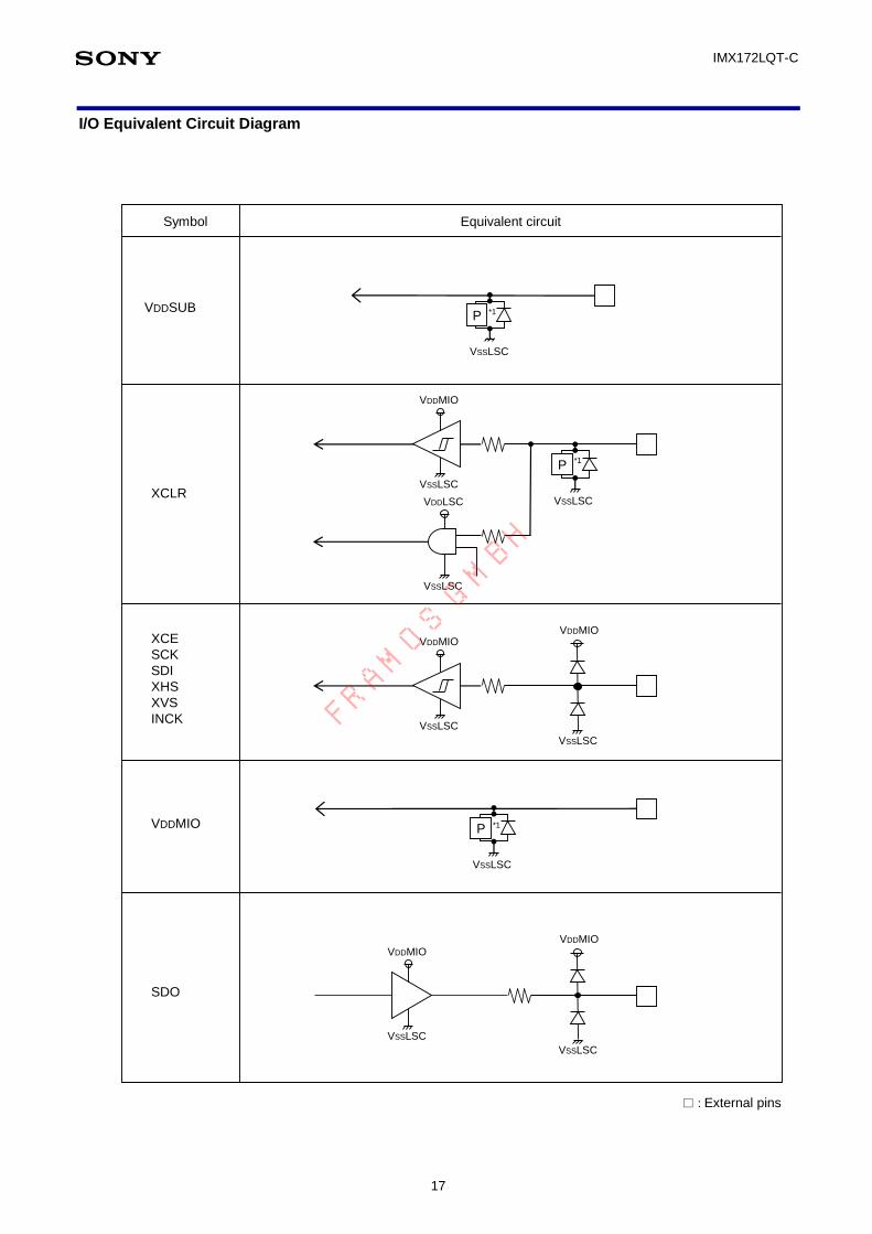
I/O Equivalent Circuit Diagram ....................................................................................................................................... 17
Spectral Sensitivity Characteristics ................................................................................................................................. 22
Image Sensor Characteristics ........................................................................................................................................ 23
1. Zone Definition of Video Signal Shading .................................................................................................................. 23
Image Sensor Characteristics Measurement Method ...................................................................................................... 24
1. Measurement Conditions ........................................................................................................................................ 24
2. Color Coding of this Image Sensor and Readout ..................................................................................................... 24
3. Definition of Standard Imaging Conditions ............................................................................................................... 24
Setting Registers by Serial Communication .................................................................................................................... 26
Register Map ................................................................................................................................................................. 27
1. Register Value Reflection Timing to Output Data ...................................................................................................... 31
2. Description of Register ........................................................................................................................................... 32
3. Register Setting for Each Readout Drive Mode ........................................................................................................ 40
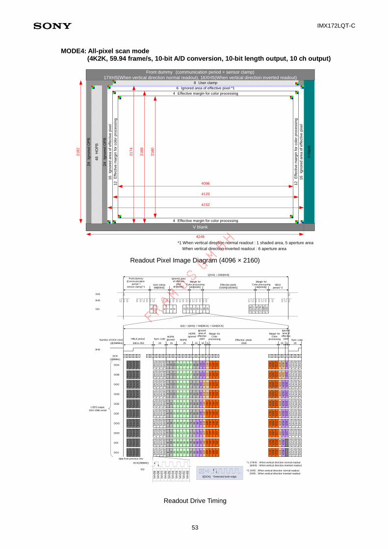
Readout Drive Modes .................................................................................................................................................... 42
1. Readout Drive Modes ............................................................................................................................................. 42
1-1. Description of Readout Drive Modes ................................................................................................................. 42
1-2. Relationship between Arithmetic Processing and the Number of Output Bits in Each Readout Drive Mode .......... 43
2. Sync Signals and Data Output Timing ..................................................................................................................... 44
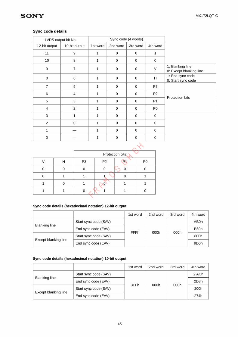
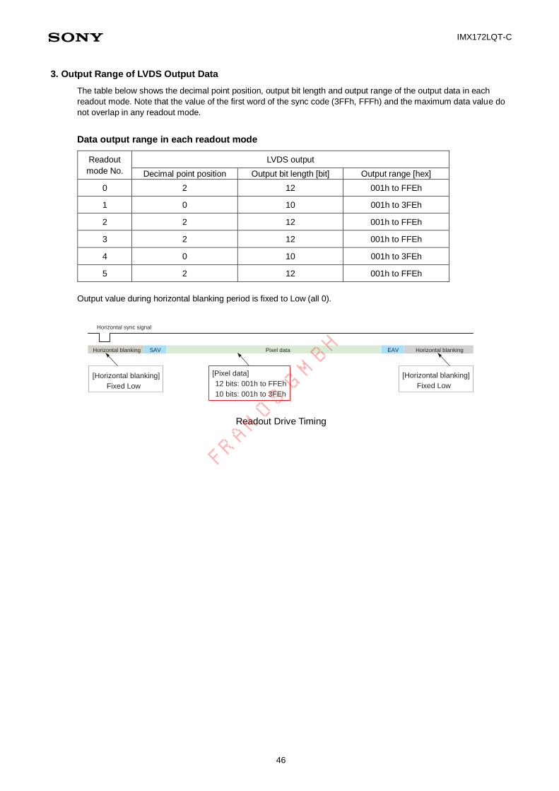
3. Output Range of LVDS Output Data ........................................................................................................................ 46
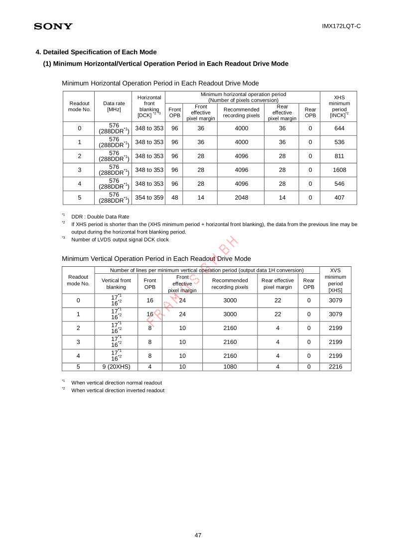
4. Detailed Specification of Each Mode ....................................................................................................................... 47
(1) Minimum Horizontal/Vertical Operation Period in Each Readout Drive Mode ........................................................ 47
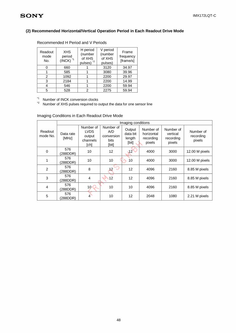
(2) Recommended Horizontal/Vertical Operation Period in Each Readout Drive Mode............................................... 48
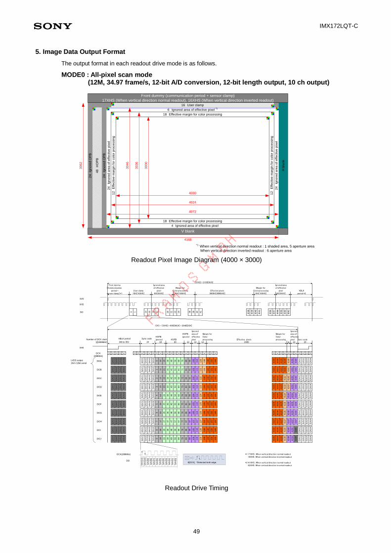
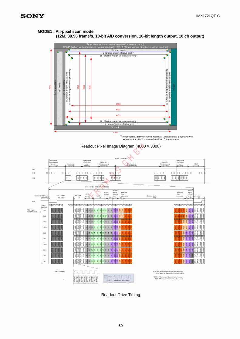
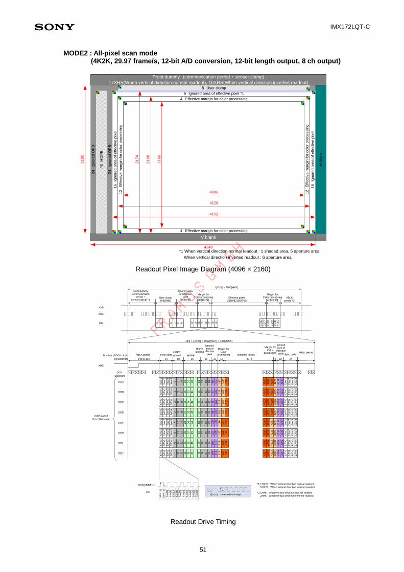
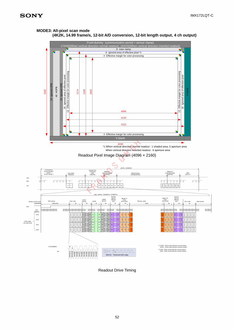
5. Image Data Output Format ..................................................................................................................................... 49
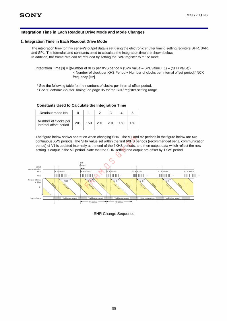
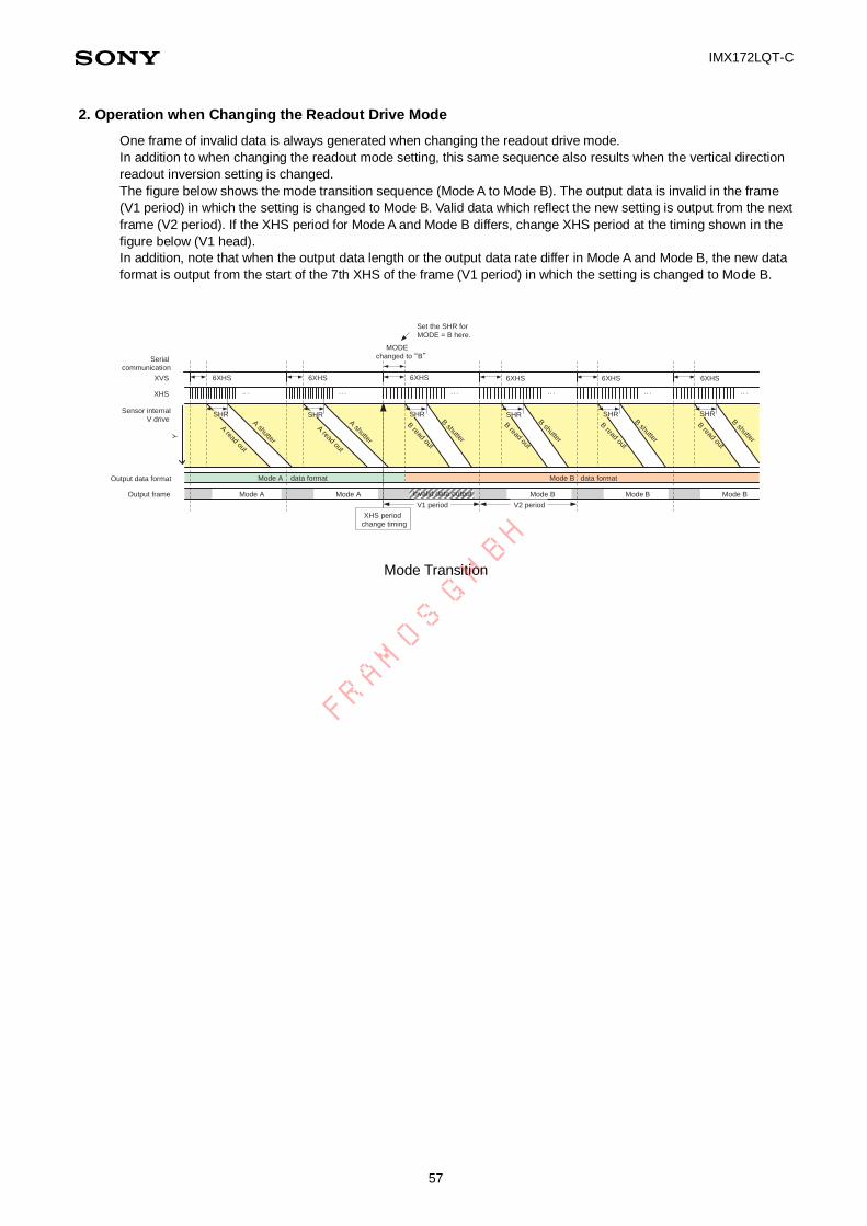
Integration Time in Each Readout Drive Mode and Mode Changes.................................................................................. 55
1. Integration Time in Each Readout Drive Mode ......................................................................................................... 55
2. Operation when Changing the Readout Drive Mode ................................................................................................ 57
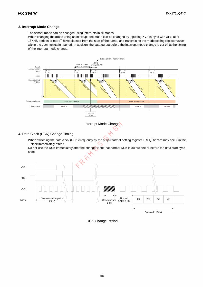
3. Interrupt Mode Change ........................................................................................................................................... 58
4. Data Clock (DCK) Change Timing ........................................................................................................................... 58
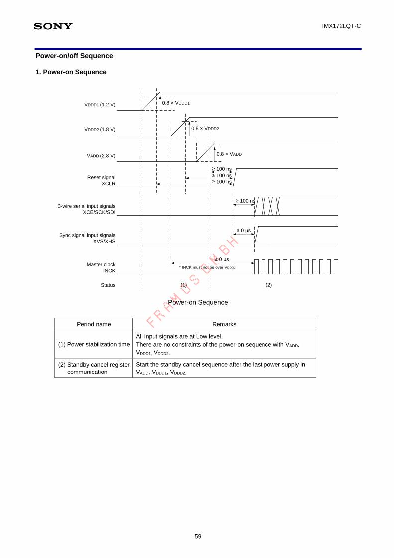
Power-on/off Sequence .................................................................................................................................................. 59
1. Power-on Sequence ............................................................................................................................................... 59
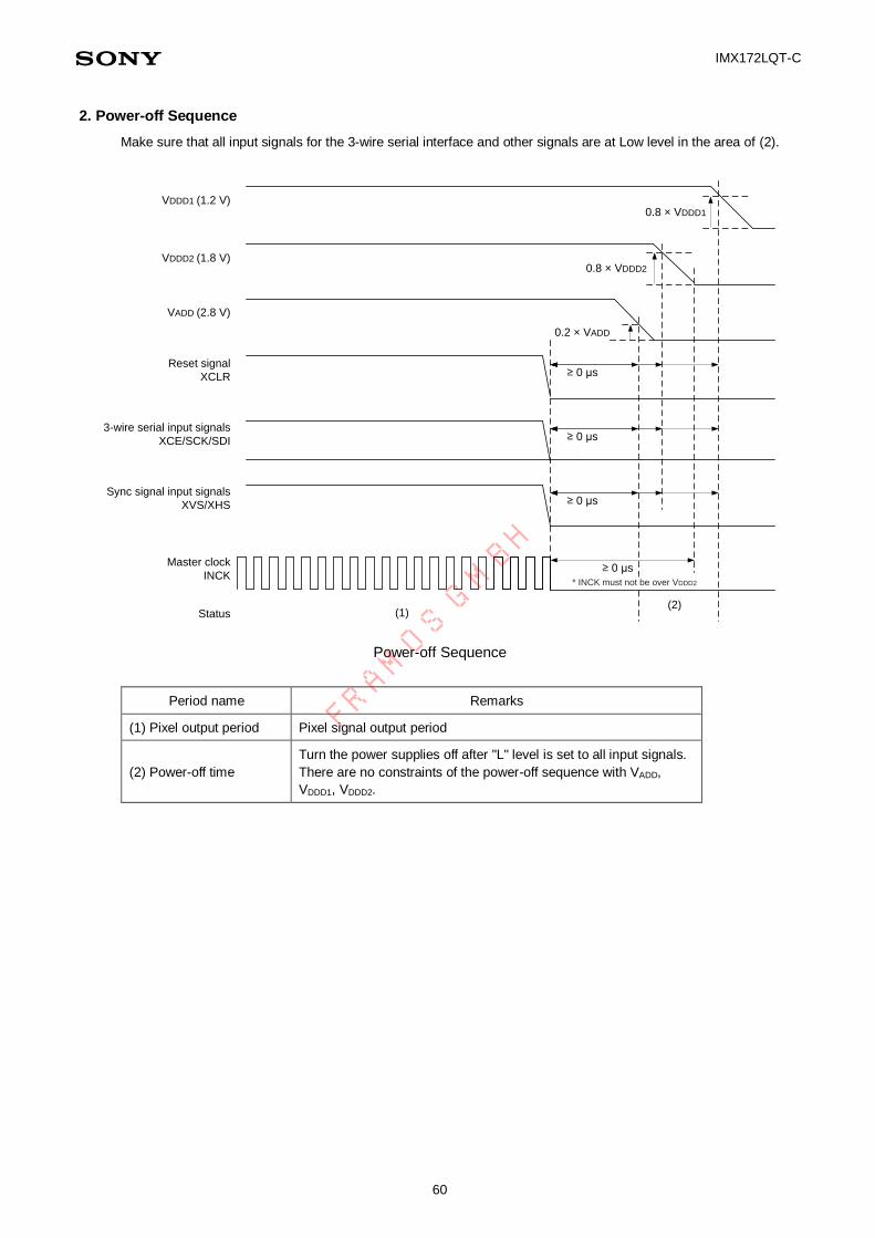
2. Power-off Sequence ............................................................................................................................................... 60
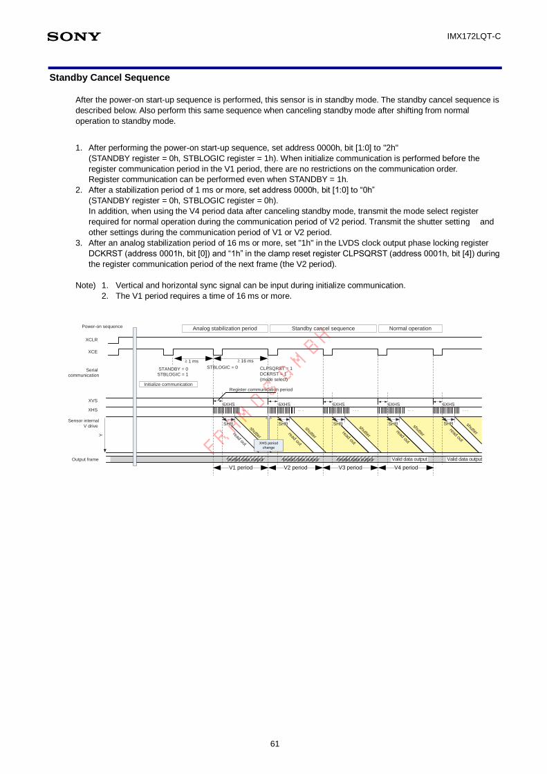
Standby Cancel Sequence ............................................................................................................................................. 61
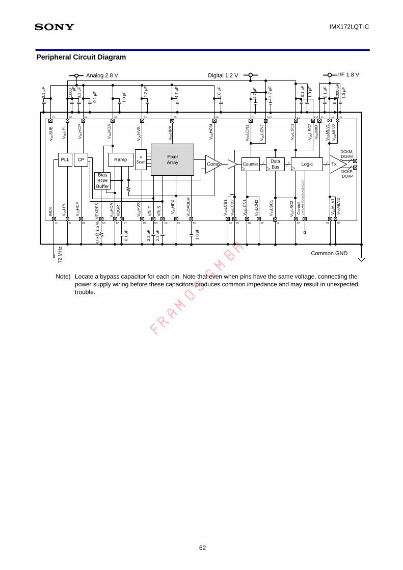
Peripheral Circuit Diagram ............................................................................................................................................. 62
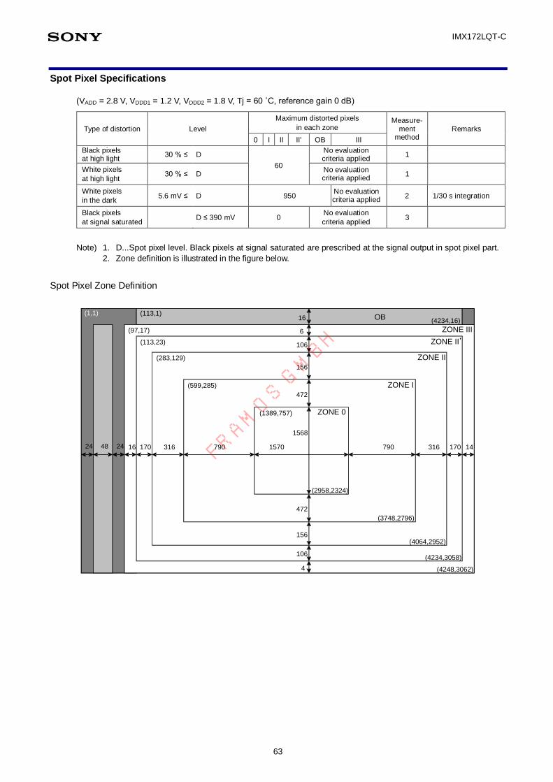
Spot Pixel Specifications ................................................................................................................................................ 63
Spot Pixel Zone Definition........................................................................................................................................... 63
Notice on White Pixels Specifications ............................................................................................................................. 64
FRAMOS G
MBH
Page 6
IMX172LQT-C
6
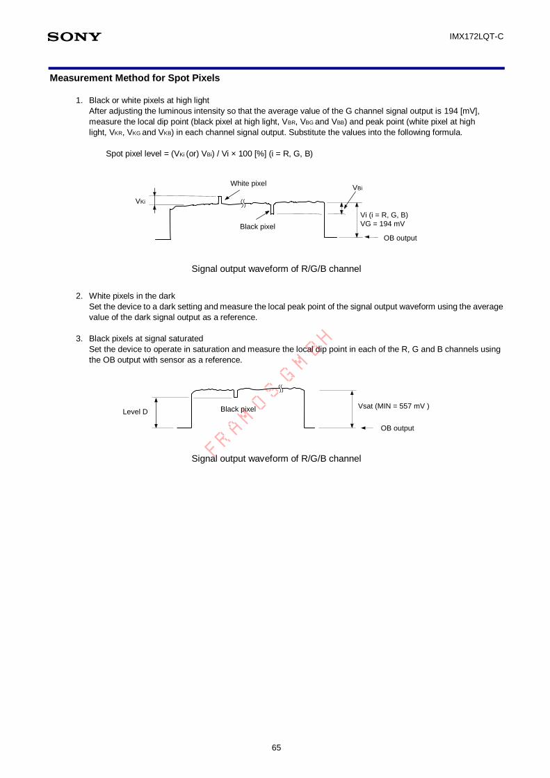
Measurement Method for Spot Pixels ............................................................................................................................. 65
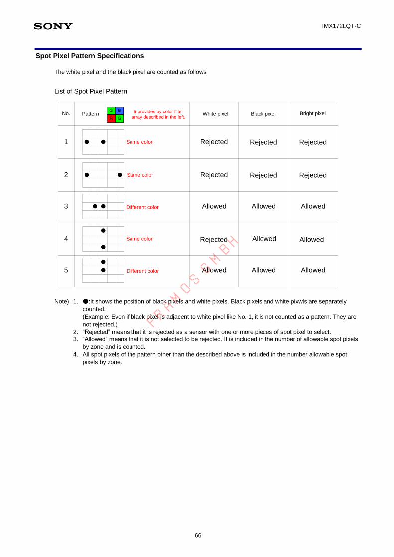
Spot Pixel Pattern Specifications .................................................................................................................................... 66
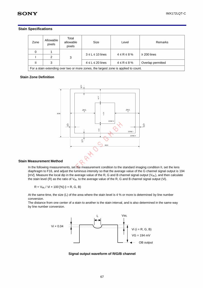
Stain Specifications ....................................................................................................................................................... 67
Stain Zone Definition .................................................................................................................................................. 67
Stain Measurement Method ........................................................................................................................................ 67
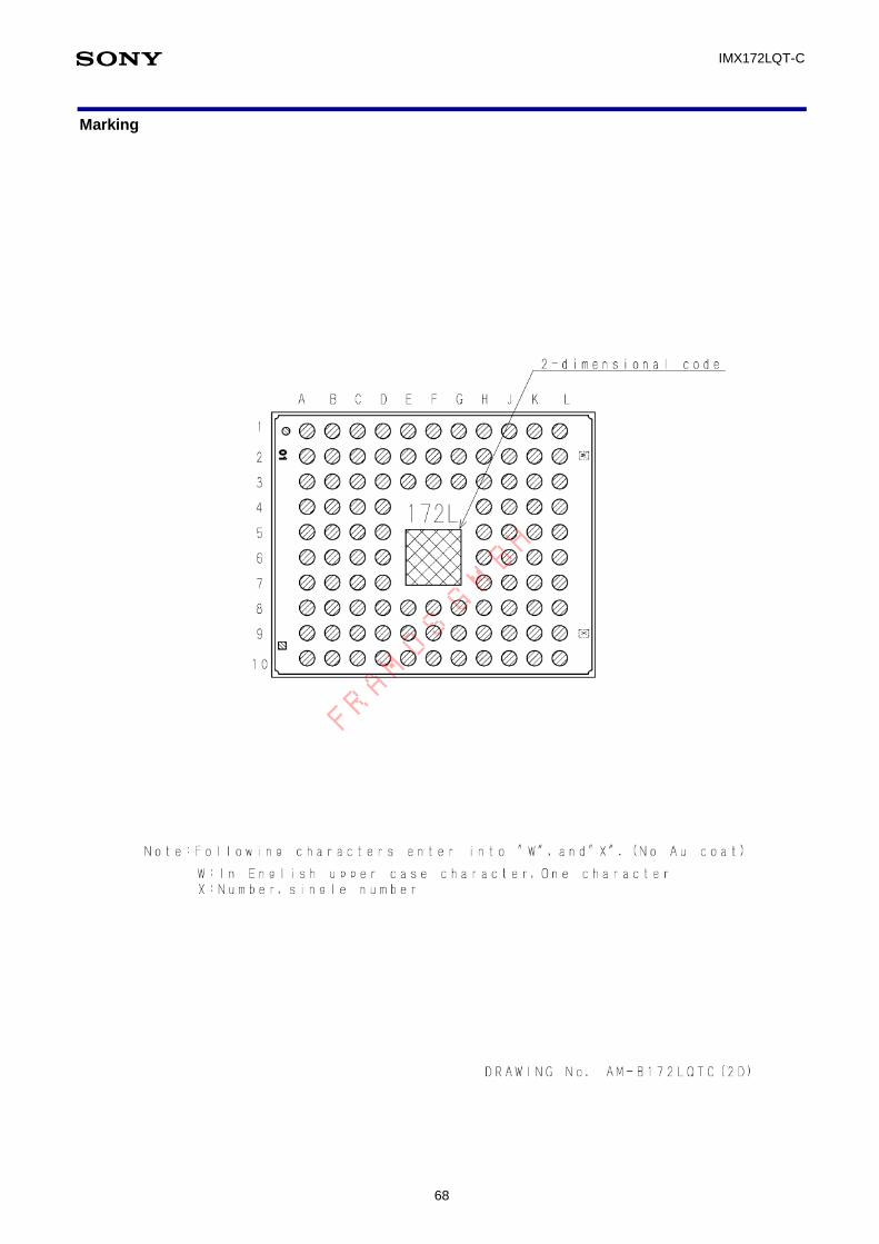
Marking ......................................................................................................................................................................... 68
Notes On Handling ........................................................................................................................................................ 69
Package Outline ............................................................................................................................................................ 71
List of Trademark Logos and Definition Statements ......................................................................................................... 72
FRAMOS G
MBH
Page 7
IMX172LQT-C
7
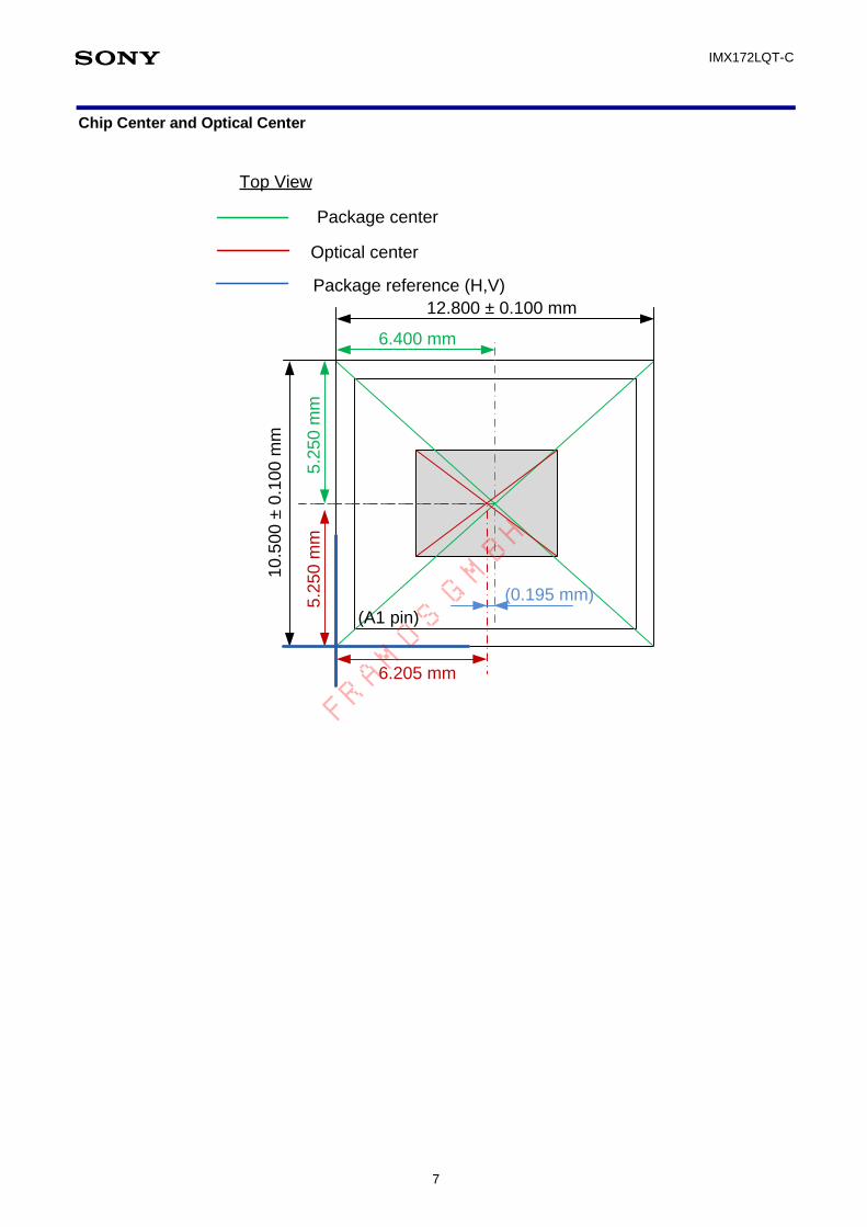
Chip Center and Optical Center
12.800 ± 0.100 mm
10
.50
0 ±
0.1
00
mm
6.400 mm
5.2
50
mm
6.205 mm
5.2
50
mm
Top View
Package center
Optical center
Package reference (H,V)
(A1 pin)
(0.195 mm)
FRAMOS G
MBH
Page 8
IMX172LQT-C
8
Pin Configuration
(Bottom View)
NC
NC
NC
NC
NC
NC NC
NC
NC NC
NC
NC NCNCNC
NC NC NC NC
NC
NC NC NC NC NC NC NC
2
3
4
5
6
7
8
9
1
10
VDDSUB VDDLCN1 VDDLSC1
VDDLPL VSSLPLSCK XVSVSSLCB1 VSSLCN1 VSSLSC1
VDDMIO XCE XHS NC
VDDHVS VSSHVS VRLS XCLR SDISDO DOBMNC DOBP
NC
DOAM
VDDHCP VSSHCP VRLT NC
VSSMLV2
DOEP DOCP DOCM
VDDHPX VLOADLM NC NC
VSSMLV1
DOEM DODP DODM
VDDHCM VSSHPX VEXRES
VDDMLV2
DCKP DOFP DOFM
VDDHDA VSSHDA VBGR
NC
VDDMLV1
DCKM DOGP DOGM
NC NC NC
NC
NC NCNC DOHP DOHM DOJP DOJM
VSSLCN2 VSSLSC2 NC NC DOIP DOIM
NC VDDLCN2 VDDLSC2 NC NC NC NC
TEST2TEST3
TEST1
DOAP
NC
INCK
NC NC
NC
VSSLCB2
NC
NC
TEST4TEST5
NCNC
NC
NC
NC NC
NC
NC
LKJHGFEDCBA
1pin index
FRAMOS G
MBH
Page 9
IMX172LQT-C
9
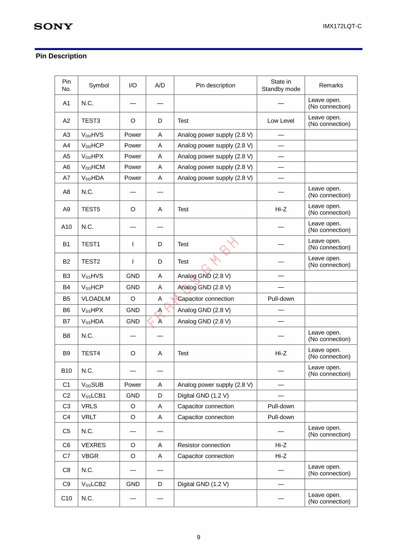
Pin Description
Pin
No. Symbol I/O A/D Pin description
State in
Standby mode Remarks
A1 N.C. — — — Leave open. (No connection)
A2 TEST3 O D Test Low Level Leave open. (No connection)
A3 VDDHVS Power A Analog power supply (2.8 V) —
A4 VDDHCP Power A Analog power supply (2.8 V) —
A5 VDDHPX Power A Analog power supply (2.8 V) —
A6 VDDHCM Power A Analog power supply (2.8 V) —
A7 VDDHDA Power A Analog power supply (2.8 V) —
A8 N.C. — — — Leave open. (No connection)
A9 TEST5 O A Test Hi-Z Leave open. (No connection)
A10 N.C. — — — Leave open. (No connection)
B1 TEST1 I D Test — Leave open. (No connection)
B2 TEST2 I D Test — Leave open. (No connection)
B3 VSSHVS GND A Analog GND (2.8 V) —
B4 VSSHCP GND A Analog GND (2.8 V) —
B5 VLOADLM O A Capacitor connection Pull-down
B6 VSSHPX GND A Analog GND (2.8 V) —
B7 VSSHDA GND A Analog GND (2.8 V) —
B8 N.C. — — — Leave open. (No connection)
B9 TEST4 O A Test Hi-Z Leave open. (No connection)
B10 N.C. — — — Leave open. (No connection)
C1 VDDSUB Power A Analog power supply (2.8 V) —
C2 VSSLCB1 GND D Digital GND (1.2 V) —
C3 VRLS O A Capacitor connection Pull-down
C4 VRLT O A Capacitor connection Pull-down
C5 N.C. — — — Leave open. (No connection)
C6 VEXRES O A Resistor connection Hi-Z
C7 VBGR O A Capacitor connection Hi-Z
C8 N.C. — — — Leave open. (No connection)
C9 VSSLCB2 GND D Digital GND (1.2 V) —
C10 N.C. — — — Leave open. (No connection)
FRAMOS G
MBH
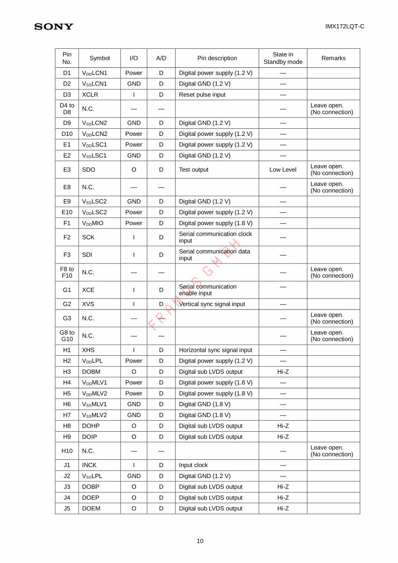
Page 10
IMX172LQT-C
10
Pin
No. Symbol I/O A/D Pin description
State in
Standby mode Remarks
D1 VDDLCN1 Power D Digital power supply (1.2 V) —
D2 VSSLCN1 GND D Digital GND (1.2 V) —
D3 XCLR I D Reset pulse input —
D4 to D8
N.C. — — — Leave open. (No connection)
D9 VSSLCN2 GND D Digital GND (1.2 V) —
D10 VDDLCN2 Power D Digital power supply (1.2 V) —
E1 VDDLSC1 Power D Digital power supply (1.2 V) —
E2 VSSLSC1 GND D Digital GND (1.2 V) —
E3 SDO O D Test output Low Level Leave open. (No connection)
E8 N.C. — — — Leave open. (No connection)
E9 VSSLSC2 GND D Digital GND (1.2 V) —
E10 VDDLSC2 Power D Digital power supply (1.2 V) —
F1 VDDMIO Power D Digital power supply (1.8 V) —
F2 SCK I D Serial communication clock input
—
F3 SDI I D Serial communication data input
—
F8 to F10
N.C. — — — Leave open. (No connection)
G1 XCE I D Serial communication enable input
—
G2 XVS I D Vertical sync signal input —
G3 N.C. — — — Leave open. (No connection)
G8 to G10
N.C. — — — Leave open. (No connection)
H1 XHS I D Horizontal sync signal input —
H2 VDDLPL Power D Digital power supply (1.2 V) —
H3 DOBM O D Digital sub LVDS output Hi-Z
H4 VDDMLV1 Power D Digital power supply (1.8 V) —
H5 VDDMLV2 Power D Digital power supply (1.8 V) —
H6 VSSMLV1 GND D Digital GND (1.8 V) —
H7 VSSMLV2 GND D Digital GND (1.8 V) —
H8 DOHP O D Digital sub LVDS output Hi-Z
H9 DOIP O D Digital sub LVDS output Hi-Z
H10 N.C. — — — Leave open. (No connection)
J1 INCK I D Input clock —
J2 VSSLPL GND D Digital GND (1.2 V) —
J3 DOBP O D Digital sub LVDS output Hi-Z
J4 DOEP O D Digital sub LVDS output Hi-Z
J5 DOEM O D Digital sub LVDS output Hi-Z
FRAMOS G
MBH
Page 11
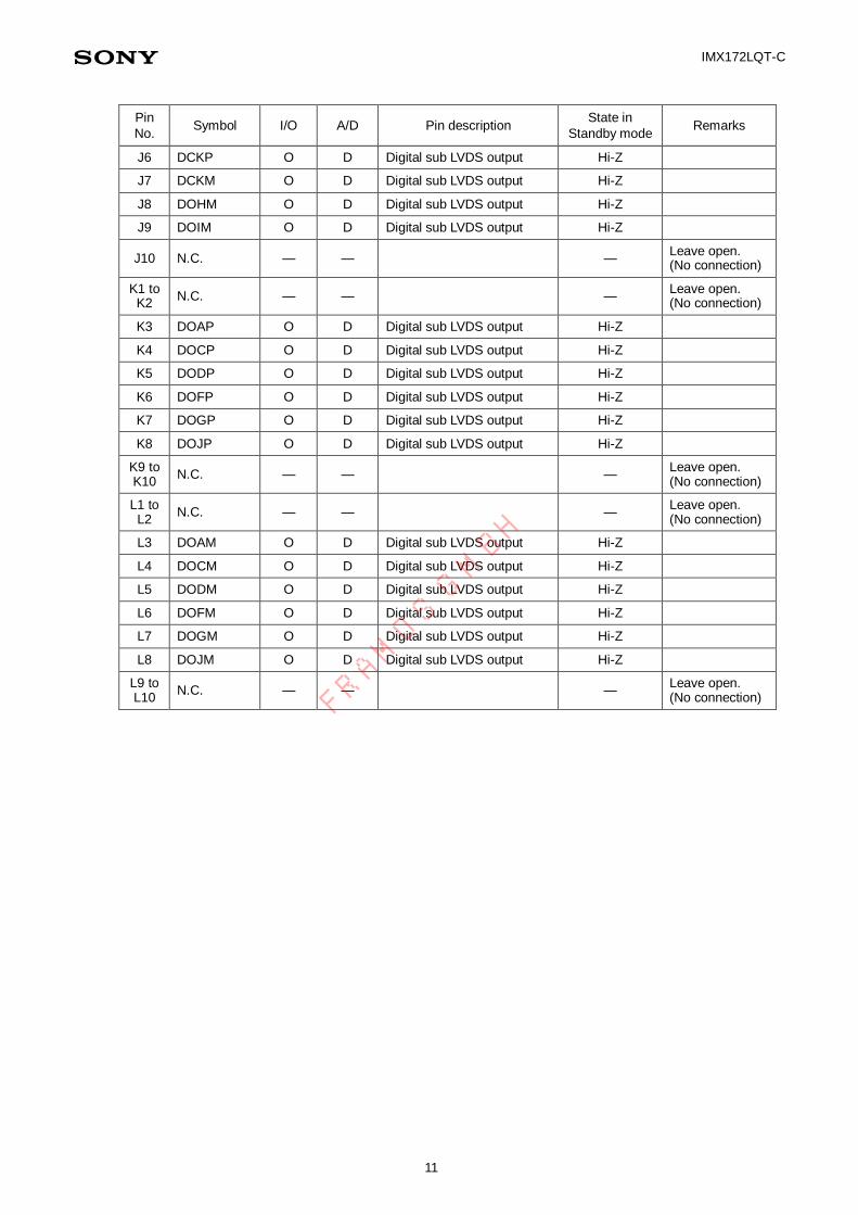
IMX172LQT-C
11
Pin
No. Symbol I/O A/D Pin description
State in
Standby mode Remarks
J6 DCKP O D Digital sub LVDS output Hi-Z
J7 DCKM O D Digital sub LVDS output Hi-Z
J8 DOHM O D Digital sub LVDS output Hi-Z
J9 DOIM O D Digital sub LVDS output Hi-Z
J10 N.C. — — — Leave open. (No connection)
K1 to K2
N.C. — — — Leave open. (No connection)
K3 DOAP O D Digital sub LVDS output Hi-Z
K4 DOCP O D Digital sub LVDS output Hi-Z
K5 DODP O D Digital sub LVDS output Hi-Z
K6 DOFP O D Digital sub LVDS output Hi-Z
K7 DOGP O D Digital sub LVDS output Hi-Z
K8 DOJP O D Digital sub LVDS output Hi-Z
K9 to K10
N.C. — — — Leave open. (No connection)
L1 to L2
N.C. — — — Leave open. (No connection)
L3 DOAM O D Digital sub LVDS output Hi-Z
L4 DOCM O D Digital sub LVDS output Hi-Z
L5 DODM O D Digital sub LVDS output Hi-Z
L6 DOFM O D Digital sub LVDS output Hi-Z
L7 DOGM O D Digital sub LVDS output Hi-Z
L8 DOJM O D Digital sub LVDS output Hi-Z
L9 to L10
N.C. — — — Leave open. (No connection)
FRAM
OS GM
BH
Page 12
IMX172LQT-C
12
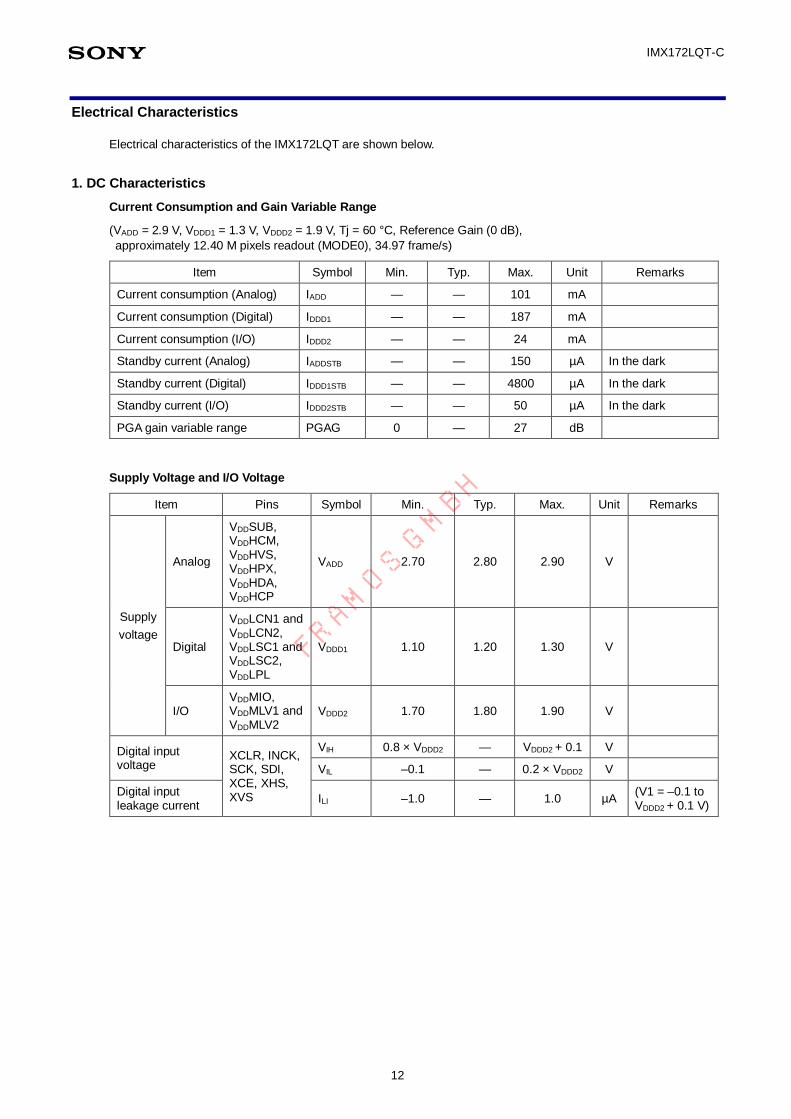
Electrical Characteristics
Electrical characteristics of the IMX172LQT are shown below.
1. DC Characteristics
Current Consumption and Gain Variable Range
(VADD = 2.9 V, VDDD1 = 1.3 V, VDDD2 = 1.9 V, Tj = 60 °C, Reference Gain (0 dB),
approximately 12.40 M pixels readout (MODE0), 34.97 frame/s)
Item Symbol Min. Typ. Max. Unit Remarks
Current consumption (Analog) IADD — — 101 mA
Current consumption (Digital) IDDD1 — — 187 mA
Current consumption (I/O) IDDD2 — — 24 mA
Standby current (Analog) IADDSTB — — 150 µA In the dark
Standby current (Digital) IDDD1STB — — 4800 µA In the dark
Standby current (I/O) IDDD2STB — — 50 µA In the dark
PGA gain variable range PGAG 0 — 27 dB
Supply Voltage and I/O Voltage
Item Pins Symbol Min. Typ. Max. Unit Remarks
Supply
voltage
Analog
VDDSUB, VDDHCM, VDDHVS, VDDHPX, VDDHDA, VDDHCP
VADD 2.70 2.80 2.90 V
Digital
VDDLCN1 and VDDLCN2, VDDLSC1 and VDDLSC2, VDDLPL
VDDD1 1.10 1.20 1.30 V
I/O VDDMIO, VDDMLV1 and VDDMLV2
VDDD2 1.70 1.80 1.90 V
Digital input voltage
XCLR, INCK, SCK, SDI, XCE, XHS, XVS
VIH 0.8 × VDDD2 — VDDD2 + 0.1 V
VIL –0.1 — 0.2 × VDDD2 V
Digital input leakage current
ILI –1.0 — 1.0 µA (V1 = –0.1 to VDDD2 + 0.1 V)
FRAMOS G
MBH
Page 13
IMX172LQT-C
13
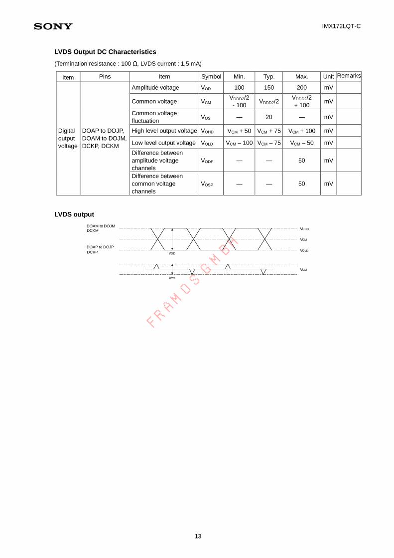
LVDS Output DC Characteristics
(Termination resistance : 100 Ω, LVDS current : 1.5 mA)
Item Pins Item Symbol Min. Typ. Max. Unit Remarks
Digital
output
voltage
DOAP to DOJP,
DOAM to DOJM,
DCKP, DCKM
Amplitude voltage VOD 100 150 200 mV
Common voltage VCM VDDD2/2
- 100 VDDD2/2
VDDD2/2
+ 100 mV
Common voltage
fluctuation VOS — 20 — mV
High level output voltage VOHD VCM + 50 VCM + 75 VCM + 100 mV
Low level output voltage VOLD VCM – 100 VCM – 75 VCM – 50 mV
Difference between
amplitude voltage
channels
VODP — — 50 mV
Difference between
common voltage
channels
VOSP — — 50 mV
LVDS output
VCM
VOHD
VOLDVOD
VCM
VOS
DOAM to DOJMDCKM
DOAP to DOJP
DCKP
FRAMOS G
MBH
Page 14
IMX172LQT-C
14
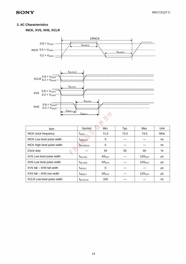
2. AC Characteristics
INCK, XVS, XHS, XCLR
tWLINCK
tWHINCK
1/fINCK
0.8 × VDDD2
INCK
XVS
tWLXVS
XHS
tWLXHS
tHFDLY
tHRDLY
XCLR
tWLXCLR
0.5 × VDDD2
0.2 × VDDD2
0.8 × VDDD2
0.8 × VDDD2
0.8 × VDDD2
0.2 × VDDD2
0.2 × VDDD2
0.2 × VDDD2
Item Symbol Min. Typ. Max. Unit
INCK clock frequency fINCK 71.0 72.0 73.0 MHz
INCK Low level pulse width tWLINCK 5 — — ns
INCK High level pulse width tWHOMCK 5 — — ns
Clock duty — 40 50 60 %
XVS Low level pulse width tWLXVS 4/fINCK — 12/fINCK µs
XHS Low level pulse width tWLXHS 4/fINCK — 12/fINCK µs
XVS fall – XHS fall width tHFDLY 0 — — µs
XVS fall – XHS rise width tHRDLY 4/fINCK — 12/fINCK µs
XCLR Low level pulse width tWLXCLR 100 — — ns
FRAMOS G
MBH
Page 15
IMX172LQT-C
15
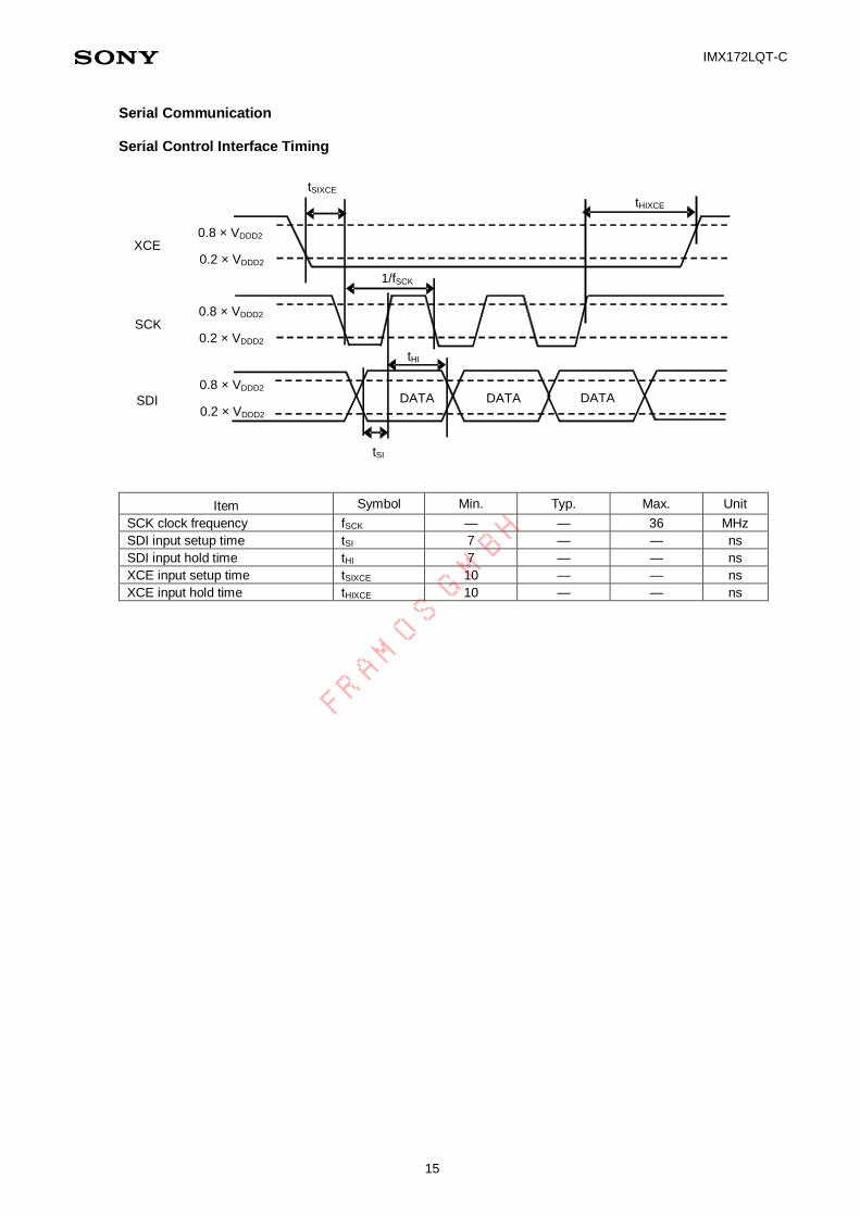
Serial Communication Serial Control Interface Timing
XCE
tSIXCE
SCK
1/fSCK
SDI DATADATADATA
tSI
tHI
tHIXCE
0.8 × VDDD2
0.2 × VDDD2
0.8 × VDDD2
0.2 × VDDD2
0.8 × VDDD2
0.2 × VDDD2
Item Symbol Min. Typ. Max. Unit
SCK clock frequency fSCK — — 36 MHz
SDI input setup time tSI 7 — — ns
SDI input hold time tHI 7 — — ns
XCE input setup time tSIXCE 10 — — ns
XCE input hold time tHIXCE 10 — — ns
FRAMOS G
MBH
Page 16
IMX172LQT-C
16
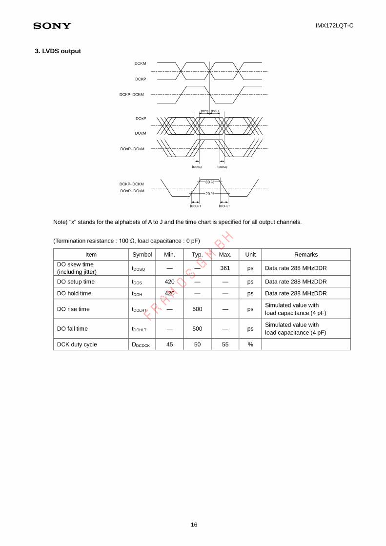
3. LVDS output
DCKP
DCKM
DOxM
DOxP
DOxP – DOxM
DOxP – DOxM
tDOSQtDOSQ
DCKP – DCKM
20 %
80 %
tDOLHT tDOHLT
tDOS tDOH
DCKP – DCKM
Note) "x" stands for the alphabets of A to J and the time chart is specified for all output channels.
(Termination resistance : 100 Ω, load capacitance : 0 pF)
Item Symbol Min. Typ. Max. Unit Remarks
DO skew time
(including jitter) tDOSQ — — 361 ps Data rate 288 MHzDDR
DO setup time tDOS 420 — — ps Data rate 288 MHzDDR
DO hold time tDOH 420 — — ps Data rate 288 MHzDDR
DO rise time tDOLHT — 500 — ps Simulated value with
load capacitance (4 pF)
DO fall time tDOHLT — 500 — ps Simulated value with
load capacitance (4 pF)
DCK duty cycle DDCDCK 45 50 55 %
FRAMOS G
MBH
Page 17
IMX172LQT-C
17
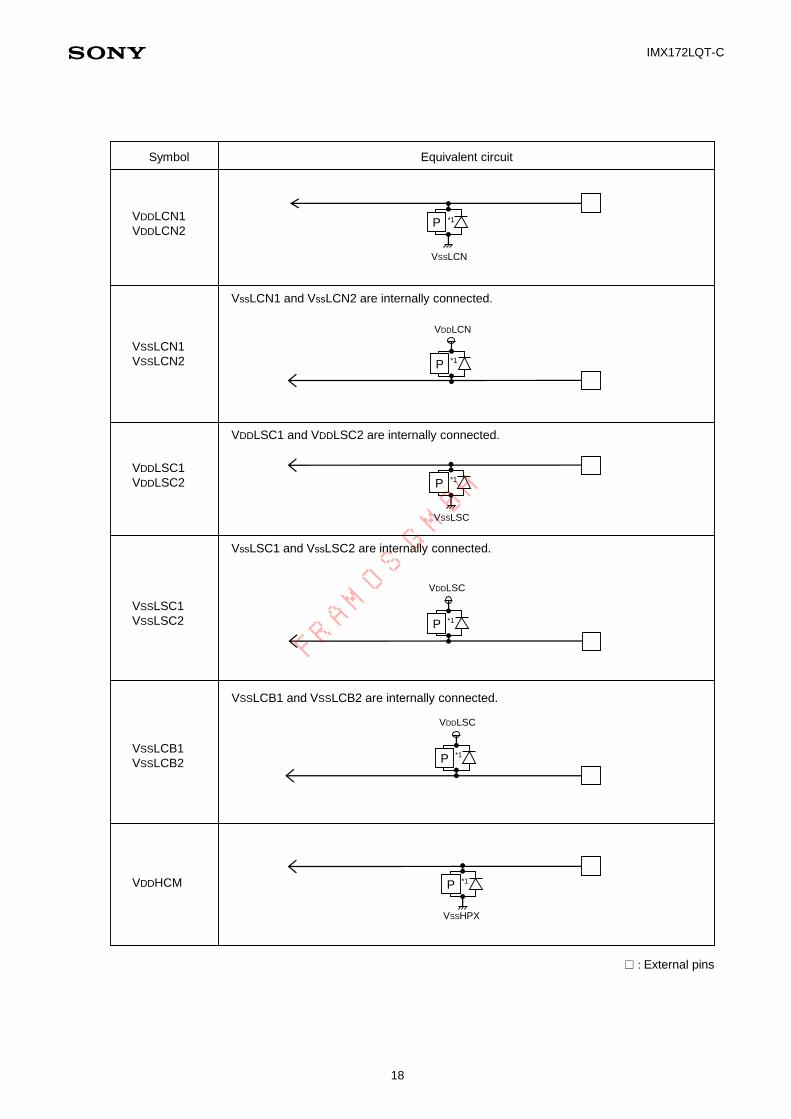
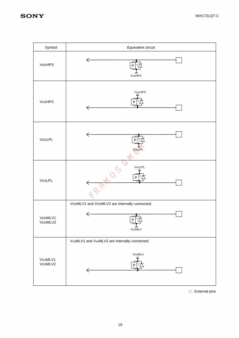
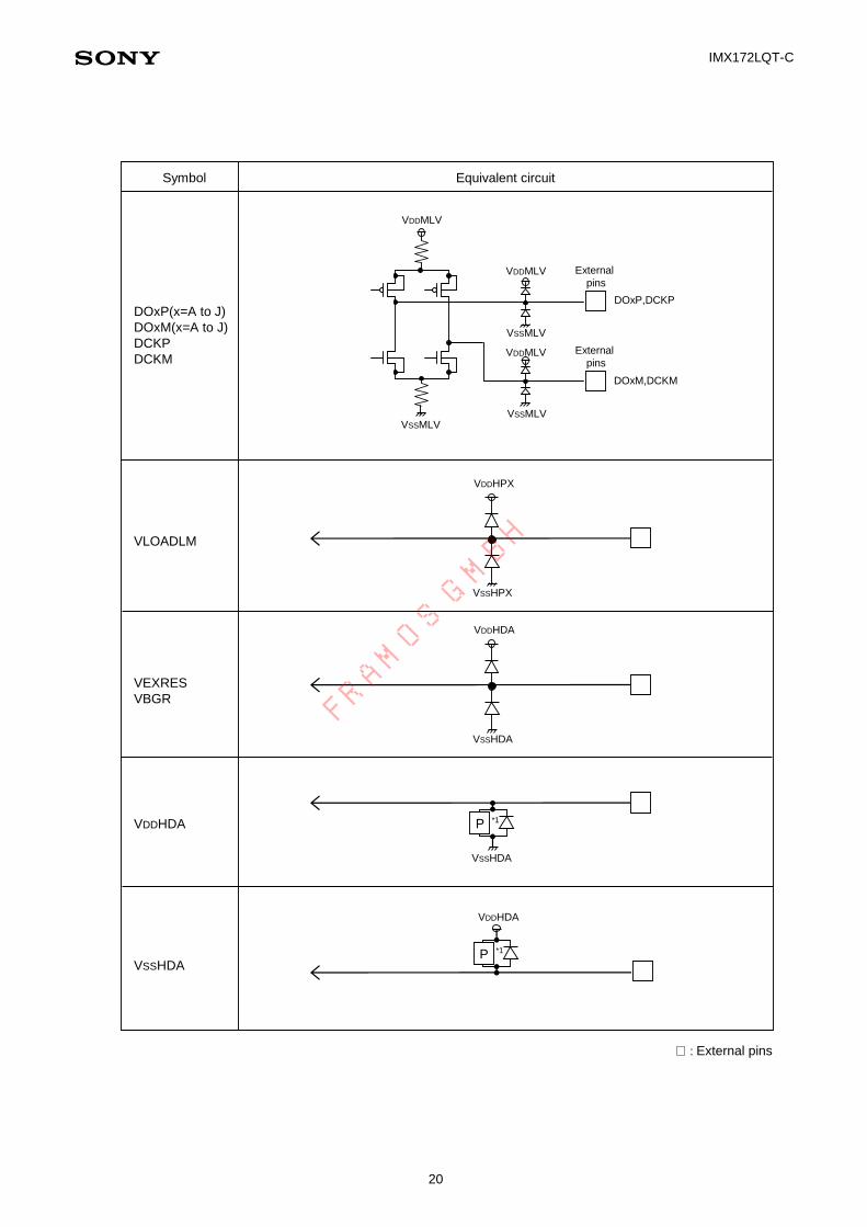
I/O Equivalent Circuit Diagram
Symbol Equivalent circuit
VDDSUBP
VSSLSC
XCLRVSSLSC
P
VDDMIO
VSSLSC
XCE
SCK
SDI
XHS
XVS
INCK
VDDMIO
VSSLSC
VSSLSC
VDDMIO
VDDMIO
VSSLSC
P
SDO
VSSLSC
VDDMIO
VDDMIO
VSSLSC
*1
*1
*1
VDDLSC
VSSLSC
□ : External pins
FRAMOS G
MBH
Page 18
IMX172LQT-C
18
VDDLCN1
VDDLCN2P
VSSLCN
VSSLCN1
VSSLCN2 P
VDDLCN
VDDLSC1
VDDLSC2
VSSLSC1
VSSLSC2
P
VSSLSC
P
VDDLSC
VSSLCB1
VSSLCB2 P
VDDLSC
VDDHCM
VSSHPX
P
*1
*1
*1
*1
*1
*1
VssLSC1 and VssLSC2 are internally connected.
VDDLSC1 and VDDLSC2 are internally connected.
VssLCN1 and VssLCN2 are internally connected.
VSSLCB1 and VSSLCB2 are internally connected.
Symbol Equivalent circuit
□ : External pins
FRAMOS G
MBH
Page 19
IMX172LQT-C
19
VSSHPX P
VDDHPX
VDDLPL
VSSLPL
VSSLPL
P
P
VDDLPL
VDDMLV1
VDDMLV2
VDDMLV1 and VDDMLV2 are internally connected.
VSSMLV1
VSSMLV2 P
VDDMLV
VSSMLV
P
VDDHPX
*1
*1
*1
*1
*1
VssMLV1 and VssMLV2 are internally connected.
VSSHPX
P *1
Symbol Equivalent circuit
□ : External pins
FRAMOS G
MBH
Page 20
IMX172LQT-C
20
VSSHPX
VDDHPX
VLOADLM
VEXRES
VBGR
VSSHDA
VDDHDA
VDDHDA
VSSHDA
VSSHDA
P
P
VDDHDA
DOxP(x=A to J)
DOxM(x=A to J)
DCKP
DCKM
DOxP,DCKP
DOxM,DCKM
VDDMLV
VSSMLVVSSMLV
VDDMLV
VSSMLV
VDDMLV
*1
*1
External
pins
External
pins
Symbol Equivalent circuit
□ : External pins
FRAMOS G
MBH
Page 21
IMX172LQT-C
21
VSSHCP
VDDHCP
VSSHCP
P
P
VDDHCP
VSSHVS
VDDHVS
VRLS
VRLT
VSSHVS
P
P
VDDHVS
P
VSSHVS
(protection circuit with thyristor)
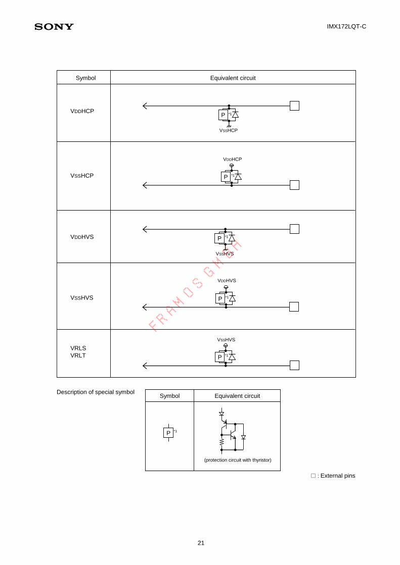
Description of special symbolSymbol Equivalent circuit
P
*1
*1
*1
*1
*1
*1
Symbol Equivalent circuit
□ : External pins
FRAMOS G
MBH
Page 22
IMX172LQT-C
22
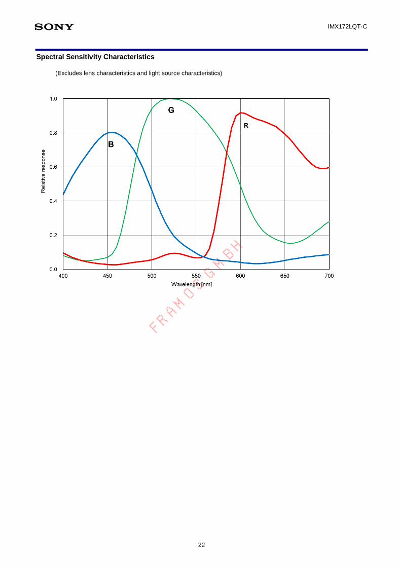
Spectral Sensitivity Characteristics
(Excludes lens characteristics and light source characteristics)
FRAMOS G
MBH
Page 23
IMX172LQT-C
23
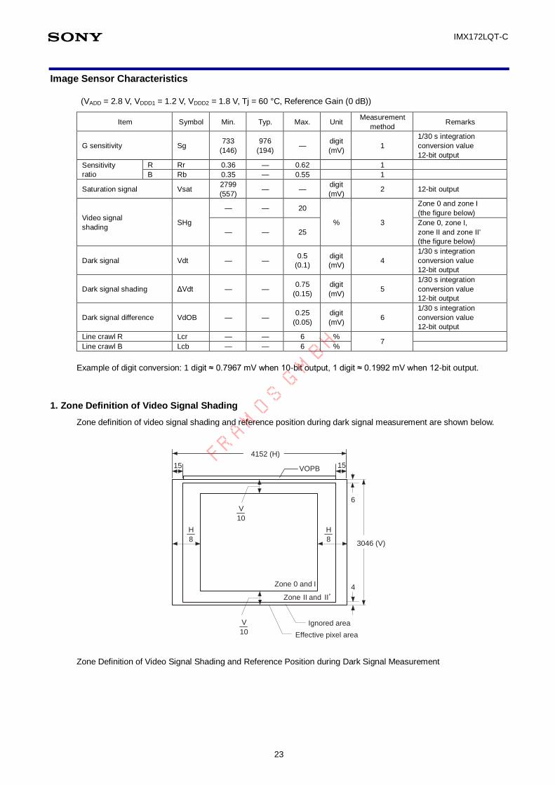
Image Sensor Characteristics
(VADD = 2.8 V, VDDD1 = 1.2 V, VDDD2 = 1.8 V, Tj = 60 °C, Reference Gain (0 dB))
Item Symbol Min. Typ. Max. Unit Measurement
method Remarks
G sensitivity Sg 733
(146)
976
(194) —
digit
(mV) 1
1/30 s integration
conversion value
12-bit output
Sensitivity
ratio
R Rr 0.36 — 0.62 1
B Rb 0.35 — 0.55 1
Saturation signal Vsat 2799
(557) — —
digit
(mV) 2 12-bit output
Video signal
shading SHg
— — 20
% 3
Zone 0 and zone I
(the figure below)
— — 25
Zone 0, zone I,
zone II and zone II'
(the figure below)
Dark signal Vdt — — 0.5
(0.1)
digit
(mV) 4
1/30 s integration
conversion value
12-bit output
Dark signal shading ΔVdt — — 0.75
(0.15)
digit
(mV) 5
1/30 s integration
conversion value
12-bit output
Dark signal difference VdOB — — 0.25
(0.05)
digit
(mV) 6
1/30 s integration
conversion value
12-bit output
Line crawl R Lcr — — 6 % 7
Line crawl B Lcb — — 6 %
Example of digit conversion: 1 digit ≈ 0.7967 mV when 10-bit output, 1 digit ≈ 0.1992 mV when 12-bit output.
1. Zone Definition of Video Signal Shading
Zone definition of video signal shading and reference position during dark signal measurement are shown below.
15 15
4152 (H)
VOPB
6
4
Ignored area
Effective pixel area
Zone 0 and I
Zone II and II’
V
10
3046 (V)
V
10
H
8
H
8
Zone Definition of Video Signal Shading and Reference Position during Dark Signal Measurement
FRAMOS G
MBH
Page 24
IMX172LQT-C
24
Image Sensor Characteristics Measurement Method
1. Measurement Conditions
(1) In the following measurements, the device drive conditions are at the typical values of the bias conditions and
clock voltage conditions.
(2) In the following measurements, spot pixels are excluded and, unless otherwise specified, the optical black
(OB) level is used as the reference for the signal output, which is taken as the value of the Gr/Gb channel
signal output or the R/B channel signal output of the measurement system.
2. Color Coding of this Image Sensor and Readout
The primary color filters of this image sensor are arranged in the layout shown in the figure below. Gr and Gb
represent the G signal on the same line as the R and B signals, respectively. The Gb signal and B signal lines and
the R signal and Gr signal lines are output successively.
Gb B Gb B
R Gr R Gr
Gb B Gb B
R Gr R Gr
Color Coding Diagram
3. Definition of Standard Imaging Conditions
◆ Standard imaging condition I:
Use a pattern box (luminance: 706 cd/m2, color temperature of 3200 K halogen source) as a subject.
(Pattern for evaluation is not applicable.) Use a testing standard lens with CM500S (t = 1.0 mm) as an IR cut filter
and image at F5.6. The luminous intensity to the sensor receiving surface at this point is defined as the standard
sensitivity testing luminous intensity.
◆ Standard imaging condition II:
Image a light source (color temperature of 3200 K) with a uniformity of brightness within 2 % at all angles.
Use a testing standard lens with CM500S (t = 1.0 mm) as an IR cut filter. The luminous intensity is adjusted to the
value indicated in each testing item by the lens diaphragm.
◆ Standard imaging condition III:
Image a light source (color temperature of 3200 K) with a uniformity of brightness within 2 % at all angles.
Use a testing standard lens (exit pupil distance -27.1 mm) with CM500S (t = 1.0 mm) as an IR cut filter.
The luminous intensity is adjusted to the value indicated in each testing item by the lens diaphragm.
1. G sensitivity, Sensitivity ratio
Set the measurement condition to the standard imaging condition I. After setting the electronic shutter mode
witha shutter speed of 1/149.9 s, measure the Gr, Gb, R and B signal outputs (VGr, VGb, VR and VB) at the
center ofthe screen, and substitute the values into the following formula.
VG = (VGr + VGb) /2
Sg = VG × 149.9/30 [mV]
Rr = VR/VG
Rb = VB/VG
2. Saturation signal
Set the measurement condition to the standard imaging condition II. Adjust the luminous intensity to 20 times the
intensity with the average value of the G ( = (Gr + Gb) / 2) signal output, 194 [mV] .
Measure the minimum values of the Gr, Gb, R and B signals when shooting in rolling shutter mode.
FRAMOS G
MBH
Page 25
IMX172LQT-C
25
3. Video signal shading
Set the measurement condition to the standard imaging condition II. With the lens diaphragm at F5.6 to F8,
adjust the luminous intensity so that the average value of the G signal output is 194 [mV] .
Then measure the maximum value (Gmax [mV]) and the minimum value (Gmin [mV]) of the G signal output,
and substitute the values into the following formula.
SHg = (Gmax – Gmin) / 194 × 100 [%]
4. Dark signal
Measure the average value (Vdt [mV]) of the signal output in zone 0 to zone II’ in the light-obstructed state.
Define the average value of the signal output accumulated in 1 frame period (t1v) as Vdt1V and the average
value of the signal output accumulated in the shortest period (1H period: t1h) as Vdt1H, and then substitute the
values into the following formula.
Vdt = (Vdt1V – Vdt1H) / (t1v – t1h) / 30 [mV]
5. Dark signal shading
Following the item 4, measure the maximum value (Vdmax [mV]) and minimum value (Vdmin [mV]) of the dark
signal output, and substitute the values into the following formula.
ΔVdt = Vdmax – Vdmin [mV]
6. Dark signal difference
Following the item 5, measure the average value of the dark signal output (VdOB [mV]) in zone 0 to zone II'
using the optical black (vertical direction VOPB area) level as a reference.
7. Line crawl
Set the measurement condition to the standard imaging condition II. After adjusting the average value of the
G ( = (Gr + Gb) / 2) signal output when inserting G filter to 194 [mV] , measure the average values of the Gr
and Gb signal output (GGr, GGb).
After adjusting the average value of the R signal output when inserting R filter to 194 [mV] , measure the
average values of the Gr and Gb signal output (RGr, RGb).
Substitute the values into the following formula.
Lcr = {RGr – (GGr / GGb) × RGb} / [{RGr + (GGr / GGb) × RGb} / 2] × 100 [%]
Then, after adjusting the average value of the B signal output when inserting B filter to 194 [mV] , measure
the average values of the Gr and Gb signal output (BGr, BGb). Substitute the values into the following
formula.
Lcb = {BGb – (GGb / GGr) × BGr} / [{BGb + (GGb / GGr) × BGr} / 2] × 100 [%]
FRAMOS G
MBH
Page 26
IMX172LQT-C
26
Setting Registers by Serial Communication
Sensor operation is controlled by the register settings. Follow the procedure below and make the register settings by
serial communication.
1. Set XCE Low to enable the chip's serial communication function.
2. Transmit serial data (SDI) synchronized with SCK 1 bit at a time from the lower bits.
3. Transmit the Chip ID (fixed value : 81h) in the first byte.
4. Transmit the address value of the register to be set in the second and third bytes.
5. Transmit the register setting value to the address designated by the second and third bytes in the fourth byte.
6. Transmit the register setting value to the address following the address designated by the second and third bytes
in the fifth byte.
7. Transmit the register setting values to subsequent addresses in order thereafter.
8. Set XCE High to end serial communication.
The IMX172LQT clears the Chip ID and address setting data by setting XCE High.
Therefore, the Chip ID and address settings must also be made when the next serial communication is performed.
Continuous write across upper bytes is prohibited. When writing across upper bytes, first complete the above
sequence, and then perform communication again. In addition, when jumping to a discontinuous address, also first
complete the above sequence, and then perform communication again.
Perform serial communication within the 6XHS period (recommended serial communication period) after the fall of
XVS to avoid affecting the image quality.
Settings made by serial communication are basically updated immediately each time 1 byte of setting values is
transmitted. However, in some exceptional cases (electronic shutter setting, etc.), register setting values are updated
immediately before the start of readout immediately after the recommended serial communication period (7th XHS).
For details, see “Register Map” on pages 27 to 30 and “1. Register Value Reflection Timing to Output Data” on page
31.
Note) 1. Communication is always accepted.
2. Communication should be completed within the recommended serial communication period to prevent
noise. However, this restriction does not apply during the readout period of non-picture frames in which
noise is ignored (immediately after power-on or immediately after switching the drive mode, etc.), so
register communication can be performed other than during the communication period of those frames.
3. Communications with the following registers should always be performed within the same recommended
serial communication period. Do not communicate with the 3 registers other than during communication
period, even in non-picture frames in which noise is ignored.
◆ PGC register (address 0009h, bit [7:0] and address 000Ah, bit [2:0])
◆ APGC01 register (address 0352h, bit [7:0] and address 0353h, bit [0])
◆ APGC02 register (address 0356h, bit [7:0] and address 0357h, bit [0])
Example of Serial Communication Timing 1
LSB
Chip ID Start address(Upper 1 byte)
Start address(Lower 1 byte)
N byte data
6 7
LSB LSB MSBLSB
0 2 54 737
XCE
SCK
Data established
timing
SDI16510 243 6510 2743 6510 2
MSB MSB MSB
Example of Serial Communication 1
Example of Serial Communication Timing 2
XCE
SCK
7
M byte data
0 1
LSB
Chip ID Start address(Upper 1 byte)
Start address(Lower 1 byte)
N byte data
1
LSB MSB
0 7
MSB
6 76610
MSB
Data established
timing
SDILSBMSB
6 76
Chip ID
LSB MSB
Start address(Upper 1 byte)
Start address(Lower 1 byte)
7 061007610 1107
LSB
1
LSB MSBLSB
6 7
LSBMSBMSB
Example of Serial Communication 2
FRAMOS G
MBH
Page 27
IMX172LQT-C
27
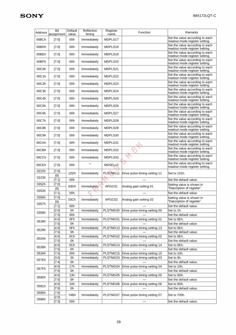
Register Map
The register map is given below.
Address Bit
assignment Default value
Reflection timing
Register name
Function Remarks
0000h
[0] 1h Immediately STANDBY 0h : Normal operation 1h : Overall standby
Setting range: 0h to 1h
[1] 1h Immediately STBLOGIC
0h: Normal operation
1h: Digital circuit standby other than serial communications block
Setting range: 0h to 1h
[7:2] 01h — Set the default value.
0001h
[0] 0h Immediately DCKRST When changed from 0h to 1h:
Fixes the LVDS clock output phase
Setting range: 0h to 1h After fixing the LVDS clock output phase, the value is automatically returned to 0h.
[3:1] 0h — Set the default value.
[4] 0h Communication
end frame *1
CLPSQRST
When changed from 0h to 1h:
Resets the internal clamp circuit
operation mode
Setting range: 0h to 1h After the reset, the value is automatically returned to 0h.
[7:5] 0h — Set the default value.
0002h [0] 0h
*1 SSBRK
When changed from 0h to 1h:
Interrupt enable
Setting range: 0h to 1h After the interrupt, the value is automatically returned to 0h.
[7:1] 00h — Set the default value.
0003h
[3:0] 0h *1
STBLVDS
0h : 10 ch 1h : 8 ch 3h : 4 ch Fh : All channel standby
Allowable setting values are 0h, 1h, 3h, and Fh.
[6:4] 4h *1
CHSEL
Number of LVDS output channels selection 0h : 10 ch 1h : 8 ch 3h : 4 ch
Allowable setting values are 0h, 1h, and 3h
[7] 0h — Set the default value.
0004h [7:0] 2Ah *1
MDSEL1 Set the value according to each readout mode register setting.
0005h [7:0] 1Ch *1
MDSEL2 Set the value according to each readout mode register setting.
0006h [7:0] 00h *1
MDSEL3 Set the value according to each readout mode register setting.
0007h [7:0] 00h *1
MDSEL4 Set the value according to each readout mode register setting.
0008h [7:0] 00h — Set the default value.
0009h [7:0] 000h Immediately PGC Analog gain setting
Setting range: 0h to 7A5h
000Ah [2:0]
[7:3] 00h — Set the default value.
000Bh [7:0]
0007h
Next frame
after communication
end *2
SHR Specifies the integration start
horizontal period Setting range is shown in ”Description of Registers” 000Ch [7:0]
000Dh [7:0] 0000h
*2 SVR
Specifies the integration shutdown vertical period
Setting range: 0h to FFFFh 000Eh [7:0]
000Fh [7:0] 0000h
*2 SPL
Specifies the integration start
vertical period Setting range: 0h to FFFFh 0010h [7:0]
FRAMOS G
MBH
Page 28
IMX172LQT-C
28
Address Bit
assignment Default value
Reflection timing
Register name
Function Remarks
0011h [1:0]
0h
*1 DGAIN
Digital gain setting
0h : 0 dB gain setting value
1h : +6 dB gain setting value
2h : +12 dB gain setting value
3h : +18 dB gain setting value
Setting range: 0h to 3h
[7:2] 00h — Set the default value.
0012h [0] 0h
*1 FREQ
0h: (INCK × 4) MHz-DDR output
1h: (INCK × 2) MHz-DDR output
Setting range: 0h to 1h
[7:1] 00h — Set the default value.
001Ah [0] 0h
*1 MDVREV
0h : Vertical direction normal readout
1h : Vertical direction inversion readout
Setting range: 0h to 1h
[7:1] 00h — Set the default value.
0026h [7:0] 74h *1
MDSEL13 Set the value according to each readout mode register setting.
0027h [7:0] 74h *1
MDSEL14 Set the value according to each readout mode register setting.
0028h [7:0] 74h *1
MDSEL15 Set the value according to each readout mode register setting.
0045h [7:0] 32h Immediately BLKLEVEL Digital black level offset setting
Setting range: 0h to FFh 10-bit readout mode : 1 digit/1h 12-bit readout mode : 4 digit/1h
007Eh [7:0] 0000h
*1 MDSEL5
Set the value according to each readout mode register setting. 007Fh [7:0]
0080h [7:0] 00h Immediately MDPLS01 Set the value according to each readout mode register setting.
0081h [7:0] 00h Immediately MDPLS02 Set the value according to each readout mode register setting.
0082h [7:0] 00h Immediately MDPLS03 Set the value according to each readout mode register setting.
0083h [7:0] 00h Immediately MDPLS04 Set the value according to each readout mode register setting.
0084h [7:0] 00h Immediately MDPLS05 Set the value according to each readout mode register setting.
0085h [7:0] 00h Immediately MDPLS06 Set the value according to each readout mode register setting.
0086h [7:0] 00h Immediately MDPLS07 Set the value according to each readout mode register setting.
0087h [7:0] 00h Immediately MDPLS08 Set the value according to each readout mode register setting.
0095h [7:0] 00h Immediately MDPLS09 Set the value according to each readout mode register setting.
0096h [7:0] 00h Immediately MDPLS10 Set the value according to each readout mode register setting.
0097h [7:0] 00h Immediately MDPLS11 Set the value according to each readout mode register setting.
0098h [7:0] 00h Immediately MDPLS12 Set the value according to each readout mode register setting.
0099h [7:0] 00h Immediately MDPLS13 Set the value according to each readout mode register setting.
009Ah [7:0] 00h Immediately MDPLS14 Set the value according to each readout mode register setting.
009Bh [7:0] 00h Immediately MDPLS15 Set the value according to each readout mode register setting.
009Ch [7:0] 00h Immediately MDPLS16 Set the value according to each readout mode register setting.
00B6h [7:0] 00h Immediately MDSEL6 Set the value according to each readout mode register setting.
00B7h [7:0] 00h Immediately MDSEL7 Set the value according to each readout mode register setting.
00B8h [7:0] 00h Immediately MDSEL8 Set the value according to each readout mode register setting.
00B9h [7:0] 00h Immediately MDSEL9 Set the value according to each readout mode register setting.
00BAh [7:0] 00h Immediately MDSEL10 Set the value according to each readout mode register setting.
00BBh [7:0] 00h Immediately MDSEL11 Set the value according to each readout mode register setting.
FRAMOS G
MBH
Page 29
IMX172LQT-C
29
Address Bit
assignment Default value
Reflection timing
Register name
Function Remarks
00BCh [7:0] 00h Immediately MDPLS17 Set the value according to each readout mode register setting.
00BDh [7:0] 00h Immediately MDPLS18 Set the value according to each readout mode register setting.
00BEh [7:0] 00h Immediately MDPLS19 Set the value according to each readout mode register setting.
00BFh [7:0] 00h Immediately MDPLS20 Set the value according to each readout mode register setting.
00C0h [7:0] 00h Immediately MDPLS21 Set the value according to each readout mode register setting.
00C1h [7:0] 00h Immediately MDPLS22 Set the value according to each readout mode register setting.
00C2h [7:0] 00h Immediately MDPLS23 Set the value according to each readout mode register setting.
00C3h [7:0] 00h Immediately MDPLS24 Set the value according to each readout mode register setting.
00C4h [7:0] 00h Immediately MDPLS25 Set the value according to each readout mode register setting.
00C5h [7:0] 00h Immediately MDPLS26 Set the value according to each readout mode register setting.
00C6h [7:0] 00h Immediately MDPLS27 Set the value according to each readout mode register setting.
00C7h [7:0] 00h Immediately MDPLS28 Set the value according to each readout mode register setting.
00C8h [7:0] 00h Immediately MDPLS29 Set the value according to each readout mode register setting.
00C9h [7:0] 00h Immediately MDPLS30 Set the value according to each readout mode register setting.
00CAh [7:0] 00h Immediately MDPLS31 Set the value according to each readout mode register setting.
00CBh [7:0] 00h Immediately MDPLS32 Set the value according to each readout mode register setting.
00CCh [7:0] 00h Immediately MDPLS33 Set the value according to each readout mode register setting.
00CEh [7:0] 00h *1
MDSEL12 Set the value according to each readout mode register setting.
0222h [7:0] 12Dh Immediately PLSTMG11 Drive pulse timing setting 11 Set to 131h.
0223h [0]
[7:1] 00h — Set the default value.
0352h [7:0] 03Dh Immediately APGC01 Analog gain setting 01
Setting value is shown in “Description of register”.
0353h [0]
[7:1] 00h — Set the default value.
0356h [7:0] 03Ch Immediately APGC02 Analog gain setting 02
Setting value is shown in “Description of register”.
0357h [0]
[7:1] 00h — Set the default value.
0358h [2:0] 0h Immediately PLSTMG00 Drive pulse timing setting 00 Set to 1h.
[7:3] 00h — Set the default value.
0528h [4:0] 0Fh Immediately PLSTMG01 Drive pulse timing setting 01 Set to 0Eh.
[7:5] 0h — Set the default value.
0529h [4:0] 0Fh Immediately PLSTMG13 Drive pulse timing setting 13 Set to 0Eh.
[7:5] 0h — Set the default value.
052Ah [4:0] 0Ch Immediately PLSTMG02 Drive pulse timing setting 02 Set to 0Eh.
[7:5] 0h — Set the default value.
052Bh [4:0] 0Ch Immediately PLSTMG14 Drive pulse timing setting 14 Set to 0Eh.
[7:5] 0h — Set the default value.
0534h [7:0] 00h Immediately PLSTMG15 Drive pulse timing setting 15 Set to 10h.
057Eh [3:0] 3h Immediately PLSTMG03 Drive pulse timing setting 03 Set to 0h.
[7:4] 0h — Set the default value.
057Fh [4:0] 17h Immediately PLSTMG04 Drive pulse timing setting 04 Set to 10h.
[7:5] 0h — Set the default value.
0580h [4:0] 13h Immediately PLSTMG05 Drive pulse timing setting 05 Set to 0Dh.
[7:5] 0h — Set the default value.
0581h [4:0] 10h Immediately PLSTMG06 Drive pulse timing setting 06 Set to 0Dh.
[7:5] 0h — Set the default value.
0585h [7:0] 74Bh Immediately PLSTMG07 Drive pulse timing setting 07 Set to 700h.
0586h [2:0]
[7:3] 00h — Set the default value.
FRAMOS G
MBH
Page 30
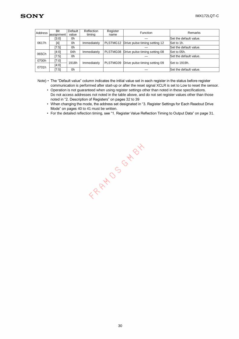
IMX172LQT-C
30
Address Bit
assignment Default value
Reflection timing
Register name
Function Remarks
0617h
[3:0] 0h — Set the default value.
[4] 0h Immediately PLSTMG12 Drive pulse timing setting 12 Set to 1h.
[7:5] 0h — Set the default value.
065Ch [4:0] 04h Immediately PLSTMG08 Drive pulse timing setting 08 Set to 05h.
[7:5] 0h — Set the default value.
0700h [7:0] 1918h Immediately PLSTMG09 Drive pulse timing setting 09 Set to 1919h.
0701h [4:0]
[7:5] 0h — Set the default value.
Note) • The “Default value” column indicates the initial value set in each register in the status before register
communication is performed after start-up or after the reset signal XCLR is set to Low to reset the sensor.
• Operation is not guaranteed when using register settings other than noted in these specifications.
Do not access addresses not noted in the table above, and do not set register values other than those
noted in “2. Description of Registers” on pages 32 to 39
• When changing the mode, the address set designated in “3. Register Settings for Each Readout Drive
Mode” on pages 40 to 41 must be written.
• For the detailed reflection timing, see “1. Register Value Reflection Timing to Output Data” on page 31.
FRAMOS G
MBH
Page 31
IMX172LQT-C
31
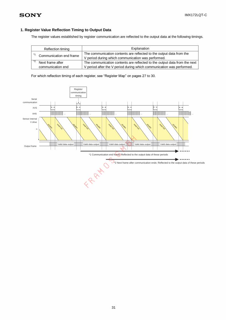
1. Register Value Reflection Timing to Output Data
The register values established by register communication are reflected to the output data at the following timings.
Reflection timing Explanation
*1. Communication end frame
The communication contents are reflected to the output data from the
V period during which communication was performed. *2.
Next frame after
communication end
The communication contents are reflected to the output data from the next
V period after the V period during which communication was performed.
For which reflection timing of each register, see “Register Map” on pages 27 to 30.
XVS
.........XHS
Y
... ......
Serial
communication
Sensor internal
V drive
Output frame
*2 Next frame after communication ends: Reflected to the output data of these periods
*1 Communication end frame: Reflected to the output data of these periods
Register
communication
timing
shutter
read out
Valid data output
6XHS
shutter
read out
shutter
read out
shutter
read out
shutter
read out
shutter
Valid data output Valid data output Valid data output Valid data output
6XHS6XHS6XHS6XHS6XHS
FRAMOS G
MBH
Page 32
IMX172LQT-C
32
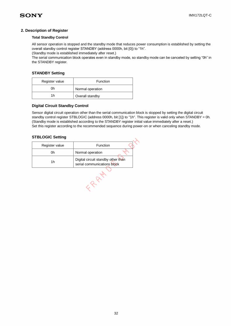
2. Description of Register
Total Standby Control
All sensor operation is stopped and the standby mode that reduces power consumption is established by setting the
overall standby control register STANDBY (address 0000h, bit [0]) to “1h”.
(Standby mode is established immediately after reset.)
The serial communication block operates even in standby mode, so standby mode can be canceled by setting “0h” in
the STANDBY register.
STANDBY Setting
Register value Function
0h Normal operation
1h Overall standby
Digital Circuit Standby Control
Sensor digital circuit operation other than the serial communication block is stopped by setting the digital circuit
standby control register STBLOGIC (address 0000h, bit [1]) to "1h". This register is valid only when STANDBY = 0h.
(Standby mode is established according to the STANDBY register initial value immediately after a reset.)
Set this register according to the recommended sequence during power-on or when canceling standby mode.
STBLOGIC Setting
Register value Function
0h Normal operation
1h Digital circuit standby other than
serial communications block
FRAMOS G
MBH
Page 33
IMX172LQT-C
33
LVDS Clock Output Phase Fixed
The clock phase relative to the sync code start data in the LVDS data output is fixed by the LVDS clock output phase
fixing register DCKRST (address 0001h, bit [0]). Make this setting according to the recommended sequence during
power-on or when canceling standby mode.
This register automatically returns to “0h” after the phase fixing process, so there is no need to write “0h”.
DCKRST Operation Setting
Register value Function
Changed from 0h to 1h Fixes the LVDS clock output phase
Clamp Reset
The internal clamp circuit operation status is reset by the clamp reset register CLPSQRST (address 0001h, bit [4]).
Make this setting according to the recommended sequence during power-on or when canceling standby mode.
This register automatically returns to “0h” after the reset process, so there is no need to write “0h”.
CLPSQRST Operation Setting
Register value Function
Changed from 0h to 1h Resets the internal clamp circuit operation status
Break Mode
XVS can be subsampled according to SVR. This XVS subsampling operation can be stopped and then restarted
from the start of the exposure period using the break mode register SSBRK (address 0002h, bit [0]).This register
automatically returns to “0h” after the break process, so there is no need to write “0h”.
SSBRK Setting
Register value Function
Changed from 0h to 1h Interrupt enable
FRAMOS G
MBH
Page 34
IMX172LQT-C
34
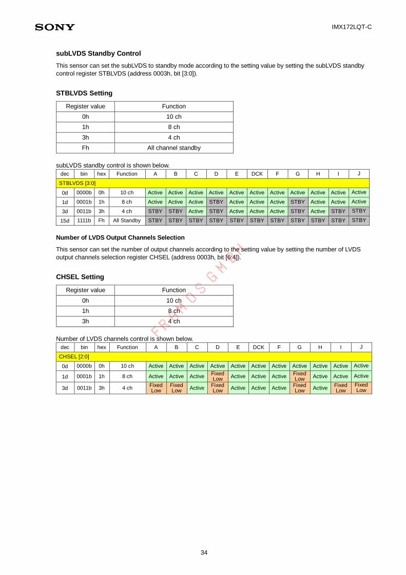
subLVDS Standby Control
This sensor can set the subLVDS to standby mode according to the setting value by setting the subLVDS standby
control register STBLVDS (address 0003h, bit [3:0]).
STBLVDS Setting
Register value Function
0h 10 ch
1h 8 ch
3h 4 ch
Fh All channel standby
subLVDS standby control is shown below.
dec bin hex Function A B C D E DCK F G H I J
STBLVDS [3:0]
0d 0000b 0h 10 ch Active Active Active Active Active Active Active Active Active Active Active
1d 0001b 1h 8 ch Active Active Active STBY Active Active Active STBY Active Active Active
3d 0011b 3h 4 ch STBY STBY Active STBY Active Active Active STBY Active STBY STBY
15d 1111b Fh All Standby STBY STBY STBY STBY STBY STBY STBY STBY STBY STBY STBY
Number of LVDS Output Channels Selection
This sensor can set the number of output channels according to the setting value by setting the number of LVDS
output channels selection register CHSEL (address 0003h, bit [6:4]).
CHSEL Setting
Register value Function
0h 10 ch
1h 8 ch
3h 4 ch
Number of LVDS channels control is shown below.
dec bin hex Function A B C D E DCK F G H I J
CHSEL [2:0]
0d 0000b 0h 10 ch Active Active Active Active Active Active Active Active Active Active Active
1d 0001b 1h 8 ch Active Active Active Fixed Low
Active Active Active Fixed Low
Active Active Active
3d 0011b 3h 4 ch Fixed Low
Fixed Low
Active Fixed Low
Active Active Active Fixed Low
Active Fixed Low
Fixed Low
FRAMOS G
MBH
Page 35
IMX172LQT-C
35
Electronic Shutter Timing
The exposure start timing can be designated by setting the electronic shutter timing register SHR (address 000Bh, bit
[7:0] and address 000Ch, bit [7:0]). Designate the lower 8 bits in address 000Bh and the upper 8 bits in address
000Ch, for a total of 16 bits.
Note that this setting value unit is 1XHS period regardless of the readout drive mode. In addition, the vertical sync
signal XVS can be subsampled inside the sensor according to the SVR register (address 000Dh, bit [7:0] and
address 000Eh, bit [7:0]). The vertical sync signal period is treated as SVR + 1 inside the sensor.
When setting the electronic shutter during the vertical sync signal subsampling period, the SPL register (address
000Fh, bit [7:0] and address 0010h, bit [7:0]) is available.
Shutter Setting
Register Register value Function
SHR
8 to {(SVR + 1) × Number of XHS pulses per frame – 4}
Readout mode No.0, 1, 2, 3, 4 All-pixel scan mode (12 bits/10 bits)
Specifies the integration start horizontal period
10 to {(SVR + 1) × Number of XHS pulses per frame – 4}
Readout mode No.5,
Horizontal/vertical 2/2-line binning mode
SVR 0h to FFFFh *Note 2.
Specifies the integration shutdown vertical period
SPL 0h to FFFFh *Note 2.
Specifies the integration start vertical period
Note) 1. See “Integration Time in Each Readout Drive Mode” on page 55 for the integration time calculation
formula.
2. The SVR and SPL register definition areas are guaranteed as sensor functions, but the characteristics are
not guaranteed.
FRAMOS G
MBH
Page 36
IMX172LQT-C
36
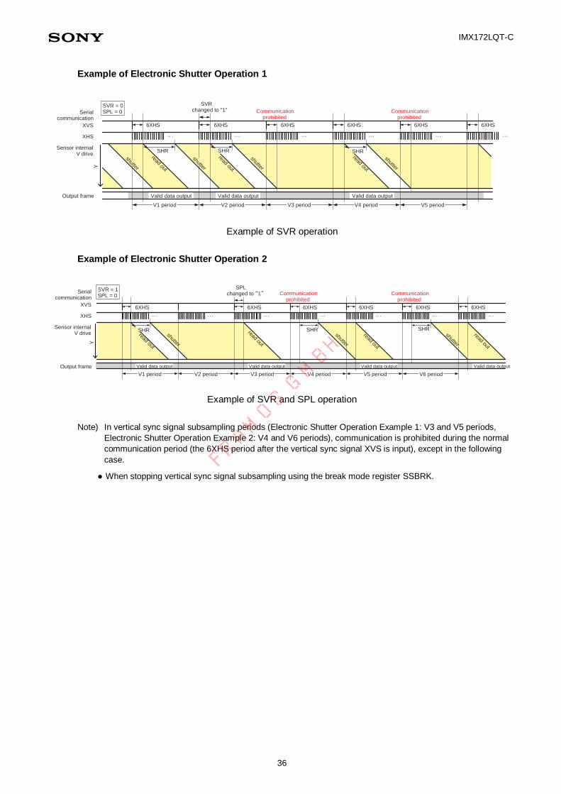
Example of Electronic Shutter Operation 1
XVS
XHS
Serial communication
Sensor internal V drive
.........
Y
SHR
......
Valid data outputValid data outputValid data output
V4 periodV2 periodV1 period
SHR
.. .
SHR
SHX6SHX6SHX6SHX6SHX6SHX6
SVR = 0SPL = 0
SVRchanged to "1" Communication
prohibitedCommunication
prohibited
V5 periodV3 period
Output frame
shutter
read out
shutter
read out
shutter
read out
shutter
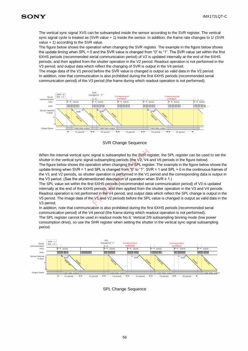
Example of SVR operation
Example of Electronic Shutter Operation 2
Valid data output Valid data output Valid data output
V1 period V3 period V5 period
6XHS6XHS6XHS6XHS6XHS6XHS
Valid data output
...... .. . .. ... .
SHR SHR
SPLchanged to “1”
.. .
SVR = 1SPL = 0
SHR
.. .
Communicationprohibited
Communicationprohibited
V2 period V4 period V6 period
shutter
read out
read out
XVS
XHS
Serial communication
Sensor internal V drive
Y
Output frame
shutter
read out
shutter
read out
Example of SVR and SPL operation
Note) In vertical sync signal subsampling periods (Electronic Shutter Operation Example 1: V3 and V5 periods,
Electronic Shutter Operation Example 2: V4 and V6 periods), communication is prohibited during the normal
communication period (the 6XHS period after the vertical sync signal XVS is input), except in the following
case.
When stopping vertical sync signal subsampling using the break mode register SSBRK.
FRAMOS G
MBH
Page 37
IMX172LQT-C
37
Analog Gain
The analog gain value can be set by setting the analog gain register PGC (address 0009h, bit [7:0] and address
000Ah, bit [2:0]). Set the lower 8 bits in address 0009h and the upper 3 bits in address 000Ah, for a total of 11 bits.
In addition, change APGC01 (address 0352h, bit [7:0] and address 0353h, bit [0]) and APGC02 (address 0356h, bit
[7:0] and address 0357h, bit [0]) linked with the analog gain register PGC. Communications with PGC, APGC01 and
APGC02 should always be performed within the same recommended serial communication period. Do not
communicate with the 3 registers other than during communication period, even in non-picture frames in which noise
is ignored.
The values to be written are different with PGC setting and readout drive mode. See the following "APGC01 and
APGC02 setting"for the detailed specifications.
PGC Setting
Register value Function
0h to 7A5h (0d to 1957d)
Analog gain setting
APGC01 and APGC02 Setting
PGC setting
Modes other than readout drive mode No.0,2,3
*1
Readout drive mode No.0,2,3 *1
APGC01 setting APGC02 setting APGC01 setting APGC02 setting
0h to 146h 01Fh 01Eh
03Dh 03Ch
147h to 400h 021h 020h
401h to 52Ch 026h 025h
52Dh to 696h 028h 027h
697h to 74Bh 02Ch 02Bh
74Ch to 7A5h 030h 02Fh
*1. See “1. Readout Drive Modes” on pages 42 for details of readout mode No.
In addition, the figure below shows the relationship between the register setting value and the set gain value.
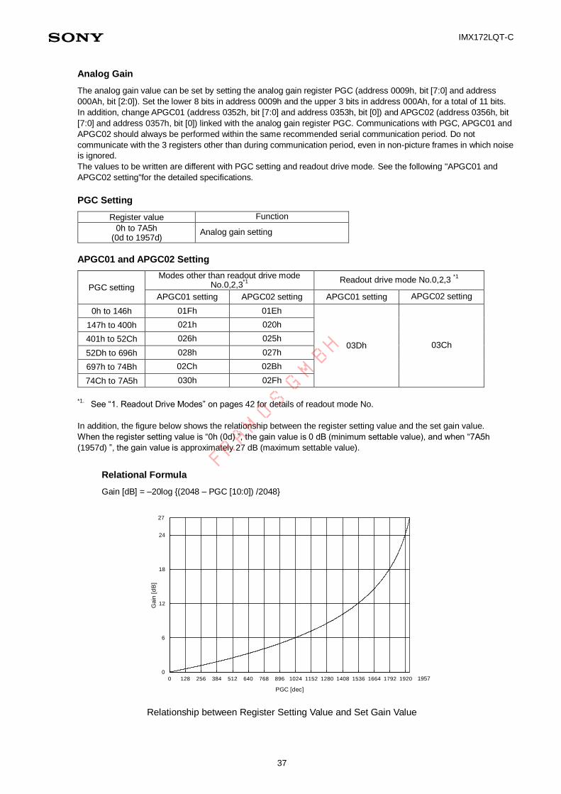
When the register setting value is “0h (0d) ”, the gain value is 0 dB (minimum settable value), and when “7A5h
(1957d) ”, the gain value is approximately 27 dB (maximum settable value).
Relational Formula
Gain [dB] = –20log {(2048 – PGC [10:0]) /2048}
Relationship between Register Setting Value and Set Gain Value
0
6
12
18
24
0 128 256 384 512 640 768 896 1024 1152 1280 1408 1536 1664 1792 1920
Gain
[d
B]
PGC [dec]
27
1957
FRAMOS G
MBH
Page 38
IMX172LQT-C
38
Digital Gain
The digital gain applied to the data after pixel binning can be set by the digital gain setting register DGAIN (address
0011h, bit [1:0]).
DGAIN Setting
Register value Function
0h Digital gain setting value = 0 dB
1h Digital gain setting value = +6 dB
2h Digital gain setting value = +12 dB
3h Digital gain setting value = +18 dB
Output Format
The LVDS-I/F output frequency can be set by the output format setting register, FREQ (address 0012h, bit [0]).
The readout drive mode in this data sheet is specified under the condition of FREQ = 0h. The data rate and the frame
frequency are the half of the described values when set to FREQ = 1h.
FREQ Setting
Register value Function
0h (INCK × 4) MHz-DDR output
1h (INCK × 2) MHz-DDR output
Vertical Direction Readout Inversion
The direction of vertical readout order can be set by the vertical direction readout inversion register MDVREV
(address 001Ah, bit [0]).
MDVREV Setting
Register value Function
0h Vertical direction normal readout
1h Vertical direction inversion readout
Digital Black Level Offset
The black level offset applied to the data after digital gain processing by the DGAIN register is set by the digital black
level offset setting register BLKLEVEL (address 0045h, bit [7:0]).
Note that the offset unit changes according to the readout drive mode.
When the output data length is 10-bit output, increasing the register setting value by 1h increases the black level by 1
digit. When the output data length is 12-bit output, increasing the register setting value by 1h increases the black
level by 4 digits.
BLKLEVEL Setting
Register value Function
0h to FFh Digital black level offset setting
Readout Drive Mode
The readout drive mode of this sensor can be switched by setting the readout drive mode register MDSEL1 to
MDSEL15 and MDPLS01 to MDPLS33. When changing the mode, make the setting according to “3. Register
Settings for Each Readout Drive Mode” on pages 40 to 41.
FRAMOS G
MBH
Page 39
IMX172LQT-C
39
Readout Drive Pulse Timing
The drive pulse timing is set by readout drive pulse timing registers PLSTMG00 to PLSTMG09 and PLSTMG11 to
PLSTMG15.
PLSTMG00 to PLSTMG09, PLSTMG11 to PLSTMG15 Setting
Address Bit assignment Default value Register name Register Value
0222h [7:0] 12Dh PLSTMG11 131h
0223h [0]
[7:1] 00h Set the default value.
0358h [2:0] 0h PLSTMG00 1h
[7:3] 00h Set the default value.
0528h [4:0] 0Fh PLSTMG01 0Eh
[7:5] 0h Set the default value.
0529h [4:0] 0Fh PLSTMG13 0Eh
[7:5] 0h Set the default value.
052Ah [4:0] 0Ch PLSTMG02 0Eh
[7:5] 0h Set the default value.
052Bh [4:0] 0Ch PLSTMG14 0Eh
[7:5] 0h Set the default value.
0534h [7:0] 00h PLSTMG15 10h
057Eh [3:0] 3h PLSTMG03 0h
[7:4] 0h Set the default value.
057Fh [4:0] 17h PLSTMG04 10h
[7:5] 0h Set the default value.
0580h [4:0] 13h PLSTMG05 0Dh
[7:5] 0h Set the default value.
0581h [4:0] 10h PLSTMG06 0Dh
[7:5] 0h Set the default value.
0585h [7:0] 74Bh PLSTMG07 700h
0586h [2:0]
[7:3] 00h Set the default value.
0617h
[3:0] 0h Set the default value.
[4] 0h PLSTMG12 1h
[7:5] 0h Set the default value.
065Ch [4:0] 04h PLSTMG08 05h
[7:5] 0h Set the default value.
0700h [7:0] 1918h PLSTMG09 1919h
0701h [4:0]
[7:5] 0h Set the default value.
FRAMOS G
MBH
Page 40
IMX172LQT-C
40
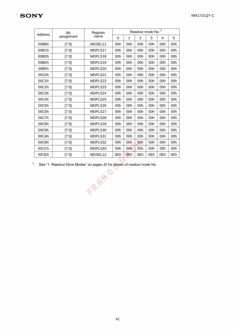
3. Register Setting for Each Readout Drive Mode
The register setting for each readout drive mode available with this sensor is shown in the table below.
Address Bit
assignment Register
name
Readout mode No.*1
0 1 2 3 4 5
0000h
[0] STANDBY 0h
[1] STBLOGIC 0h
[7:2] 01h
0003h
[3:0] STBLVDS 0h 0h 1h 3h 0h 3h
[6:4] CHSEL 0h 0h 1h 3h 0h 3h
[7] 0h
0004h [7:0] MDSEL1 00h 00h 80h 80h 80h 89h
0005h [7:0] MDSEL2 07h 01h 47h 47h 41h 4Dh
0006h [7:0] MDSEL3 00h 00h 00h 00h 00h 00h
0007h [7:0] MDSEL4 00h 00h 00h 00h 00h 00h
000Dh [7:0] SVR According to exposure time
000Eh [7:0]
001Ah [0] MDVREV 0h: vertical direction normal/1h:inverted
[7:1] 00h
0026h [7:0] MDSEL13 74h 74h 74h 74h 74h 74h
0027h [7:0] MDSEL14 74h 74h 74h 74h 74h 74h
0028h [7:0] MDSEL15 74h 74h 74h 74h 74h 74h
007Eh [7:0] MDSEL5 0120h 0120h 0120h 0120h 0120h 0120h
007Fh [7:0]
0080h [7:0] MDPLS01 00h 00h 00h 00h 00h 00h
0081h [7:0] MDPLS02 00h 00h 00h 00h 00h 00h
0082h [7:0] MDPLS03 00h 00h 00h 00h 00h 00h
0083h [7:0] MDPLS04 00h 00h 00h 00h 00h 00h
0084h [7:0] MDPLS05 00h 00h 00h 00h 00h 00h
0085h [7:0] MDPLS06 00h 00h 00h 00h 00h 00h
0086h [7:0] MDPLS07 00h 00h 00h 00h 00h 00h
0087h [7:0] MDPLS08 00h 00h 00h 00h 00h 00h
0095h [7:0] MDPLS09 00h 00h 00h 00h 00h 00h
0096h [7:0] MDPLS10 00h 00h 00h 00h 00h 00h
0097h [7:0] MDPLS11 00h 00h 00h 00h 00h 00h
0098h [7:0] MDPLS12 00h 00h 00h 00h 00h 00h
0099h [7:0] MDPLS13 00h 00h 00h 00h 00h 00h
009Ah [7:0] MDPLS14 00h 00h 00h 00h 00h 00h
009Bh [7:0] MDPLS15 00h 00h 00h 00h 00h 00h
009Ch [7:0] MDPLS16 00h 00h 00h 00h 00h 00h
00B6h [7:0] MDSEL6 47h 47h 47h 47h 47h 67h
00B7h [7:0] MDSEL7 00h 00h 00h 00h 00h 00h
00B8h [7:0] MDSEL8 00h 00h 00h 00h 00h 00h
00B9h [7:0] MDSEL9 00h 00h 00h 00h 00h 00h
00BAh [7:0] MDSEL10 00h 00h 00h 00h 00h 00h
FRAMOS G
MBH
Page 41
IMX172LQT-C
41
Address Bit
assignment Register
name
Readout mode No.*1
0 1 2 3 4 5
00BBh [7:0] MDSEL11 00h 00h 00h 00h 00h 00h
00BCh [7:0] MDPLS17 00h 00h 00h 00h 00h 00h
00BDh [7:0] MDPLS18 00h 00h 00h 00h 00h 00h
00BEh [7:0] MDPLS19 00h 00h 00h 00h 00h 00h
00BFh [7:0] MDPLS20 00h 00h 00h 00h 00h 00h
00C0h [7:0] MDPLS21 00h 00h 00h 00h 00h 00h
00C1h [7:0] MDPLS22 00h 00h 00h 00h 00h 00h
00C2h [7:0] MDPLS23 00h 00h 00h 00h 00h 00h
00C3h [7:0] MDPLS24 00h 00h 00h 00h 00h 00h
00C4h [7:0] MDPLS25 00h 00h 00h 00h 00h 00h
00C5h [7:0] MDPLS26 00h 00h 00h 00h 00h 00h
00C6h [7:0] MDPLS27 00h 00h 00h 00h 00h 00h
00C7h [7:0] MDPLS28 00h 00h 00h 00h 00h 00h
00C8h [7:0] MDPLS29 00h 00h 00h 00h 00h 00h
00C9h [7:0] MDPLS30 00h 00h 00h 00h 00h 00h
00CAh [7:0] MDPLS31 00h 00h 00h 00h 00h 00h
00CBh [7:0] MDPLS32 00h 00h 00h 00h 00h 00h
00CCh [7:0] MDPLS33 00h 00h 00h 00h 00h 00h
00CEh [7:0] MDSEL12 0Eh 0Eh 0Eh 0Eh 0Eh 0Eh
*1 See “1. Readout Drive Modes” on pages 42 for details of readout mode No.
FRAMOS G
MBH
Page 42
IMX172LQT-C
42
Readout Drive Modes
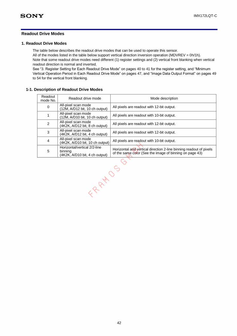
1. Readout Drive Modes
The table below describes the readout drive modes that can be used to operate this sensor.
All of the modes listed in the table below support vertical direction inversion operation (MDVREV = 0h/1h).
Note that some readout drive modes need different (1) register settings and (2) vertical front blanking when vertical
readout direction is normal and inverted.
See “3. Register Setting for Each Readout Drive Mode” on pages 40 to 41 for the register setting, and “Minimum
Vertical Operation Period in Each Readout Drive Mode” on pages 47, and “Image Data Output Format” on pages 49
to 54 for the vertical front blanking.
1-1. Description of Readout Drive Modes
Readout mode No.
Readout drive mode Mode description
0 All-pixel scan mode (12M, A/D12 bit, 10 ch output)
All pixels are readout with 12-bit output.
1 All-pixel scan mode (12M, A/D10 bit, 10 ch output)
All pixels are readout with 10-bit output.
2 All-pixel scan mode (4K2K, A/D12 bit, 8 ch output)
All pixels are readout with 12-bit output.
3 All-pixel scan mode (4K2K, A/D12 bit, 4 ch output)
All pixels are readout with 12-bit output.
4 All-pixel scan mode (4K2K, A/D10 bit, 10 ch output)
All pixels are readout with 10-bit output.
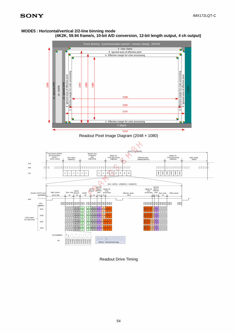
5 Horizontal/vertical 2/2-line binning (4K2K, A/D10 bit, 4 ch output)
Horizontal and vertical direction 2-line binning readout of pixels of the same color (See the image of binning on page 43)
FRAMOS G
MBH
Page 43
IMX172LQT-C
43
1-2. Relationship between Arithmetic Processing and the Number of Output Bits in Each Readout Drive Mode
The table below shows the relationship between the A/D conversion resolution, number of binning pixels, internal
arithmetic processing, and number of output bits in each readout mode.
Note that the number of output bits differs in each mode. In addition the number of output bits is 10 bits, so the
weight of 1 digit is 4 times greater than that during 12-bit output.
Relationship between Arithmetic Processing and the Number of Output Bits in Each Readout Drive Mode
Readout mode No.
A/D conversion resolution
Horizontal pixel
processing
Vertical pixel processing
Total number of binning
pixels
Internal arithmetic processing
Number of output bits
0 12 bits — — — — 12 bits
1 10 bits — — — — 10 bits
2 12 bits — — — — 12 bits
3 12 bits — — — — 12 bits
4 10 bits — — — — 10 bits
5 10 bits 2 binning 2 binning 4 pixels 1/4 10 bits + 2 bits *1
*1
Division is performed by internal arithmetic processing, then the results are output in 12 bits with the integer
item in the upper 10 bits and the decimal item in the lower 2 bits.
B Gb
Gr R
BGb
GrR
BGb
GrR
B Gb
Gr R
B1Gb1
Gr1R1
B2Gb2
Gr2R2
B Gb
Gr R
B3Gb3
Gr3R3
B4Gb4
Gr4R4
R’ Gr’
Gb’ B’
R' = (R1 + R2 + R3 + R4) / 4Gr' = (Gr1 + Gr2 + Gr3 + Gr4) / 4Gb' = (Gb1 + Gb2 + Gb3 + Gb4) / 4B' = (B1 + B2 + B3 + B4) / 4
Horizontal/Vertical 2/2-line Binning Image
FRAMOS G
MBH
Page 44
IMX172LQT-C
44
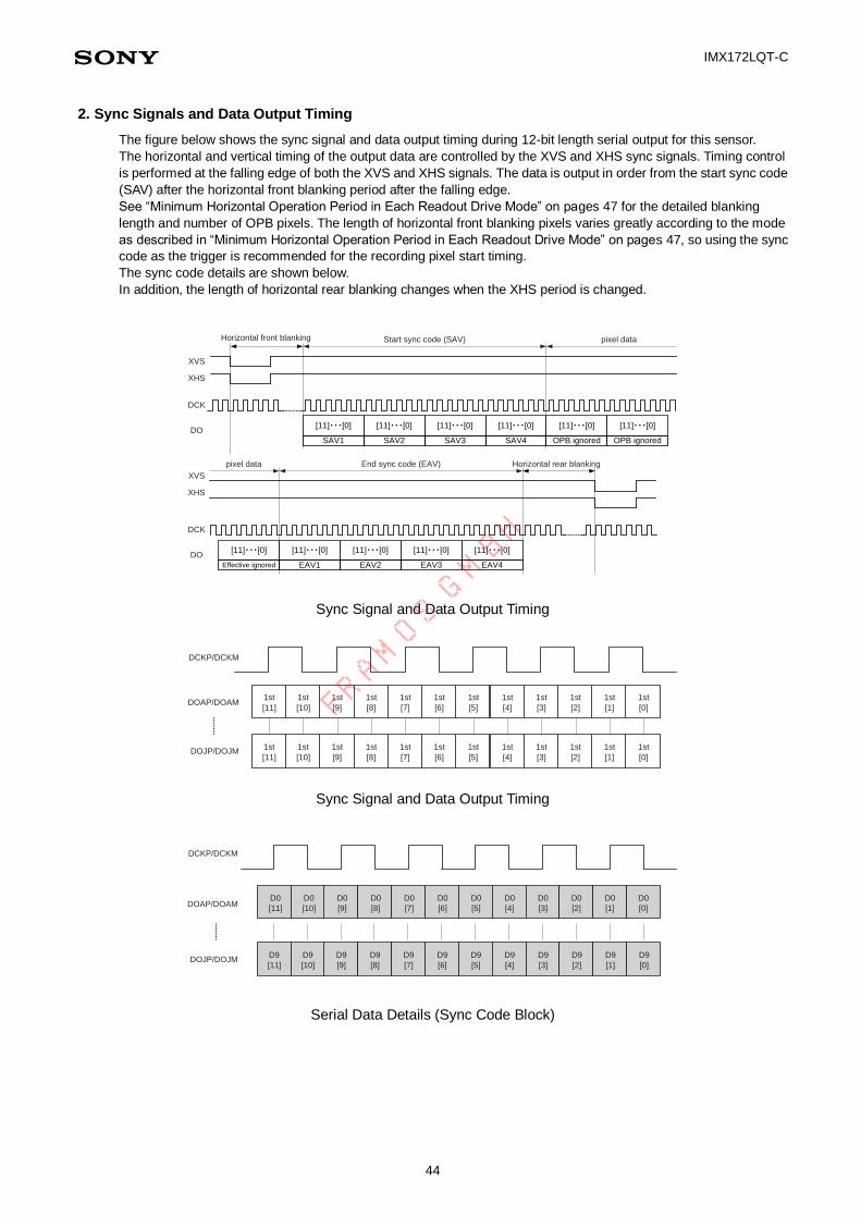
2. Sync Signals and Data Output Timing
The figure below shows the sync signal and data output timing during 12-bit length serial output for this sensor.
The horizontal and vertical timing of the output data are controlled by the XVS and XHS sync signals. Timing control
is performed at the falling edge of both the XVS and XHS signals. The data is output in order from the start sync code
(SAV) after the horizontal front blanking period after the falling edge.
See “Minimum Horizontal Operation Period in Each Readout Drive Mode” on pages 47 for the detailed blanking
length and number of OPB pixels. The length of horizontal front blanking pixels varies greatly according to the mode
as described in “Minimum Horizontal Operation Period in Each Readout Drive Mode” on pages 47, so using the sync
code as the trigger is recommended for the recording pixel start timing.
The sync code details are shown below.
In addition, the length of horizontal rear blanking changes when the XHS period is changed.
XVS
DO
DCK
Horizontal rear blankingEnd sync code (EAV)pixel data
XHS
[11]・・・[0][11]・・・[0][11]・・・[0][11]・・・[0][11]・・・[0]
Effective ignored
XVS
DO
DCK
XHS
EAV1 EAV2 EAV3 EAV4
[11]・・・[0]
SAV1
Horizontal front blanking Start sync code (SAV) pixel data
[11]・・・[0]
SAV2
[11]・・・[0]
SAV3
[11]・・・[0]
SAV4
[11]・・・[0]
OPB ignored
[11]・・・[0]
OPB ignored
Sync Signal and Data Output Timing
DCKP/DCKM
DOJP/DOJM
DOAP/DOAM1st
[11]
1st
[10]
1st
[9]
1st
[8]
1st
[7]
1st
[6]
1st
[5]
1st
[4]
1st
[3]
1st
[2]
1st
[1]
1st
[0]
1st
[11]
1st
[10]
1st
[9]
1st
[8]
1st
[7]
1st
[6]
1st
[5]
1st
[4]
1st
[3]
1st
[2]
1st
[1]
1st
[0]
Sync Signal and Data Output Timing
DCKP/DCKM
DOJP/DOJM
D0
[11]
D0
[10]
D0
[9]
D0
[8]
D0
[7]
D0
[6]
D0
[5]
D0
[4]
D0
[3]
D0
[2]
D0
[1]
D0
[0]
D9
[11]
D9
[10]
D9
[9]
D9
[8]
D9
[7]
D9
[6]
D9
[5]
D9
[4]
D9
[3]
D9
[2]
D9
[1]
D9
[0]
DOAP/DOAM
Serial Data Details (Sync Code Block)
FRAMOS G
MBH
Page 45
IMX172LQT-C
45
Sync code details
LVDS output bit No. Sync code (4 words)
12-bit output 10-bit output 1st word 2nd word 3rd word 4th word
11 9 1 0 0 1
10 8 1 0 0 0
9 7 1 0 0 V 1: Blanking line
0: Except blanking line
8 6 1 0 0 H 1: End sync code
0: Start sync code
7 5 1 0 0 P3
Protection bits 6 4 1 0 0 P2
5 3 1 0 0 P1
4 2 1 0 0 P0
3 1 1 0 0 0
2 0 1 0 0 0
1 — 1 0 0 0
0 — 1 0 0 0
Protection bits
V H P3 P2 P1 P0
0 0 0 0 0 0
0 1 1 1 0 1
1 0 1 0 1 1
1 1 0 1 1 0
Sync code details (hexadecimal notation) 12-bit output
1st word 2nd word 3rd word 4th word
Blanking line Start sync code (SAV)
FFFh 000h 000h
AB0h
End sync code (EAV) B60h
Except blanking line Start sync code (SAV) 800h
End sync code (EAV) 9D0h
Sync code details (hexadecimal notation) 10-bit output
1st word 2nd word 3rd word 4th word
Blanking line Start sync code (SAV)
3FFh 000h 000h
2 ACh
End sync code (EAV) 2D8h
Except blanking line Start sync code (SAV) 200h
End sync code (EAV) 274h
FRAMOS G
MBH
Page 46
IMX172LQT-C
46
3. Output Range of LVDS Output Data
The table below shows the decimal point position, output bit length and output range of the output data in each
readout mode. Note that the value of the first word of the sync code (3FFh, FFFh) and the maximum data value do
not overlap in any readout mode.
Data output range in each readout mode
Readout
mode No.
LVDS output
Decimal point position Output bit length [bit] Output range [hex]
0 2 12 001h to FFEh
1 0 10 001h to 3FEh
2 2 12 001h to FFEh
3 2 12 001h to FFEh
4 0 10 001h to 3FEh
5 2 12 001h to FFEh
Output value during horizontal blanking period is fixed to Low (all 0).
Horizontal sync signal
SAV EAV
[Horizontal blanking]
Fixed Low
[Pixel data]
12 bits: 001h to FFEh
10 bits: 001h to 3FEh
[Horizontal blanking]
Fixed Low
Horizontal blankingPixel dataHorizontal blanking
Readout Drive Timing
FRAMOS G
MBH
Page 47
IMX172LQT-C
47
4. Detailed Specification of Each Mode
(1) Minimum Horizontal/Vertical Operation Period in Each Readout Drive Mode
Minimum Horizontal Operation Period in Each Readout Drive Mode
Readout mode No.
Data rate [MHz]
Horizontal front
blanking [DCK]
*2 *3
Minimum horizontal operation period (Number of pixels conversion)
XHS minimum
period [INCK]
*2
Front OPB
Front effective
pixel margin
Recommended recording pixels
Rear effective
pixel margin
Rear OPB
0 576
(288DDR*1
) 348 to 353 96 36 4000 36 0 644
1 576
(288DDR*1
) 348 to 353 96 36 4000 36 0 536
2 576
(288DDR*1
) 348 to 353 96 28 4096 28 0 811
3 576
(288DDR*1
) 348 to 353 96 28 4096 28 0 1608
4 576
(288DDR*1
) 348 to 353 96 28 4096 28 0 546
5 576
(288DDR*1
) 354 to 359 48 14 2048 14 0 407
*1 DDR : Double Data Rate
*2 If XHS period is shorter than the (XHS minimum period + horizontal front blanking), the data from the previous line may be
output during the horizontal front blanking period. *3
Number of LVDS output signal DCK clock
Minimum Vertical Operation Period in Each Readout Drive Mode
Readout
mode No.
Number of lines per minimum vertical operation period (output data 1H conversion) XVS
minimum
period
[XHS]
Vertical front
blanking
Front
OPB
Front
effective
pixel margin
Recommended
recording pixels
Rear effective
pixel margin
Rear
OPB
0 17
*1
16*2
16 24 3000 22 0 3079
1 17
*1
16*2
16 24 3000 22 0 3079
2 17
*1
16*2
8 10 2160 4 0 2199
3 17
*1
16*2
8 10 2160 4 0 2199
4 17
*1
16*2
8 10 2160 4 0 2199
5 9 (20XHS) 4 10 1080 4 0 2216
*1 When vertical direction normal readout
*2 When vertical direction inverted readout
FRAMOS G
MBH
Page 48
IMX172LQT-C
48
(2) Recommended Horizontal/Vertical Operation Period in Each Readout Drive Mode
Recommended H Period and V Periods
Readout
mode
No.
XHS
period
(INCK) *1
H period
(number
of XHS
pulses) *2
V period
(number
of XHS
pulses)
Frame
frequency
[frame/s]
0 660 1 3120 34.97
1 585 1 3080 39.96
2 1092 1 2200 29.97
3 2184 1 2200 14.99
4 546 1 2200 59.94
5 528 2 2275 59.94
*1 Number of INCK conversion clocks
*2 Number of XHS pulses required to output the data for one sensor line
Imaging Conditions in Each Readout Drive Mode
Readout
mode No.
Imaging conditions
Data rate
[MHz]
Number of
LVDS
output
channels
[ch]
Number of
A/D
conversion
bits
[bit]
Output
data bit
length
[bit]
Number of
horizontal
recording
pixels
Number of
vertical
recording
pixels
Number of
recording
pixels
0 576
(288DDR) 10 12 12 4000 3000 12.00 M pixels
1 576
(288DDR) 10 10 10 4000 3000 12.00 M pixels
2 576
(288DDR) 8 12 12 4096 2160 8.85 M pixels
3 576
(288DDR) 4 12 12 4096 2160 8.85 M pixels
4 576
(288DDR) 10 10 10 4096 2160 8.85 M pixels
5 576
(288DDR) 4 10 12 2048 1080 2.21 M pixels
FRAMOS G
MBH
Page 49
IMX172LQT-C
49
5. Image Data Output Format
The output format in each readout drive mode is as follows.
MODE0 : All-pixel scan mode (12M, 34.97 frame/s, 12-bit A/D conversion, 12-bit length output, 10 ch output)
Front dummy (communication period + sensor clamp)
17XHS (When vertical direction normal readout), 16XHS (When vertical direction inverted readout)
V blank
18 Effective margin for color processing
18 Effective margin for color processing
24
Ign
ore
d O
PB
24
Ign
ore
d O
PB
24
Ign
ore
d a
rea
of e
ffe
ctive
pix
el
12
Effe
ctive
ma
rgin
fo
r co
lor
pro
ce
ssin
g
24
Ign
ore
d a
rea
of e
ffe
ctive
pix
el
48
HO
PB
H b
lan
k
12
Effe
ctive
ma
rgin
fo
r co
lor
pro
ce
ssin
g
4 Ignored area of effective pixel
16 User clamp
4168
30
00
30
36
4024
4000
4072
30
46
30
62
6 Ignored area of effective pixel *1
*1 When vertical direction normal readout : 1 shaded area, 5 aperture area
When vertical direction inverted readout : 6 aperture area
Readout Pixel Image Diagram (4000 × 3000)
Readout Drive Timing
XVS
XHS
DO 0 1 14
15
16
17
20
21
22
23
38
39
40
41
3038
3039
3040
3041
3056
3057
3058
3059
3060
3061
Number of DCK clock
[@288MHz] 6
XHS
DCK
(288MHz)
DOA
EA
V1
EA
V2
EA
V3
EA
V4
SA
V1
SA
V2
SA
V3
SA
V4
0 10
20
30
40
50
60
70
80
90
100
110
120
130
140
150
160
4100
4110
4120
4130
4140
4150
4160
EA
V1
EA
V2
EA
V3
EA
V4
DOB
EA
V1
EA
V2
EA
V3
EA
V4
SA
V1
SA
V2
SA
V3
SA
V4
1 11
21
31
41
51
61
71
81
91
101
111
121
131
141
151
161
4101
4111
4121
4131
4141
4151
4161
EA
V1
EA
V2
EA
V3
EA
V4
DOC
EA
V1
EA
V2
EA
V3
EA
V4
SA
V1
SA
V2
SA
V3
SA
V4
2 12
22
32
42
52
62
72
82
92
102
112
122
132
142
152
162
4102
4112
4122
4132
4142
4152
4162
EA
V1
EA
V2
EA
V3
EA
V4
DOD
EA
V1
EA
V2
EA
V3
EA
V4
SA
V1
SA
V2
SA
V3
SA
V4
3 13
23
33
43
53
63
73
83
93
103
113
123
133
143
153
163
4103
4113
4123
4133
4143
4153
4163
EA
V1
EA
V2
EA
V3
EA
V4
DOE
EA
V1
EA
V2
EA
V3
EA
V4
SA
V1
SA
V2
SA
V3
SA
V4
4 14
24
34
44
54
64
74
84
94
104
114
124
134
144
154
164
4104
4114
4124
4134
4144
4154
4164
EA
V1
EA
V2
EA
V3
EA
V4
DOF
EA
V1
EA
V2
EA
V3
EA
V4
SA
V1
SA
V2
SA
V3
SA
V4
5 15
25
35
45
55
65
75
85
95
105
115
125
135
145
155
165
4105
4115
4125
4135
4145
4155
4165
EA
V1
EA
V2
EA
V3
EA
V4
DOG
EA
V1
EA
V2
EA
V3
EA
V4
SA
V1
SA
V2
SA
V3
SA
V4
6 16
26
36
46
56
66
76
86
96
106
116
126
136
146
156
166
4106
4116
4126
4136
4146
4156
4166
EA
V1
EA
V2
EA
V3
EA
V4
DOH
EA
V1
EA
V2
EA
V3
EA
V4
SA
V1
SA
V2
SA
V3
SA
V4
7 17
27
37
47
57
67
77
87
97
107
117
127
137
147
157
167
4107
4117
4127
4137
4147
4157
4167
EA
V1
EA
V2
EA
V3
EA
V4
DOI
EA
V1
EA
V2
EA
V3
EA
V4
SA
V1
SA
V2
SA
V3
SA
V4
8 18
28
38
48
58
68
78
88
98
108
118
128
138
148
158
168
4108
4118
4128
4138
4148
4158
4168
EA
V1
EA
V2
EA
V3
EA
V4
DOJ
EA
V1
EA
V2
EA
V3
EA
V4
SA
V1
SA
V2
SA
V3
SA
V4
9 19
29
39
49
59
69
79
89
99
109
119
129
139
149
159
169
4109
4119
4129
4139
4149
4159
4169
EA
V1
EA
V2
EA
V3
EA
V4
24 2430 12 12 12
LVDS output
10ch 12bit serial
18 2400 12348 to 353
SA
V[9
]
SA
V[8
]
SA
V[7
]
SA
V[6
]
SA
V[5
]
SA
V[4
]
SA
V[3
]
SA
V[2
]
SA
V[1
]
SA
V[0
]
6[DCK] *Detected both edge.
SA
V[1
1]
SA
V[1
0]
DCK(288MHz)
DO
Sync codeHBLK period
*1 17XHS : When vertical direction normal readout
16XHS : When vertical direction inverted readout
*2 41XHS : When vertical direction normal readout
42XHS : When vertical direction inverted readout
HOPB
ignored
1[H] = 1[XHS] = 660[INCK] = 2640[DCK]
HOPB
HOPB
ignored
Ignored
area of
effective
pixel
Margin for
Color
processing Effective pixels
Margin for
Color
processing
Ignored
area of
effective
pixel Sync code
Front dummy
[Communication
period +
sensor clamp] *1
User clamp
16H[16XHS]
Ignored area
of effective
pixel
6H[6XHS]
Margin for
Color processing
18H[18XHS]
Effective pixels
3000H[3000XHS]
1[XVS] = 3120[XHS]
Margin for
Color processing
18H[18XHS]
Ignored area
of effective
pixel
4H[4XHS]
VBLK
period *2
FRAMOS G
MBH
Page 50
IMX172LQT-C
50
MODE1 : All-pixel scan mode (12M, 39.96 frame/s, 10-bit A/D conversion, 10-bit length output, 10 ch output)
Front dummy (communication period + sensor clamp)
17XHS (When vertical direction normal readout), 16XHS (When vertical direction inverted readout)
V blank
18 Effective margin for color processing
18 Effective margin for color processing
24
Ign
ore
d O
PB
24
Ign
ore
d O
PB
24
Ign
ore
d a
rea
of e
ffe
ctive
pix
el
12
Effe
ctive
ma
rgin
fo
r co
lor
pro
ce
ssin
g
24
Ign
ore
d a
rea
of e
ffe
ctive
pix
el
48
HO
PB
H b
lan
k
12
Effe
ctive
ma
rgin
fo
r co
lor
pro
ce
ssin
g
4 Ignored area of effective pixel
16 User clamp
4168
30
00
30
36
4024
4000
4072
30
46
30
62
6 Ignored area of effective pixel *1
*1 When vertical direction normal readout : 1 shaded area, 5 aperture area
When vertical direction inverted readout : 6 aperture area
Readout Pixel Image Diagram (4000 × 3000)
Readout Drive Timing
XVS
XHS
DO 0 1 14
15
16
17
20
21
22
23
38
39
40
41
3038
3039
3040
3041
3056
3057
3058
3059
3060
3061
Number of DCK clock
[@288MHz] 5
XHS
DCK
(288MHz)
DOA
EA
V1
EA
V2
EA
V3
EA
V4
SA
V1
SA
V2
SA
V3
SA
V4
0 10
20
30
40
50
60
70
80
90
100
110
120
130
140
150
160
4100
4110
4120
4130
4140
4150
4160
EA
V1
EA
V2
EA
V3
EA
V4
DOB
EA
V1
EA
V2
EA
V3
EA
V4
SA
V1
SA
V2
SA
V3
SA
V4
1 11
21
31
41
51
61
71
81
91
101
111
121
131
141
151
161
4101
4111
4121
4131
4141
4151
4161
EA
V1
EA
V2
EA
V3
EA
V4
DOC
EA
V1
EA
V2
EA
V3
EA
V4
SA
V1
SA
V2
SA
V3
SA
V4
2 12
22
32
42
52
62
72
82
92
102
112
122
132
142
152
162
4102
4112
4122
4132
4142
4152
4162
EA
V1
EA
V2
EA
V3
EA
V4
DOD
EA
V1
EA
V2
EA
V3
EA
V4
SA
V1
SA
V2
SA
V3
SA
V4
3 13
23
33
43
53
63
73
83
93
103
113
123
133
143
153
163
4103
4113
4123
4133
4143
4153
4163
EA
V1
EA
V2
EA
V3
EA
V4
DOE
EA
V1
EA
V2
EA
V3
EA
V4
SA
V1
SA
V2
SA
V3
SA
V4
4 14
24
34
44
54
64
74
84
94
104
114
124
134
144
154
164
4104
4114
4124
4134
4144
4154
4164
EA
V1
EA
V2
EA
V3
EA
V4
DOF
EA
V1
EA
V2
EA
V3
EA
V4
SA
V1
SA
V2
SA
V3
SA
V4
5 15
25
35
45
55
65
75
85
95
105
115
125
135
145
155
165
4105
4115
4125
4135
4145
4155
4165
EA
V1
EA
V2
EA
V3
EA
V4
DOG
EA
V1
EA
V2
EA
V3
EA
V4
SA
V1
SA
V2
SA
V3
SA
V4
6 16
26
36
46
56
66
76
86
96
106
116
126
136
146
156
166
4106
4116
4126
4136
4146
4156
4166
EA
V1
EA
V2
EA
V3
EA
V4
DOH
EA
V1
EA
V2
EA
V3
EA
V4
SA
V1
SA
V2
SA
V3
SA
V4
7 17
27
37
47
57
67
77
87
97
107
117
127
137
147
157
167
4107
4117
4127
4137
4147
4157
4167
EA
V1
EA
V2
EA
V3
EA
V4
DOI
EA
V1
EA
V2
EA
V3
EA
V4
SA
V1
SA
V2
SA
V3
SA
V4
8 18
28
38
48
58
68
78
88
98
108
118
128
138
148
158
168
4108
4118
4128
4138
4148
4158
4168
EA
V1
EA
V2
EA
V3
EA
V4
DOJ
EA
V1
EA
V2
EA
V3
EA
V4
SA
V1
SA
V2
SA
V3
SA
V4
9 19
29
39
49
59
69
79
89
99
109
119
129
139
149
159
169
4109
4119
4129
4139
4149
4159
4169
EA
V1
EA
V2
EA
V3
EA
V4
2025 10 10 10
LVDS output
10ch 10bit serial
15 2000 10348 to 353 20
DCK(288MHz)
DO
Sync codeHBLK period
*1 17XHS : When vertical direction normal readout
16XHS : When vertical direction inverted readout
*2 1XHS : When vertical direction normal readout
2XHS : When vertical direction inverted readout
HOPB
ignored
1[H] = 1[XHS] = 585[INCK] = 2340[DCK]
HOPB
HOPB
ignored
Ignored
area of
effective
pixel
Margin for
Color
processing Effective pixels
Margin for
Color
processing
Ignored
area of
effective
pixel Sync code
Front dummy
[Communication
period +
sensor clamp] *1
User clamp
16H[16XHS]
Ignored area
of effective
pixel
6H[6XHS]
Margin for
Color processing
18H[18XHS]
Effective pixels
3000H[3000XHS]
1[XVS] = 3080[XHS]
Margin for
Color processing
18H[18XHS]
Ignored area
of effective
pixel
4H[4XHS]
VBLK
period *2
SA
V[9
]
SA
V[8
]
SA
V[7
]
SA
V[6
]
SA
V[5
]
SA
V[4
]
SA
V[3
]
SA
V[2
]
SA
V[1
]
SA
V[0
]
5[DCK] *Detected both edge.
FRAMOS G
MBH
Page 51
IMX172LQT-C
51
MODE2 : All-pixel scan mode (4K2K, 29.97 frame/s, 12-bit A/D conversion, 12-bit length output, 8 ch output)
Front dummy (communication period + sensor clamp)
17XHS(When vertical direction normal readout), 16XHS(When vertical direction inverted readout)
V blank
4 Effective margin for color processing
4 Effective margin for color processing
24
Ign
ore
d O
PB
24
Ign
ore
d O
PB
16
Ign
ore
d a
rea
of e
ffe
ctive
pix
el
12
Effe
ctive
ma
rgin
fo
r co
lor
pro
ce
ssin
g
16
Ign
ore
d a
rea
of e
ffe
ctive
pix
el
48
HO
PB
H b
lan
k
12
Effe
ctive
ma
rgin
fo
r co
lor
pro
ce
ssin
g
8 User clamp
4248
21
60
21
68
4120
4096
4152
21
74
21
82
6 Ignored area of effective pixel *1
*1 When vertical direction normal readout : 1 shaded area, 5 aperture area
When vertical direction inverted readout : 6 aperture area
Readout Pixel Image Diagram (4096 × 2160)
Readout Drive Timing
XVS
XHS
DO 0 1 6 7 8 9 12
13
14
15
16
17
18
19
2176
2177
2178
2179
2180
2181
Number of DCK clock
[@288MHz] 6
XHS
DCK
(288MHz)
DOA
SA
V1
SA
V2
SA
V3
SA
V4
0 8 16
24
32
40
64
72
80
88
96
104
112
120
128
4200
4208
4216
4224
4232
4240
EA
V1
EA
V2
EA
V3
EA
V4
DOB
SA
V1
SA
V2
SA
V3
SA
V4
1 9 17
25
33
41
65
73
81
89
97
105
113
121
129
4201
4209
4217
4225
4233
4241
EA
V1
EA
V2
EA
V3
EA
V4
DOC
SA
V1
SA
V2
SA
V3
SA
V4
2 10
18
26
34
42
66
74
82
90
98
106
114
122
130
4202
4210
4218
4226
4234
4242
EA
V1
EA
V2
EA
V3
EA
V4
DOE
SA
V1
SA
V2
SA
V3
SA
V4
3 11
19
27
35
43
67
75
83
91
99
107
115
123
131
4203
4211
4219
4227
4235
4243
EA
V1
EA
V2
EA
V3
EA
V4
DOF
SA
V1
SA
V2
SA
V3
SA
V4
4 12
20
28
36
44
68
76
84
92
100
108
116
124
132
4204
4212
4220
4228
4236
4244
EA
V1
EA
V2
EA
V3
EA
V4
DOH
SA
V1
SA
V2
SA
V3
SA
V4
5 13
21
29
37
45
69
77
85
93
101
109
117
125
133
4205
4213
4221
4229
4237
4245
EA
V1
EA
V2
EA
V3
EA
V4
DOI
SA
V1
SA
V2
SA
V3
SA
V4
6 14
22
30
38
46
70
78
86
94
102
110
118
126
134
4206
4214
4222
4230
4238
4246
EA
V1
EA
V2
EA
V3
EA
V4
DOJ
SA
V1
SA
V2
SA
V3
SA
V4
7 15
23
31
39
47
71
79
87
95
103
111
119
127
135
4207
4215
4223
4231
4239
4247
EA
V1
EA
V2
EA
V3
EA
V4
1212 24
LVDS output
8ch 12bit serial
348 to 353 24 18 3072 121836
SA
V[9
]
SA
V[8
]
SA
V[7
]
SA
V[6
]
SA
V[5
]
SA
V[4
]
SA
V[3
]
SA
V[2
]
SA
V[1
]
SA
V[0
]
6[DCK] *Detected both edge.
SA
V[1
1]
SA
V[1
0]
DCK(288MHz)
DO
Sync codeHBLK period
*1 17XHS : When vertical direction normal readout
16XHS : When vertical direction inverted readout
*2 1XHS : When vertical direction normal readout
2XHS : When vertical direction inverted readout
HOPBignored
1[H] = 1[XHS] = 1092[INCK] = 4368[DCK]
HOPB
HOPBignored
Ignoredarea of
effectivepixel
Margin forColor
processing Effective pixels
Margin forColor
processing
Ignoredarea of
effectivepixel Sync code
Front dummy[Communication
period +sensor clamp] *1
User clamp8H[8XHS]
Ignored areaof effective
pixel6H[6XHS]
Margin forColor processing
4H[4XHS]Effective pixels
2160H[2160XHS]
1[XVS] = 2200[XHS]
Margin forColor processing
4H[4XHS]VBLK
period *2
HBLK period
FRAMOS G
MBH
Page 52
IMX172LQT-C
52
MODE3: All-pixel scan mode (4K2K, 14.99 frame/s, 12-bit A/D conversion, 12-bit length output, 4 ch output)
Front dummy (communication period + sensor clamp)
17XHS(When vertical direction normal readout), 16XHS(When vertical direction inverted readout)
V blank
4 Effective margin for color processing
4 Effective margin for color processing
24
Ign
ore
d O
PB
24
Ign
ore
d O
PB
16
Ign
ore
d a
rea
of e
ffe
ctive
pix
el
12
Effe
ctive
ma
rgin
fo
r co
lor
pro
ce
ssin
g
16
Ign
ore
d a
rea
of e
ffe
ctive
pix
el
48
HO
PB
H b
lan
k
12
Effe
ctive
ma
rgin
fo
r co
lor
pro
ce
ssin
g
8 User clamp
4248
21
60
21
68
4120
4096
4152
21
74
21
82
6 Ignored area of effective pixel *1
*1 When vertical direction normal readout : 1 shaded area, 5 aperture area
When vertical direction inverted readout : 6 aperture area
Readout Pixel Image Diagram (4096 × 2160)
Readout Drive Timing
XVS
XHS
DO 0 1 6 7 8 9 12
13
14
15
16
17
18
19
2176
2177
2178
2179
2180
2181
Number of DCK clock
[@288MHz] 18 18 24
XHS
DCK
(288MHz)
DOC
SA
V1
SA
V2
SA
V3
SA
V4
0 20
24
68
72
92
96
108
112
116
120
124
4216
4220
4224
4228
4232
4244
EA
V1
EA
V2
EA
V3
EA
V4
DOE
SA
V1
SA
V2
SA
V3
SA
V4
1 21
25
69
73
93
97
109
113
117
121
125
4217
4221
4225
4229
4233
4245
EA
V1
EA
V2
EA
V3
EA
V4
DOF
SA
V1
SA
V2
SA
V3
SA
V4
2 22
26
70
74
94
98
110
114
118
122
126
4218
4222
4226
4230
4234
4246
EA
V1
EA
V2
EA
V3
EA
V4
DOH
SA
V1
SA
V2
SA
V3
SA
V4
3 23
27
71
75
95
99
111
115
119
123
127
4219
4223
4227
4231
4235
4247
EA
V1
EA
V2
EA
V3
EA
V4
24
LVDS output
4ch 12bit serial
72 36 24348 to 353 24 36 6144
SA
V[9
]
SA
V[8
]
SA
V[7
]
SA
V[6
]
SA
V[5
]
SA
V[4
]
SA
V[3
]
SA
V[2
]
SA
V[1
]
SA
V[0
]
6[DCK] *Detected both edge.
SA
V[1
1]
SA
V[1
0]
DCK(288MHz)
DO
Sync codeHBLK period
*1 17XHS : When vertical direction normal readout
16XHS : When vertical direction inverted readout
*2 1XHS : When vertical direction normal readout
2XHS : When vertical direction inverted readout
HOPBignored
1[H] = 1[XHS] = 2184[INCK] = 8736[DCK]
HOPB
HOPBignored
Ignoredarea of
effectivepixel
Margin forColor
processing Effective pixels
Margin forColor
processing
Ignoredarea of
effectivepixel Sync code
Front dummy[Communication
period +sensor clamp] *1
User clamp8H[8XHS]
Ignored areaof effective
pixel6H[6XHS]
Margin forColor processing
4H[4XHS]Effective pixels
2160H[2160XHS]
1[XVS] = 2200[XHS]
Margin forColor processing
4H[4XHS]VBLK
period *2
HBLK period
FRAMOS G
MBH
Page 53
IMX172LQT-C
53
MODE4: All-pixel scan mode (4K2K, 59.94 frame/s, 10-bit A/D conversion, 10-bit length output, 10 ch output)
Front dummy (communication period + sensor clamp)
17XHS(When vertical direction normal readout), 16XHS(When vertical direction inverted readout)
V blank
4 Effective margin for color processing
4 Effective margin for color processing
24
Ign
ore
d O
PB
24
Ign
ore
d O
PB
16
Ign
ore
d a
rea
of e
ffe
ctive
pix
el
12
Effe
ctive
ma
rgin
fo
r co
lor
pro
ce
ssin
g
16
Ign
ore
d a
rea
of e
ffe
ctive
pix
el
48
HO
PB
H b
lan
k
12
Effe
ctive
ma
rgin
fo
r co
lor
pro
ce
ssin
g
8 User clamp
4248
21
60
21
68
4120
4096
4152
21
74
21
82
6 Ignored area of effective pixel *1
*1 When vertical direction normal readout : 1 shaded area, 5 aperture area
When vertical direction inverted readout : 6 aperture area
Readout Pixel Image Diagram (4096 × 2160)
Readout Drive Timing
XVS
XHS
DO 0 1 6 7 8 9 12
13
14
15
16
17
18
19
2176
2177
2178
2179
2180
2181
Number of DCK clock
[@288MHz] 5 5
XHS
DCK
(288MHz)
DOA
EA
V1
EA
V2
EA
V3
EA
V4
SA
V1
SA
V2
SA
V3
SA
V4
0 10
20
30
40
50
60
70
80
90
100
110
120
130
140
150
4190
4200
4210
4220
4230
4240
EA
V1
EA
V2
EA
V3
EA
V4
DOB
EA
V1
EA
V2
EA
V3
EA
V4
SA
V1
SA
V2
SA
V3
SA
V4
1 11
21
31
41
51
61
71
81
91
101
111
121
131
141
151
4191
4201
4211
4221
4231
4241
EA
V1
EA
V2
EA
V3
EA
V4
DOC
EA
V1
EA
V2
EA
V3
EA
V4
SA
V1
SA
V2
SA
V3
SA
V4
2 12
22
32
42
52
62
72
82
92
102
112
122
132
142
152
4192
4202
4212
4222
4232
4242
EA
V1
EA
V2
EA
V3
EA
V4
DOD
EA
V1
EA
V2
EA
V3
EA
V4
SA
V1
SA
V2
SA
V3
SA
V4
3 13
23
33
43
53
63
73
83
93
103
113
123
133
143
153
4193
4203
4213
4223
4233
4243
EA
V1
EA
V2
EA
V3
EA
V4
DOE
EA
V1
EA
V2
EA
V3
EA
V4
SA
V1
SA
V2
SA
V3
SA
V4
4 14
24
34
44
54
64
74
84
94
104
114
124
134
144
154
4194
4204
4214
4224
4234
4244
EA
V1
EA
V2
EA
V3
EA
V4
DOF
EA
V1
EA
V2
EA
V3
EA
V4
SA
V1
SA
V2
SA
V3
SA
V4
5 15
25
35
45
55
65
75
85
95
105
115
125
135
145
155
4195
4205
4215
4225
4235
4245
EA
V1
EA
V2
EA
V3
EA
V4
DOG
EA
V1
EA
V2
EA
V3
EA
V4
SA
V1
SA
V2
SA
V3
SA
V4
6 16
26
36
46
56
66
76
86
96
106
116
126
136
146
156
4196
4206
4216
4226
4236
4246
EA
V1
EA
V2
EA
V3
EA
V4
DOH
EA
V1
EA
V2
EA
V3
EA
V4
SA
V1
SA
V2
SA
V3
SA
V4
7 17
27
37
47
57
67
77
87
97
107
117
127
137
147
157
4197
4207
4217
4227
4237
4247
EA
V1
EA
V2
EA
V3
EA
V4
DOI
EA
V1
EA
V2
EA
V3
EA
V4
SA
V1
SA
V2
SA
V3
SA
V4
8 18
28
38
48
58
68
78
88
98
108
118
128
138
148
158
4198
4208
4218
4228
4238
EA
V1
EA
V2
EA
V3
EA
V4
DOJ
EA
V1
EA
V2
EA
V3
EA
V4
SA
V1
SA
V2
SA
V3
SA
V4
9 19
29
39
49
59
69
79
89
99
109
119
129
139
149
159
4199
4209
4219
4229
4239
EA
V1
EA
V2
EA
V3
EA
V4
348 to 353 20
LVDS output
10ch 10bit serial
15 10 2025 10 10 2045
SA
V[9
]
SA
V[8
]
SA
V[7
]
SA
V[6
]
SA
V[5
]
SA
V[4
]
SA
V[3
]
SA
V[2
]
SA
V[1
]
SA
V[0
]
5[DCK] *Detected both edge.
DCK(288MHz)
DO
Sync codeHBLK period
*1 17XHS : When vertical direction normal readout
16XHS : When vertical direction inverted readout
*2 1XHS : When vertical direction normal readout
2XHS : When vertical direction inverted readout
data from previous line
HOPBignored
1[H] = 1[XHS] = 546[INCK] = 2184[DCK]
HOPB
HOPBignored
Ignoredarea of
effectivepixel
Margin forColor
processing Effective pixels
Margin forColor
processing
Ignoredarea of
effectivepixel Sync code
Front dummy[Communication
period +sensor clamp] *1
User clamp8H[8XHS]
Ignored areaof effective
pixel6H[6XHS]
Margin forColor processing
4H[4XHS]Effective pixels
2160H[2160XHS]
1[XVS] = 2200[XHS]
Margin forColor processing
4H[4XHS]VBLK
period *2
FRAMOS G
MBH
Page 54
IMX172LQT-C
54
MODE5 : Horizontal/vertical 2/2-line binning mode (4K2K, 59.94 frame/s, 10-bit A/D conversion, 12-bit length output, 4 ch output)
Front dummy (communication period + sensor clamp) 20XHS
4 Effective margin for color processing
4 Effective margin for color processing
12
Ign
ore
d O
PB
12
Ign
ore
d O
PB
8
Ign
ore
d a
rea
of e
ffe
ctive
pix
el
8
Ign
ore
d a
rea
of e
ffe
ctive
pix
el
24
HO
PB
H b
lank
6
Effe
ctive
ma
rgin
fo
r co
lor
pro
ce
ssin
g
4 User clamp
6 Ignored area of effective pixel
2124
10
80
10
88
2060
2048
2076
10
94
10
98
V blank
6
Effe
ctive
ma
rgin
fo
r co
lor
pro
ce
ssin
g
Readout Pixel Image Diagram (2048 × 1080)
Readout Drive Timing
XVS
XHS
DO
Number of DCK clock
[@288MHz] 6
XHS
DCK
(288MHz)
DOC
SA
V1
SA
V2
SA
V3
SA
V4
0 4 8 12
16
28
32
36
40
44
48
52
56
60
64
68
72
2096
2100
2104
2108
2112
2116
2120
EA
V1
EA
V2
EA
V3
EA
V4
DOE
SA
V1
SA
V2
SA
V3
SA
V4
1 5 9 13
17
29
33
37
41
45
49
53
57
61
65
69
73
2097
2101
2105
2109
2113
2117
2121
EA
V1
EA
V2
EA
V3
EA
V4
DOF
SA
V1
SA
V2
SA
V3
SA
V4
2 6 10
14
18
30
34
38
42
46
50
54
58
62
66
70
74
2098
2102
2106
2110
2114
2118
2122
EA
V1
EA
V2
EA
V3
EA
V4
DOH
SA
V1
SA
V2
SA
V3
SA
V4
3 7 11
15
19
31
35
39
43
47
51
55
59
63
67
71
75
2099
2103
2107
2111
2115
2119
2123
EA
V1
EA
V2
EA
V3
EA
V4
LVDS output
4ch 12bit serial
12 3072 12354 to 359 24 18 36 18 12 24
0 1 2 3 4 5 12
13
14
158 9 10
11
1094
1095
1096
1097
1092
1093
SA
V[9
]
SA
V[8
]
SA
V[7
]
SA
V[6
]
SA
V[5
]
SA
V[4
]
SA
V[3
]
SA
V[2
]
SA
V[1
]
SA
V[0
]
6[DCK] *Detected both edge.
SA
V[1
1]
SA
V[1
0]
DCK(288MHz)
DO
Sync codeHBLK periodHOPBignored
1[H] = 2[XHS] = 1056[INCK] = 4224[DCK]
HOPB
HOPBignored
Ignoredarea of
effectivepixel
Margin forColor
processing Effective pixels
Margin forColor
processing
Ignoredarea of
effectivepixel Sync code HBLK period
Front dummy 20XHS[Communication
period +sensor clamp]
User clamp4H[8XHS]
Ignored areaof effective
pixel6H[12XHS]
Margin forColor processing
4H[8XHS]Effective pixels
1080H[2160XHS]
1[XVS] = 2275[XHS]
Margin forColor processing
4H[8XHS]VBLK period
59XHS
FRAMOS G
MBH
Page 55
IMX172LQT-C
55
Integration Time in Each Readout Drive Mode and Mode Changes
1. Integration Time in Each Readout Drive Mode
The integration time for this sensor's output data is set using the electronic shutter timing setting registers SHR, SVR
and SPL. The formulas and constants used to calculate the integration time are shown below.
In addition, the frame rate can be reduced by setting the SVR register to “1” or more.
Integration Time [s] = [{Number of XHS per XVS period × (SVR value – SPL value + 1) – (SHR value)}
× Number of clock per XHS Period + Number of clocks per internal offset period]/INCK
frequency [Hz]
* See the following table for the numbers of clocks per internal offset period.
* See “Electronic Shutter Timing” on page 35 for the SHR register setting range.
Constants Used to Calculate the Integration Time
Readout mode No. 0 1 2 3 4 5
Number of clocks per internal offset period
201 150 201 201 150 150
The figure below shows operation when changing SHR. The V1 and V2 periods in the figure below are two
continuous XVS periods. The SHR value set within the first 6XHS periods (recommended serial communication
period) of V1 is updated internally at the end of the 6XHS periods, and then output data which reflect the new
setting is output in the V2 period. Note that the SHR setting and output are offset by 1XVS period.
Serial
communication
Sensor internal
V drive
6XHS
Valid data outputValid data outputValid data output
XVS
XHS .........
Y
SHR
......
Valid data output
SHR
change
SHR
.. .
RHSRHSRHS
Valid data output
V2 periodV1 period
Output frame
read out
shutter
read out
shutter
read out
shutter
read out
shutter
read out
shutter
shutter
6XHS 6XHS 6XHS 6XHS 6XHS
SHR Change Sequence
FRAMOS G
MBH
Page 56
IMX172LQT-C
56
The vertical sync signal XVS can be subsampled inside the sensor according to the SVR register. The vertical
sync signal cycle is treated as (SVR value + 1) inside the sensor. In addition, the frame rate changes to 1/ (SVR
value + 1) according to the SVR value.
The figure below shows the operation when changing the SVR register. The example in the figure below shows
the update timing when SPL = 0 and the SVR value is changed from “0” to “1”. The SVR value set within the first
6XHS periods (recommended serial communication period) of V2 is updated internally at the end of the 6XHS
periods, and then applied from the shutter operation in the V2 period. Readout operation is not performed in the
V3 period, and output data which reflect the changing of SVR is output in the V4 period.
The image data of the V1 period before the SVR value is changed is output as valid data in the V2 period.
In addition, note that communication is also prohibited during the first 6XHS periods (recommended serial
communication period) of the V3 period (the frame during which readout operation is not performed).
Serialcommunication
Sensor internal V drive
Valid data outputValid data output
V5 period
Valid data output
V4 periodV2 periodV1 period
6XHSXVS
XHS
Output frame
.. .
read out
.. . .. .
Y
SHR
......
shutter
SHR
.. .
SHR
SVR = 0SPL = 0
SVRchanged to “1”
Communicationprohibited
Communicationprohibited
6XHS 6XHS 6XHS 6XHS 6XHS
read out
shutterread out
shutter
shutter
V3 period
SVR Change Sequence
When the internal vertical sync signal is subsampled by the SVR register, the SPL register can be used to set the
shutter in the vertical sync signal subsampling periods (the V2, V4 and V6 periods in the figure below).
The figure below shows the operation when changing the SPL register. The example in the figure below shows the
update timing when SVR = 1 and SPL is changed from “0” to “1”. SVR = 1 and SPL = 0 in the continuous frames of
the V1 and V2 periods, so shutter operation is performed in the V1 period and the corresponding data is output in
the V3 period. (See the aforementioned description of operation when SVR ≥ 1.)
The SPL value set within the first 6XHS periods (recommended serial communication period) of V3 is updated
internally at the end of the 6XHS periods, and then applied from the shutter operation in the V3 and V4 periods.
Readout operation is not performed in the V4 period, and output data which reflect the SPL change is output in the
V5 period. The image data of the V1 and V2 periods before the SPL value is changed is output as valid data in the
V3 period.
In addition, note that communication is also prohibited during the first 6XHS periods (recommended serial
communication period) of the V4 period (the frame during which readout operation is not performed).
The SPL register cannot be used in readout mode No.6: Vertical 2/9 subsampling binning mode (low power
consumption drive), so use the SHR register when setting the shutter in the vertical sync signal subsampling
period.
Serial
communication
Sensor internal
V drive
Output frame
shutter
Valid data output
XVS
XHS
V1 period
......
Y
.. . .. .
Valid data output
.. .
SHR SHR
SPL
changed to “1”
read out
.. .
V3 period
SVR = 1
SPL = 0
SHR
.. .
6XHS6XHS6XHS6XHS6XHS6XHS
Valid data outputValid data output
Communication
prohibitedCommunication
prohibited
V2 period V4 period V5 period V6 period
shutter
read out
read out
read out
shutter
SPL Change Sequence
FRAMOS G
MBH
Page 57
IMX172LQT-C
57
2. Operation when Changing the Readout Drive Mode
One frame of invalid data is always generated when changing the readout drive mode.
In addition to when changing the readout mode setting, this same sequence also results when the vertical direction
readout inversion setting is changed.
The figure below shows the mode transition sequence (Mode A to Mode B). The output data is invalid in the frame
(V1 period) in which the setting is changed to Mode B. Valid data which reflect the new setting is output from the next
frame (V2 period). If the XHS period for Mode A and Mode B differs, change XHS period at the timing shown in the
figure below (V1 head).
In addition, note that when the output data length or the output data rate differ in Mode A and Mode B, the new data
format is output from the start of the 7th XHS of the frame (V1 period) in which the setting is changed to Mode B.
Serial
communication
Sensor internal
V drive
Output frame
6XHS6XHS 6XHS 6XHS
Mode Bdata formatMode AOutput data format
XVS
XHS ......
A shutterY
Mode B
V2 period
Mode B Mode B
SHR
MODE
changed to “B”
SHR
A read out
B shutter
B read out
Mode A Mode A
.. .
SHR
Set the SHR for
MODE = B here.
.. . .. . .. .
SHR SHR SHR
XHS period
change timing
Invalid data output
A shutter
A read out
B shutter
B read out
B shutter
B read out
B shutter
B read out
6XHS6XHS
V1 period
data format
Mode Transition
FRAMOS G
MBH
Page 58
IMX172LQT-C
58
3. Interrupt Mode Change
The sensor mode can be changed using interrupts in all modes.
When changing the mode using an interrupt, the mode can be changed by inputting XVS in sync with XHS after
18XHS periods or more*1
have elapsed from the start of the frame, and transmitting the mode setting register value
within the communication period. In addition, the data output before the interrupt mode change is cut off at the timing
of the interrupt mode change.
Mode A data format
B read out
Mode B data formatOutput data format
XVS
XHS
Serial
communication
Output frame
Sensor internal
V drive
......
A read out
A shutter
A read out
A shutter
Y
Mode B Mode BMode A
SHR
MODEchanged to "B"
SHR
.. .
SHR
Interrupt
timing
Set the SHR for MODE = B here.
......
SHRB shutter
SHR
6XHS 6XHS 6XHS 6XHS 6XHS
18XHS or more
(1XHS increments)
B read out
B shutter
B read out
B shutter
Invalid data output
Interrupt Mode Change
4. Data Clock (DCK) Change Timing
When switching the data clock (DCK) frequency by the output format setting register FREQ, hazard may occur in the
1 clock immediately after it.
Do not use the DCK immediately after the change. Note that normal DCK is output one or before the data start sync
code.
XVS
XHS
DCK
DATACommunication period
6XHS Undetermined
1 clk
Normal
DCK ≥ 1 clk1st 2nd 3rd 4th
Sync code (SAV)
DCK Change Period
FRAMOS G
MBH
Page 59
IMX172LQT-C
59
Power-on/off Sequence
1. Power-on Sequence
VDDD1 (1.2 V) 0.8 × VDDD1
Reset signal
XCLR
≥ 100 ns
3-wire serial input signals
XCE/SCK/SDI
Sync signal input signals
XVS/XHS
VDDD2 (1.8 V)
VADD (2.8 V)
0.8 × VDDD2
0.8 × VADD
≥ 100 ns
≥ 0 μs
Master clock
INCK
Status (1) (2)
≥ 100 ns
≥ 100 ns
≥ 0 μs
* INCK must not be over VDDD2
Power-on Sequence
Period name Remarks
(1) Power stabilization time
All input signals are at Low level.
There are no constraints of the power-on sequence with VADD,
VDDD1, VDDD2.
(2) Standby cancel register
communication
Start the standby cancel sequence after the last power supply in
VADD, VDDD1, VDDD2.
FRAMOS G
MBH
Page 60
IMX172LQT-C
60
2. Power-off Sequence
Make sure that all input signals for the 3-wire serial interface and other signals are at Low level in the area of (2).
VDDD1 (1.2 V)
Reset signal
XCLR
Sync signal input signals
XVS/XHS
VADD (2.8 V)
Master clock
INCK
0.8 × VDDD1
0.2 × VADD
3-wire serial input signals
XCE/SCK/SDI
≥ 0 μs
≥ 0 μs
Status (1)(2)
VDDD2 (1.8 V)0.8 × VDDD2
≥ 0 μs
≥ 0 μs
* INCK must not be over VDDD2
Power-off Sequence
Period name Remarks
(1) Pixel output period Pixel signal output period
(2) Power-off time
Turn the power supplies off after "L" level is set to all input signals.
There are no constraints of the power-off sequence with VADD,
VDDD1, VDDD2.
FRAMOS G
MBH
Page 61
IMX172LQT-C
61
Standby Cancel Sequence
After the power-on start-up sequence is performed, this sensor is in standby mode. The standby cancel sequence is
described below. Also perform this same sequence when canceling standby mode after shifting from normal
operation to standby mode.
1. After performing the power-on start-up sequence, set address 0000h, bit [1:0] to "2h"
(STANDBY register = 0h, STBLOGIC register = 1h). When initialize communication is performed before the
register communication period in the V1 period, there are no restrictions on the communication order.
Register communication can be performed even when STANDBY = 1h.
2. After a stabilization period of 1 ms or more, set address 0000h, bit [1:0] to “0h”
(STANDBY register = 0h, STBLOGIC register = 0h).
In addition, when using the V4 period data after canceling standby mode, transmit the mode select register
required for normal operation during the communication period of V2 period. Transmit the shutter setting and
other settings during the communication period of V1 or V2 period.
3. After an analog stabilization period of 16 ms or more, set "1h" in the LVDS clock output phase locking register
DCKRST (address 0001h, bit [0]) and “1h” in the clamp reset register CLPSQRST (address 0001h, bit [4]) during
the register communication period of the next frame (the V2 period).
Note) 1. Vertical and horizontal sync signal can be input during initialize communication.
2. The V1 period requires a time of 16 ms or more.
SHRSHR
XVS
XHS
Serial communication
Output frame
Sensor internal
V drive
.. .
shutter
.. .
Y
SHR
......
Valid data output
.. .6XHS 6XHS 6XHS 6XHS 6XHS
XCLR
XCE
Standby cancel sequencePower-on sequence
V1 period V2 period
SHR SHRread out
Normal operation
STBLOGIC = 0 CLPSQRST = 1
DCKRST = 1
(mode select)
STANDBY = 0
STBLOGIC = 1
Analog stabilization period
Initialize communication
Invalid data output
Register communication period
shutterread out
shutterread out
shutterread out
shutterread out
Invalid data output Invalid data output Valid data output
≥ 16 ms ≥ 1 ms
V1 period V2 period V3 period V4 period
XHS period
change
FRAMOS G
MBH
Page 62
IMX172LQT-C
62
Peripheral Circuit Diagram
Comp Ramp
CounterData
BusLogic Tx
Bias
BGR
Buffer
PLL CPPixel
ArrayV
Scan
VD
DL
PL
VD
DH
CP
VS
SL
PL
VS
SH
CP
VD
DH
DA
VS
SH
DA
VB
GR
VD
DH
VS
VS
SH
VS
VR
LT
VS
SH
PX
VD
DH
CM
VS
SL
CB
2
VD
DL
CN
1
VS
SL
CN
2
VS
SL
SC
2V
DDL
SC
1
VE
XR
ES
Co
ntr
ol
(XV
S,X
HS
,SD
I,S
CK
,XC
E,X
CL
R)
INC
K
DCKP,
DO#P
DCKM,
DO#M
VD
DS
UB
47
kΩ
± 5
%
72
MH
z
0.1
μF
2.2
μF
1.0
μF
0.1
μF
0.1
μF
10
00
pF
Digital 1.2 V I/F 1.8 V
Common GND
0.1
μF
Analog 2.8 V
2.2
μF
4.7
μFpF
0.1
μF
VL
OA
DL
M
1.0
μF
1.0
μF
4.7
μF
VD
DH
PX
1.0
μF
VD
DL
CN
2
4.7
μF
VD
DL
SC
2
VD
DM
LV
2
VD
DM
LV
1
1.0
μF
VS
SM
LV
2
VS
SM
LV
1
VS
SL
SC
1
VS
SL
CN
1
VS
SL
CB
1
VR
LS
2.2
μF
VD
DM
IO
0.1
μF
10
00
H5H4F1
H7H6
C1 H2 A4 A7 A3 A5 A6 D1 D10 E1 E10
J1 J2 B4 C6 B7 C7 B3 C4 C3 B6 B5 C2 C9 D2 D9 E2 E9
Note) Locate a bypass capacitor for each pin. Note that even when pins have the same voltage, connecting the
power supply wiring before these capacitors produces common impedance and may result in unexpected
trouble.
FRAMOS G
MBH
Page 63
IMX172LQT-C
63
Spot Pixel Specifications
(VADD = 2.8 V, VDDD1 = 1.2 V, VDDD2 = 1.8 V, Tj = 60 ˚C, reference gain 0 dB)
Type of distortion Level
Maximum distorted pixels
in each zone Measure-
ment method
Remarks
0 I II II' OB III
Black pixels at high light
30 % ≤ D
60
No evaluation criteria applied
1
White pixels
at high light 30 % ≤ D
No evaluation criteria applied
1
White pixels
in the dark 5.6 mV ≤ D 950
No evaluation criteria applied
2 1/30 s integration
Black pixels
at signal saturated D ≤ 390 mV 0
No evaluation
criteria applied 3
Note) 1. D...Spot pixel level. Black pixels at signal saturated are prescribed at the signal output in spot pixel part.
2. Zone definition is illustrated in the figure below.
Spot Pixel Zone Definition
24
ZONE 0
1568
1570
ZONE I
ZONE II
ZONE II’
ZONE III
48 24 1416 170 316 790 790 316 170
6
106
156
472
472
156
106
4
(1,1)
(97,17)
(113,23)
(283,129)
(599,285)
(1389,757)
(2958,2324)
(3748,2796)
(4064,2952)
(4234,3058)
(4248,3062)
(113,1)(4234,16)16 OB
FRAMOS G
MBH
Page 64
IMX172LQT-C
64
Notice on White Pixels Specifications
3.5 pcs
2.2 pcs
1.2 pcs
0.7 pcs
0.5 pcs
Annual number of occurrence
50.0 mV or higher
72.0 mV or higher
White Pixel Level (in case of storage time = 1/30 s)
(Tj = 60 ˚C)
5.6 mV or higher
10.0 mV or higher
24.0 mV or higher
After delivery inspection of CMOS image sensors, cosmic radiation may distort pixels of CMOS image sensors,
and then distorted pixels may cause white point effects in dark signals in picture images. (Such white point
effects shall be hereinafter referred to as "White Pixels".) Unfortunately, it is not possible with current scientific
technology for CMOS image sensors to prevent such White Pixels. It is recommended that when you use CMOS
image sensors, you should consider taking measures against such White Pixels, such as adoption of automatic
compensation systems for White Pixels in dark signals and establishment of quality assurance standards.
Unless the Seller's liability for White Pixels is otherwise set forth in an agreement between you and the Seller,
Sony Corporation or its distributors (hereinafter collectively referred to as the "Seller") will, at the Seller's
expense, replace such CMOS image sensors, in the event the CMOS image sensors delivered by the Seller
are found to be to the Seller's satisfaction, to have over the allowable range of White Pixels as set forth as set
forth above under the heading "Spot Pixels Specifications", within the period of three months after the delivery
date of such CMOS image sensors from the Seller to you; provided that the Seller disclaims and will not
assume any liability after if you have incorporated such CMOS image sensors into other products.
Please be aware that Seller disclaims and will not assume any liability for (1) CMOS image sensors fabricated,
altered or modified after delivery to you, (2) CMOS image sensors incorporated into other products, (3) CMOS
image sensors shipped to a third party in any form whatsoever, or (4) CMOS image sensors delivered to you
over three months ago. Except the above mentioned replacement by Seller, neither Sony Corporation nor its
distributors will assume any liability for White Pixels. Please resolve any problem or trouble arising from or in
connection with White Pixels at your costs and expenses.
[For Your Reference] The Annual Number of White Pixels Occurrence
The chart below shows the predictable data on the annual number of White Pixels occurrence in a single-story
building in Tokyo at an altitude of 0 meters. It is recommended that you should consider taking measures against
the annual White Pixels, such as adoption of automatic compensation systems appropriate for each annual
number of White Pixels occurrence.
The data in the chart is based on records of past field tests, and signifies estimated number of White Pixels
calculated according to structures and electrical properties of each device. Moreover, the data in the chart is
for your reference purpose only, and is not to be used as part of any CMOS image sensor specifications.
Example of Annual Number of Occurrence
Note 1) The above data indicates the number of White Pixels occurrence when a CMOS image sensor is left
for a year.
Note 2) The annual number of White Pixels occurrence fluctuates depending on the CMOS image sensor storage
environment (such as altitude, geomagnetic latitude and building structure), time (solar activity effects)
and so on. Moreover, there may be statistic errors. Please take notice and understand that this is an
example of test data with experiments that have being conducted over a specific time period and in
a specific environment.
Note 3) This data does not guarantee the upper limits of the number of White Pixels occurrence.
For Your Reference:
The annual number of White Pixels occurrence at an altitude of 3,000 meters is from 5 to 10 times more than that
at an altitude of 0 meters because of the density of the cosmic rays. In addition, in high latitude geographical areas
such as London and New York, the density of cosmic rays increases due to a difference in the geomagnetic
density, so the annual number of White Pixels occurrence in such areas approximately doubles when compared
with that in Tokyo.
FRAMOS G
MBH
Page 65
IMX172LQT-C
65
Measurement Method for Spot Pixels
1. Black or white pixels at high light
After adjusting the luminous intensity so that the average value of the G channel signal output is 194 [mV],
measure the local dip point (black pixel at high light, VBR, VBG and VBB) and peak point (white pixel at high
light, VKR, VKG and VKB) in each channel signal output. Substitute the values into the following formula.
Spot pixel level = (VKi (or) VBi) / Vi × 100 [%] (i = R, G, B)
VBi
VKi
Vi (i = R, G, B)
VG = 194 mV
OB output
White pixel
Black pixel
Signal output waveform of R/G/B channel
2. White pixels in the dark
Set the device to a dark setting and measure the local peak point of the signal output waveform using the average
value of the dark signal output as a reference.
3. Black pixels at signal saturated
Set the device to operate in saturation and measure the local dip point in each of the R, G and B channels using
the OB output with sensor as a reference.
Vsat (MIN = 557 mV )Level D
OB output
Black pixel
Signal output waveform of R/G/B channel
FRAMOS G
MBH
Page 66
IMX172LQT-C
66
Spot Pixel Pattern Specifications
The white pixel and the black pixel are counted as follows
List of Spot Pixel Pattern
●
Pattern
●
● ●
● ●
●
●
Black pixel Bright pixelWhite pixel
●
●
Rejected
Rejected
Allowed Allowed Allowed
AllowedAllowedRejected
Allowed Allowed Allowed
No.
1
2
3
4
Rejected
Rejected
Rejected
Rejected
5
R G
G It provides by color filter
array described in the left.
Same color
Same color
Different color
Different color
Same color
B
Note) 1. ●:It shows the position of black pixels and white pixels. Black pixels and white pixwls are separately
counted.
(Example: Even if black pixel is adjacent to white pixel like No. 1, it is not counted as a pattern. They are
not rejected.)
2. “Rejected” means that it is rejected as a sensor with one or more pieces of spot pixel to select.
3. “Allowed” means that it is not selected to be rejected. It is included in the number of allowable spot pixels
by zone and is counted.
4. All spot pixels of the pattern other than the described above is included in the number allowable spot
pixels by zone.
FRAMOS G
MBH
Page 67
IMX172LQT-C
67
Stain Specifications
Zone Allowable
pixels
Total
allowable
pixels
Size Level Remarks
0 1
3 3 ≤ L ≤ 10 lines 4 ≤ R ≤ 8 % ≥ 200 lines
I 2
II 3 4 ≤ L ≤ 20 lines 4 ≤ R ≤ 8 % Overlap permitted
For a stain extending over two or more zones, the largest zone is applied to count.
Stain Zone Definition
ZONE 0
ZONE I
ZONE II
3036
4024
2H-V
4
V
4
H
20
V
2
V
4
H
20
V
20
2H-V
4
V
20
Stain Measurement Method
In the following measurements, set the measurement condition to the standard imaging condition II, set the lens
diaphragm to F16, and adjust the luminous intensity so that the average value of the G channel signal output is 194
[mV]. Measure the local dip in the average value of the R, G and B channel signal output (ViBL), and then calculate
the stain level (R) as the ratio of ViBL to the average value of the R, G and B channel signal output (Vi).
R = ViBL / Vi × 100 [%] (i = R, G, B)
At the same time, the size (L) of the area where the stain level is 4 % or more is determined by line number
conversion.
The distance from one center of a stain to another is the stain interval, and is also determined in the same way
by line number conversion.
L ViBL
Vi × 0.04Vi (i = R, G, B)
VG = 194 mV
OB output
Signal output waveform of R/G/B channel
FRAMOS G
MBH
Page 68
IMX172LQT-C
68
Marking
FRAMOS G
MBH
Page 69
IMX172LQT-C
69
Notes On Handling
1. Static charge prevention
Image sensors are easily damaged by static discharge. Before handling be sure to take the following
protective measures.
(1) Either handle bare handed or use non-chargeable gloves, clothes or material.
Also use conductive shoes.
(2) Use a wrist strap when handling directly.
(3) Install grounded conductive mats on the floor and working table to prevent the generation of static
electricity.
(4) Ionized air is recommended for discharge when handling image sensors.
(5) For the shipment of mounted boards, use boxes treated for the prevention of static charges.
2. Protection from dust and dirt
Image sensors are packed and delivered with care taken to protect the element glass surfaces from
harmful dust and dirt. Clean glass surfaces with the following operations as required before use.
(1) Perform all lens assembly and other work in a clean environment (class 1000 or less).
(2) Do not touch the glass surface with hand and make any object contact with it.
If dust or other is stuck to a glass surface, blow it off with an air blower.
(For dust stuck through static electricity, ionized air is recommended.)
(3) Clean with a cotton swab with ethyl alcohol if grease stained. Be careful not to scratch the glass.
(4) Keep in a dedicated case to protect from dust and dirt. To prevent dew condensation, preheat or
precool when moving to a room with great temperature differences.
(5) When a protective tape is applied before shipping, remove the tape applied for electrostatic
protection just before use. Do not reuse the tape.
3. Installing (attaching)
(1) If a load is applied to the entire surface by a hard component, bending stress may be generated
and the package may fracture, etc., depending on the flatness of the bottom of the package.
Therefore, for installation, use either an elastic load, such as a spring plate, or an adhesive.
(2) The adhesive may cause the marking on the rear surface to disappear.
(3) If metal, etc., clash or rub against the package surface, the package may chip or fragment and
generate dust.
(4) Acrylate anaerobic adhesives are generally used to attach this product. In addition, cyanoacrylate
instantaneous adhesives are sometimes used jointly with acrylate anaerobic adhesives to hold
the product in place until the adhesive completely hardens. (Reference)
(5) Note that the sensor may be damaged when using ultraviolet ray and infrared laser for mounting it.
FRAMOS G
MBH
Page 70
IMX172LQT-C
70
4. Recommended reflow soldering conditions
The following items should be observed for reflow soldering.
(1) Temperature profile for reflow soldering
Control item
1. Preheating
2. Temperature up (down)
3. Reflow temperature
4. Peak temperature
Profile (at part side surface)
150 to 180 °C
60 to 120 s
Over 230 °C
10 to 30 s
Max. 5 °C/s
Max. 240 ± 5 °C
+4 °C/s or less (– 6 °C/s or less)
Temperature
Peak 240 ± 5 °C
230 °C
Max. 5 °C/s
– 6 °C/s or less
+4 °C/s
or less
180 °C
150 °C10 to 30 s
60 to 120 s
Reflow
Time
Preheating
(2) Reflow conditions
(a) Make sure the temperature of the upper surface of the seal glass resin adhesive portion of the
package does not exceed 245 °C.
(b) Perform the reflow soldering only one time.
(c) Finish reflow soldering within 72 h after unsealing the degassed packing.
Store the products under the condition of temperature of 30 °C or less and humidity of
70 % RH or less after unsealing the package.
(d) Perform re-baking only one time under the condition at 125 °C for 24 h.
(3) Others
(a) Carry out evaluation for the solder joint reliability in your company.
(b) After the reflow, the paste residue of protective tape may remain around the seal glass.
(The paste residue of protective tape should be ignored except remarkable one.)
(c) Note that X-ray inspection may damage characteristics of the sensor.
5. Others
(1) Do not expose to strong light (sun rays) for long periods, as the color filters of color devices will
be discolored.
(2) Exposure to high temperature or humidity will affect the characteristics. Accordingly avoid storage
or use in such conditions.
(3) This product is precision optical parts, so care should be taken not to apply excessive mechanical
shocks or force.
(4) Note that imaging characteristics of the sensor may be affected when approaching strong
electromagnetic wave or magnetic field during operation.
(5) Note that image may be affected by the light leaked to optical black when using an infrared cut
filter that has transparency in near infrared ray area during shooting subjects with high luminance.
FRAMOS G
MBH
Page 71
IMX172LQT-C
71
Package Outline
(Unit : mm)
FRAMOS G
MBH
Page 72
IMX172LQT-C
72
List of Trademark Logos and Definition Statements
* Exmor R is a trademark of Sony Corporation. The Exmor R is a Sony's CMOS image sensor with significantly enhanced imaging
characteristics including sensitivity and low noise by changing fundamental structure of ExmorTM
pixel adopted column parallel A/D converter
to back-illuminated type.
* STARVIS is a trademark of Sony Corporation. The STARVIS is back-illuminated pixel technology used in CMOS image sensors
for surveillance camera applications. It features a sensitivity of 2000 mV or more per 1 μm2 (color product, when imaging
with a 706 cd/m2 light source, F5.6 in 1 s accumulation equivalent), and realizes high picture quality in the visible-light and
near infrared light regions.
FRAMOS G
MBH
Page 73
IMX172LQT-C
Revision History
Date ofchange
Data SheetNo. Page Contain of Change
2012/11/22 E12Y08A2Y All The product name of header was corrected to “IMX172LQT-C”from “IMX172LQT”.
2012/12/07 E12Y08B2Z 24,25,65,67 The average value of the G signal output was corrected to 194mV from 196mV.
2013/02/15 E12Y08C32 51,52,53
MODE 2, 3, 4 Pixel Image DiagramNote was corrected to“*1 When vertical direction normal readout : 1 shaded area, 5 aperture areaWhen vertical direction inverted readout : 6 aperture area”from“*1 When vertical direction normal readout : 6 aperture areaWhen vertical direction inverted readout : 1 shaded area, 5 aperture area”
2013/11/19 E12Y08D3Y 1 Updated at Applications
2013/11/20 E12Y08E3Y26,30,31,35, 37,38,41,42, 44,55
Correction : errors of reference pages.
2013/12/17 E12Y08F3Z 27 Updated to "Set to default value" in Register Address=0008h
2013/12/17 E12Y08F3Z 33 Updated of description content in "Break Mode"
2013/12/17 E12Y08F3Z 63 Correction : Ta = 60°C → Tj = 60°C
2014/02/17 E12Y08G42 47Updated of XHS minimum period at MODE31688(Before) → 1608(After)
2014/08/21 E12Y08H48 1 Add the trademark "STARVIS".
2014/08/21 E12Y08H48 72 Add : List of Trademark Logos and Definition Statements
FRAMOS G
MBH