IEEE TRANSACTIONS ON POWER ELECTRONICS, VOL. 28, NO. 4, APRIL 2013 1795
Differential Power Processing for DC SystemsPradeep S. Shenoy, Member, IEEE, and Philip T. Krein, Fellow, IEEE
Abstract—This paper introduces an approach to dc power deliv-ery that reduces power loss by minimizing redundant energy con-version. Existing power distribution techniques tend to increasethe number of cascaded conversion stages, which limits overall ef-ficiency. Differential power processing enables independent loadregulation, while processing only a small portion of the total loadpower. Bulk power conversion occurs once. Load voltage domainsare connected in series, and differential converters act as control-lable current sources to regulate intermediate nodes. This enablesindependent, low supply voltages, which can reduce system energyconsumption, especially in digital circuits and solid-state lighting.Since differential voltage regulators process a fraction of the loadpower, decreased size, cost, and conversion losses are attainable.Under balanced load conditions, secondary differential convertersdo not process any power. This paper analyzes several differentialpower delivery architectures that can be applied to homogenousand heterogeneous loads at various levels: chip, board, blade, etc.A variety of operating conditions for a test system with four se-ries voltage domains are examined in simulation and verified withexperimental hardware. Results in a reference application show a7–8% decrease in input power and 6–7 percentage points increasein overall conversion efficiency as compared to a conventional cas-caded approach.
Index Terms—DC distribution, differential power processing,power delivery architectures, voltage regulation.
I. INTRODUCTION
E LECTRICAL systems with low-voltage dc loads typicallyhave several cascaded power conversion stages. In com-
puter data centers, multiple conversion stages are necessary af-ter ac rectification to step down the bus voltage (which couldexceed 600-V dc [1]) to a level acceptable to end-user compo-nents. Each conversion stage must process the total load powerplus any power lost in subsequent stages. The final stage in mi-croprocessor power delivery is the point-of-load (PoL) voltageregulator (VR), which must supply high current (100 A or moreat full load) at a low-voltage level (such as 1 V) [2]. A move tomany-core microprocessors (i.e., tens, hundreds, or thousandsof cores) motivates rethinking power delivery. Some reduction
Manuscript received April 10, 2012; revised June 23, 2012; accepted August3, 2012. Date of current version October 26, 2012. This work was supportedin part by the Grainger Center for Electric Machinery and Electromechanics atthe University of Illinois at Urbana-Champaign and in part by the AdvancedResearch Projects Agency-Energy (ARPA-E), U.S. Department of Energy underAward Number DE-AR0000217. Recommended for publication by AssociateEditor S. Y. (Ron) Hui.
P. S. Shenoy is with Kilby Labs, Texas Instruments, Dallas, TX 75243 USA(e-mail: [email protected]).
P. T. Krein is with the Department of Electrical and Computer Engineeringat the University of Illinois at Urbana-Champaign, Urbana, IL 61801 USA(e-mail: [email protected]).
Color versions of one or more of the figures in this paper are available onlineat http://ieeexplore.ieee.org.
Digital Object Identifier 10.1109/TPEL.2012.2214402
in load power consumption may be obtained by dynamicallyvarying supply voltage or by introducing multiple voltage do-mains [3], [4]. The advanced power delivery designs that sup-port this often place fast, on-chip VRs in the power path [5],but this approach may not be effective for system-level energyreduction. Power delivery efficiency decreases since chip-levelconverters tend to be less efficient than discrete designs and addanother power conversion stage [6]. A “nonlinear” breakthroughin power delivery has been called for [7]. Differential power pro-cessing for series-connected load-voltage domains, as describedin this paper, has the potential to be such a breakthrough.
As digital circuits continue to scale down in size for fasterdevices and a smaller area, supply voltage scales down as well.According to the International Technology Roadmap for Semi-conductors (ITRS), supply voltage will fall below 600 mV by2024 [8]. Researchers are exploring subthreshold voltages, sug-gesting energy reductions down to 350 mV or less [9]. Lowersupply voltage levels have been successfully used to reducedevice power consumption over several generations of micro-processors. A simple model for active power consumption inmicroprocessors and other CMOS (complementary metal oxidesemiconductor) circuits is
P = αCV 2ddfb (1)
as these circuits alternately charge and discharge a portion oftheir internal capacitance. Here α is the activity factor, C is thetotal equivalent capacitance, Vdd is the supply voltage, and fb isthe base clock frequency [10]. Lowering the supply voltage isattractive since active load power consumption is proportionalto the square of the supply voltage. It is also a motivating factorbehind computational parallelism and multiple voltage domainsthat enable functional blocks to operate at independent voltagelevels to reduce overall energy consumption. However, the basicmodel in (1) does not account for leakage, gate drive overhead, orthe losses upstream in power converters. Ultimately, low supplyvoltages negatively impact the efficiency and performance ofconventional VRs [11]. In fact, the most efficient operating pointfor a digital circuit [9] is not the most efficient operating pointfor the overall system [12].
An alternative approach to power distribution is to form aseries connection of load-voltage domains as in Fig. 1. The loadelements can represent various levels of abstraction: functionalblocks such as microprocessor cores or memory sections, dis-crete integrated circuits, circuit boards, server blades, etc. Whenvoltage domains are connected in series as opposed to in par-allel, the overall supply voltage increases, and the load currentrequired from the power supply decreases for a given load power.This reduces conduction losses in power conversion. If the totalload voltage is high enough, some of the cascaded dc–dc con-version stages can be removed, resulting in substantially highersystem efficiency. Less thermal management overhead is needed
1796 IEEE TRANSACTIONS ON POWER ELECTRONICS, VOL. 28, NO. 4, APRIL 2013
Fig. 1. Series connected voltage domains enabled by differential powerprocessing.
because there is less power loss. Faster effective slew rates andimproved transient performance can be achieved in PoL convert-ers since currents are lower. Fewer power pins would be neededon a microprocessor because the supply current has decreased.This approach gives the loads and power delivery circuits free-dom to operate at their individual points of highest efficiency.The paradigm for power distribution is turned around: instead ofadding cascaded conversion stages to provide low voltages, volt-age domains are added together to meet a higher input voltagelevel.
Balance is an important attribute of the system in Fig. 1. Inmulticore processor configurations and massively parallel com-puting, it is well established that the best operating strategyis to divide effort evenly among units [13]. For power distri-bution, this can be used to advantage: in such a system, theloads in Fig. 1 should operate at matched power levels. Evenso, short-term mismatches, or even distinct operating voltagesassociated with function blocks like memory, computation, andcommunications may not support ideal matching.
Differential power processing facilitates scalable, series volt-age domains. The system in Fig. 1 is relatively straightforwardfor balanced, homogenous load modules. An important ben-efit of the approach introduced in this paper is that it allowsheterogeneous loads to operate at independent supply voltagelevels. Voltage regulation is necessary to maintain the desiredlocal load voltage in the presence of load current mismatches. Acurrent mismatch occurs when the steady-state current demandis not identical for each series load domain. Differential powerconverters regulate the intermediate voltage nodes by provid-ing only the difference between the load current of adjacentdomains, not the full load current. The regulation challenge isminimized by balancing the computational load among the loadelements, but, in general, local voltage regulation circuits areneeded. While the basic concept of series connection has beendiscussed in the context of digital circuits [14]–[18], small sys-tems with just two or three modules, often using stacked linearregulators, have been proposed so far. With linear regulators,significant system-level power loss occurs when a current mis-match exists. The power supply noise reduction and low-voltage
operation benefits of multistory power delivery have also beenhighlighted previously [16], [17].
The contribution that this research makes is to introduce andanalyze power architectures for efficient and effective regulationof series-connected voltage domains. Section II briefly reviewsconventional power delivery approaches to provide a contextfor this study. Several differential power-processing architec-tures are presented and compared in Section III. In Section IV,load management strategies to reduce load current mismatchare discussed. A comparative analysis of power consumptionin series and parallel voltage domains is presented in SectionV. Simulation and experimental results for a test system withfour series connected voltage domains are shown in Section VI.Digital circuit loads provide the primary context but other appli-cations of differential power processing are discussed in SectionVII, and conclusions are presented in Section VIII.
II. APPROACHES TO POWER DELIVERY
The architecture of dc power supplies has changed as theneeds of the load elements have changed. Early power suppliescould be contained in one unit, but as load power demandsincreased and diversified, other approaches became necessary. Adriving force has been the evolution of telecommunications andcomputing platforms. Until about year 2000, microprocessorsconsumed progressively more power. Then, Intel took its “right-hand turn” toward multimodule processors, and the full-loadpower consumption of microprocessors has remained about thesame ever since [19]. Heat dissipation from a given packagearea was a major limitation that motivated the move to multicoredesigns.
Heat removal is only one challenge associated with the so-called “power wall” [20]. As the supply voltage is lowered,power delivery becomes more challenging and costly. High-current, low-voltage supply requirements place a heavy burdenon dc–dc converters in the system [2]. To understand the stateof the art, it is worthwhile to examine previous power deliveryarchitectures and the motivations behind them. There are trade-offs with these various power delivery architectures, and somemay be more advantageous in certain situations [21]. Hybridversions are also employed [22].
A. Centralized Power Architecture (CPA)
Initially, the CPA was prevalent. Power supplies contained inmany “silver boxes” would convert from the ac grid to one ormore dc voltages, as shown in Fig. 2(a). Common voltage levelswere ±15 V, ±12 V, and 5 V. A flyback or forward converterwith multiple output windings was often used to create multiple,isolated voltage levels. Many analog circuits would runoff twoopposite-polarity voltage rails and digital circuits would use the5-V logic rail. This worked reasonably well when load currentswere relatively low and only a few voltage levels were needed.
B. Distributed Power Architecture (DPA)
The centralized power architecture gave way to the DPAshown in Fig. 2(b). The first stage in the DPA generally
SHENOY AND KREIN: DIFFERENTIAL POWER PROCESSING FOR DC SYSTEMS 1797
Fig. 2. The three main power delivery architectures: (a) CPA, (b) DPA, and(c) IBA.
consisted of a converter, which performed rectification fromthe ac grid to a medium voltage bulk dc bus (e.g., 48 V nom-inally) and might also support active power-factor correction.The second stage was separate, isolated dc–dc converters thatprovided the necessary dc supply levels. This approach hadseveral advantages including modularity, high reliability, scal-ability, and easier output regulation. In many applications suchas data centers [23] and telecommunications [24], power couldalso be distributed with a high-voltage bus for delivery to theisolated dc–dc converters. The challenge to this architecture oc-curs when numerous low-voltage levels are powered by isolatedconverters that require a fair amount of printed circuit boardspace [25].
C. Intermediate Bus Architecture (IBA)
The DPA has been replaced in many systems by the IBA,shown in Fig. 2(c). A benefit of this approach is that only oneisolated dc–dc converter is needed. Smaller, non-isolated PoLconverters can tightly regulate the various load voltages [26].PoL converters are relatively simple, and often take the form ofmultiphase buck converters. Another motivating factor is highpower demands at progressively lower voltages as digital circuitfeature sizes get smaller [27]. A question, as in [28], is “Whatis the best voltage level for the intermediate bus?” In today’ssystems, 12 V is standard, and sometimes 5 V is used.
PoL VRs often consist of several buck dc–dc switchingconverters interleaved and operated in parallel to meet outputimpedance and performance requirements. This multiphase ap-proach reduces component stress, decreases output ripple, in-creases transient response, and improves thermal managementbut at the cost of additional components and control complexity.As supply voltages decrease for a given power, the effective loadimpedance decreases by a factor of 1/V 2
dd , complicating powerdelivery. The bus capacitance required to keep supply voltage
dynamic variation within bounds also increases as Vdd drops.Some have suggested moving to a two stage VR to overcome thedynamic regulation challenges [29]. Many have also exploredintegrating voltage regulators on chip [5], [6]. The clear trend isto add an energy conversion stage. Although some gains can bemade, from a basic power delivery perspective, this is a move inthe wrong direction. More cascaded stages tend to reduce overallconversion efficiency. Gains made by reducing load energy con-sumption are diminished by added losses in energy conversion.What is needed is a power delivery approach that enables boththe power processing circuits and the load elements to operatein their most efficient regions.
III. DIFFERENTIAL POWER PROCESSING (DPP)
DPP reconfigures power delivery. Instead of forcing powerdelivery to conform to low-voltage load needs through multiplecascaded conversion stages, load voltage domains are connectedin series and sum to a relatively high-dc voltage. In a system withseries-connected voltage domains, independent supply voltagelevels are obtained without the use of cascaded converters. Inde-pendent voltage domains allow load elements to minimize theenergy consumed [3], [4]. The challenge with series-connectedvoltage domains is regulating the local voltage for each loaddomain when the load currents are not equal (e.g., the compu-tational activity of each load is not the same). If action is nottaken to regulate voltages in a series load, each load voltagedepends on its effective impedance, just like a resistive voltagedivider. This is not acceptable in digital circuits if the desiredsupply voltage band is narrow (e.g., 50 mV). Although bulkvoltage regulation can be accomplished through load balancingby managing computational activity, local base clock frequency,or other factors, these load management techniques may be in-sufficient, and differential power converters would be requiredfor high-performance voltage regulation.
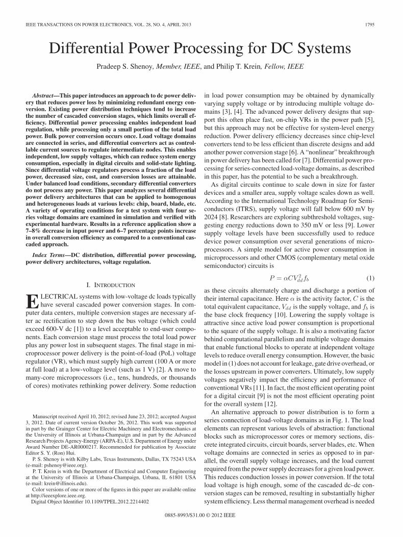
Fundamentally, a controllable current source can regulate thelocal voltage at the node between adjacent series loads. Thecurrent source provides the difference between adjacent loadcurrents, as seen in Fig. 3(a). The steady-state current providedby the ith local voltage regulator is
IVR ,i = Iload,i − Iload,i+1 (2)
where Iload,i is the current of the ith load. If the steady-statecurrents of two adjacent loads match, no current needs to beprovided by the differential VR. If there is a mismatch, thedifferential VR provides only the difference in current. This is atremendous potential benefit because under reasonably matchedoperating conditions, the differential VRs process only a fractionof the total load power. Bulk power comes from a single-powersupply at the relatively high total series voltage. Differentialconverters can also act to bypass current as needed to maintaina well regulated local voltage, as shown in Fig. 3(b).
Many converter topologies can function as differential VRs,motivated in part by circuits developed for battery balancingin series strings [30], [31]. The converters can be on-chip oroff-chip, isolated or nonisolated, inductive, or capacitive. Forsimplicity and flexibility, this research begins with a buck–boost
1798 IEEE TRANSACTIONS ON POWER ELECTRONICS, VOL. 28, NO. 4, APRIL 2013
Fig. 3. Differential power converters act as controllable current sources toregulate intermediate voltage nodes.
switching configuration similar to [30]. The main focus is onthe overall regulation architecture rather than the local convertertopology or implementation. It is useful to notice that if thereare n load elements, only n–1 differential VRs are needed toprovide complete voltage control, as depicted in Fig. 3(a). Thetop voltage domain is regulated by the main power supply (i.e., itis the nth control actuator). If n differential VRs are employed,as shown in Fig. 3(b), the control system has an extra degree offreedom. This can be used, for example, to minimize the currentthat is processed. The following subsections examine severallocal series power delivery architectures.
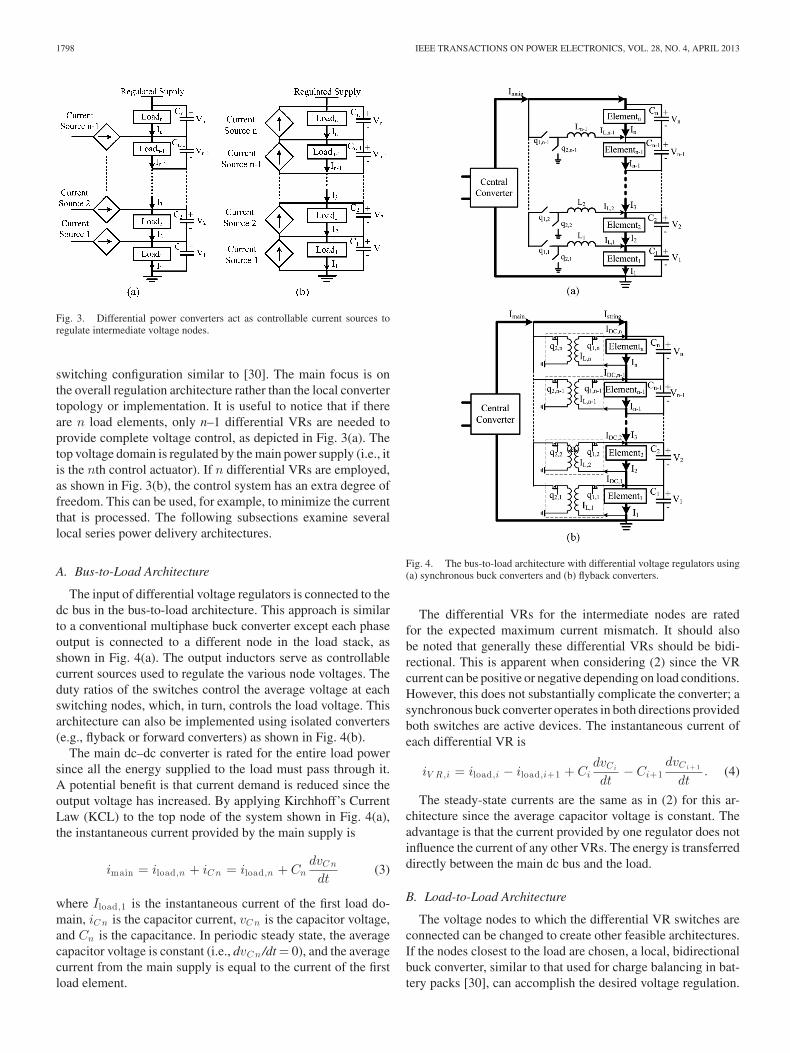
A. Bus-to-Load Architecture
The input of differential voltage regulators is connected to thedc bus in the bus-to-load architecture. This approach is similarto a conventional multiphase buck converter except each phaseoutput is connected to a different node in the load stack, asshown in Fig. 4(a). The output inductors serve as controllablecurrent sources used to regulate the various node voltages. Theduty ratios of the switches control the average voltage at eachswitching nodes, which, in turn, controls the load voltage. Thisarchitecture can also be implemented using isolated converters(e.g., flyback or forward converters) as shown in Fig. 4(b).
The main dc–dc converter is rated for the entire load powersince all the energy supplied to the load must pass through it.A potential benefit is that current demand is reduced since theoutput voltage has increased. By applying Kirchhoff’s CurrentLaw (KCL) to the top node of the system shown in Fig. 4(a),the instantaneous current provided by the main supply is
imain = iload,n + iC n = iload,n + CndvC n
dt(3)
where Iload,1 is the instantaneous current of the first load do-main, iC n is the capacitor current, vC n is the capacitor voltage,and Cn is the capacitance. In periodic steady state, the averagecapacitor voltage is constant (i.e., dvC n /dt = 0), and the averagecurrent from the main supply is equal to the current of the firstload element.
Fig. 4. The bus-to-load architecture with differential voltage regulators using(a) synchronous buck converters and (b) flyback converters.
The differential VRs for the intermediate nodes are ratedfor the expected maximum current mismatch. It should alsobe noted that generally these differential VRs should be bidi-rectional. This is apparent when considering (2) since the VRcurrent can be positive or negative depending on load conditions.However, this does not substantially complicate the converter; asynchronous buck converter operates in both directions providedboth switches are active devices. The instantaneous current ofeach differential VR is
iV R,i = iload,i − iload,i+1 + CidvCi
dt− Ci+1
dvCi + 1
dt. (4)
The steady-state currents are the same as in (2) for this ar-chitecture since the average capacitor voltage is constant. Theadvantage is that the current provided by one regulator does notinfluence the current of any other VRs. The energy is transferreddirectly between the main dc bus and the load.
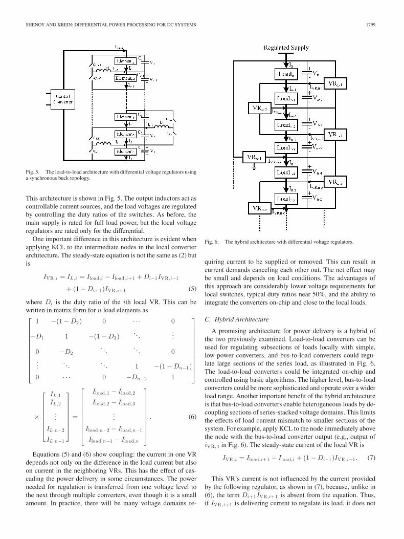
B. Load-to-Load Architecture
The voltage nodes to which the differential VR switches areconnected can be changed to create other feasible architectures.If the nodes closest to the load are chosen, a local, bidirectionalbuck converter, similar to that used for charge balancing in bat-tery packs [30], can accomplish the desired voltage regulation.
SHENOY AND KREIN: DIFFERENTIAL POWER PROCESSING FOR DC SYSTEMS 1799
Fig. 5. The load-to-load architecture with differential voltage regulators usinga synchronous buck topology.
This architecture is shown in Fig. 5. The output inductors act ascontrollable current sources, and the load voltages are regulatedby controlling the duty ratios of the switches. As before, themain supply is rated for full load power, but the local voltageregulators are rated only for the differential.
One important difference in this architecture is evident whenapplying KCL to the intermediate nodes in the local converterarchitecture. The steady-state equation is not the same as (2) butis
where Di is the duty ratio of the ith local VR. This can bewritten in matrix form for n load elements as⎡⎢⎢⎢⎢⎢⎢⎢⎢⎢⎢⎣
1 −(1 − D2) 0 · · · 0
−D1 1 −(1 − D3). . .
...
0 −D2. . .
. . . 0...
. . .. . . 1 −(1 − Dn−1)
0 · · · 0 −Dn−2 1
⎤⎥⎥⎥⎥⎥⎥⎥⎥⎥⎥⎦
×
⎡⎢⎢⎢⎢⎢⎢⎣
IL,1IL,2
...
IL,n−2
IL,n−1
⎤⎥⎥⎥⎥⎥⎥⎦
=
⎡⎢⎢⎢⎢⎢⎢⎢⎢⎣
Iload,1 − Iload,2
Iload,2 − Iload,3
...
Iload,n−2 − Iload,n−1
Iload,n−1 − Iload,n
⎤⎥⎥⎥⎥⎥⎥⎥⎥⎦
. (6)
Equations (5) and (6) show coupling: the current in one VRdepends not only on the difference in the load current but alsoon current in the neighboring VRs. This has the effect of cas-cading the power delivery in some circumstances. The powerneeded for regulation is transferred from one voltage level tothe next through multiple converters, even though it is a smallamount. In practice, there will be many voltage domains re-
Fig. 6. The hybrid architecture with differential voltage regulators.
quiring current to be supplied or removed. This can result incurrent demands canceling each other out. The net effect maybe small and depends on load conditions. The advantages ofthis approach are considerably lower voltage requirements forlocal switches, typical duty ratios near 50%, and the ability tointegrate the converters on-chip and close to the local loads.
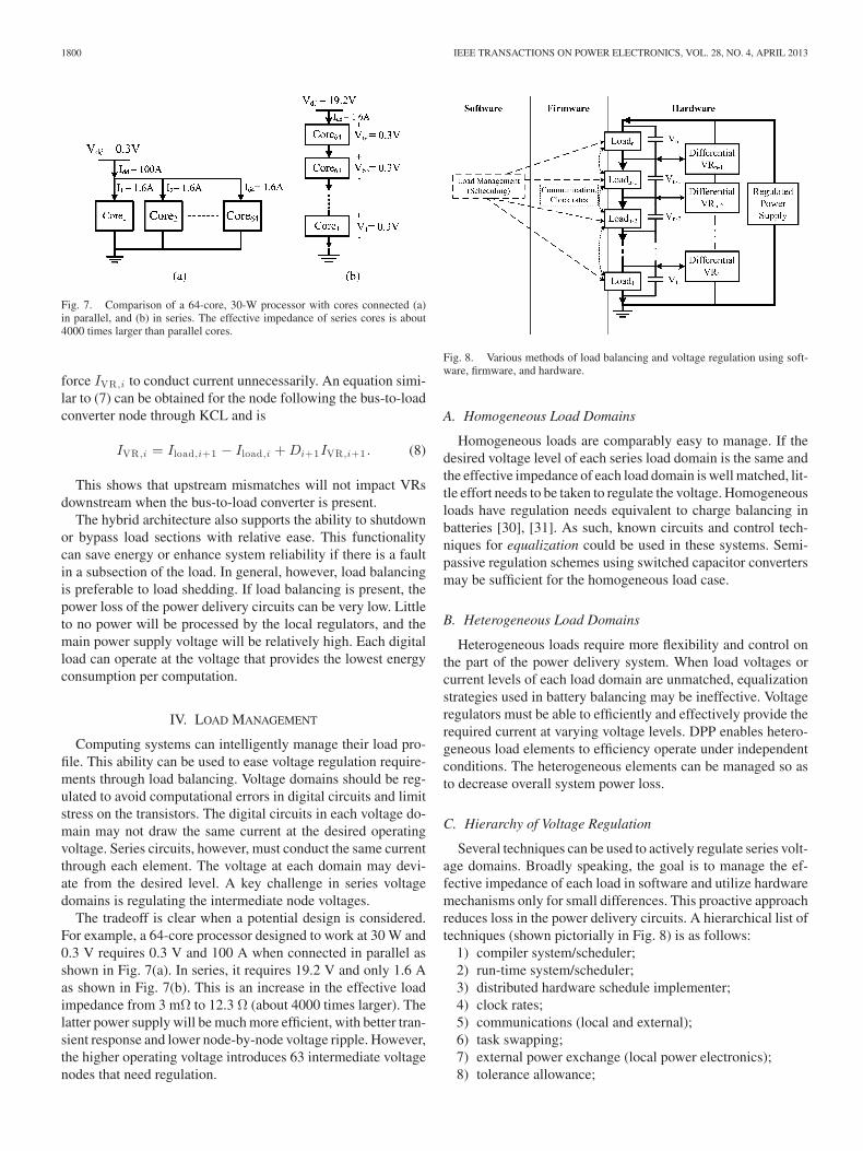
C. Hybrid Architecture
A promising architecture for power delivery is a hybrid ofthe two previously examined. Load-to-load converters can beused for regulating subsections of loads locally with simple,low-power converters, and bus-to-load converters could regu-late large sections of the series load, as illustrated in Fig. 6.The load-to-load converters could be integrated on-chip andcontrolled using basic algorithms. The higher level, bus-to-loadconverters could be more sophisticated and operate over a widerload range. Another important benefit of the hybrid architectureis that bus-to-load converters enable heterogeneous loads by de-coupling sections of series-stacked voltage domains. This limitsthe effects of load current mismatch to smaller sections of thesystem. For example, apply KCL to the node immediately abovethe node with the bus-to-load converter output (e.g., output ofiVR ,3 in Fig. 6). The steady-state current of the local VR is
This VR’s current is not influenced by the current providedby the following regulator, as shown in (7), because, unlike in(6), the term Di+1IVR ,i+1 is absent from the equation. Thus,if IVR ,i+1 is delivering current to regulate its load, it does not
1800 IEEE TRANSACTIONS ON POWER ELECTRONICS, VOL. 28, NO. 4, APRIL 2013
Fig. 7. Comparison of a 64-core, 30-W processor with cores connected (a)in parallel, and (b) in series. The effective impedance of series cores is about4000 times larger than parallel cores.
force IVR ,i to conduct current unnecessarily. An equation simi-lar to (7) can be obtained for the node following the bus-to-loadconverter node through KCL and is
IVR ,i = Iload,i+1 − Iload,i + Di+1IVR ,i+1 . (8)
This shows that upstream mismatches will not impact VRsdownstream when the bus-to-load converter is present.
The hybrid architecture also supports the ability to shutdownor bypass load sections with relative ease. This functionalitycan save energy or enhance system reliability if there is a faultin a subsection of the load. In general, however, load balancingis preferable to load shedding. If load balancing is present, thepower loss of the power delivery circuits can be very low. Littleto no power will be processed by the local regulators, and themain power supply voltage will be relatively high. Each digitalload can operate at the voltage that provides the lowest energyconsumption per computation.
IV. LOAD MANAGEMENT
Computing systems can intelligently manage their load pro-file. This ability can be used to ease voltage regulation require-ments through load balancing. Voltage domains should be reg-ulated to avoid computational errors in digital circuits and limitstress on the transistors. The digital circuits in each voltage do-main may not draw the same current at the desired operatingvoltage. Series circuits, however, must conduct the same currentthrough each element. The voltage at each domain may devi-ate from the desired level. A key challenge in series voltagedomains is regulating the intermediate node voltages.
The tradeoff is clear when a potential design is considered.For example, a 64-core processor designed to work at 30 W and0.3 V requires 0.3 V and 100 A when connected in parallel asshown in Fig. 7(a). In series, it requires 19.2 V and only 1.6 Aas shown in Fig. 7(b). This is an increase in the effective loadimpedance from 3 mΩ to 12.3 Ω (about 4000 times larger). Thelatter power supply will be much more efficient, with better tran-sient response and lower node-by-node voltage ripple. However,the higher operating voltage introduces 63 intermediate voltagenodes that need regulation.
Fig. 8. Various methods of load balancing and voltage regulation using soft-ware, firmware, and hardware.
A. Homogeneous Load Domains
Homogeneous loads are comparably easy to manage. If thedesired voltage level of each series load domain is the same andthe effective impedance of each load domain is well matched, lit-tle effort needs to be taken to regulate the voltage. Homogeneousloads have regulation needs equivalent to charge balancing inbatteries [30], [31]. As such, known circuits and control tech-niques for equalization could be used in these systems. Semi-passive regulation schemes using switched capacitor convertersmay be sufficient for the homogeneous load case.
B. Heterogeneous Load Domains
Heterogeneous loads require more flexibility and control onthe part of the power delivery system. When load voltages orcurrent levels of each load domain are unmatched, equalizationstrategies used in battery balancing may be ineffective. Voltageregulators must be able to efficiently and effectively provide therequired current at varying voltage levels. DPP enables hetero-geneous load elements to efficiency operate under independentconditions. The heterogeneous elements can be managed so asto decrease overall system power loss.
C. Hierarchy of Voltage Regulation
Several techniques can be used to actively regulate series volt-age domains. Broadly speaking, the goal is to manage the ef-fective impedance of each load in software and utilize hardwaremechanisms only for small differences. This proactive approachreduces loss in the power delivery circuits. A hierarchical list oftechniques (shown pictorially in Fig. 8) is as follows:
1) compiler system/scheduler;2) run-time system/scheduler;3) distributed hardware schedule implementer;4) clock rates;5) communications (local and external);6) task swapping;7) external power exchange (local power electronics);8) tolerance allowance;
SHENOY AND KREIN: DIFFERENTIAL POWER PROCESSING FOR DC SYSTEMS 1801
9) global supply;10) protection;
The first lines of defense in voltage regulation occur at thesoftware level. If the desired voltage of each voltage domain isequal, the operating system should manage software threads atcompile time or run time to evenly balance the computationalload of each element. The operating system can also dispatchactivity unevenly if unequal voltage levels are desired. On com-puter servers, virtual machines could be managed so that thecomputational activity on each motherboard or server blade isapproximately equal.
Another regulation layer is at the firmware level. A task man-ager can distribute operations among computational elementswithout intervention from the operating system. Task swappingand task rotation are possible techniques. Clock rates can beadjusted to throttle the activity within each voltage domain andcontrol the effective load impedance. It is important to keep inmind that, even though Fig. 8 abstractly displays one circuitat each voltage level, a voltage domain could support severalelements in parallel. The activity of all the elements must bemanaged to control the effective load impedance.
If the preceding methods are unable to maintain voltages atthe specified targets, hardware-based regulation approaches canbe used. This includes using local dc–dc converters to activelyregulate the voltage [32] as discussed in Section III. The uniqueadvantage of DPP is that power delivery circuits process onlya fraction of the load power when providing the difference incurrent between load domains. The voltage overshoot or under-shoot caused by load transients will also be less severe sinceload transient magnitude will be substantially reduced (e.g., bya factor of 1/n, where n is the number of voltage domains). Inextreme situations, Zener diodes can protect local domains fromovervoltage conditions.
D. Communication Overhead
While series-connected voltage domains have considerablepromise, level shifting for interdomain communications com-plicates implementation. Level conversion is standard in mod-ern digital circuits, and microprocessors which employ multi-ple voltage domains already exist. Other viable communicationtechniques include capacitively driven wires [33], optical inter-connects [34], and even wireless transmission [35]. It remainsto be seen whether or not communication overhead would in-crease. These issues motivate computer architectures that reducecommunications or limit it so that latency and power overheadhave minimal impact—a typical architectural issue in parallelcomputing. Similarly, the series configuration may lend itselfto applications in which there is little interdependence in thedata, and computations can be made in parallel without signifi-cant interaction. The goal may be to develop an initial mappingthat balances workloads across computational units with limitedcommunication.
V. ENERGY CONSUMPTION ANALYSIS
A comparative analysis of a candidate system is undertaken toquantify the benefits of the DPP approach. As digital circuits are
a motivating factor, system efficiency for a multicore micropro-cessor with separate voltage domains for each core is examined.While the emerging approach is to have an additional cascadedVR to supply an independent voltage for each core, DPP canmeet the same objectives with less energy consumption.
A. Independent Loads With Cascaded VRs
An additional conversion stage is needed if independent volt-age levels are desired in a conventional power delivery architec-ture. Each PoL converter must be rated for the full-load powerof its respective load element and must process all the powerdelivered to the load. This added conversion stage decreasesoverall power conversion efficiency. It is also difficult to designand implement an integrated conversion circuit that is efficientover a wide load range. While peak efficiency numbers are oftenquoted for dc–dc converters, the important figure of merit is con-verter energy efficiency based on an extended interval of typicaloperation. This is defined as η = Eout /Ein , where Eout is thetotal energy output for the entire duration of a suitable test andEin is the total input energy. In typical computing applications,the system operates at light or medium load levels much of thetime. This means overall efficiency is load-profile dependent,and is a weighted average of power conversion efficiency.
Another figure of merit is the total system input energy Ein .In the end, energy is paid for whether it is shown on a utility billfor a data center or as battery life in a portable application. Forcomparison, let us consider the dc portion of a typical computerserver. There will likely be an isolated dc–dc converter and avoltage regulator upstream from the microprocessor load. Theinput energy is
Ein =Eload
η1η2(9)
where Eload is the energy consumed in the microprocessor, η1 isthe efficiency of the isolated dc–dc converter, and η2 is the board-level VR efficiency. If independent voltage domains are desiredto reduce load-energy consumption, a cascaded conversion stageis necessary and the input energy becomes
Ein =E ′
load
η1η2η3(10)
where E′load is the reduced energy consumed by the load and η3
is the efficiency of the added conversion stage. For this approachto be worthwhile, the input energy should be lower than theprevious case (i.e., (10) is less than (9)). Thus, the following issought
E ′load < η3Eload . (11)
The reduction in energy consumption must compensate forthe energy lost in the extra conversion stage. This assumes theefficiency of the other energy conversion stages (i.e., η1 and η2)remains the same. Even if the energy consumed by the load isreduced sufficiently, the overall gains in terms of input energyreduction are diminished by the added conversion loss. Anotherperspective can be taken by rearranging (11) to conclude thatthe required efficiency of the additional conversion stage needs
1802 IEEE TRANSACTIONS ON POWER ELECTRONICS, VOL. 28, NO. 4, APRIL 2013
to be sufficiently high. The efficiency should be
η3 >E ′
load
Eload(12)
to ensure input energy savings for the system.
B. Independent Loads With Differential VRs
An advantage of series-connected voltage domains is thatthe each domain voltage is intrinsically independent. Althoughdifferential VRs generally are still needed for regulation, theyprocess only a fraction of the total load power. Cascaded con-version stages can be eliminated if the overall voltage of theseries domains is sufficiently high. Consider the same system asabove using differential VRs instead of cascaded converters toprovide independent voltage domains for multiprocessor cores.The input energy to the system is
Ein =Eload + EDVRloss
η1η2(13)
where EDVRloss is the energy loss due to differential powerprocessing, η1 is the efficiency of the isolated dc–dc converter,and η2 is the efficiency of the second conversion stage. Thefraction of the load energy processed by differential VRs canbe represented as an energy-processing factor β, where β =EDVR/ELoad . Thus, the energy lost in differential VRs is
EDVRloss =βEload(1 − η4)
η4(14)
where η4 is the efficiency of the differential VRs. Equation (13)can then be explicitly written as
Ein =Eload
η1η2+
βEload(1 − η4)η1η2η4
= Eload
(η4 + β(1 − η4)
η1η2η4
).
(15)If the voltage of the series load stack is high enough to remove
the second conversion stage, η2 is effectively equal to 1.
C. Comparison
The goal now is to determine under what conditions the dif-ferential power processing system results in lower energy con-sumption than the conventional system with cascaded VRs. Us-ing (10) and (15), if the differential VR system consumes lessenergy, the following must be true:
Eload
(η4 + β(1 − η4)
η1η2η4
)<
Eload
η1η2η3. (16)
Assuming the energy consumed in the load and the upstreamconversion efficiency is the same in both systems, this expres-sion can be simplified to
η4 + β(1 − η4)η4
<1η3
. (17)
Hence, the fraction of load energy that can be processed bydifferential converters and result in less total energy consump-tion is
β <
(1 − η3
η3
)(η4
1 − η4
). (18)
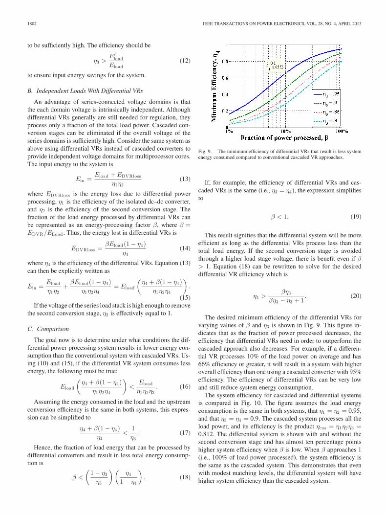
Fig. 9. The minimum efficiency of differential VRs that result is less systemenergy consumed compared to conventional cascaded VR approaches.
If, for example, the efficiency of differential VRs and cas-caded VRs is the same (i.e., η3 = η4), the expression simplifiesto
β < 1. (19)
This result signifies that the differential system will be moreefficient as long as the differential VRs process less than thetotal load energy. If the second conversion stage is avoidedthrough a higher load stage voltage, there is benefit even if β> 1. Equation (18) can be rewritten to solve for the desireddifferential VR efficiency which is
η4 >βη3
βη3 − η3 + 1. (20)
The desired minimum efficiency of the differential VRs forvarying values of β and η3 is shown in Fig. 9. This figure in-dicates that as the fraction of power processed decreases, theefficiency that differential VRs need in order to outperform thecascaded approach also decreases. For example, if a differen-tial VR processes 10% of the load power on average and has66% efficiency or greater, it will result in a system with higheroverall efficiency than one using a cascaded converter with 95%efficiency. The efficiency of differential VRs can be very lowand still reduce system energy consumption.
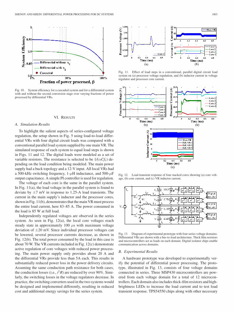
The system efficiency for cascaded and differential systemsis compared in Fig. 10. The figure assumes the load energyconsumption is the same in both systems, that η1 = η2 = 0.95,and that η3 = η4 = 0.9. The cascaded system processes all theload power, and its efficiency is the product ηcas = η1η2η3 =0.812. The differential system is shown with and without thesecond conversion stage and has almost ten percentage pointshigher system efficiency when β is low. When β approaches 1(i.e., 100% of load power processed), the system efficiency isthe same as the cascaded system. This demonstrates that evenwith modest matching levels, the differential system will havehigher system efficiency than the cascaded system.
SHENOY AND KREIN: DIFFERENTIAL POWER PROCESSING FOR DC SYSTEMS 1803
Fig. 10. System efficiency for a cascaded system and for a differential systemwith and without the second conversion stage over varying fractions of powerprocessed by differential VRs.
VI. RESULTS
A. Simulation Results
To highlight the salient aspects of series-configured voltageregulation, the setup shown in Fig. 5 using load-to-load differ-ential VRs with four digital circuit loads was compared with aconventional parallel load system supplied by one main VR. Thesimulated response of each system to equal load steps is shownin Figs. 11 and 12. The digital loads were modeled as a set ofvariable resistors. The resistance is selected to be 1/(αCfb ) de-pending on the load condition being modeled. The main powersupply had a buck topology and a 12-V input. All local VRs hada 500-kHz switching frequency, 1-μH inductance, and 500-μFoutput capacitance. A simple PI controller is used for regulation.
The voltage of each core is the same in the parallel system.In Fig. 11(a), the load voltage in the parallel system is found todeviate by ±7 mV in response to 1.25-A load transients. Thecurrent in the main supply’s inductor and the processor cores,shown in Fig. 11(b), demonstrates that the main VR must processthe entire load current, here 83–85 A. The power consumed inthe load is 85 W at full load.
Independently regulated voltages are observed in the seriessystem. As seen in Fig. 12(a), the local core voltages reachsteady state in approximately 100 μs with maximum voltagedeviation of ±20 mV. Since individual processor voltages canbe lowered, several processor currents decrease, as shown inFig. 12(b). The total power consumed by the load in this case isabout 70 W. The VR currents included in Fig. 12(c) demonstrateactive regulation of core voltages with reduced power process-ing. The main power supply only provides about 20 A andthe differential VRs provide less than 5A each. This results insubstantially reduced power loss in the power delivery circuits.Assuming the same conduction path resistance for both cases,the conduction losses (i.e., i2R) are reduced by over 90%. Simi-larly, the switching losses in the voltage regulators decrease. Inpractice, the switching converters used in the two systems wouldbe designed and implemented differently, resulting in reducedcost and additional energy savings for the series system.
Fig. 11. Effect of load steps in a conventional, parallel digital circuit loadsystem on (a) processor voltage regulation, and (b) inductor current in voltageregulator and processor core current.
Fig. 12. Load-transient response of four stacked cores showing (a) core volt-age, (b) core current, and (c) VR inductor current.
Fig. 13. Diagram of experimental prototype with four series voltage domains.Differential VRs are shown with a bus-to-load architecture. Thick film resistorsand microcontrollers act as loads on each domain. Digital isolator chips enablecommunication across domains.
B. Experimental Results
A hardware prototype was developed to experimentally ver-ify the potential of differential power processing. The proto-type, illustrated in Fig. 13, consists of four voltage domainsconnected in series. Three MSP430 microcontrollers are pow-ered from each voltage domain for a total of 12 microcon-trollers. Each domain also includes thick-film resistors and high-brightness LEDs to increase the load current and to test loadtransient response. TPS54550 chips along with other necessary
1804 IEEE TRANSACTIONS ON POWER ELECTRONICS, VOL. 28, NO. 4, APRIL 2013
TABLE ICOMPARISON OF CASCADED AND DIFFERENTIAL ARCHITECTURE CONVERSION EFFICIENCY
components were selected for voltage regulation of the threeintermediate nodes. A central converter regulated the over-all voltage. Microcontrollers communicated across voltagedomains using the SPI protocol through ISO7241C digitalisolators.
Several load conditions were examined to compare the effi-ciency of differential power delivery with the traditional cas-caded approach. The measured results are tabulated in Table I.The cascaded architecture was formed by reconfiguring thehardware prototype, and the same voltage regulation circuitswere used. Voltage domains 1 through 4 were regulated at 2.25 V,2.75 V, 2.5 V, and 2.5 V, respectively. For load cases 1 and 2,the load was varied on the second domain V2 , and for cases 3and 4 the first domain load was adjusted. As seen in Table I,the differential architecture can regulate the same loads withabout 1-W less input power. This represents a 7–8% decrease ininput power and an increase in overall conversion efficiency byabout 6–7 percentage points. This improvement is due to boththe central converter efficiency increasing from around 91% to93% and the VRs effective efficiency increasing from about92% to 97%. Power loss in energy conversion circuits decreasesby 40–50%.
The prototype system was tested with load steps on the lowestvoltage domain using a buck–boost bus-to-load architecture.Fig. 14(a) shows the current into each regulated node. The mainpower supply current Iin increases as the load increases. Theaverage current of the differential VRs that regulate two higherintermediate voltage nodes (i.e., IL2 and IL3) does not change.Only the differential VR for the lowest voltage domain respondsto the load increase by increasing its current IL1 . This is inline with the analysis of the bus-to-load architecture. Fig. 14(b)shows the differential voltage of the second domain V2 , thevoltage with respect to ground of domains one (V1) and two(V21), and the differential VR current for domain one (IL1).The voltage of domain one (V1) dips during a load increase andovershoots during a load decrease as expected. Although thevoltage of the second domain with respect to ground also dipsduring the transient, its differential voltage increases during theload step up.
The system was also tested with a load transient on the sec-ond voltage domain. Fig. 15 shows the response of bus-to-loaddifferential VRs. The current supplied by the second differ-ential VR (IL2) increases to meet the increased load demandon that domain. The differential VR for domain one removesthis current (i.e., (IL1) is negative) in order to regulate domainone (V1). The input current (Iin ) increases since the overallload has increased. These results validate the analysis presentedpreviously.
Fig. 14. Response to a load step on domain one of four series voltage domains.In (a), the main supply current and differential VR currents are shown. In (b),the differential voltage of domain two, the voltage with respect to ground ofdomain one and two, and the current in the differential VR are shown.
Fig. 15. Response to a load step on domain two of four series voltage domains.The gate-to-source voltage Vgs of the load switch indicates the timing of thetransient. The main supply input current and differential VR currents are alsoshown.
SHENOY AND KREIN: DIFFERENTIAL POWER PROCESSING FOR DC SYSTEMS 1805
VII. OTHER APPLICATIONS
Thus far the discussion surrounding DPP has focused ondigital loads. Other homogeneous and heterogeneous elementsacting as loads, sources, and energy storage devices can benefitfrom this approach as well. Some systems with intrinsicallyheterogeneous characteristics such as solar photovolatics (PV)and solid-state lighting are well suited to DPP. To demonstratethe generality, these two applications are examined further.
A. Solid-State Lighting
LEDs are increasingly being used in lighting applications.LED characteristics can vary substantially, and a binning pro-cess is commonly employed by manufacturers. Furthermore,some applications like RGB (red, green, and blue) lighting re-quire dissimilar LEDs whose voltage and current characteristicsdo not match. Linear current regulators used to overcome thisdrawback add cost and decrease efficiency. The DPP conceptcan be applied to enable sections of a series string of LEDsto operate at independent voltage and current levels with lesspower-processing overhead than conventional solutions.
B. Solar Photovoltaics
Maximum power point (MPP) current mismatch is a well-known challenge in series solar photovoltaic (PV) systems.Module-integrated converters are sometimes employed to over-come MPP mismatch. The trouble is that the energy loss fromthe added conversion stage can outweigh the increase in energygenerated by the PV system. DPP has been successfully appliedto series PV panels in [36]–[38]. Some earlier studies take asimilar approach [39], [40]. A high level of MPP granularity isachieved, and only a small fraction of total power is processedby differential converters. Another benefit is increased systemreliability.
VIII. CONCLUSION
System-level design of digital circuits must change to ad-dress power concerns. Currently available options will not besufficient to overcome the “power wall.” Series-connected loadvoltage domains can reduce power consumption in the loadand energy loss in the power delivery system. This paper intro-duces and analyzes differential power processing architecturesto facilitate series-connected circuits and is in stark contrast toconventional methods that add energy conversion stages to meetpower delivery objectives. A major benefit of differential powerprocessing is that local voltage regulators process only a frac-tion of the load power when a load current mismatch exists. Thisimproves performance, significantly reduces power loss, lowerscosts, and reduces component size. Converter components withlower ratings can be used, allowing integrated converters withsimple controls.
In digital applications, this approach is enabled by computa-tional load management and regulation of the intermediate-nodevoltages. A variety of regulation mechanisms ranging from soft-ware to power electronics is feasible. A series connection facil-itates substantial voltage reduction. Independent supply voltage
levels for heterogeneous loads can be varied dynamically tooperate each load at its most efficient operating point. Thistechnique is especially suited for multicore processors that runmost efficiently at very low voltage (e.g., 0.3 V). In turn, thenumber of pins dedicated to power is reduced.
Analysis has shown that differential power processing willresult in a more efficient system than conventional approaches.Three different differential power delivery architectures werepresented and compared. Simulation and experimental resultsfor a test system with four series voltage domains demonstrateits validity. A 7–8% reduction in input power and an increasein overall conversion efficiency by 6–7 percentage points com-pared to the conventional cascaded approach were measured forseveral load conditions. This represents a 40%–50% decreasein power loss in energy conversion circuits. Differential powerprocessing can be successfully applied to integrated circuits,solid-state lighting, solar photovolatics, and other low-voltagedc power delivery applications.
ACKNOWLEDGMENT
The authors would like to thank T. Neyens and I. Federovfor assisting in prototype hardware builds. The authors wouldalso like to thank N.R. Shanbhag, R. Campbell, R. Abdallah, S.Zhang, and H. Kharbanda for insights related to CMOS circuitsand software management.
The information, data, or work presented herein was fundedin part by an agency of the United States Government. Neitherthe United States Government nor any agency thereof, nor anyof their employees, makes any warranty, express or implied,or assumes any legal liability or responsibility for the accuracy,completeness, or usefulness of any information, apparatus, prod-uct, or process disclosed, or represents that its use would notinfringe privately owned rights. Reference herein to any specificcommercial product, process, or service by trade name, trade-mark, manufacturer, or otherwise does not necessarily constituteor imply its endorsement, recommendation, or favoring by theUnited States Government or any agency thereof. The views andopinions of authors expressed herein do not necessarily state orreflect those of the United States Government or any agencythereof.
REFERENCES
[1] P. T. Krein, “A discussion of data center power challenges across thesystem,” in Proc. IEEE Int. Conf. Energy Aware Comput., Dec. 2010.
[2] Intel Corp., “Voltage regulator module (VRM) and enter-prise voltage regulator-down (EVRD) 11.1 design guidelines,”www.intel.com/assets/PDF/designguide/321736.pdf, Tech. Rep., 321736,Sep. 2009.
[3] M. Nakai et al., “Dynamic voltage and frequency management for a low-power embedded microprocessor,” IEEE J. Solid-State Circuits, vol. 40,no. 1, pp. 28–35, Jan. 2005.
[4] D. E. Lackey et al., “Managing power and performance for system-on-chipdesigns using voltage islands,” in Proc. ACM/IEEE Int. Conf. ComputerAided Design, Nov. 2002, pp. 195–202.
[5] W. Kim, D. Brooks, and G.-Y. Wei, “A fully-integrated 3-level DC-DCconverter for nanosecond-scale DVFS,” IEEE J. Solid-State Circuits,vol. 47, no. 1, pp. 206–219, Jan. 2012.
[6] H. P. Le, M. Seeman, S. R. Sanders, V. Sathe, S. Naffziger, and E. Alon,“A 32 nm fully integrated reconfigurable switched-capacitor DC-DC con-verter delivering 0.55 W/mm2 at 81% efficiency,” in Proc. IEEE Int.Solid-State Circuits Conf., Feb. 2010, pp. 210–211.
1806 IEEE TRANSACTIONS ON POWER ELECTRONICS, VOL. 28, NO. 4, APRIL 2013
[7] S. L. Smith, “Power optimization in the connected world,” presented atthe IEEE Int. Conf. Energy Aware Comput., Cairo, Egypt, Dec. 2010.
[9] B. H. Calhoun, A. Wang, and A. Chandrakasan, “Modeling and sizing forminimum energy operation in subthreshold circuits,” IEEE J. Solid-StateCircuits, vol. 40, no. 9, pp. 1778–1786, Sep. 2005.
[10] S. Borkar, “Design challenges of technology scaling,” IEEE Micro,vol. 19, no. 4, pp. 23–29, Jul./Aug. 1999.
[11] P. S. Shenoy, V. T. Buyukdegirmenci, A. M. Bazzi, and P. T. Krein, “Systemlevel trade-offs of microprocessor supply voltage reduction,” presented atthe Proc. IEEE Int. Conf. Energy Aware Comput., Cairo, Egypt, 2010.
[12] R. A. Abdallah, P. S. Shenoy, N. R. Shanbhag, and P. T. Krein, “Systemenergy minimization via joint optimization of the DC-DC converter andthe core,” in Proc. IEEE Int. Symp. Low Power Electron. Design, Aug.2011, pp. 97–102.
[13] J. Dean and S. Ghemawat, “MapReduce: Simplified data processing onlarge clusters,” Commun. ACM, vol. 51, no. 1, pp. 107–113, Jan. 2008.
[14] S. Rajapandian, X. Zheng, and K. L. Shepard, “Implicit DC-DC downcon-version through charge-recycling,” IEEE J. Solid-State Circuits, vol. 40,no. 4, pp. 846–852, Apr. 2005.
[15] S. Rajapandian, K. L. Shepard, P. Hazucha, and T. Karnik, “High-voltagepower delivery through charge recycling,” IEEE J. Solid-State Circuits,vol. 41, no. 6, pp. 1400–1410, Jun. 2006.
[16] G. Jie and C. H. Kim, “Multi-story power delivery for supply noise re-duction and low voltage operation,” in Proc. IEEE Int. Symp. Low PowerElectron. Design, Aug. 2005, pp. 192–197.
[17] P. Jain, T. H. Kim, J. Keane, and C. H. Kim, “A multi-story power deliverytechnique for 3D integrated circuits,” in Proc. IEEE Int. Symp. Low PowerElectron. Design, Aug. 2008, pp. 57–62.
[18] A. C. Cabe, Z. Qi, and M. R. Stan, “Stacking SRAM banks for ultra lowpower standby mode operation,” in Proc. ACM/IEEE Design Automat.Conf., Jun. 2010, pp. 699–704.
[19] P. P. Gelsinger, “Microprocessors for the new millennium: Challenges,opportunities, and new frontiers,” in Proc. IEEE Int. Solid-State CircuitsConf., 2001, pp. 22–25.
[20] T. Kuroda, “Low-power, high-speed CMOS VLSI design,” in Proc. IEEEInt. Conf. Comput. Design: VLSI Comput. Processors, 2002, pp. 310–315.
[21] M. P. Sayani and J. Wanes, “Analyzing and determining optimum on-board power architectures for 48 V-input systems,” in Proc. IEEE AppliedPower Electron. Conf., Feb. 2003, pp. 781–785.
[22] L. Brush, “Distributed power architecture demand characteristics,” inProc. IEEE Applied Power Electron. Conf., 2004, pp. 342–345.
[23] P. Miquel and F. Gourvil, “Distributed power architecture in the contextof the cost effective data center,” in Proc. IEEE Int. Telecommun. EnergyConf., 2002, pp. 427–431.
[24] P. Lindman and L. Thorsell, “Applying distributed power modules intelecom systems,” IEEE Trans. Power Electron., vol. 11, no. 2, pp. 365–373, Mar. 1996.
[25] B. Narveson, “How many isolated dc-dc’s do you really need?” in Proc.IEEE Applied Power Electron. Conf., Mar. 1996, pp. 692–695.
[26] R. V. White, “Emerging on-board power architectures,” in Proc. IEEEApplied Power Electron. Conf., Feb. 2003, pp. 799–804.
[27] E. Lam, R. Bell, and D. Ashley, “Revolutionary advances in distributedpower systems,” in Proc. IEEE Applied Power Electron. Conf., Feb. 2003,pp. 30–36.
[28] B. C. Narveson, “What is the right bus voltage?,” in Proc. IEEE AppliedPower Electron. Conf., Feb. 1998, pp. 883–888.
[29] Y. C. Ren, M. Xu, K. Yao, Y. Meng, and F. C. Lee, “Two-stage approach for12-V VR,” IEEE Trans. Power Electron., vol. 19, no. 6, pp. 1498–1506,Nov. 2004.
[30] G. L. Brainard, “Non-dissipative battery charger equalizer,” U.S. Patent5479083, Dec. 26, 1995.
[31] C. Pascual, P. T. Krein, “Switched capacitor system for automatic batteryequalization,” U.S. Patent 5710504, Jan. 20, 1998.
[32] P. S. Shenoy, I. Fedorov, T. Neyens, and P. T. Krein, “Power delivery forseries connected voltage domains in digital circuits,” in Proc. IEEE Int.Conf. Energy Aware Comput., Nov./Dec. 2011.
[33] R. Ho et al., “High-speed and low-energy capacitively-driven on-chipwires,” in Proc. IEEE Int. Solid-State Circuits Conf., Feb. 2007, pp. 412–612.
[34] M. Haurylau et al., “On-chip optical interconnect roadmap: Challengesand critical directions,” IEEE J. Sel. Topics Quantum Electron., vol. 12,no. 6, pp. 1699–1705, Nov./Dec. 2006.
[35] C. Hu, R. Khanna, J. Nejedlo, K. Hu, H. Liu, and P. Y. Chiang, “A 90 nm-CMOS, 500 Mbps, 3–5 GHz fully-integrated IR-UWB transceiver with
multipath equalization using pulse injection-locking for receiver phasesynchronization,” IEEE J. Solid-State Circuits, vol. 46, no. 5, pp. 1076–1088, May 2011.
[36] P. S. Shenoy, B. Johnson, and P. T. Krein, “Differential power process-ing architecture for increased energy production and reliability of photo-voltaic systems,” in Proc. IEEE Applied Power Electron. Conf., Feb. 2012,pp. 1987–1994.
[37] P. S. Shenoy, K. A. Kim, and P. T. Krein, “Comparative analysis of differ-ential power conversion architectures and controls for solar photovoltaics,”in Proc. IEEE Workshop Control Modeling Power Electron., Jun. 2012.
[38] P. S. Shenoy, K. A. Kim, B. Johnson, and P. T. Krein, “Differential powerprocessing architecture for increased energy production and reliability ofphotovoltaic systems,” IEEE Trans. Power Electron., to be published.
[39] T. Shimizu, M. Hirakata, T. Kamezawa, and H. Watanabe, “Generationcontrol circuit for photovoltaic modules,” IEEE Trans. Power Electron.,vol. 16, no. 3, pp. 293–300, May 2001.
[40] G. R. Walker and J. C. Pierce, “Photovoltaic DC-DC module integratedconverter for novel cascaded and bypass grid connection topologies —design and optimisation,” in Proc. IEEE Power Electron. Spec. Conf.,Jun. 2006.
Pradeep S. Shenoy (S’06–M’12) received the B.S.degree in electrical engineering from the Illinois In-stitute of Technology, Chicago, in 2007, and the M.S.and Ph.D. degrees in electrical engineering from theUniversity of Illinois, Urbana-Champaign, in 2010and 2012, respectively.
In 2008, he participated in the National ScienceFoundation’s East Asia and Pacific Summer Institutesprogram during his research at Tsinghua University,Beijing, China. He interned with Caterpillar’s Elec-tric Power Division in 2005 and with Texas Instru-
ment’s Systems and Applications Lab in 2011. He is currently with Kilby Labs,Texas Instruments, Dallas.
Dr. Shenoy received the Camras Scholarship in 2003–2007 and a ForeignLanguage and Area Studies Fellowship in 2009–2010. He received the IllinoisInternational Graduate Achievement Award in 2010 and was a finalist for theLemelson-MIT Illinois Student Prize for innovation in 2012. He was the ViceChair of the IEEE Power Electronics Society/Power and Energy Society JointStudent Chapter at the University of Illinois in 2009–2010 and the Co-Directorof the 2011 IEEE Power and Energy Conference at Illinois. He serves as theStudent Liaison for the IEEE Power Electronics Society.
Philip T. Krein (S’76–M’82–SM’93–F’00) receivedthe B.S. degree in electrical engineering and the A.B.degree in economics and business from LafayetteCollege, Easton, PA, and the M.S. and Ph.D. degreesin electrical engineering from the University of Illi-nois, Urbana.
He was an engineer with Tektronix in Beaver-ton, Oregon, then returned to the University of Illi-nois at Urbana-Champaign. At present, he holds theGrainger Endowed Director’s Chair in Electric Ma-chinery and Electromechanics as Professor and Di-
rector of the Grainger Center for Electric Machinery and Electromechanics. Hisresearch interests address all aspects of power electronics, machines, drives, andelectrical energy, with emphasis on nonlinear control and distributed systems.He published an Undergraduate Textbook Elements of Power Electronics (Ox-ford University Press, 1998). In 2001, he helped initiate the International FutureEnergy Challenge, a major student competition involving fuel cell power con-version and energy efficiency. He is the Academic Advisor for the Departmentof Electronic and Information Engineering, Hong Kong Polytechnic University,Hong Kong. He is the Chairman of the Board of SolarBridge Technologies,Austin, TX, a developer of long-life integrated solar energy systems. He holds20 U.S. patents with additional patents pending.
Dr. Krein is a Registered Professional Engineer in Illinois and in Oregon. Hewas a Senior Fulbright Scholar at the University of Surrey, Guildford, U.K., in1997–1998, and was recognized as a University Scholar in 1999, the highest re-search award at the University of Illinois. In 2003, he received the IEEE WilliamE. Newell Award in Power Electronics. He was the President of the IEEE PowerElectronics Society, and was a Member of the IEEE Board of Directors. In2005–2007, he was a Distinguished Lecturer for the IEEE Power ElectronicsSociety. In 2008, he received the Distinguished Service Award from the IEEEPower Electronics Society.