Page 1
DIFFERENT COATING TYPE ON COPPER SUBSTRATE
by
ZULFADLY SYAZWAN BIN ZOLKHAIR
Thesis is submitted in partial fulfillment of the requirements
for the award of degree of
Bachelor of Mechanical Engineering with Automotive Engineering
Faculty of Mechanical Engineering
UNIVERSITI MALAYSIA PAHANG
JUNE 2013
Page 2
vi
ABSTRACT
This thesis will deal with the effect of different coating types on solder joint strength,
specifically on intermetallic compound (IMC). Coating is essential in printed circuit board
application since it can protect the base material, which is Copper, from oxidation and
degradation. However, the coating thickness will give different effect on solder joint
strength or life. Two types of surface finish have been used in this research which is
Electroless Nickel and Electroless Nickel / Immersion Gold (ENIG). The purposes of the
surface finish are to provide a diffusion barrier, oxidation barrier, adhesion and solderable
surface on copper substrate. For this research, solder material that will be used is Sn-4Ag-
0.5Cu to form a solder joint. All samples were subjected to reflow soldering and then to the
isothermal ageing at 150℃ with duration 250 hours and 500 hours. The IMCs were
characterized using scanning electron microscopy and image analyser to investigate the
thickness of IMC on solder joint at all samples. From the research, it was observed that the
IMC growth is influenced by ageing duration where the thickness of IMC is increases with
ageing.
Page 3
vii
ABSTRAK
Tesis ini akan membincangkan tentang kesan lapisan salutan yang berbeza terhadap
kekuatan sambungan solder terutamanya terhadap sebatian antara logam (IMC). Lapisan
salutan amat penting terhadap aplikasi di dalam papan litar kerana ianya mampu
melindungi bahan asas papan litar tersebut iaitu kuprum daripada pengoksidaan dan
kemerosotan. Walaubagaimanapun, ketebalan lapisan salutan boleh memberi kesan yang
berbeza terhadap kekuatan sambungan solder dan jangka hayatnya. Dua jenis permukaan
penyudahan digunakan dalam penyelidikan ini iaitu Electroless Nickel dan Electroless
Nickel / Immersion Gold (ENIG). Tujuan penyudahan permukaan adalah untuk memberi
halangan terhadap penyebaran, halangan pengoksidaan, lekatan dan memberi keboleh
solderan di atas substrak kuprum. Semua sampel akan dikenakan pematerian reflow
sebelum dikenakan penuaan isoterma pada suhu 150℃ selama 250 jam dan 500 jam. IMC
akan dikarakterkan menggunakan SEM dan penganalisis gambar untuk mencari ketebalan
IMC pada sambungan solder di setiap sampel. Daripada penyelidikan, didapati
pembentukan IMC dipengaruhi oleh masa penuaan isoterma dimana IMC menjadi tebal
apabila semakin lama dikenakan penuaan isoterma.
Page 4
viii
TABLE OF CONTENTS
Page
SUPERVISOR’S DECLARATION ii
STUDENT’S DECLARATION iii
DEDICATION iv
ACKNOWLEDGEMENT v
ABSTRACT vi
ABSTRAK vii
TABLE OF CONTENTS viii
LIST OF TABLES x
LIST OF FIGURES xi
LIST OF ABBREVIATIONS xiii
CHAPTER 1 INTRODUCTION
1.1 Introduction 1
1.2 Objectives 2
1.3 Scope 2
CHAPTER 2 LITERATURE REVIEW
2.1 Introduction 3
2.2 Electronic Packaging 3
2.3 Printed Circuit Board (PCB) 4
2.4 Electroless Nickel 8
2.5 Electroless Nickel / Immersion Gold (ENIG) 10
2.6 Intermetallic Compound (IMC) 11
2.6.1 Types of IMC formation in Solder Joints 13
2.7 Soldering 14
2.7.1 Soldering Methods 15
2.7.1.1 Wave Soldering 16
2.7.1.2 Reflow Soldering 17
2.8 Solder Alloy 20
Page 5
ix
2.9 Solder Joint Fatigue 21
CHAPTER 3 METHODOLOGY
3.1 Introduction 23
3.2 Material 23
3.2.1 Surface Finish Deposition 24
3.2.2 Surface Preparation of Copper Substrates 24
3.3 Electroless Nickel Plating 25
3.4 Immersion Gold Plating 26
3.5 Solder Mask 27
3.6 Solder Bump 28
3.7 Reflow Soldering 28
3.8 Isothermal Ageing 29
3.9 Characterization 30
3.7.1 Characterization of Specimen Cross Section 30
CHAPTER 4 RESULTS AND DISCUSSION
4.1 Introduction 31
4.2 Thickness of IMC 31
CHAPTER 5 CONCLUSION AND RECOMMENDATIONS
5.1 Conclusion 38
5.2 Recommendations 39
REFERENCES
Page 6
x
LIST OF TABLES
Table No. Title Page
2.1 Manufacturing process for PCB 6
2.2 Possible intermetallics phase in various lead-frame system 13
2.3 Commonly used lead-free solder alloy 21
3.1 Chemicals composition and parameters for electroless
Nickel with Boron solution 26
3.2 Chemical composition of Swan & Gostin immersion
gold plating solution 26
4.1 IMC and coating thickness for Copper samples 32
4.2 IMC and coating thickness for Electroless Nickel samples 32
4.3 IMC and coating thickness for ENIG samples 32
4.4 Mean value of IMC thickness on different coating type 35
Page 7
xi
LIST OF FIGURES
Figure No. Title Page
2.1 Electroless Nickel Plating 10
2.2 Electroless Nickel / Immersion Gold Plating 11
2.3 Formation of IMC layer between solder and Copper 12
2.4 Schematic showing the principle wave soldering 17
2.5 Wave soldering process flow 17
2.6 Reflow Profile 19
3.1 The dimension of Copper substrate 24
3.2 Schematic diagram of equipment setup for Electroless
Nickel plating 25
3.3 Solder masking laminator 27
3.4 UV light cure equipment 28
3.5 Resistance furnace for reflow soldering 29
3.6 Reflow temperature profile 29
4.1 Reduction of Copper thickness at solder joint on Copper
sample 33
4.2 Reduction of Copper thickness at solder joint on
Electroless Nickel sample 33
4.3 Nickel thickness at solder joint on Electroless Nickel
sample 34
4.4 Reduction of Copper thickness at solder joint on ENIG
sample 34
4.5 Nickel thickness at solder joint on ENIG sample 35
4.6 IMC Thickness on Different Coating Types 36
4.7 IMC Thickness versus Ageing Duration 36
4.8 IMC at Copper substrate sample at ageing duration
(a) 0, (b) 250 Hours, (c) 500 hours 37
Page 8
xii
4.9 IMC at Electroless Nickel surface finish sample with
ageing duration (a) 0, (b) 250 hours, (c) 500hours 37
4.10 IMC at ENIG surface finish sample with ageing duration
(a) 0, (b)250 hours, (c) 500 hours 37
Page 9
xiii
LIST OF ABBREVIATIONS
Ag Silver
Au Gold
CTE Coefficients of Thermal Expansion
Cu Copper
ENIG Electroless Nickel / Immersion Gold
IC Integrated Circuit
IMC Intermetallic Compound
Ni Nickel
PCB Printed Circuit Board
SEM Scanning Electron Microscopy
SMD Surface Mount Device
Sn Tin
TAB Tape automated bonding
UV Ultraviolet
Page 10
1
CHAPTER 1
INTRODUCTION
1.1 INTRODUCTION
Printed circuit boards (PCB) are electronic circuits that are created by mounting
electronic components on a nonconductive board, and produce conductive connections
between them. The creation of circuit patterns is accomplished using both additive and
subtractive methods. The conductive circuit generally is a copper, although aluminum,
nickel, chrome, and other metals are sometimes used. The majority of printed circuit
boards today are made from purchased laminate material with copper already applied to
both sides. Copper that is unwanted for the board will be removed by various methods
leaving only the desired copper traces, this is called subtractive. PCB can also be
produced using an additive method where traces are added to the bare substrate and this
is a complex process of multiple electroplating steps.
The performance and reliability of an electronic product depends largely on the
electronic packaging. Electronic packaging is the manufacturing step that packages a
semiconductor chip so it is protected and can be connected to other electronic
components in electronic equipment. Thus, it is the bridge that interconnects the system
to the next level. The interconnection bonding technologies used in electronic packaging
has been evolving from wire bonding, tape automated bonding (TAB) to the latest flip-
chip interconnection bonding.
Soldering is a process in which two or more metal items are joined together by
melting and flow a filler metal (solder) into the joint. The filler metal which has a lower
Page 11
2
melting point than the work piece will flowing into the joint and solidify to join the
metals. For the types of solder, lead free solder Sn-4Ag-0.5Cu is used due to its
environmental friendly.
Among the factors that are important to ensure the strength and reliability of the
solder joint is the intermetallic compound (IMC) that is formed during soldering. The
IMC is formed between the solder and substrate surface finish and functions to provide
mechanical, thermal, and electrical connections through the solder joint.
The IMC formation in the solder joint depends on the substrate surface finish
metallization and the solder alloy used. The purpose of surface finish is to protect the
substrate base metal from oxidizing and limits the diffusion of solder into underlying
metal. There are many types of surface finish systems that exist in PCB manufacturing
and the most practiced by industry is electroless nickel / immersion gold (ENIG). ENIG
is a surface finish that consists of a thick layer of electroless nickel on the top of copper
substrate and a thin layer of gold on the top of nickel surface. ENIG mostly used in
industry because it offers better planarity, improved corrosion resistance to the base
material and excellent wettability.
1.2 OBJECTIVES
The main objective of this research is to determine the effect of coating type on
intermetallic compound thickness. Coating is essential in printed circuit board
application since it can protect the base material, which is Copper, from oxidation and
degradation. However, the coating thickness will give different effect on solder joint
strength or life. Therefore, the current work will focus different coating type on solder
joint, specifically in intermetallic compound thickness.
1.3 SCOPE
The copper substrates are plated with Electroless Nickel and Electroless Nickel /
Immersion Gold (ENIG) surface finish. The substrate then will be forming a solder
bump on surface finish by using lead-free solder (Sn-3Ag-0.5Cu) SAC 305. The solder
joints produced are then subjected to isothermal ageing for several durations. The IMCs
formed are examined using different characterization tools.
Page 12
3
CHAPTER 2
LITERATURE REVIEW
2.1 INTRODUCTION
This chapter will provide an overview of electronic packaging, printed circuit
board, intermetallic compound (IMC), surface finishes which is focus on electroless
nickel and electroless nickel/ immersion gold (ENIG), soldering, solder alloy and also
solder joint fatigue.
2.2 ELECTRONIC PACKAGING
Electronic Packaging refers to the method of enclosing, protecting or providing
physical structure to either electronic components, assemblies of components or
finished electronic devices. Packaging is the bridge that interconnects the ICs and other
components into a system-level board to form electronic products. The integration of
many circuits or components on a single chip is defined as an integrated circuit (IC). ICs
are classified by their material and composition, number of transistor elements, degree
of integration, manufacturing method, principles of operation and device type. An IC
can be a single component such as a power amplifier or they can have many
components such as a fully integrated microprocessor used in modern PCs and high
performance servers and workstations. IC or chip is packaged into an electronic
packaging consisting of a small black epoxy encasement that allows the device to be
handled without damaging it and to be soldered onto a circuit board.
Electronics packaging often involves a series of different electronics packages.
For example, a series of integrated circuits which each of it is in their own electronics
Page 13
4
package, are soldered onto a circuit board along with other devices, such as resistor,
diode and amplifier, which each of it also in their own electronics package. The circuit
board itself also can be considered an electronics package as well, as it provides a place
and method to connect the integrated circuits, diodes and resistors as well as a stable
structure that can be attached to a framework. The framework, too, is an electronics
package, because it’s providing the structure needed to collect the circuit boards into a
larger and single assembly. On the smaller end of the scale, primary electronic
components such as resistors and CPU chips are usually packaged in plastic or epoxy,
and sometimes glass also is used for it. If the component emits interference or is
required to endure high temperatures, it can be placed in an additional outer electronic
package made of metal. An important part of packaging primary electronic components
is the means that the package provides for connecting the components to other
components (Tummala, 2001).
Circuit board itself also can be electronic package. The type of package used
usually is determined by the use of the assembly or the conditions in which it will be
used. For example, a circuit board can be screwed onto a framework that simply holds it
in place or be encased in plastic or resin in order to make it waterproof. It can also be
enclosed in a sheet, cast or machined metal case to prevent it from being affected by
circuit noise, or the case can be airtight to create a hermetic seal that prevents the
assembly from being affected by atmospheric conditions.
2.3 PRINTED CIRCUIT BOARD (PCB)
PCB is a self-contained module of interconnected electronic components found
in devices ranging from common pagers, or beepers, and radios to sophisticated radar
and computer systems. The circuits are formed by a thin layer of conducting material
deposited, or "printed," on the surface of an insulating board known as the substrate.
Individual electronic components are placing on the surface of the substrate and
soldering to the interconnecting circuits. There are three major types of printed circuit
board construction which is single-side, double-side, and multi-layer. (Babak, 2005)
Single-side boards have the components on one side of the substrate. When the
number of components becomes too much for a single-side board, a double-side board
may be used. Electrical connections between the circuits on each side are made by
Page 14
5
drilling holes through the substrate in appropriate locations and plating the inside of the
holes with a conducting material. The third type, a multi-layer board, has a substrate
made up of layers of printed circuits separated by layers of insulation. The components
on the surface connect through plated holes drilled down to the appropriate circuit layer.
The base material for printed circuit board is generally fiberglass, and the conductive
connections are generally copper and are made through an etching process
(Babak,2005). Table 2.1 shows the steps of manufacturing process for PCB.
Page 15
6
Step Description Picture
Step 1: Film Generation
The film is generated from
the design files (Gerber
files) which are sent to the
manufacturing house. One
film is generated per layer.
Step 2: Raw Material
Using industry standard
0.059" thick, copper clad
with two sides. Panels will
be sheared to
accommodate many
boards.
Step 3: Drill Holes
Using CNC machines and
carbide drills to drill holes
according to the drill spec
sent to the manufacturing
house.
Step 4: Electroless Copper
Apply thin copper deposit
in holes barrels.
Step 5: Apply Image
Applying photosensitive
dryfilm (plate resist) to
panel. Using light source
and film to expose panel.
Develop selected areas
from panel.
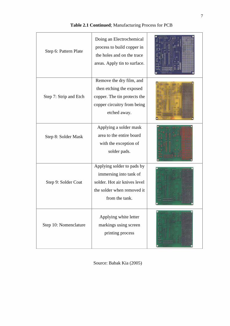
Table 2.1: Manufacturing Process for PCB
Page 16
7
Step 6: Pattern Plate
Doing an Electrochemical
process to build copper in
the holes and on the trace
areas. Apply tin to surface.
Step 7: Strip and Etch
Remove the dry film, and
then etching the exposed
copper. The tin protects the
copper circuitry from being
etched away.
Step 8: Solder Mask
Applying a solder mask
area to the entire board
with the exception of
solder pads.
Step 9: Solder Coat
Applying solder to pads by
immersing into tank of
solder. Hot air knives level
the solder when removed it
from the tank.
Step 10: Nomenclature
Applying white letter
markings using screen
printing process
Table 2.1 Continued; Manufacturing Process for PCB
Source: Babak Kia (2005)
Page 17
8
2.4 ELECTROLESS NICKEL
Electroless is a chemical process which promotes continuous deposition of a
metal onto a surface through an oxidation-reduction chemical reaction, without the use
of an external electrical potential. An internal reducing agent donates electrons to the
positively charged metal ions in solution, thereby reducing the metal and promoting its
deposition onto the catalyzed metal surfaces of the substrate. This reaction is considered
auto-catalytic because it will continue to plate in the presence of source metal ions and a
reducing agent until the board is removed from the plating bath. This gives the plated
part a very uniform deposit and the plating thickness can be controlled easily, even on
complex shapes and internals (Okinaka, 1974).
Therefore, electroless nickel is the autocatalytic deposition of nickel from an
aqueous nickel salt solution onto a substrate and the corresponding oxidation of
hypophosphite anions to phosphite ions with the evolution of hydrogen gas at the
catalytic surface
The purposes of electroless nickel plating are to improving the corrosion
resistance, providing a uniform and dense coating, increasing the surface hardness of the
material, and in many cases, maintains the same surface finish the material had before
plating.
Electroplating bath consists of a series of components to produce a desired layer of
nickel thickness as shown below:
a) Source of nickel ions
The metal source serves as the provider of nickel ions. It is introduced as metal
salts and the most widely used and preferred source of nickel is nickel sulphate.
Other nickel salts include nickel chloride, nickel acetate and the ideal source of
nickel ions is nickel salt of hypophosphorus acid, Ni (H2PO2)2.
b) Reducing agent
Reducing agents for electroless nickel plating are usually phosphate or boron
based with the former more widely used. The reducing agents provide reaction
energy for the nickel to deposit.
Page 18
9
c) Complexing agent
Complexing agents assist in preventing the pH of the electroless nickel solution
from decreasing too fast. They are also required to prevent precipitation of
nickel salts into precipitated phosphites and reduce the concentration of free
nickel ions. There are several types of complexing agents used and they include
citrate, glycolate or lactate ions which come in monodendate, bidendate,
tridendate and quadridentate forms of anions. The rate of the nickel deposition is
proportional to the stability constant of the complexing agent. The lower plating
bath is generally explained by the ‘tying-up’ process of the nickel ions and
releases only a small fraction of free nickel ions.
d) Stabilizer
Stabilizers are added to reduce the spontaneous decomposition rate of the
Electroless Nickel plating solution. Stabilizers raise issues of decreased
deposition rate of the plating process. Many Electroless Nickel plating processes
have employed stabilizers which can be divided into the following groups
(Mallory, 1990):
i. Compound of group VI elements
ii. Compound Containing oxygen
iii. Heave metal cations
iv. Unsaturated organic acids
e) pH adjuster
Rapid increase of the hydrogen ion concentration in the plating bath will
increase the acidity of the bath. This can be measured by the decrease of the pH
value. Reduced pH will slow down the plating rate considerably and eventually
stop the plating. The impairing of hypophosphite reduction power in low pH
condition causes this condition. In addition, the newly plated nickel deposition
will dissolve into the highly acidic plating solution at an increasing dissolution
rate and eventually equal the nickel deposition rate. Therefore, it is necessary to
adjust and maintain the pH value throughout the plating process in order to
obtain a satisfactory thickness (Pecht, 1990). The adjustment of pH can be done
Page 19
10
by periodic or continuous addition of a soluble alkali hydroxide or a soluble
alkaline salt.
Figure 2.1 shows the formation of Nickel ions when Copper substrate was
subjected with Electroless Nickel plating. Nickel ions will form a Nickel layer and coat
the Copper substrate.
Figure 2.1: Electroless Nickel Plating
Source: Dan Slocum (2003)
2.5 ELECTROLESS NICKEL / IMMERSION GOLD (ENIG)
ENIG is an electroless nickel layer capped with a thin layer of immersion gold.
It is a multifunctional surface finish, which is applicable to soldering, aluminum wire
bonding, press fit connections, and also as a contact surface. The immersion gold
protects the underlying nickel from oxidation or passivation over its intended life. The
gold layer is very thin and not intended to provide the main structure of the track. It just
acts as a protective coating for the nickel to prevent it tarnishing before it is soldered.
Gold is extremely resistant to corrosion so ENIG has several good points. It can be
touched with bare fingers without tarnishing, has a very long shelf life, and the pads or
tracks are very flat and square-edged, which is something that very important for fine
pitch surface mount part.
ENIG is formed by the deposition of electroless nickel on a catalyzed copper
surface followed by a thin layer of immersion gold. The IPC ENIG Specification 4522
specifies that the electroless nickel thickness shall be 3 to 6 μm. The minimum
Page 20
11
immersion gold thickness shall be 0.05 μm which are at four sigma (standard deviation)
below the mean, the typical range is 0.075 to 0.125 μm. Higher gold thickness would
normally require extended solution dwell time and /or increased solution temperature
(Dan, 2003).
The ENIG deposition process is fairly complex; it requires a clean copper
surface free of solder mask residues as well as free of any copper/tin intermetallic (tin is
used as an etch resist and is stripped before ENIG). Solder mask for ENIG plating must
be adherent and completely cured (cross-linked) to withstand the high temperature and
prolonged dwell in the electroless nickel bath and in the immersion gold bath
(Dan,2003). Figure 2.2 shows the formation of Nickel ions and gold ions when Copper
substrate was subjected to the ENIG plating.
Figure 2.2: Electroless Nickel / Immersion Gold Plating
Source: Dan Slocum (2003)
2.6 INTERMETALLIC COMPOUND (IMC)
IMC have often been observed at or near the solder/substrate interface as well as
in the interior of solder joints. Its can be defined as a mixture in specifics proportion of
two metallic elements that form a periodic crystalline structure different from those of
the original elements. Unlike conventional metal alloys, the particular structure of
intermetallic compounds is caused because of the respectively larger strength of
bounding between the respective unlike atoms than between like atoms. This particular
structure of intermetallic compounds gives them some mechanical properties such as
Page 21
12
high melting points and great strength (particularly at high temperatures), but poor
ductility (Sandström, 2002).
Intermetallic compounds usually form between two metal elements that
comprise of a limited mutual solubility through diffusion. These compounds possess a
composition of a certain stoichiometric ratio of the two elements (Gilleo, 2004). The
new composition has a different crystal structure from those of their elemental
components. The interface of tin and copper when examined in a cross section would
reveal a superimposed layer consisting of compounds having certain copper/tin ratio as
shown in Figure 2.3.
Figure 2.3: Formation of IMC layer between solder and copper
Source: Madeni (2003)
There are some key facts about intermetallic formations that should be
illustrated in order to prevent reductions in reliability, solderability and yield.
Intermetallics are necessary, but it can result in embrittled joints and unsolderable
components or circuit boards.
When solder comes in contact with a common metal substrate for a sufficient
amount of time at a high enough temperature, intermetallic compounds may form.
Below a solder’s liquidus temperature, formation is primarily a solid state diffusion
process and thus depends highly on temperature and time. While solder is in a molten
state, the solubility of the element from substrate into molten solder accelerates the rate
of intermetallic formation.
Page 22
13
There are various factors which influence the intermetallic formation, the
composition of the compound and its morphology:
i. The metallurgical reactivity of a solder with a substrate
ii. Soldering (reflow) peak temperature
iii. Dwell time at peak temperature
iv. The surface condition of a substrate
v. The post- soldering storage and service conditions
Apart from above factors, the selection of solder alloy and surface finish play
important role as well.
2.6.1 Types of IMC formations in Solder Joints
Formation of IMC at the solder interface is primarily governed by the material
of the solder, surface finish and substrate metal pad. The most commonly found IMCs
are from copper-tin lead-frame, where the copper is the base material and the tin comes
from solders. Lead rarely forms intermetallic in solder joints but commonly encountered
elements that may form IMC with tin which include copper, nickel, silver and gold.
The possible IMC forms at the interfacial of solder and substrate is determined
by solder material used, substrate material and surface finish covered on the substrate.
Table 2.2 shows the possible intermetallic phases in various lead frame system.
Table 2.2: Possible intermetallic phases in various lead-frame system
Lead-frame system Intermetallic
Copper-tin Cu3Sn, Cu6Sn5
Nickel-tin Ni3Sn2,Ni3Sn4,Ni3Sn
Gold-tin AuSn,AuSn3,AuSn4
Silver-tin (Lead-free solder) Ag3Sn
Source: Madeni (2003)
The most common solder/substrate intermetallic compound is tin/copper
(Sn/Cu). The growth of the total intermetallic layer is influenced by the synergy
information and growth between η (Cu6Sn5) and ε (Cu3Sn) phases. Cu6Sn5 (η- phase) is
the first to form at lower temperatures (< 170°C) and is essential for good solder
adhesion to the copper substrate. This compound grows rapidly but once the metals
solidify, it will slow sharply. The ε-phase has been shown to grow at the expense of the
Page 23
14
η-phase, and has higher activation energy of formation, so growth of ε is more
predominant at higher temperatures. The mechanisms for intermetallic formation are
also greatly influenced by the interdiffusion characteristics of tin and copper.
In Nickel/gold-tin system, the eutectic solder forms a strong attachment to
underlying nickel by forming the Ni3Sn2, Ni3Sn4, Ni3Sn intermetallic while the Au
dissolves into the molten solder, and forms fine, needle-shaped AuSn4 intermetallic
precipitates that are retained in a dense distribution in the bulk of the solder joint after it
has solidified (Glazer, 1991).
When lead free solder, such as Sn/Ag or pure Sn is used on a copper substrate,
the Ag3Sn plate intermetallic is formed while Cu6Sn5 compound forms as the bottom
layer. Large Ag3Sn plate formation is found to be substantially reduced in alloys with a
silver content less than 3 wt % (Sung, 2004). Because of the relatively low fraction (3-5
wt%) of alloying elements, these intermetallic structures comprising a small portion of
the area within the solder joint. The morphology are varies, exhibiting a round, lath like,
blocky, or needle like structure. Studies have shown, however, that intermetallic
structures at the interface, such as tin-copper, grow slower in some tin-based lead-free
solders than with their leaded counterpart. It is believed that lead plays a part in
enhancing intermetallic growth when subjected to thermal exposure.
2.7 SOLDERING
Soldering is a process in which two or more metal items are joined together by
melting and flow a filler metal (solder) into the joint, the filler metal having a lower
melting point than the workpiece. Soldering basically is use to make electrical
connection between electrical device like transistor, diodes, capacitors, resistance and
etc. Its also provide physical connection between the component and its supporting
printed circuit board (Woodgate, 1983).
Solder chemically reacts with other metals to form different alloy. There are four
basic element involve in soldering process; base metal, flux, solder and heat. A base
metal is a metal that contacts the solder and forms an intermediate alloy. When
attaching electronic components to a printed circuit board, the component's leads or pins
and board's metallic circuitry at the base metals and will contact with the solder. Many
metals, such as copper, bronze, silver, brass, and some steels, readily react with solder
Page 24
15
to form strong chemical and physical bonds. There is a direct relationship with the level
of surface oxidation on the base metal and how readily solder will react with it. The
more oxidation is present, the weaker the solder bond will be (Hwang, 2002).
Flux is often applied as a liquid to the surface of the base metals prior to
soldering. The first and primary purpose of flux is to stop the base metals from
oxidizing while they are being heated to the soldering temperature. The flux covers the
surface to be soldered, shielding it from oxygen and thereby preventing oxidation
during heating. Most fluxes have an acidic element that is used to remove the oxidation
already present on the base metal. Using a strong acid, it would be possible to virtually
completely clean off the oxidation layer. When the liquid solder is applied, the flux
must readily to move out of the way so the solder can come directly contact with the
base metal. During this process some of the flux inevitably combines with the solder.
Solder is typically transported and sold in solid form. Common forms of solder
including chips, bars, and wire (often with a core of flux), each of it which has
advantages in different soldering processes. A common process called reflow soldering
is use for a solder paste. Solder paste is a substance with a cream-like consistency made
up of solder, flux, and some carrying medium. The material most commonly used for
solder in the electronics industry is a tin-lead alloy. Tin-lead alloys have relatively low
melting point and can be produced at a low cost in comparison with other alloys with
similar properties.
2.7.1 Soldering Methods
There are various soldering techniques developed throughout the growth of
electronic assembly to promote the process capability and productivity. It will be
categorized whether it is performed by hand or by machine. For circuit board, generally
the soldering process will fall into two main categories, which are wave soldering and
reflow soldering. For wave soldering, it is primarily used for soldering through-hole
components on PCBs where the electronic components are inserted prior to application
of solder. For reflow soldering, it is used for soldering SMD (Surface Mount Device)
components on to PCBs. The electronic components are mounted after the application
of solder.


![STRATISS - CVE-2018-8453 - Sanitized...LookingGlass STRATISS: Confidential | 2 CVE-2018-8453 Being Sold on Exploit[.]in On December 6, 2018, Russian threat actor X advertised the sale](https://static.documents.pub/doc/80x56/5f6498cbf1e0d45aa74d7626/stratiss-cve-2018-8453-sanitized-lookingglass-stratiss-confidential-2.jpg)


