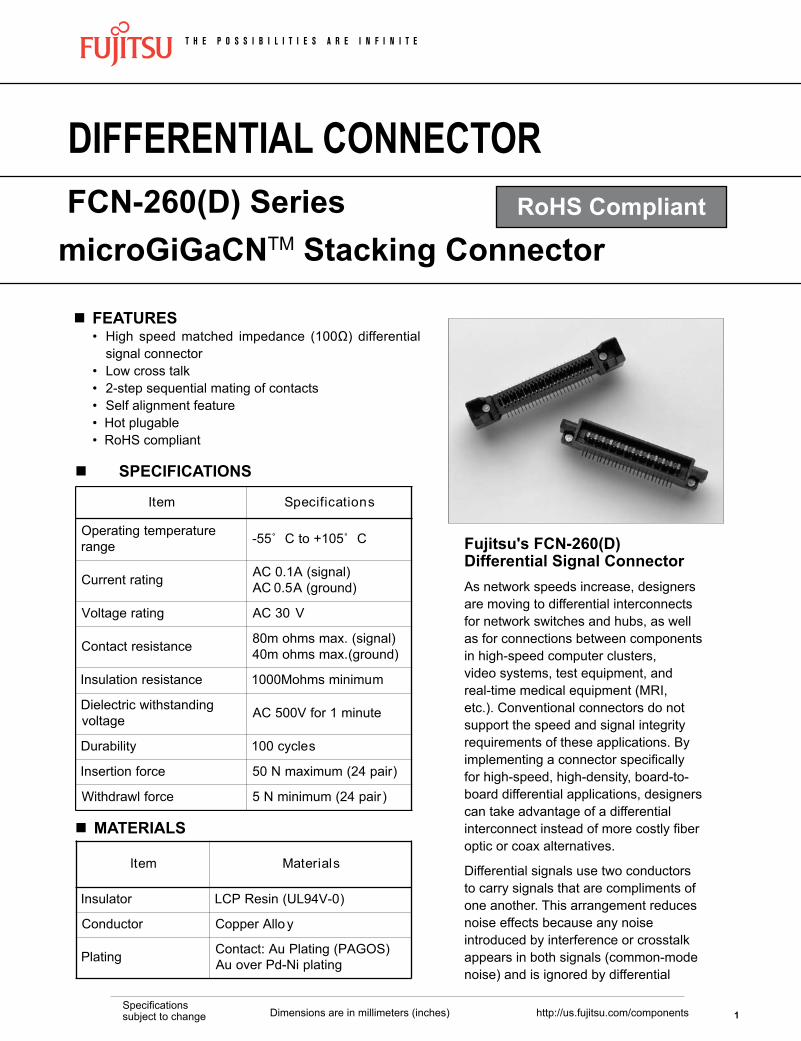
Dimensions are in millimeters (inches) http://us.fujitsu.com/components Specifications subject to change DIFFERENTIAL CONNECTOR FCN-260(D) Series microGiGaCN TM Stacking Connector n FEATURES • High speed matched impedance (100Ω) differential signal connector • Low cross talk • 2-step sequential mating of contacts • Self alignment feature • Hot plugable • RoHS compliant n SPECIFICATIONS n MATERIALS Fujitsu's FCN-260(D) Differential Signal Connector As network speeds increase, designers are moving to differential interconnects for network switches and hubs, as well as for connections between components in high-speed computer clusters, video systems, test equipment, and real-time medical equipment (MRI, etc.). Conventional connectors do not support the speed and signal integrity requirements of these applications. By implementing a connector specifically for high-speed, high-density, board-to- board differential applications, designers can take advantage of a differential interconnect instead of more costly fiber optic or coax alternatives. Differential signals use two conductors to carry signals that are compliments of one another. This arrangement reduces noise effects because any noise introduced by interference or crosstalk appears in both signals (common-mode noise) and is ignored by differential m e t I s n o i t a c i f i c e p S e r u t a r e p m e t g n i t a r e p O e g n a r C ˚ 5 0 1 + o t C ˚ 5 5 - g n i t a r t n e r r u C ) l a n g i s ( A 1 . 0 C A ) d n u o r g ( A 0.5 C A g n i t a r e g a t l o V V 0 3 C A e c n a t s i s e r t c a t n o C ) l a n g i s ( . x a m s m h o m 0 8 ) d n u o r g ( max. s m h o m 0 4 e c n a t s i s e r n o i t a l u s n I m u m i n i m s m h o M 0 0 0 1 g n i d n a t s h t i w c i r t c e l e i D e g a t l o v e t u n i m 1 r o f V 0 0 5 C A y t i l i b a r u D s e l c y c 0 0 1 e c r o f n o i t r e s n I ) r i a p 4 2 ( m u m i x a m N 0 5 e c r o f l w a r d h t i W ) r i a p 4 2 ( m u m i n i m N 5 m e t I s l a i r e t a M r o t a l u s n I ) 0 - V 4 9 L U ( n i s e R P C L r o t c u d n o C y o l l A r e p p o C g n i t a l P ) S O G A P ( g n i t a l P u A : t c a t n o C g n i t a l p i N - d P r e v o u A RoHS Compliant
Transcript
Dimensions are in millimeters (inches) http://us.fujitsu.com/componentsSpecifications subject to change
Differential COnneCtOr fCn-260(D) Series microGiGaCnTM Stacking Connector
n featureS • High speed matched impedance (100Ω) differential
signal connector • Low cross talk • 2-step sequential mating of contacts • Self alignment feature • Hot plugable • RoHS compliant
n SpeCifiCatiOnS
n MaterialS
fujitsu's fCn-260(D) Differential Signal Connector
As network speeds increase, designers are moving to differential interconnects for network switches and hubs, as well as for connections between components in high-speed computer clusters, video systems, test equipment, and real-time medical equipment (MRI, etc.). Conventional connectors do not support the speed and signal integrity requirements of these applications. By implementing a connector specifically for high-speed, high-density, board-to-board differential applications, designers can take advantage of a differential interconnect instead of more costly fiber optic or coax alternatives.
Differential signals use two conductors to carry signals that are compliments of one another. This arrangement reduces noise effects because any noise introduced by interference or crosstalk appears in both signals (common-mode noise) and is ignored by differential
2Dimensions are in millimeters (inches) http://us.fujitsu.com/componentsSpecifications subject to change
networking hubs incorporate many boards that must be interconnected via short-run cables. These internal cables often have to transfer data at speeds significantly higher than those of the actual network, so even today's 10/100-Mbit networks need high-speed internal interconnects with excellent signal integrity. In addition, any system that uses an external fiber optic connector probably requires an internal, board-to-board connector system that works at the highest possible speeds.
Fiber optic and coax interconnect systems obviously meet the internal performance requirements, but the cost is high. Differential interconnects meet both the performance and cost goals but until recently, no connectors were available that provided high-density connections at gigabit speeds. In addition, connector test methodologies from the past cannot give reliable and repeatable results of the differential connector's performance in high-speed systems. Therefore, new test methodologies must be developed based on the unique characteristics of these emerging high-speed applications.
High-speed differential interconnect characterizationIn the past, connector manufacturers "de-imbedded" the connector from the test PCB's to show just the electrical characteristics of the connector and did not include any parasitic effects associated with solder joints on a through hole contact lead, or the effects of the contact post (compliant or non-compliant pin) in a plated through hole. While this test methodology was acceptable for slower system speeds, today's differential interconnects demand much more focused attention on system and board effects.
The requirements for testing today's high-speed differential interconnects are demanding with good reason. Connectors and other traditionally "electrically small" components are no longer small when considering presently available signaling technologies with 100ps risetimes and multi-gigabit data rates. Among these requirements are very well-designed test boards needed for accurate measurement and characterization. This data is
receivers. With noise voltages less of a problem, differential signals can use a small voltage swing that switches between LOW and HIGH values extremely quickly --hence the appeal of differential signals for high-speed networking and clustering.
Differential connector characteristics can exceed the requirements of upcoming 1-Gbit applications and extend to next-generation applications at speeds upwards of 4.4 Gbps. As a result, system and board vendors who adopt such a connector can look forward to legacy usage that spans multiple product generations.
The signal transmission path of connectors has not always been a critical issue when choosing an interconnect method because the connector's electrical signal path is short compared to cables or printed circuit board assemblies. In applications utilizing high-frequency signals, however, connectors can have a significant effect on signal integrity. Connectors for high-speed applications must be designed to achieve optimal performance through the minimization of crosstalk and susceptibility to noise influences.
Differential signal applicationsThe shift from mainframe environments to networked client/server enterprises has made networks a critical bottleneck for improving system performance. Emerging technologies such as high-speed server farms, video conferencing, and greater use of graphical interfaces is pushing networks toward performance of 1 Gbit/sec and higher. The IEEE 802 committee is releasing 1.028-Gbit Ethernet standards to meet this requirement.
One of the key challenges for switch, hub, video equipment, and server manufacturers is to find a board-to-board connector system that allows signals to transfer at gigabit speeds over an affordable interconnect system that furnishes specific matched-impedance characteristics. Applications such as servers are now moving to extremely high-speed interfaces (often based on Fibre Channel) between computer backplanes and disk subsystems that require advance interconnects between boards. Similarly,
microGiGaCnTM fCn-260 (D) Series
Dimensions are in millimeters (inches) http://us.fujitsu.com/componentsSpecifications subject to change
used to develop SPICE or other models and to provide detailed data to the design community. Typical high-frequency test boards designed by Fujitsu include:
l well-controlled impedance, matched-Iength test traces (with "real-world" widths and spacings)
l calibration/reference lines that mimic the test traces
l connector region entities (pads, pins, vias) that reflect actual system board implementations
l low discontinuity test connectors (these give access to the measurement equipment) of sufficient bandwidth to meet the testing needs (e.g. SMA, 55MB, etc.)
Differential pairs must be well-matched in order to minimize skew and maintain the proper impedance. Calibration lines of lengths "L" (where L is the length of the test traces between the article under test and the test connectors) and 2L provide the opportunity to calibrate out the board effects (if necessary) as well as to make "reference" measurements to test the goodness of an interconnect. These reference measurements are especially important when determining transmission fidelity. Fujitsu Components attempts to use standard, commonly available FR-4 type board materials (better performers than some believe) whenever possible; however, there are times when so-called "low loss" board materials may be required, such as for long paths running at gigabit speeds.
In addition to very good test articles, test equipment must be selected that will provide for the measurements required at the bandwidths needed. Measurements may be completed for differential interconnects running at 100 Mbps, 625 Mbps, 1 Gbps, 2.5 Gbps or beyond depending on the system being designed. Fujitsu Components typically measures for single-ended and differential impedance (using a "TDR"), transmission fidelity, crosstalk, and eye pattern performance among other measures of quality. Typical transmission parameters quantified
include signal edge and amplitude losses, skews, propagation delays, and interconnect bandwidth. At times, frequency domain data (such as S-parameters) adds insight into these measurements and may be preferred by some customers. However, differential measurements in the frequency domain must be approached with caution and specialized knowledge.
microGiGaCnTM fCn-260 (D) Series
Dimensions are in millimeters (inches) http://us.fujitsu.com/componentsSpecifications subject to change
Figure 1
Figure 2
+
-
+
-
1.27 mm
+
-
0.75 mm1.5 mm
Patent pending
Ground/Power contactDifferential pair contact
Virtual ground plane
Sectional View (Connection area)Basic Concept for Differential Transfer
Edge coupleddifferential pairs
SMA connector footprints
Drive pairs Measurementpair
S1+ S1- S2+ S2- S3+ S3-
PCB Routing -Test Card
SMA connectorfoot print
Drive pairs Measurementpair
S1+ S1- S2+ S2- S3+ S3-
Adapter card socketfoot printcard
6“ test pattern 3” test patternEdge coupleddifferential pairs
PCB Routing - Test Card
microGiGaCnTM fCn-260 (D) Series
Dimensions are in millimeters (inches) http://us.fujitsu.com/componentsSpecifications subject to change
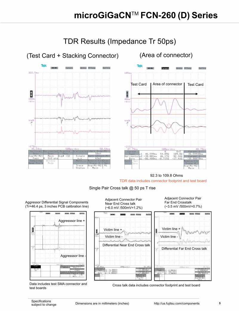
Single Pair Cross talk @ 50 ps T rise
Aggressor Differential Signal Components(Tr=46.4 ps, 3 inches PCB calibration line)
Adjacent Connector PairNear End Cross talk(~6.0 mV /500mV=1.2%)
Adjacent Connector PairFar End Crosstalk(~3.5 mV /500mV=0.7%)
Aggresssor line -
Aggresssor line +
Data includes test SMA connector and test boards
Victim line +
Victim line -
Differential Near End Cross talk
Cross talk data includes connector footprint and test board
Differential Far End Cross talk
Victim line +
Victim line -
TDR Results (Impedance Tr 50ps)
(Test Card + Stacking Connector) (Area of connector)
Test Card
TDR data includes connector footprint and test board92.3 to 109.8 Ohms
Area of connector Test Card
microGiGaCnTM fCn-260 (D) Series
6Dimensions are in millimeters (inches) http://us.fujitsu.com/componentsSpecifications subject to change
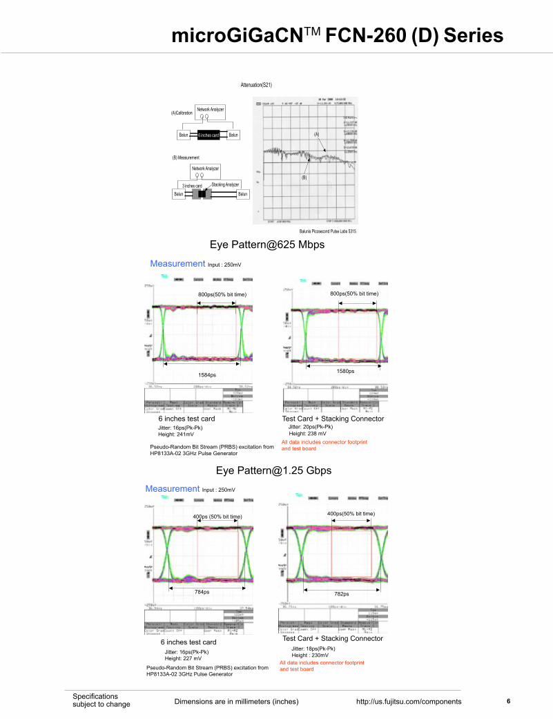
Eye Pattern@625 Mbps
Pseudo-Random Bit Stream (PRBS) excitation fromHP8133A-02 3GHz Pulse Generator
Test Card + Stacking Connector
Measurement Input : 250mV
6 inches test card
800ps(50% bit time)
1584ps
Jitter: 20ps(Pk-Pk)Height: 238 mV
All data includes connector footprint and test board
north and South americaFujitsu Components America, Inc.250 E. Caribbean DriveSunnyvale, CA 94089 U.S.A.Tel: (1-408) 745-4900Fax: (1-408) 745-4970Email: [email protected]: http://www.fujitsu.com/us/services/edevices/components/
Fujitsu Components America or its affiliates do not warrant that the content of datasheet is error free. In a continuing effort to improve our products Fujitsu Components America, Inc. or its affiliates reserve the right to change specifications/datasheets without prior notice.Rev. September 24, 2008