25
Diffraction methods and electron microscopy Outline and Introduction to FYS4340 and FYS9340
| Date post: | 24-Dec-2015 |
| Category: |
Documents |
| Upload: | ethelbert-parrish |
| View: | 224 times |
| Download: | 2 times |
Diffraction methods and electron microscopy
Outline and Introduction to FYS4340 and FYS9340
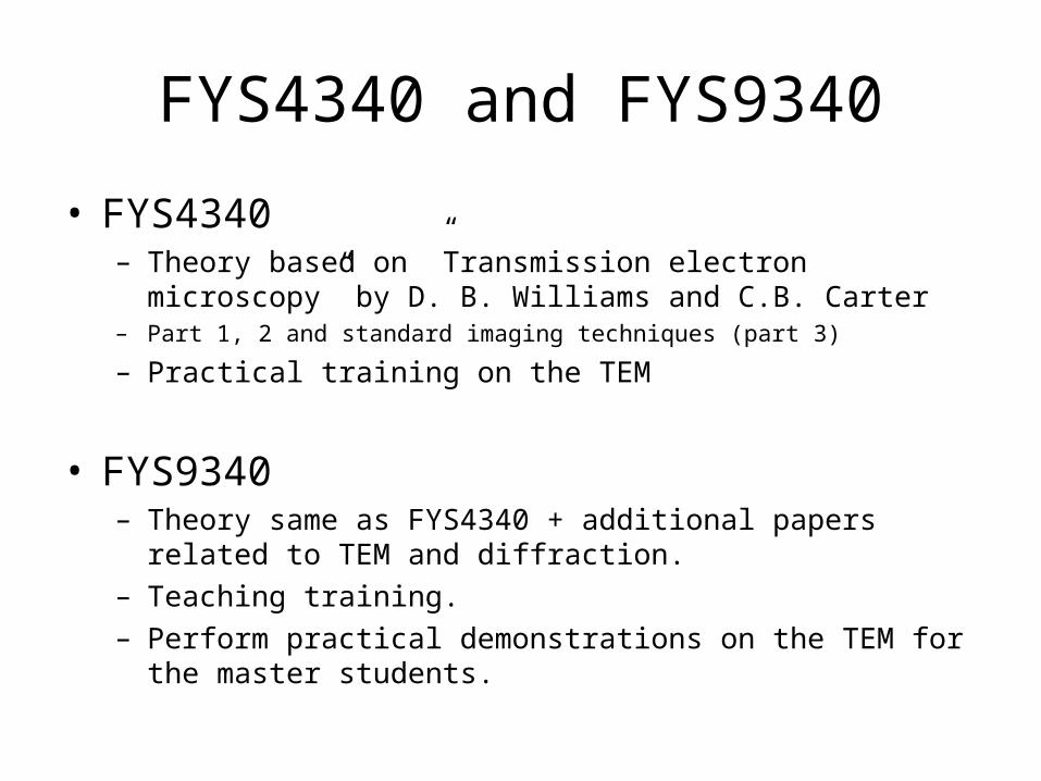
FYS4340 and FYS9340
• FYS4340– Theory based on ”Transmission electron microscopy” by D. B. Williams
and C.B. Carter– Part 1, 2 and standard imaging techniques (part 3)
– Practical training on the TEM
• FYS9340– Theory same as FYS4340 + additional papers related to TEM and
diffraction.– Teaching training.– Perform practical demonstrations on the TEM for the master students.
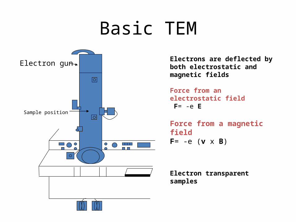
Basic TEM
Electron gun
Sample position
Electrons are deflected by both electrostatic and magnetic fields
Force from an electrostatic field F= -e E
Force from a magnetic field F= -e (v x B)
Electron transparent samples
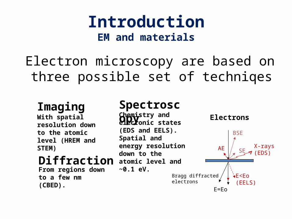
IntroductionEM and materials
Electron microscopy are based on three possible set of techniqes
Imaging
Diffraction
SpectroscopyWith spatial resolution down to the atomic level (HREM and STEM)
Chemistry and elecronic states (EDS and EELS).Spatial and energy resolution down to the atomic level and ~0.1 eV.
From regions down to a few nm (CBED).
Electrons
E<Eo(EELS)
BSE
SEAE X-rays (EDS)
E=Eo
Bragg diffracted electrons
15/1-08 MENA3100
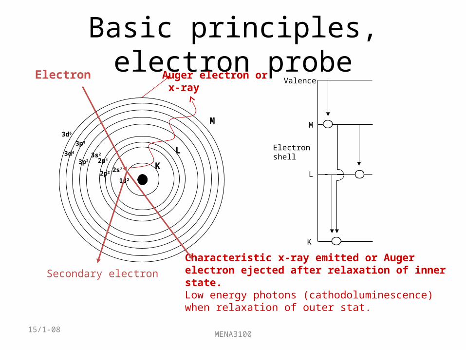
Basic principles, electron probeValence
K
L
M
Electronshell
Characteristic x-ray emitted or Auger electron ejected after relaxation of inner state. Low energy photons (cathodoluminescence)when relaxation of outer stat.
K
L
M
1s2
2s22p2
2p43s2
3p2
3p4
3d4
3d6
Auger electron or x-ray
Secondary electron
Electron
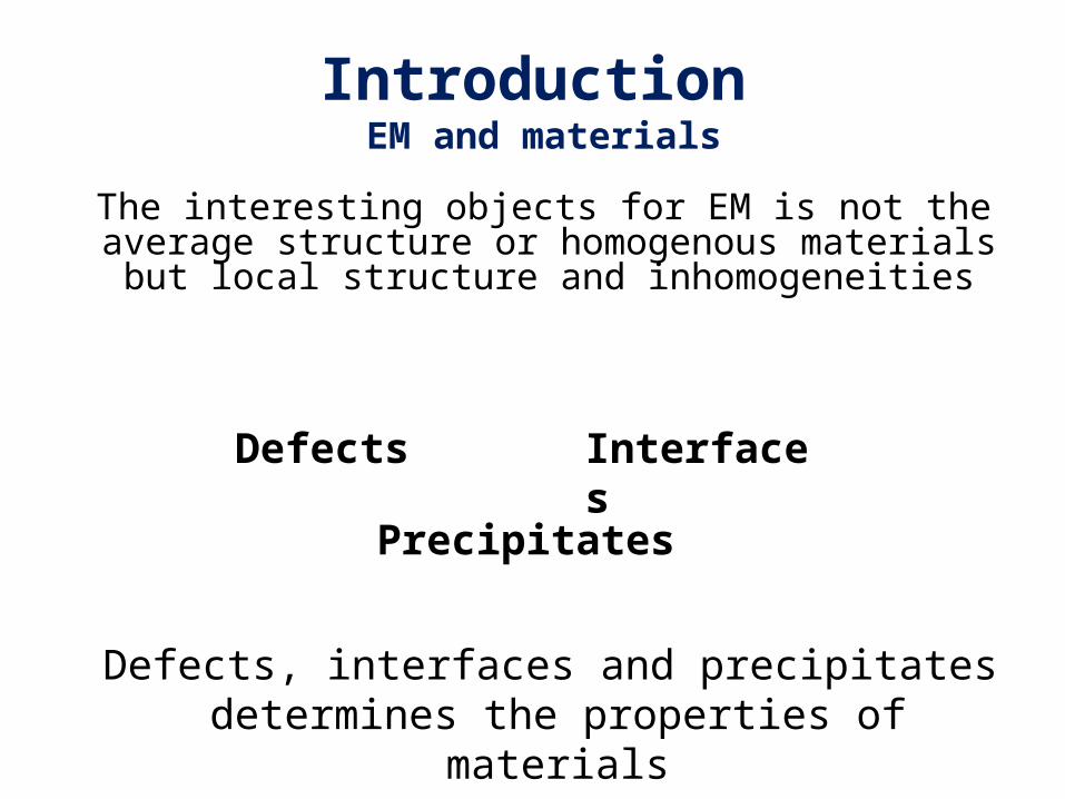
Introduction EM and materials
The interesting objects for EM is not the average structure or homogenous materials but local
structure and inhomogeneities
Defects
Precipitates
Interfaces
Defects, interfaces and precipitates determines the properties of materials
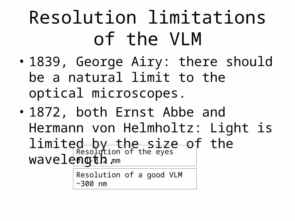
Resolution limitations of the VLM
• 1839, George Airy: there should be a natural limit to the optical microscopes.
• 1872, both Ernst Abbe and Hermann von Helmholtz: Light is limited by the size of the wavelength.
Resolution of the eyes 0.1-0.2 mm
Resolution of a good VLM ~300 nm
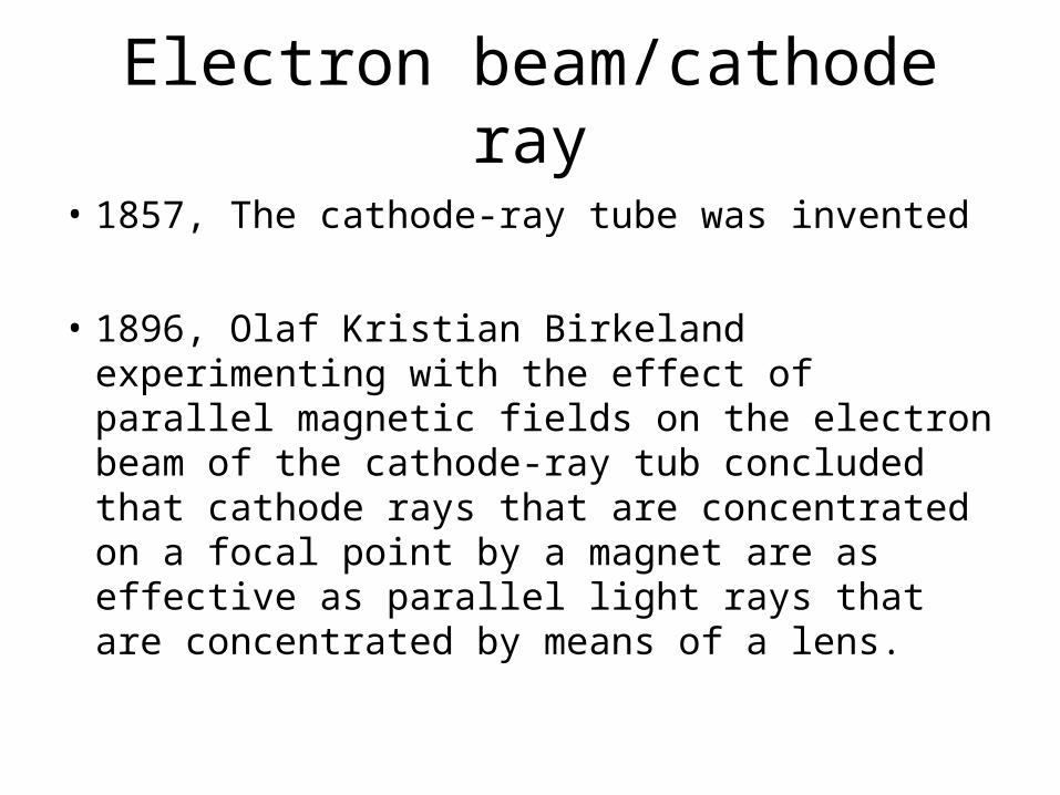
Electron beam/cathode ray
• 1857, The cathode-ray tube was invented
• 1896, Olaf Kristian Birkeland experimenting with the effect of parallel magnetic fields on the electron beam of the cathode-ray tub concluded that cathode rays that are concentrated on a focal point by a magnet are as effective as parallel light rays that are concentrated by means of a lens.
Electron optics
• 1926, Hans Busch, ”Founder of the electron optics” published his theory on the trajectories of electrons in magnetic fields.
• 1928, Graduate student Ruska worked on refining Busch’s work. – The energy of the electrons in the beam was not
uniform resulting in fuzzy images. – Knoll and Ruska were able design and construct
electron lenses and the first realization of an electron microscope.”
Wave nature of electrons
• 1897, J.J. Thomson • Concludes that electrons have particle nature.
• 1924, Louis de Broglie• Hypothesis: Matter on the scale of subatomic particles
possesses wave characteristics. The speed of low-mass subatomic particles, such as electrons, is related to wavelength .
• 1927, Davisson and Germer and Thomson and Reid– Both demonstrated the wave nature of electrons by
independently performing electron diffraction experiments
λ=1.22/E1/2
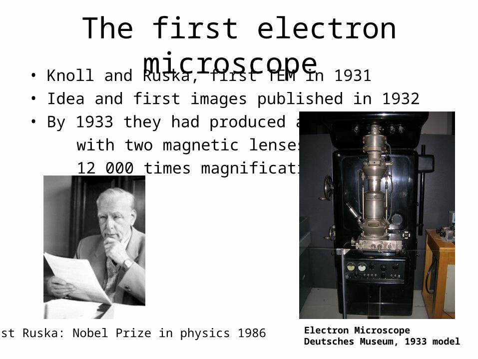
The first electron microscope • Knoll and Ruska, first TEM in 1931• Idea and first images published in 1932• By 1933 they had produced a TEM with two magnetic lenses which gave 12 000 times magnification.
Ernst Ruska: Nobel Prize in physics 1986 Electron Microscope Deutsches Museum, 1933 model
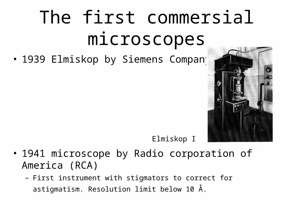
The first commersial microscopes
• 1939 Elmiskop by Siemens Company
• 1941 microscope by Radio corporation of America (RCA)– First instrument with stigmators to correct for astigmatism. Resolution
limit below 10 Å.
Elmiskop I
Developments
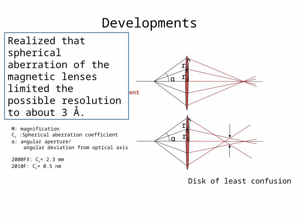
• Spherical aberration coefficient
ds = 0.5MCsα3
M: magnificationCs :Spherical aberration coefficientα: angular aperture/ angular deviation from optical axis
2000FX: Cs= 2.3 mm2010F: Cs= 0.5 nm
r1
r2
Disk of least confusion
α
r1
r2
α
Realized that spherical aberration of the magnetic lenses limited the possible resolution to about 3 Å.
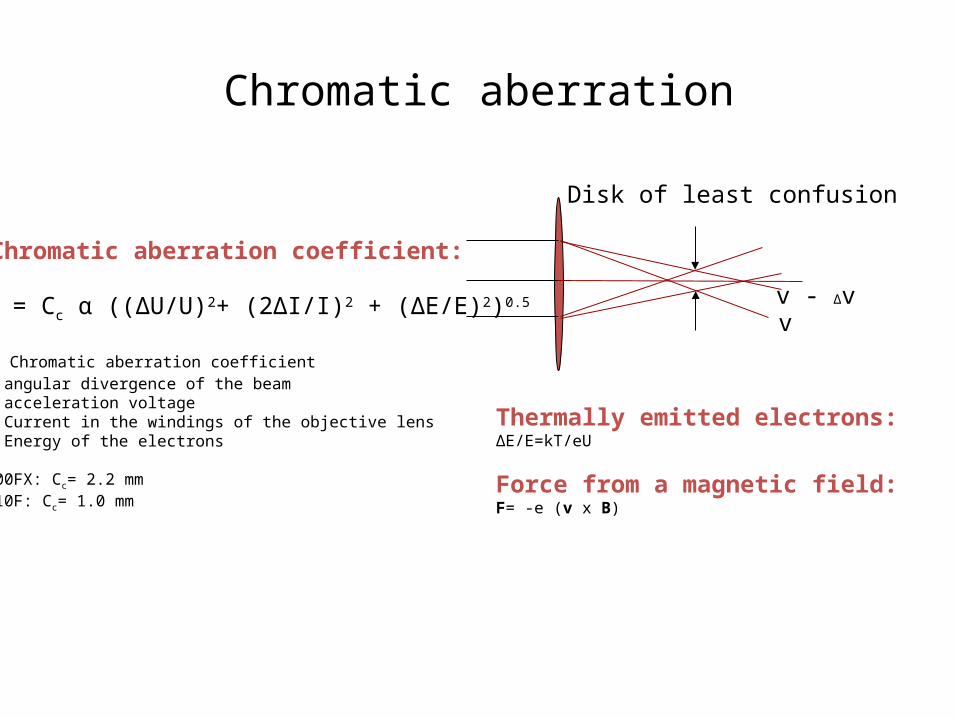
Chromatic aberration
vv - Δvdc = Cc α ((ΔU/U)2+ (2ΔI/I)2 + (ΔE/E)2)0.5
Cc: Chromatic aberration coefficientα: angular divergence of the beamU: acceleration voltageI: Current in the windings of the objective lensE: Energy of the electrons
2000FX: Cc= 2.2 mm2010F: Cc= 1.0 mm
Chromatic aberration coefficient:
Thermally emitted electrons:ΔE/E=kT/eU
Force from a magnetic field:F= -e (v x B)
Disk of least confusion
Developments
~ 1950 EM suffered from problems like: Vibration of the column, stray magnetic fields, movement of specimen stage, contamination.
Lots of improvements early 1950’s.Still far from resolving crystal lattices and making direct atomic observations.
Observations of dislocations and lattice images
• 1956 independent observations of dislocations by:Hirsch, Horne and Wheland and Bollmann
-Started the use of TEM in metallurgy.
• 1956 Menter observed lattice images from materials with large lattice spacings.
• 1965 Komoda demonstrated lattice resolution of 0.18 nm.– Until the end of the 1960’s it was mainly used to test
resolution of microscopes.
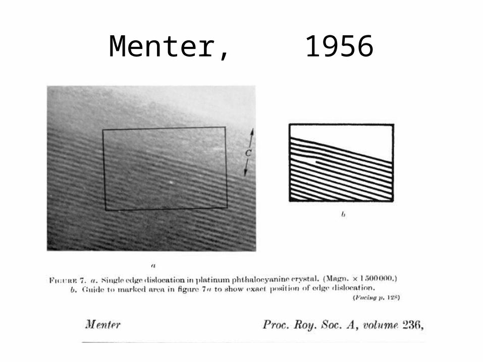
Menter, 1956
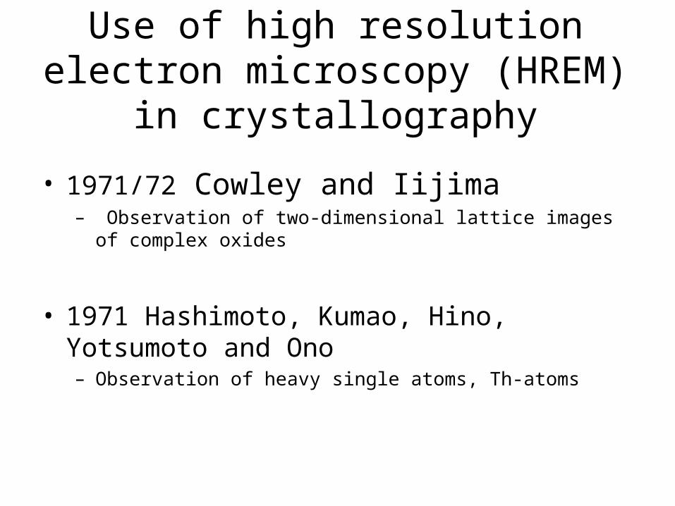
Use of high resolution electron microscopy (HREM) in crystallography
• 1971/72 Cowley and Iijima– Observation of two-dimensional lattice images of complex oxides
• 1971 Hashimoto, Kumao, Hino, Yotsumoto and Ono– Observation of heavy single atoms, Th-atoms
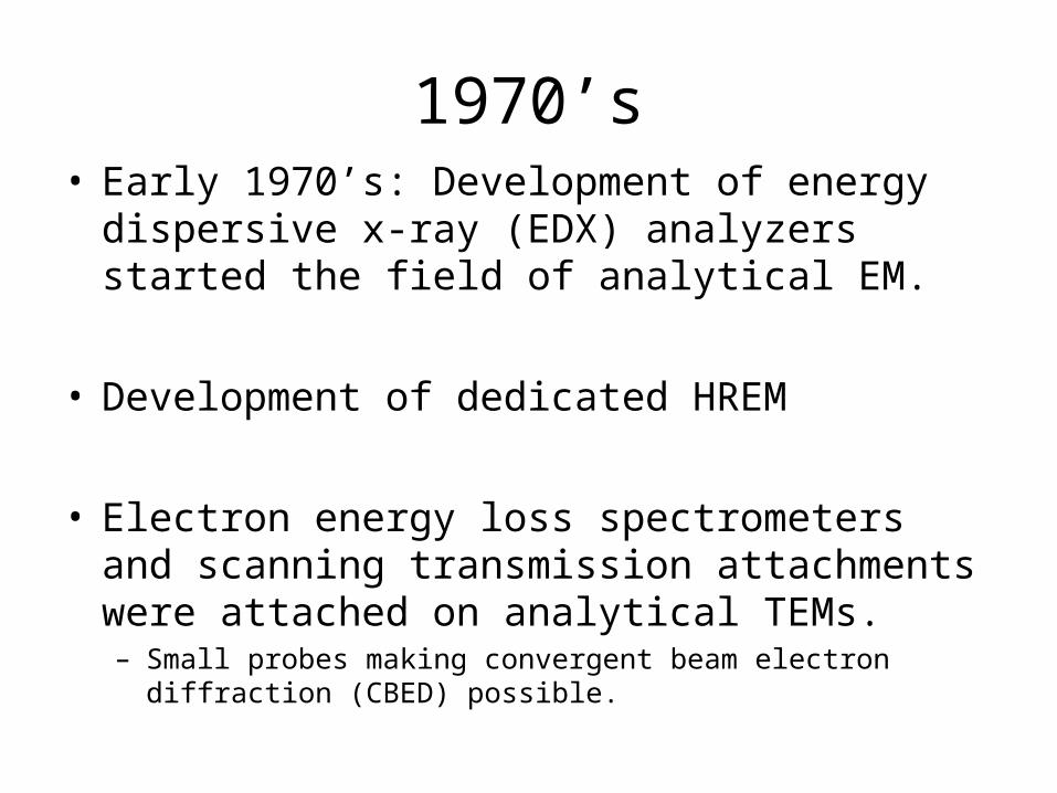
1970’s• Early 1970’s: Development of energy dispersive x-ray
(EDX) analyzers started the field of analytical EM.
• Development of dedicated HREM
• Electron energy loss spectrometers and scanning transmission attachments were attached on analytical TEMs.– Small probes making convergent beam electron diffraction (CBED)
possible.
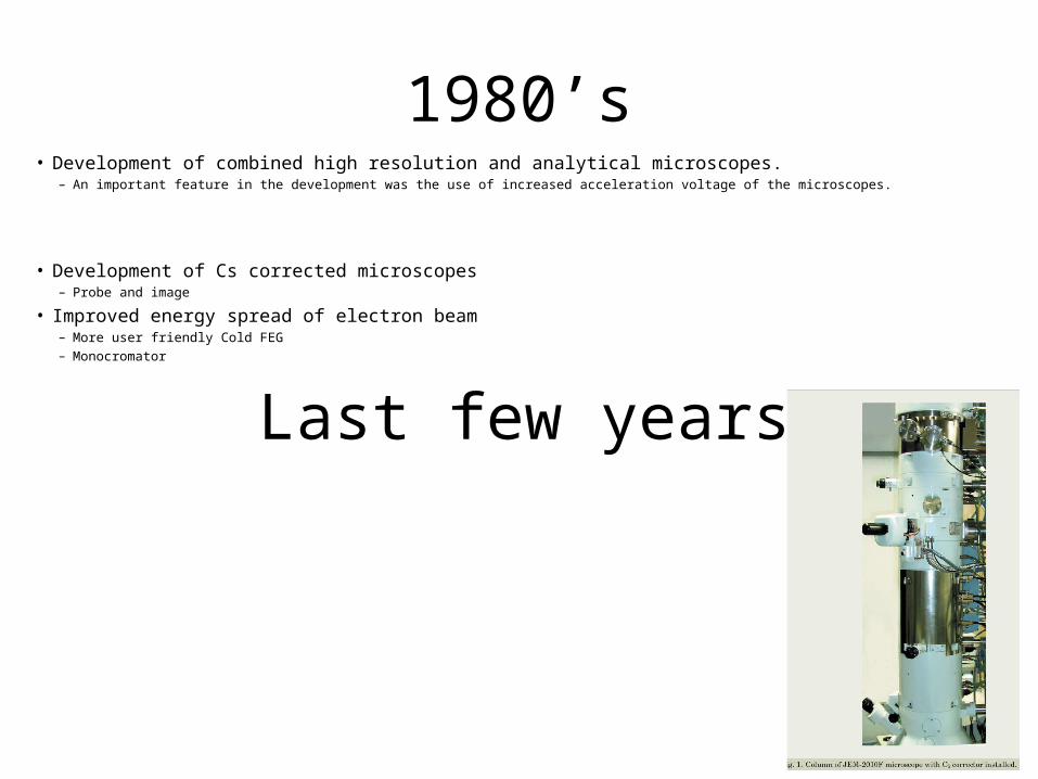
1980’s• Development of combined high resolution and analytical microscopes.
– An important feature in the development was the use of increased acceleration voltage of the microscopes.
• Development of Cs corrected microscopes– Probe and image
• Improved energy spread of electron beam– More user friendly Cold FEG – Monocromator
Last few years
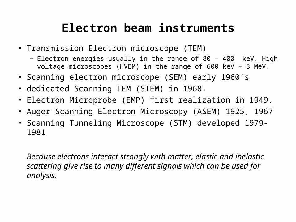
Electron beam instruments
• Transmission Electron microscope (TEM)– Electron energies usually in the range of 80 – 400 keV. High voltage
microscopes (HVEM) in the range of 600 keV – 3 MeV.
• Scanning electron microscope (SEM) early 1960’s• dedicated Scanning TEM (STEM) in 1968.• Electron Microprobe (EMP) first realization in 1949.• Auger Scanning Electron Microscopy (ASEM) 1925, 1967• Scanning Tunneling Microscope (STM) developed 1979-1981
Because electrons interact strongly with matter, elastic and inelastic scattering give rise to many different signals which can be used for analysis.
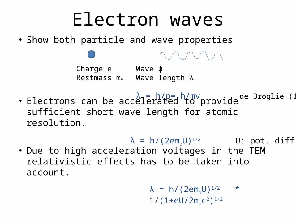
Electron waves• Show both particle and wave properties
• Electrons can be accelerated to provide sufficient short wave length for atomic resolution.
• Due to high acceleration voltages in the TEM relativistic effects has to be taken into account.
Charge eRestmass mo
Wave ψWave length λ
λ = h/p= h/mv de Broglie (1925)
λ = h/(2emoU)1/2 U: pot. diff.
λ = h/(2emoU)1/2 * 1/(1+eU/2moc2)1/2
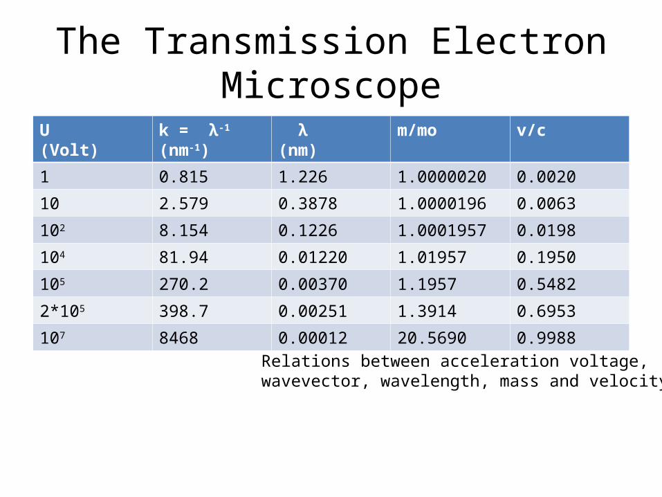
The Transmission Electron Microscope
U (Volt) k = λ-1 (nm-1) λ (nm) m/mo v/c
1 0.815 1.226 1.0000020 0.0020
10 2.579 0.3878 1.0000196 0.0063
102 8.154 0.1226 1.0001957 0.0198
104 81.94 0.01220 1.01957 0.1950
105 270.2 0.00370 1.1957 0.5482
2*105 398.7 0.00251 1.3914 0.6953
107 8468 0.00012 20.5690 0.9988
Relations between acceleration voltage, wavevector, wavelength, mass and velocity
MENA3100 V08
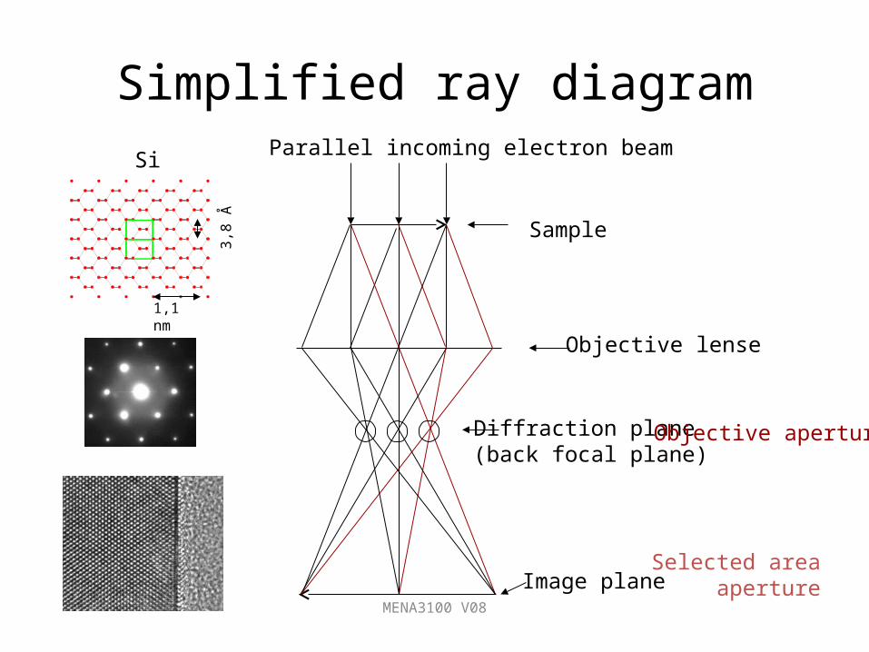
Objective lense
Diffraction plane(back focal plane)
Image plane
Sample
Parallel incoming electron beamSi
a
b
cP
ow
derC
ell 2.0
1,1 nm
3,8
Å
Objective aperture
Selected area aperture
Simplified ray diagram
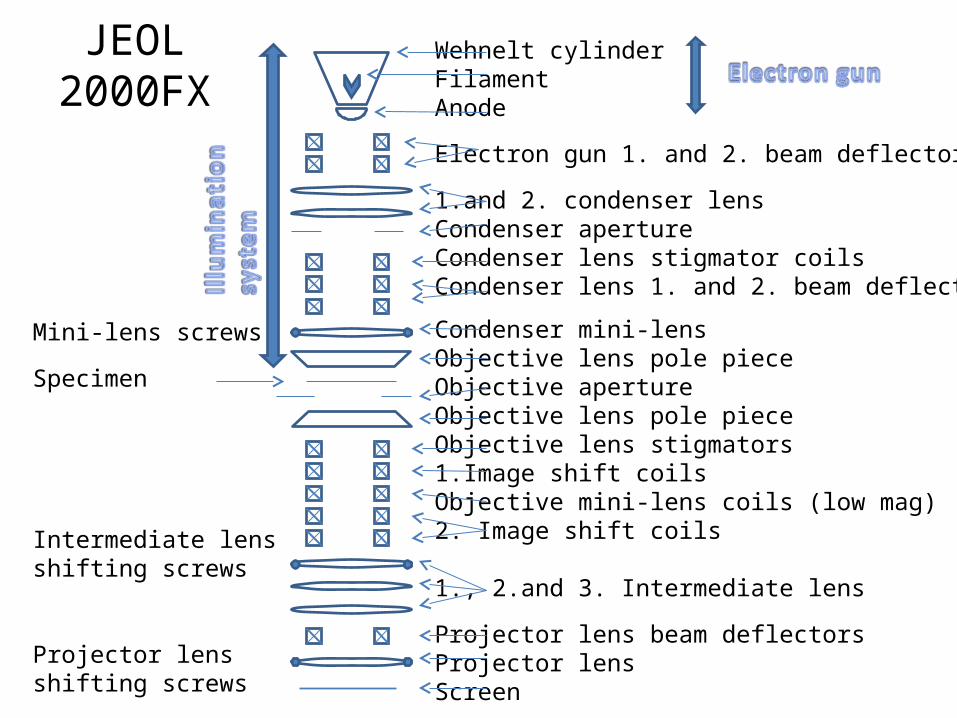
JEOL 2000FX Wehnelt cylinderFilamentAnode
Electron gun 1. and 2. beam deflectors
1.and 2. condenser lensCondenser apertureCondenser lens stigmator coilsCondenser lens 1. and 2. beam deflector
Condenser mini-lensObjective lens pole pieceObjective apertureObjective lens pole pieceObjective lens stigmators1.Image shift coilsObjective mini-lens coils (low mag)2. Image shift coils
1., 2.and 3. Intermediate lens
Projector lens beam deflectorsProjector lensScreen
Mini-lens screws
Specimen
Intermediate lensshifting screws
Projector lensshifting screws


![Ultrafast transmission electron microscopy using a laser ...transmission electron microscopy [4], scanning electron microscopy [5], x-ray diffraction [6], scanning tunneling and atomic](https://static.documents.pub/doc/80x56/607eb1335ce8082131294459/ultrafast-transmission-electron-microscopy-using-a-laser-transmission-electron.jpg)
