Multilayer diffractive optical elements (DOEs) arefrequently exploited in connection to imaging [1]and antireflection coating [2] functions because oftheir unique and programmable spectral properties.It is customary in optics to fabricate spatially homo-geneous layers, whereas alternative layers of poroussilicon (PSi) attract quite a lot of attention as wave-guides [3,4] and Bragg mirrors [5–8] in sensing ap-plications because of their high integrability withmicroelectronics and a large area of contact withsensed chemical analytes. Combinations of dense dif-fraction gratings with layers of PSi have been re-ported in relation to Bragg grating waveguides [3],light coupling to waveguides [4], media for optical re-cording at low incident light power densities [9], andbiomolecular screening with encoded PSi photoniccrystals [10]. However a combination of the PSilayers with DOEs has not been yet reported in litera-ture, to our knowledge.The main motivation for the present study is to ex-
ploit the possibility of a combination of the superbsensing properties of PSi layers with the functionaloptical programmability and high chromatic disper-
sion of DOEs. This paper includes theoretical and ex-perimental parts; the latter carries out some part ofthe issues considered in the theoretical part, in par-ticular, the feasibility proof for the PSi DOEs andmeasurements of their basic performance. The theo-retical part builds novel basic equations for thescalar-diffraction-type reflective surface relief DOEs,which have local grating periods over ten to 20wavelengths and incorporate PSi layers. Genericequations for the depth of the diffractive profile,the diffraction angles, the focal length, and the dif-fraction efficiency as functions of the wavelengthare derived for PSi DOEs. To achieve that, complexrefractive indices of the PSi layers filled with air oranalyte are modeled by the effective index theorycombined with scalar and rigorous diffraction ap-proaches. In particular, we found that the spectralresponse of the PSi DOE may be approximated bythe product of diffraction efficiency of the diffractiveprofile and the reflection coefficient the PSi layer. Toanalyze better an output signal of a generic PSi DOEsensor, a spectral covariance of the diffraction effi-ciency within the entire wavelength range and inseparate spectral bands was defined and theoreti-cally studied, as the criterion for analytes detection.The experimental part reports about fabrication ofPSi binary diffraction gratings and measurementsof their spectral responses at the first diffraction
order, in a device with illuminating and reading fi-bers arranged in the Bragg angle configurations.The theoretical, computer simulation, and experi-mental results are in good agreement and revealthe inherent spectral selectivity of the PSi DOE de-vice at various angular orientations of the readingfiber. The increased spectral selectivity of PSi DOEsopens ways to build vapor and chemical spectrallyaddressed sensors without a dedicated high-resolu-tion spectrometer.
2. Chromatic Properties of Diffractive PorousSilicon Layers
Wavelength-dependent properties of the reflectivesurface relief DOE with the PSi layer are inheritedboth from the DOE diffraction and the reflection ataPSi layer ona silicon (Si)wafer,whicharedependenton the wavelength λ of the incident light. In this sec-tion, we bring together and compare theoretical re-sults of the wavelength-dependent performance forDOEs, PSi layers, and their natural combinations.Figure 1 shows layers of the PSi reflective surface
relief DOE with the staircase blazed microrelief pro-file designed within the scalar diffraction approachfor a given design wavelength λdes and the designeddiffraction order number m. Whereas the diffractiveprofile at Fig. 1 features a constant period typical forthe diffractive prism (blazed diffraction grating), weconsider also a general case of a spatially variablelocal period typical for diffractive lenses and generalDOEs. The layers of the DOE include a planar Si sub-strate, the diffractive microrelief profile on Si, thePSi layer, a planarizing layer, and an ambient med-ium with complex refractive indices nSiðλÞ, nSiðλÞ,nPSiðλÞ, nplanðλÞ, and nincðλÞ, respectively. The planar-izing layer, introduced for generality of our theoreti-cal consideration, has low refractive index nincðλÞ ≤nplanðλÞ < nPSiðλÞ and covers the diffractive profilesuch that the external border to the ambient mediumis planar [11]. A specific case, when the PSi layer isadjacent directly to the ambient medium, withoutany planarizing layer, can formally be treated as aspecial case of the planarizing layer with the refrac-tive index nplanðλÞ ¼ nincðλÞ, coinciding with that ofthe ambient medium.
The staircase diffractive microrelief profile is builtby wrapping the DOE phase function to an interval½0; 2πmÞ and successive quantization to M phasequantization levels. We notice that only the diffrac-tive profile on Si and the planarizing layer have es-sentially variable local thicknesses, whereas thelocal thicknesses for the rest of layers are actuallyuniform and just render the diffractive microreliefprofile. Accordingly, in the reflection mode, the max-imumphase jump 2πmðM − 1Þ=M at the staircasemi-crorelief profile is delivered by the maximum depthof the diffractive profile determined by [12]
and θinc and θout;mðλÞ are the local incident and outputdiffraction angles, shown in Fig. 1.
In cases of the diffractive prism and lens, the dif-fractive change in sine of angle (responsible for thelateral color) and focal length (responsible for theaxial color) vary with wavelength as [1]
nincðλÞ½sin θout;jðλÞ − sin θinc�¼ qjðλÞnincðλdesÞ½sin θout;mðλdesÞ − sin θinc�; ð3Þ
FjðλÞnincðλÞ
¼ 1qjðλÞ
FnincðλdesÞ
; ð4Þ
where j is an arbitrary number of an exploited dif-fraction order, which might be different from thedesigned number m, and
qjðλÞ ¼jλ
mλdes: ð5Þ
Equations (1)–(5), supplemented with nplanðλÞ ¼nincðλÞ, are formally applicable to the specific casewhen the planarizing layer is not present and thePSi layer is adjacent directly to the ambient medium.Figure 2 shows a linear ∝ qjðλÞ change with the illu-mination wavelength λ for the sine of the diffractionangle of the diffractive prism and inverse ∝ ½qjðλÞ�−1change for the focal length of the diffractive lens, incases of blazed M ¼ 8 phase level DOE and binary(M ¼ 2) DOE at different diffraction orders, fornincðλÞ≡ 1 and m ¼ 1. Note that Eqs. (3)–(5) are use-ful for sensing applications and are applicable bothfor the PSi DOE and the regular scalar designedDOE, as the diffraction angle and the focal length
Fig. 1. (Color online) Layer of the PSi reflective surface reliefDOE with the staircase blazed groove profile.
are essentially defined by the spatial structure of dif-fractive zones, which is the same in different layers.In modeling the PSi layer on the Si wafer, we
use data for the refractive index nSi ¼ nSiðλÞ of crys-talline Si in the visible and the near IR range ofwavelengths obtained from in-house ellipsometricmeasurements, which match published data [13]. Auniform thickness PSi layer has pores in Si, whichare filled with air and some possible analyte materialwith the refractive index nanal ¼ nanalðλÞ, partiallydisplacing the air. The porosity (the volume fractionnot filled with silicon to an entire volume of the layer)is p < 1. The volume fraction of the analyte inside thepores is q, which cannot exceed p. As dimensions of Sipores (tenths of nanometers) are small compared tothe wavelength and the angle of incidence is small,the PSi is modeled by the Bruggeman effective med-ium approximation [14], as a homogenous layer witha complex refractive index, satisfying
ð1 − pÞ n2Si − n2
PSi
n2Si þ 2n2
PSiþ q
n2anal − n2
PSi
n2anal þ 2n2
PSi
þ ðp − qÞ n2inc − n2
PSi
n2inc þ 2n2
PSi¼ 0:
ð6Þ
A solution for the complex refractive index arisingfrom Eq. (6) gives the final refractive index nPSi ¼nPSiðλÞ of the PSi layer material as a function ofthe porosity p, the analyte fraction q, and the wave-length λ.Figure 3 shows real (Ren) and imaginary (Imn)
parts of refractive indices for the crystalline Si waferand the uniform PSi layer, having pores with porosityp ¼ 53%, filled either with air only (q ¼ 0) or fullywith water condensate (q ¼ p) considered as an anal-yte (for humidity measurements as an example). It isseen that displacement of the air by the water con-densate inside the pores changes the real part of
the effective refractive index from RenPSi-Air ¼ 2:134to RenPSi-Water ¼ 2:339, whereas crystalline Si hasRenSi ¼ 3:679 (all at λ ¼ λdes ¼ 800nm). Figure 4calculated with software [15] shows wavelength-dependent reflectance coefficients of the bare Siwafer and the uniform PSi layer of thickness hPSi ¼2:12 μm and porosity p ¼ 53% created on the Siwafer. We notice that the graph of the bare Si reflec-tance and its value 32.8% at λ ¼ λdes ¼ 800nm agreewith the data [13], and the graph of the PSi reflec-tance coefficient oscillates with the wavelengthchange, as customary for thin films.
Finally, we considered the PSi diffraction gratingwith PSi pores filled with the air and alternativelywith the water condensate. Figure 5 shows compu-ter-simulated wavelength-dependent diffraction effi-ciency, at−2:75° angle of incidence, in the first order ofthe binary (M ¼ 2, m ¼ 1) PSi diffraction gratingwith the groove depth hmax;2 ¼ 0:2 μm, the periodΛ ¼ 8:5 μm, the duty cycle 0.5, the PSi layer thicknesshPSi ¼ 2:12 μm, and porosity p ¼ 53%. Computersimulations were performed with the DiffractMOD
Fig. 2. (Color online) Ratios qjðλÞ and 1=qjðλÞ for the change insine of the diffraction angle and the focal length, depending on il-lumination wavelength λ, all in cases of the blazed M ¼ 8 phaselevel DOE or the binary (M ¼ 2) DOE in different diffraction or-ders, for the designed diffraction order m ¼ 1 and the designedwavelength λdes ¼ 800nm. At the zero order, the diffraction angleis zero and focus is infinity for any wavelength.
Fig. 3. (Color online) Real (Ren) and imaginary (Imn) parts ofrefractive indices for the crystalline Si wafer and the PSi layerhaving pores with the porosity p ¼ 53%, filled either with air onlyor fully with water condensate as the analyte.
Fig. 4. (Color online) Calculated wavelength-dependent reflec-tance coefficients of the bare Si wafer and the uniform PSi layerof thickness hPSi ¼ 2:12 μm and porosity p ¼ 53% on the Si wafer,modeled with the effective index theory.
software [15], using the rigorous coupled wave ap-proach. Note that respective wavelength-dependentdiffraction angles are defined by Eq. (3). The simula-tion includes the impact of the porosity of the layer onthe effective refractive index and considers the chro-matic dispersion and absorption effects by using thereal and imaginaryparts of refractive indices of theSi,PSi, and water as functions of the wavelength. Thetwo oscillating diffraction efficiency curves refer tothe cases of air orwater in pores.Note that the diffrac-tion efficiency curve in the case of the water in poreshas a different local period and features awavelengthshift relative to the case of air in the pores. The twomonotonic envelope curves provide a reference dif-fraction efficiency of the Si only (without PSi layer)diffraction grating, the lower one of them calculatedrigorously and the upper with the scalar diffractionexpression Eq. (A1) of Appendix A, multiplied overthe wavelength-dependent reflectance of the bareSi wafer.Comparison of the two envelope curves in Fig. 5
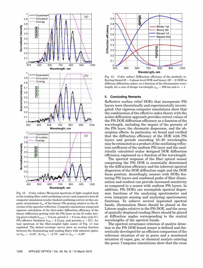
reveals that diffraction calculations within the rigor-ous and scalar diffraction approaches are in agree-ment, as should be for the period-to-wavelengthratio of about 8:5 μm=0:8 μm∼ 10. In addition, wemultiplied the oscillating reflection coefficient (Fig. 4)of the uniform PSi layer by the analytically calcu-lated scalar diffraction efficiency of the binary dif-fraction grating (Fig. 13, case first order, binary)and noticed that the result coincides, at high accu-racy, with the rigorously simulated diffraction effi-ciency of the PSi grating (Fig. 5, oscillating curve,case of air). Therefore, an important result of thissection is that the PSi layer changes the chromaticresponse of the scalar designed DOE, essentiallyby its multiplication over an oscillating thin filmreflection term.
3. Sensors with Porous Silicon DiffractiveOptical Elements
PSi [16] and porous polymer layers are frequentlycalled templates [17] in chemical sensing applica-tions, because they provide a base for building differ-ent sensors with specific responses to different typesof analytes. Porous templates are favorable for che-mical sensing because they have a sponge structureand a very large effective surface area, so they read-ily adsorb analytes. A vapor, gas, or chemical sensorwith the PSi diffraction grating layer may exploitcombined spectral response of the grating and thePSi layer to the incident beam. We propose choosingthe angle of incidence at the PSi gratings as the mthLittrow angle of incidence:
sin θLittrow;m ¼ −mλdes
2nincðλdesÞΛ; ð7Þ
whose sine is half of the sine of the angle between thezero and the mth diffraction orders at the designwavelength λdes, and where Λ is the grating periodand the sign minus indicates an angular orientationof the incident beam at the same side of normal asthe diffractively reflected beam. The beam withλ ¼ λdes, which is incident at the Littrow angle θinc ¼θLittrow;m is diffractively reflected in a directionθout;mðλdesÞ ¼ jθLittrow;mj inverse to its original propa-gation direction and, therefore, demonstrates a kindof retro-reflecting property at the mth diffraction or-der. Sinus of the mth order diffraction angle of thebeam with λ ≠ λdes and θinc ¼ θLittrow;m deviates fromthat of the inverse direction by an amount
∝
� λnincðλÞ
−λdes
nincðλdesÞ�≅
λ − λdesnincðλdesÞ
;
as follows from Eq. (3), applied for λ, j ¼ m and thenfor λ ¼ λdes, j ¼ m.
Figure 6 shows an example of a fiber optical sensorwith the PSi diffraction grating, which comprises clo-sely placed parallel illuminating and reading fiberswith a detector and a beam collimating lens. Angularorientation of the PSi sample is chosen such that themiddle between the fibers subtends the Littrowangle of Eq. (7) with respect to the sample’s normal.Light from the illumination fiber is collimated and
Fig. 5. (Color online) Computer simulated wavelength-depen-dent diffraction efficiency, at −2:75° angle of incidence, in the firstorder of the binary (M ¼ 2, m ¼ 1) PSi diffraction grating withgroove depth hmax;2 ¼ 0:2 μm, period Λ ¼ 8:5 μm, duty cycle 0.5,PSi layer thickness hPSi ¼ 2:12 μm, and porosity p ¼ 53%. The solidand dashed oscillating curves show the cases of PSi pores filledwith air and water, respectively.
Fig. 6. (Color online) Fiber optical sensor with the PSi diffractiongrating and the collimating lens.
then diffractively reflected at the PSi grating, at thewavelength-dependent diffraction angle and effi-ciency, as depicted by the graphs of the first diffrac-tion order in Figs. 2 and 5. The reflected light isfocused by the collimating lens, such that the focalpoint at λ ¼ λdes is located exactly on the core ofthe reading fiber. Focal spots of various wavelengthsare diffractively shifted. At wavelengths adjacent tothe design wavelength λ ¼ λdes the focal spots par-tially overlap with the core area of the reading fiberwhereas, at other wavelengths, they miss it. To com-pare, the uniform PSi layer specularly reflects lightof all wavelengths to a fixed reading fiber positionthat is independent of the wavelength. Accordingly,the spectral selectivity of the sensor with the diffrac-tively structured PSi layer is higher, compared to thesensor with the uniform PSi layer. The sensor addi-tionally equipped with several reading fibers placedat different spatial positions will naturally access dif-fraction angles at several wavelengths and provideparallel signals in several respective spectral bandsof the light. The sensor may be equipped also withseveral illuminating fibers placed at different spatialpositions to provide extra light power and severalspectral maxima. Such a multispectral arrangementmay assist in discrimination between different anal-ytes having specific behavior of their spectral signa-tures in appropriate spectral bands.Figure 7 shows a further example of the fiber
optical sensor that exploits the PSi diffractive lens,serving both as a dispersive sensing element and afocusing lens. The core of the illumination fiber isimaged, at the design wavelength λdes, onto the coreof the reading fiber. The spectral selectivity here isfurther increased, compared with the uniform PSilayer and even with the PSi grating of Fig. 6. Thecause is that the light at wavelengths λ different fromλdes deviates from the reading fiber core both in angleand, subsequently, in focus position, as determinedby the curves of the graphs corresponding to the firstdiffraction order in Fig. 2. In this optical scheme, thePSi DOE sensor may involve the linear fiber array orthe light detector array in place of the single readingfiber and, optionally, an array of illuminating fibers,to measure several readings of diffraction efficiencyandmake the PSi DOE sensor itself serve as a simplelow-resolution spectrometer.When the PSi DOE sensor operates, vapors of the
analyte molecules may penetrate into the sponge
structure of the PSi layer, displace the air, and con-dense into the liquid phase, thus changing the refrac-tive index and absorption in the pores. The DOEswith the PSi layers respond to that with a changeddependence of diffraction efficiency on the wave-length, as illustrated in Fig. 5 for the case of watercondensate. The spectral response of the sensor isclosely related to the diffraction efficiency as a func-tion of the wavelength. To have efficient means forcomparison between the wavelength-dependent dif-fraction efficiency ηairðλÞ in the initial situation ofair in pores and the changed diffraction efficiencyηanalyteðλÞ at the analyte exposed situation, we pro-pose in this paper to use a normalized spectralcovariance criterion for the diffraction efficiencyfunction. Such a criterion is defined as
rðΔλÞ ¼ CðΔλÞCð0Þ ;
CðΔλÞ ¼Zλmax
λmin
½ηairðλþΔλÞ − �ηair�½ηanalyteðλÞ
− �ηanalyte�dλ;
ð8Þ
where λmin, λmax define the limits of the wavelengthband of interest and values of ηair and ηanalyte are setas zeros out of the band,
�ηair ¼1
λmax − λmin
Zλmax
λmin
ηairðλÞdλ;
�ηanalyte ¼1
λmax − λmin
Zλmax
λmin
ηanalyteðλÞdλ; ð9Þ
and Δλ is the wavelength shift for the covariance.Obviously jrðΔλÞj ≤ 1.
Figure 8 shows the computer simulated spectralcovariance rðΔλÞ of the diffraction efficiency of thebinary (M ¼ 2, m ¼ 1) diffraction grating versusthe wavelength shift Δλ for an entire wavelengthrange of 400–1000nm and separately in three spec-tral bands: band 1, 523–682nm; band 2, 681–840nm;and band 3, 841–1000nm. The binary diffractiongrating has groove depth hmax;2 ¼ 0:2 μm, periodΛ ¼ 8:5 μm, duty cycle 0.5, PSi layer thicknesshPSi ¼ 2:12 μm, porosity p ¼ 53%, and it performsat angle of incidence −2:75°. Attributing to severalspectral bands models the PSi DOE sensor withthe array of spatially displaced reading fibers, suchthat each fiber is installed at a different Littrow an-gle corresponding to the central wavelength of thespectral band.
Specifically, Fig. 8(a) shows the autocovariance inthe reference case when the PSi pores are entirelyfilled with air and Fig. 8(b) shows the cross covar-iance of the diffraction efficiency between the casewhen the PSi pores are filled with water condensate
Fig. 7. (Color online) Fiber optical sensor with the PSi diffractivelens, which serves both as the dispersive sensing element and thefocusing lens.
and the reference case. As is well known, the autoco-variance integral is symmetrical and has a peak inthe center, as shown in Fig. 8(a). In contrast, thecross covariance integral is asymmetrical and doesnot have a peak in the center. The cause of the asym-metry is the displacement of air by water in the poresof the PSi layer. Therefore, the asymmetry of the co-variance of Eq. (8), between the reference and theanalyte cases, may serve as the efficient criterionfor the chemical sensor with the PSi DOE. In addi-tion, several separate spectral bands can assist indiscrimination among different analytes.
4. Fabrication and Experimentation with PorousSilicon Diffractive Optical Elements
This section is dedicated to experimental issues, witha goal of showing the feasibility of the PSi DOEs andillustrating their basic performance. The PSi DOEsfabrication technology brings together technologiesdeveloped for DOEs and for uniform PSi layers.
Uniform PSi layers are routinely produced by theelectrochemical dissolution of crystalline silicon in ahydrofluoric acid (HF) and ethanol based electrolyte,wherein the crystalline silicon sample serves as theanode and a platinum electrode serves as the cathode[7]. The resulting structure consists of pores ran-domly alternating with crystalline silicon rodsattached to the crystalline silicon substrate. Thethickness of the PSi layer and its porosity can be con-trolled by the process time and the electric currentdensity level in a given crystalline silicon wafer,and the proportion of HF in the electrolyte solution[5]. Diffraction gratings and DOEs with PSi layerscan be produced by a combination of the electroche-mical process with either interferometric lithogra-phy, ion implantation [4], laser micromachining [3,9],or photolithography [10].
For fabrication of the PSi DOE, we have chosenphotolithographic fabrication of the Si DOE on theSi wafer followed by the electrochemical processfor forming the uniform PSi layer that renders thediffractive microrelief profile. In more detail, inour fabrication process of binary scalar-diffraction-type PSi diffraction gratings, we started with20mm × 20mm Si samples prepared by dicing of apþ doped bulk 600 μm thick crystalline silicon wafer,with resistivity of 0:01–0:02Ω cm, purchased fromWaferNet Inc. The sample was lithographically ex-posed to UV light in themask aligner via a chromiummask having straight lines with a period of Λ ¼8:5 μmand a duty cycle of 0.7. Successive dry reactiveion etching down to the monitored depth of hmax;2 ¼0:2 μm yielded an intermediate crystalline Si binarydiffraction grating providing the phase difference of πat the design wavelength λdes ¼ 800nm, for small an-gles of incidence in the reflection mode. Then thesample was electrochemically etched by a stable cur-rent density of 25mA=cm2 for 200 s in an electrolytesolution containing 15% HF acid in ethanol, to formthe PSi layer above diffractive grooves and gaps. Wealso rinsed the sample with ethanol and pentane.The PSi layer had thickness hPSi ¼ 2:70 μm and por-osity p ¼ 53%, estimated in accordance with the lit-erature process data [18]. Figure 9 shows scanningelectron microscopy (SEM) pictures, in top views[Figs. 9(a) and 9(b)] and in cross section [Figs. 9(c)and 9(d)], of the binary diffraction grating with thePSi layer having porosity p ¼ 53% and thicknesshPSi ¼ 2:70 μm. Figure 9 reveals that the PSi layerscreated feature nearly uniform thickness, renderingthe diffractive microrelief profile at different diffrac-tive zones.
The fabricated PSi diffraction grating was opti-cally investigated in an experimental arrangement
Fig. 8. (Color online) Computer-simulated spectral covariancerðΔλÞ of the diffraction efficiency of the binary (M ¼ 2, m ¼ 1) dif-fraction grating versus the wavelength shift Δλ, for an entirewavelength range 400–1000nm and separately in three spectralbands: band 1, 523–682nm; band 2, 681–840nm; and band 3,841–1000nm. The groove depth is hmax;2 ¼ 0:2 μm, the period isΛ ¼ 8:5 μm, the duty cycle is 0.5, the PSi layer thickness ishPSi ¼ 2:12 μm, the porosity is p ¼ 53%, and the angle of incidenceis −2:75°. (a) Autocovariance in a case when the PSi pores are filledwith air and (b) cross covariance between cases when PSi pores arefilled with air or water. Notice an asymmetry in the cross covar-iance appearing with condensation of water in the pores of thePSi layer.
shown in Fig. 10, where a fiber-coupled tungstenhalogen lamp (Ocean Optics LS-1) was coupled toa bundle of six illumination 400 μm fibers, surround-ing a central 400 μm reading fiber attached to a spec-trometer (Ocean Optics USB4000). The seven fiberswere packaged by the manufacturer into a bundlecoupled into a collimating lens to transform the out-going radiation into a nearly parallel beam and focusthe reflected light from the PSi grating back to thecore of the reading fiber. The measured spectrumof the fiber-coupled light source is shown in Fig. 11.The reflecting sample of the PSi binary grating wasangular oriented in accordance with the Littrow an-gle as given by Eq. (7), m ¼ 1. The spectrum of thereflected light was monitored in the wavelengthrange from 400 to 1000nm.Figure 12 shows the measured spectrum of light
coupled back to the reading fiber after reflection fromthe PSi grating (solid oscillating curves) and respec-tive best-fit computer simulation results (dashed os-cillating curves) at thee angular orientations of the
PSi grating at −2:30°, −2:75°, and −3:20° relativeto the direction of the specular reflection. Note thatthe Littrow angle for the design wavelength λdes ¼800nm is θLittrow;1 ¼ −2:70°. We applied a commonnormalization for the entire set of thee angular orien-tations. The computer simulation comprised rigorouscalculation of the first-order diffraction efficiency ofthe binary diffraction grating with PSi layers onthe Si wafer, having groove depth hmax;2 ¼ 0:2 μm,period Λ ¼ 8:5 μm, and a duty cycle of 0.7. The effec-tive thickness of the PSi layer with porosity p ¼ 53%in the simulations was chosen to be hPSi ¼ 2:12 μm asproviding a best fit to the period and the location ofthe local maxima of the oscillating spectral curves inthe theory to those in the experiment. A correctionfor the actual light source spectrum (Fig. 11) andan estimated “overlap function” between the illumi-nating and reading fibers with inherent optics wereapplied to the simulation data. The overlap functionwas modeled as the overlap area between two differ-ent circles whose parameters were estimated by thebest fit of experimental and computer simulateddata. The overlap function shifts its position withinthe wavelength spectrum with the change of the an-gular orientations of the PSi grating, as shown by thedotted envelope curves in Fig. 12. Figures 12(a)–12(c)reveal good agreement between experimental andthe best-fit computer simulated data. Also revealedis an envelope shift of themeasured spectrum of lightby about 75nm for each 0:45° change in the angularorientation of the PSi grating. Such an envelope shiftcan be explained by missing of the reading fiber coreby the light of some wavelengths, because of spectraldispersion of the first-order diffraction angle in thePSi grating sensor. This provides an experimentalproof for the expected increase in the spectral selec-tivity of the PSi grating sensor as compared to theuniform PSi sensor, where the reflected light ofall wavelengths arrives to the fixed reading fiberposition.
Fig. 9. SEM pictures of the binary PSi diffraction grating withthe groove depth hmax;2 ¼ 0:2 μm, period Λ ¼ 8:5 μm, duty cycle0.7, porosity p ¼ 53%, and thickness hPSi ¼ 2:70 μm. (a) Top view,magnification ×4500; (b) top view,magnification ×100; 000; (c) crosssection, magnification ×9500; and (d) cross section, magnification×23; 000.
Fig. 10. (Color online) Optical arrangement of the experimentwith the fiber optical sensor based on the PSi diffraction grating.
Fig. 11. (Color online) Spectrum of the fiber-coupled light sourcemeasured in the experiment.
Reflective surface relief DOEs that incorporate PSilayers were theoretically and experimentally investi-gated. Our rigorous computer simulations show thatthe combination of the effective index theory with thescalar-diffraction approach provides correct values ofthe PSi DOE diffraction efficiency as a function of thewavelength, including the impact of the porosity ofthe PSi layer, the chromatic dispersion, and the ab-sorption effects. In particular, we found and verifiedthat the diffraction efficiency of the DOE with PSilayers and periods exceeding 10–20 wavelengthsmay be estimated as aproduct of the oscillating reflec-tion coefficient of the uniform PSi layer and the anal-ytically calculated scalar designed DOE diffractionefficiency, expressed as a function of the wavelength.
The spectral response of the fiber optical sensorcomprising the PSi DOE is essentially determinedby the diffraction efficiency and the inherent spectraldispersion of the DOE diffraction angle and the DOEfocus position. Accordingly, sensors with DOEs fea-turing PSi layers and combined paths of fiber illumi-nation and readout can provide increased sensitivityas compared to a sensor with uniform PSi layers. Inaddition, PSi DOEs can accomplish spectral disper-sion functions of the analyzing spectrometer andeven integrate sensing and analyzing spectrometerfunctions. To achieve several separated spectralbands, illumination fibers should be placed at theLittrow angles relative to the PSi DOE, and the arrayof spatially displaced reading fibers should be placedat diffraction angles corresponding to the centralwavelengths of the spectral bands.
The spectral covariance criterion of analyte detec-tion in the PSi DOE-based sensor is defined and the-oretically developed for an efficient comparison of thereference situation of air in pores and a monitoredsituation of vapor, gas, or chemical analyte enteringthe pores. Computer simulations show that the cross
Fig. 12. (Color online) Measured spectrum of light coupled backto the reading fiber (solid oscillating curves) and respective best-fitcomputer simulation results (dashed oscillating curves) at thee an-gular orientations θinc of the binary PSi grating relative to the di-rection of the specular reflection. Computer simulations comprisedrigorous calculation of the first-order diffraction efficiency of thebinary diffraction grating with the PSi layer on the Si wafer, hav-ing groove depth hmax;2 ¼ 0:2 μm, periodΛ ¼ 8:5 μm, duty cycle 0.7,PSi effective thickness hPSi ¼ 2:12 μm, and porosity p ¼ 53%. Ac-tual spectrum of the fiber-coupled light source of Fig. 11 wasexploited. The dotted envelope curves show an overlap functionbetween the illuminating and reading fibers with inherent optics.(a) θinc ¼ −2:30°, (b) θinc ¼ −2:75°, and (c) θinc ¼ −3:20°.
Fig. 13. (Color online) Diffraction efficiency of the perfectly re-flecting blazedM ¼ 8 phase level DOE and binary (M ¼ 2) DOE indifferent diffraction orders, as a function of the illumination wave-length, for a case of design wavelength λdes ¼ 800nm and m ¼ 1.
covariance for thediffractionefficiencyasa function ofthe wavelength, at several separated spectral bands,displays asymmetry when the analyte enters thepores.The fabrication and the experimental investigation
of the PSi binary diffraction grating with a period of8:5 μm substantiate the feasibility of PSi DOEs andshow good agreement between the experimentallymeasured and computer-simulated spectral responseof the fiber optical sensor comprising the PSi DOE.The basic understanding of the main optical prop-
erties of DOEs comprising PSi layers achieved in thispaper opens ways to develop vapor and chemical sen-sors and other devices exploiting PSi DOEs.
Appendix A. Scalar of a Reflective Diffractive OpticalElement
The outcome of this appendix is used for the scalardiffraction efficiency calculations in Fig. 5, refer-enced at the end of Section 2.Let us consider a DOE with the maximum diffrac-
tive profile depth of hmax;M per Eq. (1), designed fordiffraction ordernumberm, without aPSi layer.A sca-lar diffraction estimation of the diffraction efficiencyin an arbitrary jth diffraction order a given angle ofincidence may be derived from equations [1,12] as
ηjðλÞ ¼ sinc2�
jM
�sinc2½jcontðλÞ − j�sinc2
�jcontðλÞ−j
M
� ; ðA1Þ
where
jcontðλÞ ¼ mcðλÞ; cðλÞ ¼ λdesλ
μjðλÞμmðλdesÞ
;
and μjðλÞ is defined by Eq. (2). We notice that the dif-fraction efficiency in the case of the reflection DOEessentially depends on the wavelength ratio, stillweakly depending on angles and refractive indices.The DOE provides maximum scalar diffraction ef-
ficiency at the design wavelength λdes and reducedscalar diffraction efficiency at wavelengths λ, differ-ent from λdes, as seen from Eq. (A1). The diffractionefficiency per Eq. (A1) also reaches local maxima at adiscrete set of wavelengths λ, providing an integervalue jopt to the function jcontðλÞ. Figure 13 showsthe scalar diffraction efficiency of a perfectly reflect-ing blazed staircaseM ¼ 8 phase level DOE and bin-ary (M ¼ 2), perfectly reflecting the DOE in differentdiffraction orders, as a function of the illuminationwavelength λ. At the design wavelength λ ¼λdes ¼ 800nm, the diffraction efficiency of the firstdiffraction order reaches its maximum of 95% forM ¼ 8 phase levels and 40.5% for binary M ¼ 2 levelDOEs.
The authors acknowledge the assistance of DaniHak in providing us with the results of his ellipso-
metric measurements and the software for calcula-tion of the effective refractive index of uniform PSilayers. The authors acknowledge support of the Min-istry of Science of Israel.
References1. D. Faklis and G. M. Morris, “Spectral properties of multiorder
diffractive lenses,” Appl. Opt. 34, 2462–2468 (1995).2. U. Schulz, “Wideband antireflection coatings by combining
interference multilayers with structured top layers,” Opt.Express 17, 8704–8708 (2009).
3. I. Reaa, M. Iodicea, G. Coppolaa, I. Rendinaa, A. Marinob, andL. De Stefano, “A porous silicon-based Bragg grating wave-guide sensor for chemical monitoring,” Sens. Actuators B139, 39–43 (2009).
4. N. Nagy, J. Volk, A. Hámori, and I. Bársony, “Submicrometerperiod silicon diffraction gratings by porous etching,” Phys.Status Solidi A 202, 1639–1643 (2005).
5. L. De Stefano, I. Rendina, L. Moretti, S. Tundo, and A. M.Rossi, “Smart optical sensors for chemical substances basedon porous silicon technology,” Appl. Opt. 43, 167–172(2004).
6. T. Jalkanen, V. Torres-Costa, J. Salonen, M. Björkqvist,E. Mäkilä, J. M. Martínez-Duart, and V.-P. Lehto, “Opticalgas sensing properties of thermally hydrocarbonized poroussilicon Bragg reflectors,” Opt. Express 17, 5446–5456(2009).
7. M. G. Bergers, C. Dieker, M. Thonissen, L. Vescan, H. Luth, H.Muender, W. Theiss, M. Wernke, and P. Grosse, “Porositysuperlattices: a new class of Si heterostructures,” J. Phys. D27, 1333–1336 (1994).
8. P. A. Snow, E. K. Squire, P. J. St. Russel, and L. T. Canham,“Vapor sensing using the optical properties of porous siliconBragg mirrors,” J. Appl. Phys. 86, 1781–1784, (1999).
9. A. Alexeev-Popov, S. Gevelyuk, Ya. Roizin, and D. Savin, “Dif-fraction gratings on porous silicon,” Solid State Commun. 97,591–593 (1996).
10. F. Cunin, T. A. Schmedake, J. R. Link, Y. Y. Li, J. Koh, S. N.Bhatia, and M. J. Sailor, “Biomolecular screening withencoded porous-silicon photonic crystals,” Nat. Mater. 1, 39–41 (2002).
11. D. Chambers, G. Nordin, and S. Kim, “Fabrication andanalysis of a three-layer stratified volume diffractive opticalelement high-efficiency grating,” Opt. Express 11, 27–38(2003).
12. M. A. Golub, “Generalized conversion from the phase functionto the blazed surface-relief profile of diffractive optical ele-ments,” J. Opt. Soc. Am. A 16, 1194–1201 (1999).
13. Properties of Silicon, Vol. 4 of European MathematicalInformation Service (EMIS) Datareview Series (INSPEC/IEE, 1988).
14. C. F. Bohren and D. R. Huffman, The Absorption andScattering of Light By Small Particles (Wiley, 1983),p. 217.
15. DiffractMOD software code, Rsoft Design Group Inc., www.rsoftdesign.com.
16. R. Herino, G. Bomchil, K. Barla, C. Bertrand, and J. L. Ginoux,“Porosity and pore size distributions of porous silicon layers,”J. Electrochem. Soc. 134, 1994–2000 (1987).
17. S. J. Kim, V. P. Chodavarapu, A. N. Cartwright, M. T. Swihart,and T. J. Bunning, “Enhanced oxygen detection using porouspolymeric gratings with integrated recognition elements,”Sens. Actuators B 130, 758–764 (2008).
18. C. Mazzoleni and L. Pavesi, “Application to optical compo-nents of dielectric porous silicon multilayers,” Appl. Phys.Lett. 67, 2983 (1995).