187
DIFFRACTIVE OPTICS NEAR-FIELD LASER LITHOGRAPHY FOR FABRICATION
OF 3-DIMENSIONAL PERIODIC NANOSTRUCTURES
by
Debashis Chanda
A thesis submitted in conformity with the requirements
for the degree of Doctorate of Philosophy
Graduate Department of Electrical and Computer Engineering
University of Toronto
©Copyright by Debashis Chanda, 2009

Abstract
Di�ractive optics near-�eld laser lithography for fabrication of 3-dimensional periodicnanostructures
Debashis Chanda
Doctorate of Philosophy
Graduate Department of Electrical and Computer Engineering
University of Toronto
2009
The main objective of the present research work is to fabricate three dimensional photonic
nanostructures in photo-sensitive polymers using a novel di�ractive optical element (DOE)
based lithography technique. A di�ractive optical element is a promising alternative device
for 3D fabrication where one DOE creates multiple laser beams in various di�raction or-
ders that are inherently phase-locked and stable for reproducible creation of 3D near-�eld
di�raction patterns from a single laser beam. These near-�eld patterns are captured in-
side a photosensitive material like photoresist to fabricate 3D photonic crystal templates.
We have demonstrated fabrication of a wide range of 3D structures having di�erent crystal
symmetries and di�erent relative crystal axis ratios. The present work has provided 3D
photonic crystal nanostructures with uniform optical and structural properties over large
sample area (∼3-4 mm diameter) and through large 15-50 µm thickness with large number
of layers (> 40) having period 550 nm - 650 nm and feature sizes between 200 nm and 300
nm. The short exposure time and small number of process steps shows promise for scaling
to very large volume fabrication, dramatically improving the throughput, quality and struc-
tural uniformity of 3D periodic nanostructures, especially over that provided by tedious and
ii

costly semiconductor processing technology. The di�ractive optics lithography is a paral-
lel processing method that is easily scalable to generate centimeter-scale 3D nanostructures
having large number of layers in several seconds. Due to low refractive index contrasts these
polymer templates possess partial stopgaps along several crystallographic directions which
can be practically used in several device or sensor applications where complete bandgap is
not necessary. The potential usefulness of these partial stopbands for refractive index sens-
ing of liquids has been demonstrated. These low refractive index polymer structures have
been inverted with amorphous silica to convert a �soft� polymer structure to a robust �hard�
structure. Further, few preliminary tests were done in fabricating 3D nanostructures into
micro-�uidic channels for potential chromatography applications. The practical merits of
this 3D fabrication technique will enable new practical manufacturing methods for optical
and MEMS applications of 3D micro and nano structures.
iii

Acknowledgments
Starting a PhD was like looking for someone in a big city without knowing his address. Atthe beginning it was felt like a never ending endeavor. However, the journey was memorablefor a adventurous person like me which surely made me a better person. In that four yearsprocess, many people helped me in various capacity. The prime contribution came frommy wife Kakoli. She relentlessly worked to support me �nancially without any complain.I couldn't give her much time due to my strict 10 am to 10 pm daily work schedule. Theproblem became severe during her pregnancy when she had to remain alone till late night athome. Each day she used to urge me to come back early and I had to make false promisesdue to my late night SEM bookings. I hope this will not happen ever in my life. The biggestjoy of our life came with the advent of our daughter Ishani. Looking at her calm and angelicface I used to forget my research anxiety. The little one immensely helped me during myboring thesis writing phase by providing constant entertainments in her own ways.
I thank Dr. Alongkarn Chutinan for all his guidance and help. He always had enoughtime for me for any discussion. I should thank Ladan for fabricating a multi-level di�ractiveoptical element using femtosecond direct laser writing. This was a very good collaborationbetween both of us. Moez did an excellent work in converting my Matlab based photonicband calculation code to a highly e�cient C-code. He also worked with me in various aspectsof photonic crystal modeling. I appreciate Nicole for helping me in template inversion process.I thank Sergey, who was an important person in my PhD work. He was a key person inbuilding up the Argon Ion laser lab and improving my experimental setup. I thank Shane forassisting me at various times during my PhD from computer related help to thesis formatinghelp. He was the 'go-to-man' during my PhD in our group. I thank Haibin for trainingme on Argon Ion laser and �ber Bragg grating writing. I am grateful to Mi Li for doinghigh quality AFM for me. I thank Leon for carrying on my research. I appreciate Abbasfor his time and e�ort to make laser drilled apertures on thin aluminum foil for me. Iam thankful to Tariq for his many computer related help. I thank Prof. Amr Helmy forhis constant encouragement. Although Dr. Li, Amir, Stephen, Rajeev, Alam, Jason andValeria were not involved in my research, it was a pleasure having them as my colleagues.Most importantly, I thank my supervisor Peter Herman, for his constant encouragementand guidance. Peter always pushed me to strive harder in my research and improve mygraphical representation skills. I am grateful to Peter for supporting me to attend manyinternational conferences which gave me the opportunity to present my work in front of thescienti�c community and meet other experts in my �eld. I am grateful for support from theUniversity of Toronto Scholarship, Ontario Graduate Science and Technology Scholarship(OGSST), Ontario Graduate Scholarship (OGS).
I am grateful to my family for providing me all kinds of support since my childhood. Iappreciate my in-laws for their encouragement and patience. I thank my father for tellingme stories of many scientists and their inventions throughout my childhood which immenselymotivated me for scienti�c explorations. I am grateful to Boroma and Jatha for their endlesslove and pampering. My life has little meaning without my mother. I owe all my virtuesto her. Sadly, I can't tell you the story of my journey. However, I can see your proud andhappy face among bright stars in the sky.
iv

Contents
Acknowledgements iv
Published Work xxiv
List of Acronyms xxvii
1 Introduction 1
1.1 Motivation . . . . . . . . . . . . . . . . . . . . . . . . . . . . . . . . . . . . . 2
1.2 New contributions . . . . . . . . . . . . . . . . . . . . . . . . . . . . . . . . . 4
1.3 Overview of the dissertation . . . . . . . . . . . . . . . . . . . . . . . . . . . 6
2 Background on three-dimensional periodic structures 9
2.1 Brief history of photonic bandgap concept . . . . . . . . . . . . . . . . . . . 9
2.2 Bandgap theory . . . . . . . . . . . . . . . . . . . . . . . . . . . . . . . . . . 11
2.3 Three-dimensional periodic structures of special interest . . . . . . . . . . . . 14
2.3.1 Diamond structure . . . . . . . . . . . . . . . . . . . . . . . . . . . . 15
2.3.2 Diamond-like structure . . . . . . . . . . . . . . . . . . . . . . . . . . 16
2.4 Nano fabrication of 3D periodic structures . . . . . . . . . . . . . . . . . . . 17
2.4.1 Semiconductor lithography . . . . . . . . . . . . . . . . . . . . . . . . 17
2.4.2 Self-assembly . . . . . . . . . . . . . . . . . . . . . . . . . . . . . . . 19
2.4.3 Direct laser writing . . . . . . . . . . . . . . . . . . . . . . . . . . . . 20
2.4.4 Holographic lithography . . . . . . . . . . . . . . . . . . . . . . . . . 22
v

2.5 Limitations of present 3D fabrication techniques . . . . . . . . . . . . . . . . 23
3 Three-dimensional di�ractive optics lithography 27
3.1 Introduction . . . . . . . . . . . . . . . . . . . . . . . . . . . . . . . . . . . . 27
3.2 Talbot self-imaging . . . . . . . . . . . . . . . . . . . . . . . . . . . . . . . . 28
3.3 Arranging Talbot self-images into a photonic crystal . . . . . . . . . . . . . . 29
3.3.1 One-dimensional vs. two-dimensional di�ractive elements . . . . . . 30
3.3.2 De�ning lattice constants . . . . . . . . . . . . . . . . . . . . . . . . 30
3.4 Determining depth of near-�eld . . . . . . . . . . . . . . . . . . . . . . . . . 33
3.5 Simulation of near-�eld intensity distribution . . . . . . . . . . . . . . . . . 36
3.5.1 Di�raction e�ciency calculation . . . . . . . . . . . . . . . . . . . . 37
3.5.2 Isointensity calculation . . . . . . . . . . . . . . . . . . . . . . . . . 38
3.5.2.1 Interference equation based beam re-combination method . 39
3.5.2.2 Finite di�erence time domain method . . . . . . . . . . . . 40
3.6 Controlling near-�eld intensity distribution . . . . . . . . . . . . . . . . . . 41
3.6.1 E�ect of di�raction e�ciency . . . . . . . . . . . . . . . . . . . . . . 41
3.6.2 E�ect of polarization . . . . . . . . . . . . . . . . . . . . . . . . . . . 43
3.6.2.1 E�ect on di�raction e�ciency and intensity contrast . . . . 43
3.6.2.2 E�ect on motif shape . . . . . . . . . . . . . . . . . . . . . . 45
3.6.3 E�ect of relative phase of di�racted beams . . . . . . . . . . . . . . . 48
3.7 Photonic band calculation . . . . . . . . . . . . . . . . . . . . . . . . . . . . 49
3.7.1 Plane wave expansion theory . . . . . . . . . . . . . . . . . . . . . . 50
3.7.2 Numerical plane wave expansion of periodic structures . . . . . . . . 51
vi
3.7.2.1 Discrete representation and classi�cation of the 3D periodic
structures . . . . . . . . . . . . . . . . . . . . . . . . . . . . 52
3.7.2.2 Numerical representation of plane wave expansion . . . . . . 52
3.7.3 Band calculation of 3D periodic structures . . . . . . . . . . . . . . . 56
3.7.3.1 Dependence of band calculation on number of plane waves . 58
3.7.3.2 Dependence of band calculation on sampling frequency . . . 60
3.8 Summary . . . . . . . . . . . . . . . . . . . . . . . . . . . . . . . . . . . . . 61
4 Di�ractive optics for fabrication of diamond-like structures 63
4.1 Introduction . . . . . . . . . . . . . . . . . . . . . . . . . . . . . . . . . . . . 63
4.2 Diamond-like woodpile structure . . . . . . . . . . . . . . . . . . . . . . . . . 64
4.3 Bandgap optimization of woodpile structure . . . . . . . . . . . . . . . . . . 65
4.3.1 Complete bandgap . . . . . . . . . . . . . . . . . . . . . . . . . . . . 65
4.3.2 Optimized DOE parameters . . . . . . . . . . . . . . . . . . . . . . . 66
4.4 Di�ractive optics for diamond-like structure . . . . . . . . . . . . . . . . . . 69
4.4.1 One-dimensional DOE based double laser exposure method . . . . . 70
4.4.1.1 One-dimensional phasemask design . . . . . . . . . . . . . . 70
4.4.1.2 Interlacing of two orthogonally rotated interference patterns 72
4.4.2 Phase tunable DOE for single exposure method . . . . . . . . . . . . 74
4.4.2.1 Phase tunable DOE . . . . . . . . . . . . . . . . . . . . . . 74
4.4.2.2 Phase control principles . . . . . . . . . . . . . . . . . . . . 75
4.4.2.3 Finite di�erence time domain predictions of phase tunable
near-�eld di�raction pattern . . . . . . . . . . . . . . . . . . 78
4.4.3 Multi-level 2D DOE for single exposure method . . . . . . . . . . . . 79
vii
4.4.3.1 Two-level vs. proposed three-level 2D DOE . . . . . . . . . 80
4.4.3.2 Working principles of three-level DOE . . . . . . . . . . . . 81
4.4.3.3 Three-level DOE design . . . . . . . . . . . . . . . . . . . . 82
4.4.3.4 Finite di�erence time domain predictions of near-�eld di�rac-
tion pattern . . . . . . . . . . . . . . . . . . . . . . . . . . . 85
4.5 Summary . . . . . . . . . . . . . . . . . . . . . . . . . . . . . . . . . . . . . 88
5 Experimental 89
5.1 Experimental . . . . . . . . . . . . . . . . . . . . . . . . . . . . . . . . . . . 89
5.1.1 Laser system . . . . . . . . . . . . . . . . . . . . . . . . . . . . . . . 89
5.1.1.1 Beam delivery system . . . . . . . . . . . . . . . . . . . . . 90
5.1.1.2 Beam pro�le . . . . . . . . . . . . . . . . . . . . . . . . . . 91
5.1.2 Sample preparation . . . . . . . . . . . . . . . . . . . . . . . . . . . 92
5.1.3 Post exposure baking and development . . . . . . . . . . . . . . . . . 93
5.1.4 Characterization . . . . . . . . . . . . . . . . . . . . . . . . . . . . . 94
5.1.4.1 Structural characterization . . . . . . . . . . . . . . . . . . 94
5.1.4.2 Optical characterization . . . . . . . . . . . . . . . . . . . . 95
6 Fabrication using one-dimensional di�ractive optics 97
6.1 Introduction . . . . . . . . . . . . . . . . . . . . . . . . . . . . . . . . . . . . 97
6.2 One-dimensional DOE for double laser exposure method . . . . . . . . . . . 98
6.2.1 Laser exposure setup . . . . . . . . . . . . . . . . . . . . . . . . . . . 98
6.2.2 Fabrication of 3D woodpile structures . . . . . . . . . . . . . . . . . 99
6.3 Phase tunable DOE for single exposure method . . . . . . . . . . . . . . . . 102
6.3.1 Laser exposure setup . . . . . . . . . . . . . . . . . . . . . . . . . . . 102
viii

6.3.2 Woodpile structure with TTR symmetry . . . . . . . . . . . . . . . . 103
6.3.3 Structure with BCT symmetry . . . . . . . . . . . . . . . . . . . . . 104
6.3.4 Fabrication of diamond-like structure with circularly polarized light . 105
6.4 Optical characterization . . . . . . . . . . . . . . . . . . . . . . . . . . . . . 107
6.4.1 Near-infrared characterization . . . . . . . . . . . . . . . . . . . . . . 107
6.4.2 Telecom-band characterization . . . . . . . . . . . . . . . . . . . . . . 109
6.5 Discussion . . . . . . . . . . . . . . . . . . . . . . . . . . . . . . . . . . . . . 111
7 Fabrication using two-dimensional di�ractive optics 113
7.1 Introduction . . . . . . . . . . . . . . . . . . . . . . . . . . . . . . . . . . . 113
7.2 Fabrication of two-dimensional di�ractive optics . . . . . . . . . . . . . . . . 114
7.2.1 Two-level DOE . . . . . . . . . . . . . . . . . . . . . . . . . . . . . . 115
7.2.2 Three-level DOE fabrication by two photon polymerization . . . . . . 115
7.3 Single exposure fabrication of 3D photonic crystals . . . . . . . . . . . . . . 117
7.3.1 Single basis BCT symmetry structure using two level DOE . . . . . 118
7.3.2 Double basis diamond-like structure using three-level DOE . . . . . . 120
7.4 Optical characterization . . . . . . . . . . . . . . . . . . . . . . . . . . . . . 123
7.4.1 Telecom band transmission measurement . . . . . . . . . . . . . . . . 123
7.4.2 Numerical band calculation . . . . . . . . . . . . . . . . . . . . . . . 124
7.5 Comparison of proposed 3D fabrication techniques . . . . . . . . . . . . . . 125
7.6 Discussion . . . . . . . . . . . . . . . . . . . . . . . . . . . . . . . . . . . . . 127
8 Applications of polymer 3D periodic structures 129
8.1 Introduction . . . . . . . . . . . . . . . . . . . . . . . . . . . . . . . . . . . . 129
8.2 Applications of polymer 3D photonic crystals . . . . . . . . . . . . . . . . . 130
ix
8.2.1 Fluid sensing with the shift in stopband . . . . . . . . . . . . . . . . 130
8.2.2 Integration with opto-�uidic channels . . . . . . . . . . . . . . . . . 131
8.3 Inversion of polymer 3D structures . . . . . . . . . . . . . . . . . . . . . . . 133
8.3.1 Silica coating using chemical vapor deposition . . . . . . . . . . . . . 134
8.3.2 Reactive ion etching of silica over-layer . . . . . . . . . . . . . . . . . 135
8.3.3 Polymer template removal using reactive ion etching . . . . . . . . . 135
8.3.4 Optical characterization of silica inverted structures . . . . . . . . . . 136
8.4 Summary . . . . . . . . . . . . . . . . . . . . . . . . . . . . . . . . . . . . . 138
9 Conclusion and future work 139
9.1 Comparison with other literature results . . . . . . . . . . . . . . . . . . . . 139
9.2 Signi�cance of the present work . . . . . . . . . . . . . . . . . . . . . . . . . 141
9.3 Conclusion . . . . . . . . . . . . . . . . . . . . . . . . . . . . . . . . . . . . . 142
9.4 Future directions . . . . . . . . . . . . . . . . . . . . . . . . . . . . . . . . . 144
A Appendix-Derivation of Talbot length from interference equations 147
B Appendix-Photoresist sample preparation 150
B.1 Recipe for photoresist sample preparation . . . . . . . . . . . . . . . . . . . 150
B.1.1 Chemicals required . . . . . . . . . . . . . . . . . . . . . . . . . . . . 150
B.1.2 Cutting and cleaning glass substrates . . . . . . . . . . . . . . . . . . 152
B.1.3 Photoresist mixture preparation . . . . . . . . . . . . . . . . . . . . . 152
B.1.4 Spin-coating and baking . . . . . . . . . . . . . . . . . . . . . . . . . 153
x

List of Tables
7.1 Comparison of the normal incident (Γ-Z) stopband strength (T) and stop-
band location (λ0) of the present polymer woodpile structure with woodpile
structure fabricated by other prominent groups. . . . . . . . . . . . . . . . . 125
7.2 Comparison between four di�ractive optics lithography techniques. . . . . . . 127
xi
List of Figures
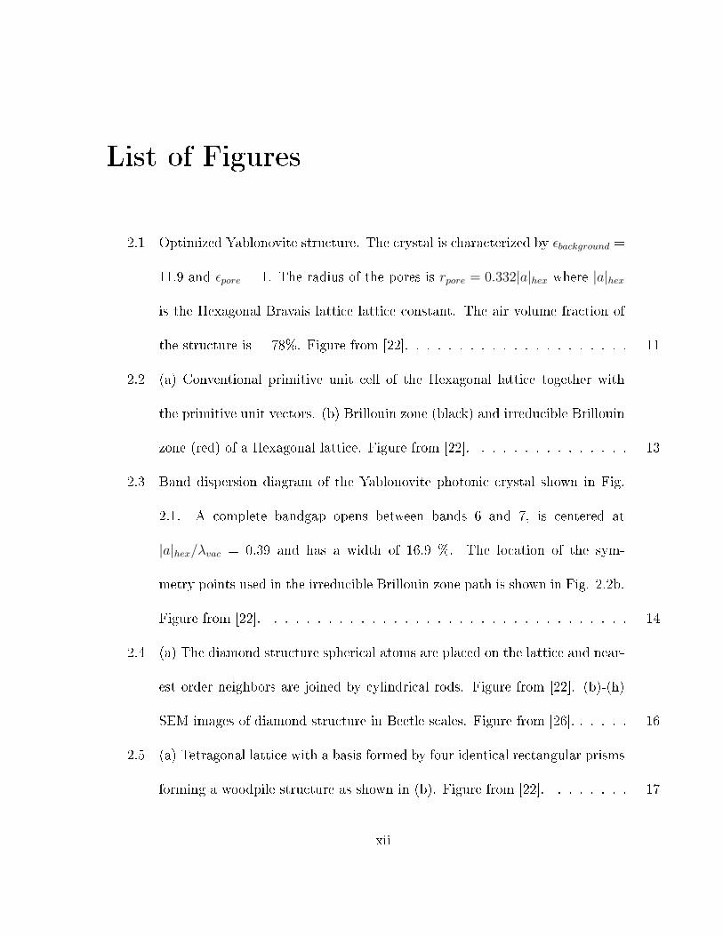
2.1 Optimized Yablonovite structure. The crystal is characterized by εbackground =
11.9 and εpore = 1. The radius of the pores is rpore = 0.332|a|hex where |a|hex
is the Hexagonal Bravais lattice lattice constant. The air volume fraction of
the structure is = 78%. Figure from [22]. . . . . . . . . . . . . . . . . . . . . 11
2.2 (a) Conventional primitive unit cell of the Hexagonal lattice together with
the primitive unit vectors. (b) Brillouin zone (black) and irreducible Brillouin
zone (red) of a Hexagonal lattice. Figure from [22]. . . . . . . . . . . . . . . 13
2.3 Band dispersion diagram of the Yablonovite photonic crystal shown in Fig.
2.1. A complete bandgap opens between bands 6 and 7, is centered at
|a|hex/λvac = 0.39 and has a width of 16.9 %. The location of the sym-
metry points used in the irreducible Brillouin zone path is shown in Fig. 2.2b.
Figure from [22]. . . . . . . . . . . . . . . . . . . . . . . . . . . . . . . . . . 14
2.4 (a) The diamond structure spherical atoms are placed on the lattice and near-
est order neighbors are joined by cylindrical rods. Figure from [22]. (b)-(h)
SEM images of diamond structure in Beetle scales. Figure from [26]. . . . . . 16
2.5 (a) Tetragonal lattice with a basis formed by four identical rectangular prisms
forming a woodpile structure as shown in (b). Figure from [22]. . . . . . . . 17
xii
2.6 Scheme (a) and SEM (b) of woodpile photonic crystals fabricated by the layer-
by-layer approach. Figure from [8]. . . . . . . . . . . . . . . . . . . . . . . . 18
2.7 SEM of (a) silica opal and (b) Si inverted opal. Figure from [28]. . . . . . . 20
2.8 Three-dimensional photonic crystals fabricated by direct laser writing (DLW).
(a) Woodpile structure with 40 layers and a massive wall that prevents bend-
ing and reduces distortions due to polymer shrinkage during polymerization,
completely fabricated by DLW. (b) Cross and (c) top view of a di�erent bro-
ken sample with 12 layers, illustrating the sample quality obtained with the
DLW process. Figure from [9]. . . . . . . . . . . . . . . . . . . . . . . . . . . 21
2.9 (a) Schematic of four beam interference setup for holographic lithography pro-
ducing 3D interference pattern in the beam overlap region. Figure from [22].
SEM images from Ref. [12] of the (b) polymeric photonic crystal fabricated by
exposure of photoresist to a interference pattern shown in Fig. 1A of Ref. [12]
(scale bars 10 µm). Close-up view of top surface (c) and cross-section (d) of
the structure shown in part (a) (scale bars 1 µm). . . . . . . . . . . . . . . . 23
2.10 Body-centred-tetragonal (BCT) symmetry structure fabricated using binary
2D DOE. Inset (a)-(c) shows top view and inset-(b)-(d) shows cross-sectional
SEM views. Figure from [14]. . . . . . . . . . . . . . . . . . . . . . . . . . . 25
2.11 Scanning electron microscope image woodpile-type photonic crystal recorded
in the SU-8 photoresist (a) top view of the photonic structure and (b) cross-
section view of the photonic structure. Figure from [15]. . . . . . . . . . . . 25
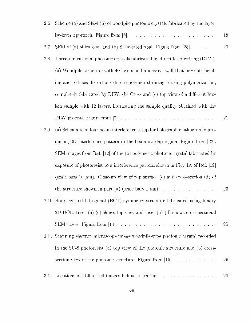
3.1 Locations of Talbot self-images behind a grating. . . . . . . . . . . . . . . . 29
xiii
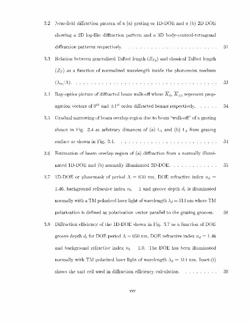
3.2 Near-�eld di�raction pattern of a (a) grating or 1D-DOE and a (b) 2D DOE
showing a 2D log-like di�raction pattern and a 3D body-centred-tetragonal
di�raction patterns respectively. . . . . . . . . . . . . . . . . . . . . . . . . 31
3.3 Relation between generalized Talbot length (ZTg) and classical Talbot length
(ZT ) as a function of normalized wavelength inside the photoresist medium
(λm/Λ). . . . . . . . . . . . . . . . . . . . . . . . . . . . . . . . . . . . . . . 33
3.4 Ray-optics picture of di�racted beam walk-o� where K0, K±1 represent prop-
agation vectors of 0th and ±1st order di�racted beams respectively. . . . . . 34
3.5 Gradual narrowing of beam overlap region due to beam �walk-o�� of a grating
shown in Fig. 3.4 at arbitrary distances of (a) L1 and (b) L2 from grating
surface as shown in Fig. 3.4. . . . . . . . . . . . . . . . . . . . . . . . . . . 34
3.6 Estimation of beam overlap region of (a) di�raction from a normally illumi-
nated 1D-DOE and (b) normally illuminated 2D-DOE. . . . . . . . . . . . . 35
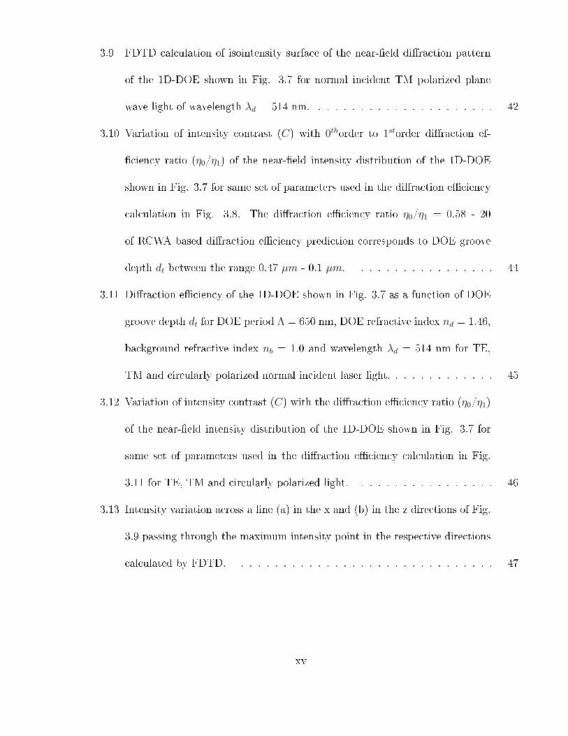
3.7 1D-DOE or phasemask of period Λ = 650 nm, DOE refractive index nd =
1.46, background refractive index nb = 1 and groove depth dt is illuminated
normally with a TM polarized laser light of wavelength λd = 514 nm where TM
polarization is de�ned as polarization vector parallel to the grating grooves. 38
3.8 Di�raction e�ciency of the 1D-DOE shown in Fig. 3.7 as a function of DOE
groove depth dt for DOE period Λ = 650 nm, DOE refractive index nd = 1.46
and background refractive index nb = 1.0. The DOE has been illuminated
normally with TM polarized laser light of wavelength λd = 514 nm. Inset-(i)
shows the unit cell used in di�raction e�ciency calculation. . . . . . . . . . 39
xiv
3.9 FDTD calculation of isointensity surface of the near-�eld di�raction pattern
of the 1D-DOE shown in Fig. 3.7 for normal incident TM polarized plane
wave light of wavelength λd = 514 nm. . . . . . . . . . . . . . . . . . . . . . 42
3.10 Variation of intensity contrast (C) with 0thorder to 1storder di�raction ef-
�ciency ratio (η0/η1) of the near-�eld intensity distribution of the 1D-DOE
shown in Fig. 3.7 for same set of parameters used in the di�raction e�ciency
calculation in Fig. 3.8. The di�raction e�ciency ratio η0/η1 = 0.58 - 20
of RCWA based di�raction e�ciency prediction corresponds to DOE groove
depth dt between the range 0.47 µm - 0.1 µm. . . . . . . . . . . . . . . . . 44
3.11 Di�raction e�ciency of the 1D-DOE shown in Fig. 3.7 as a function of DOE
groove depth dt for DOE period Λ = 650 nm, DOE refractive index nd = 1.46,
background refractive index nb = 1.0 and wavelength λd = 514 nm for TE,
TM and circularly polarized normal incident laser light. . . . . . . . . . . . . 45
3.12 Variation of intensity contrast (C) with the di�raction e�ciency ratio (η0/η1)
of the near-�eld intensity distribution of the 1D-DOE shown in Fig. 3.7 for
same set of parameters used in the di�raction e�ciency calculation in Fig.
3.11 for TE, TM and circularly polarized light. . . . . . . . . . . . . . . . . 46
3.13 Intensity variation across a line (a) in the x and (b) in the z directions of Fig.
3.9 passing through the maximum intensity point in the respective directions
calculated by FDTD. . . . . . . . . . . . . . . . . . . . . . . . . . . . . . . 47
xv

3.14 Relative motif shape of the intensity distribution shown in Fig. 3.9 corre-
sponding to motif shape factor Sf = 1.63, 4.7 and 3 for TE, TM and circularly
polarized light, respectively, for a constant di�raction e�ciency ratio η0/η1 =
1 for all three polarization. . . . . . . . . . . . . . . . . . . . . . . . . . . . 48
3.15 Change of �lling fraction as a function of exposure dose of the intensity dis-
tribution shown in Fig. 3.9. . . . . . . . . . . . . . . . . . . . . . . . . . . . 49
3.16 (a) Closed-packed FCC structure of air spheres (nf = 1) in silicon background
(nb = 3.45). (b) Brillouin zone (black) and irreducible Brillouin zone (red) of
a FCC lattice [22]. . . . . . . . . . . . . . . . . . . . . . . . . . . . . . . . . 57
3.17 (a) Analytically computed band diagram of the FCC structure shown in Fig.
3.16. (b) Band diagram of the same structure computed by the numerical
PWE method where the structure has been represented by sampling frequency
Fs = 200 samples/lattice constant. In both analytical as well as numerical
PWE method 1331 plane waves have been used. . . . . . . . . . . . . . . . . 58
3.18 Variation of (a) percentage complete bandgap (4ω/ωo%) and (b) correspond-
ing bandgap centre frequency (aω0/2πc) with number of plane waves of the
structure shown in Fig. 3.16a computed using both numerical PWE as well
as analytical PWE method. . . . . . . . . . . . . . . . . . . . . . . . . . . . 59
3.19 Band computation time of the FCC structure shown in Fig. 3.16a has been
plotted as a function of number of plane wave and sampling frequency. . . . 60
3.20 Variation of (a) percentage bandgap and (b) corresponding bandgap centre
frequency with sampling frequency of the structure shown in Fig. 3.16a. . . 61
xvi

4.1 Diamond-like woodpile structure where a and c are lateral and axial peri-
odicities respectively and S represents centre to centre distance between two
orthogonally rotated log pile structures. Rx and Rz represent radii of elliptical
shaped logs. . . . . . . . . . . . . . . . . . . . . . . . . . . . . . . . . . . . . 64
4.2 Band dispersion diagram (a) for 3D woodpile structure in photoresist for val-
ues of n =1.6, c/a = 1.2, and f ≈ 25% and (b) modi�ed dispersion diagram
with the same structure after double inversion to a silicon woodpile with n =
3.45, c/a = 1.2, and f ≈ 25%. . . . . . . . . . . . . . . . . . . . . . . . . . 67
4.3 Variation of the complete bandgap with λd/Λ ratio for silicon inverted struc-
tures of silicon logs in air background (f ≈25%). . . . . . . . . . . . . . . . 68
4.4 Variation of c/a ratio in SU-8 photoresist (nr = 1.6) with normalized wave-
length λd/Λ for di�erent refractive index values of the incidence medium (ni). 69
4.5 Di�raction e�ciency of the phasemask as a function of groove depth dt for
period Λ = 1.066 µm, DOE refractive index nd = 1.46 and background re-
fractive index nb = 1.0. The phasemask has been illuminated normally with
laser light of wavelength λd = 488 nm having polarization vector parallel to
the grating grooves (TM polarized). . . . . . . . . . . . . . . . . . . . . . . . 71
4.6 Formation of multiple di�racted beams from a single laser beam by a 1D-DOE
and arrangement for photoresist exposure. . . . . . . . . . . . . . . . . . . . 72
4.7 Periodic near-�eld di�raction patterns created by (a) a single exposure with
a 1D-DOE, (b) a single exposure with a similar 1D-DOE rotated by 90o, and
(c) the resulting interlaced 3D woodpile structure due to combination of the
two exposures in (a) and (b) with shift S = c/4 between two exposures. . . 73
xvii
4.8 Phasemask arrangement de�ning a two-dimensional DOE and providing ad-
justable separation, d, for phase shift control of near-�eld di�raction patterns. 75
4.9 The 3D structure representations of DOE near-�eld di�raction patterns gen-
erated by interlacing of two 2D log structures: (a) BCT symmetry structure
for S = 0, and (b) diamond-like woodpile structure with TTR symmetry for
S = c/4. . . . . . . . . . . . . . . . . . . . . . . . . . . . . . . . . . . . . . . 77
4.10 Time averaged intensity pro�les calculated by FDTD for a constant z = zo
plane, for increasing phasemask air gap (ngap= 1) of (a) d = 0.9084 µm, S =
c/4, (b) d = 1.816 µm, S = c/2 (or 0), (c) d = 2.725 µm, S = 3c/4 (or c/4),
and (d) d = 3.634 µm, S = c (or 0). Here, a = Λ= 1.066 µm. . . . . . . . . 79
4.11 (a) A two-level 2D DOE having groove depth of d and equal periodicities of
Λx = Λy=Λ. (b) One typical laser laser exposure arrangement showing index
matching medium (ni) between DOE substrate (ns) and photoresist (nr) layer
which is spun onto a substrate of refractive index ns. . . . . . . . . . . . . . 81
4.12 A three-level DOE (a) color-coded for each phase level as de�ned by orthogonal
grooves of periodicities Λx and Λy, depths d1 and d2 and refractive indices nd1
and nd2 in a background medium of refractive index nb; and (b) laser exposure
arrangement showing index matching medium (ni) between DOE substrate
(ns) and photoresist (nr) layer which is spun onto a substrate of refractive
index ns. . . . . . . . . . . . . . . . . . . . . . . . . . . . . . . . . . . . . . 81
xviii

4.13 Di�raction e�ciency of a three-level DOE (Fig. 4.12a) as a function of groove
depth d1 with a �xed groove di�erence (d2 - d1) = 331 nm for diamond-
like structure. Inset (i) shows the unit cell with d2 and d1 phase elements
of refractive index, nd = 1.6, in air background (nb = 1.0) and substrate
refractive index ns =1.46. . . . . . . . . . . . . . . . . . . . . . . . . . . . . 84
4.14 Near-�eld isointensity distribution computed by FDTD showing a single basis
BCT symmetry structure as expected from the two-level DOE of Λ = 570 nm,
d = 0.565 µm, nd = 1.46. Inset (b) and (c) shows 2D intensity distribution
(<I(x, y)>) of two planes clearly shows the BCT symmetry of the single basis
structure. . . . . . . . . . . . . . . . . . . . . . . . . . . . . . . . . . . . . . 86
4.15 Near-�eld isointensity distribution computed by FDTD showing woodpile
structure with clear o�set S = c/4 between two orthogonally rotated logs
as expected from the three-level DOE design of Λ = 650 nm, d1 = 1.13 µm,
d2 = 1.46 µm, nd = 1.6 and nb = 1.0. Inset (b) and (c) shows 2D intensity
distribution (<I(x, y)>) of two planes separated axially by S = c/4 = 615
nm distance which show orthogonally rotated log like intensity distributions
as expected for a woodpile structure. . . . . . . . . . . . . . . . . . . . . . . 87
5.1 Beam delivery system. Mn= turning mirrors, An= alignment apertures, HWP
= half waveplate, QWP = quarter waveplate, SF = spatial �lter assembly
consists of objective lens of NA = 0.1 and gold plated pinhole of diameter =
10 µm, L1= collimating lens, BE = beam expander, Ab= exposure beam size
selecting aperture, ES = electronic shutter, VP = vacuum pump. . . . . . . 90
xix

5.2 The photograph of the actual experimental beam delivery system. Important
components have been labeled. . . . . . . . . . . . . . . . . . . . . . . . . . . 91
5.3 Argon ion beam pro�le (a)-(b) before mirror M1, (c)-(d) after aperture A7
and (e)-(f) after aperture Abas depicted in Fig. 5.1. . . . . . . . . . . . . . 92
5.4 Absorption of H-Nu photoinitiators. . . . . . . . . . . . . . . . . . . . . . . . 93
6.1 Double laser exposure based diamond-like woodpile photonic crystal fabrica-
tion technique. . . . . . . . . . . . . . . . . . . . . . . . . . . . . . . . . . . 99
6.2 Top SEM view (a) of the DOE fabricated 3D photonic crystal template to-
gether with cross-sectional view (b), showing 9 layers in the SU-8 photoresist.
Inset (ii) shows magni�ed version of cross-section and inset (i) and inset (iii)
shows interference equation based iso-intensity surface predictions. . . . . . 100
6.3 Laser exposure setup of back to back connected two 1D-DOE forming a phase
tunable DOE. . . . . . . . . . . . . . . . . . . . . . . . . . . . . . . . . . . . 103
6.4 Top (a) and cross-sectional (b) SEM images of diamond-like woodpile struc-
ture with TTR symmetry fabricated using phase-tunable DOE method to-
gether with insets (i) and (ii), respectively, of matching isointensity surfaces
computed by FDTD for d = 2.725 µm and corresponding to S = c/4. . . . . 104
6.5 Top (a) and cross-sectional (b) SEM images of structure with BCT symmetry
fabricated using phase-tunable DOE method together with insets (i) and (ii),
respectively, of matching isointensity surfaces computed by FDTD for d =
3.634µm and corresponding to S = c. . . . . . . . . . . . . . . . . . . . . . . 105
xx
6.6 Top (a) and cross-sectional (b) SEM images of diamond-like woodpile struc-
tures having TTR symmetry together with insets (i) and (ii), respectively, of
corresponding intensity distribution (<I(x,y)>) computed by FDTD for d =
2.725 µm air gap between two phasemasks corresponding to shift S = c/4. . 106
6.7 Band calculation (a) for double exposure formed woodpile template (f = 64%,
c/a = 5.97, nr= 1.6) shown in Fig. 6.2 and (b) infrared spectral recording
along Γ-Z direction. (c) The Brillouin zone of the tetragonal lattice displaying
scan path used in band calculation of (a) [22]. . . . . . . . . . . . . . . . . . 109
6.8 Telecom-band transmission spectra through a woodpile template (Fig. 6.2)
for various angles of incidence (degree) from the sample normal. . . . . . . . 111
7.1 Atomic force microscope image of the two-level DOE of period Λx = Λy =
570 nm and etch depth dt = 595 nm. Inset (i) show single-line height pro�le
that de�ne groove depths dt (Length of scale bars as indicated). . . . . . . . 116
7.2 Atomic force microscope image of the three-level DOE represented by the
three di�erent colors (heights). Enlarged section identi�es a unit cell abcd
(iii) and the ideal height pro�le ABCD (iv) used in the FDTD simulation.
Inset (i) and (ii) show single-line height pro�les in orthogonal scan directions
that de�ne groove depths d2 and d1 (Length of scale bars as indicated). . . . 118
7.3 Laser exposure arrangement of a (a) two-level DOE and (b) the proposed
three-level DOE showing index matching medium (ni) between DOE substrate
(ns) and photoresist (nr) layer which is spun onto a substrate of refractive
index ns. . . . . . . . . . . . . . . . . . . . . . . . . . . . . . . . . . . . . . 119
xxi
7.4 Top (a) and cross-sectional (c) SEM images of the BCT symmetry structure
in SU-8 photoresist. Inset-(iii) and (iv) shows enlarged views of top and cross-
section. Inset-(i) and (ii) shows corresponding predicted near-�led isointensity
surfaces computed by FDTD. . . . . . . . . . . . . . . . . . . . . . . . . . . 120
7.5 Top (a) and manually cleaved cross-sectional (b) SEM images of diamond-
like woodpile structure in SU-8 photoresist showing 40 layers together with
insets (i) and (iii), respectively, of predicted near-�led isointensity surfaces
computed by FDTD. Inset (iv) shows enlarged view of cross-section of the
actual structure and inset (ii) shows corresponding enlarged view of predicted
isointensity surface of inset (iii) [36]. . . . . . . . . . . . . . . . . . . . . . . 121
7.6 Band diagram (a) of the structure shown in Fig. 7.5 revealing a Γ-Z direction
(normal incidence) (c-axis) stopband between the 5th and 6th band and cor-
responding normalized transmission spectrum (b) measured as normal angle
of incidence through the structure in Fig. 7.5b showing a strong (-30 dB)
stopband at 1.306 µm. . . . . . . . . . . . . . . . . . . . . . . . . . . . . . . 124
8.1 Transmission recording of Γ-Z stopband of the woodpile structure shown in
Fig. 7.5 of Chapter 7 during Ethanol immersion (t = 0+ ) and evaporation (t
> 0+) and corresponding comparison with air-�lled photonic crystal spectrum
(t = 0-). . . . . . . . . . . . . . . . . . . . . . . . . . . . . . . . . . . . . . 131
xxii

8.2 (a) Laser exposure setup for single laser exposure fabrication of 3D periodic
structure and micro-�uidic channels using a combination of di�ractive and am-
plitude mask and (b) an amplitude mask for preferential masking of di�racted
light to de�ne open channels. Two layers of index matching medium (ni) have
been used between DOE substrate (ns) and amplitude mask (nAM) and also
between amplitude mask and photoresist (nr) layer which is spun onto a sub-
strate of refractive index ns. . . . . . . . . . . . . . . . . . . . . . . . . . . 132
8.3 (a) Micro-�uidic channel inside 3D structure and (b) enlarged view of the
embedded 3D photonic crystal structures. . . . . . . . . . . . . . . . . . . . 133
8.4 Top (a) and cross-sectional (b) SEM images of SiO2 coated BCT symmetry
structure. (c) and (d) corresponding top and cross-sectional views after SiO2
over-layer removal. (e) FIB milled cross-section after removal of SU-8 template
and the corresponding enlarged cross-sectional view is shown in (f). EDX
spectra (g) and material composition (h) showing ∼90% presence of SiO2 in
the inverted structure. . . . . . . . . . . . . . . . . . . . . . . . . . . . . . . 136
8.5 Normalized transmission spectrum measured as normal angle of incidence
through the structure in Fig. 8.4e showing a strong (-28 dB) stopband at
1.296 µm. . . . . . . . . . . . . . . . . . . . . . . . . . . . . . . . . . . . . . 137
9.1 The photograph of a large area uniform 3D sample with four di�erent viewing
angles (a)-(d). (e) top SEM view of the sample. . . . . . . . . . . . . . . . . 142
A.1 Interference of di�racted beams from a phasemask inside a medium of refrac-
tive index (nr). . . . . . . . . . . . . . . . . . . . . . . . . . . . . . . . . . . 148
xxiii

Published Work
Journal publications as �rst author
[1] D. Chanda, L. E. Abolghasemi, M. Haque, M. L. Ng, P. R. Herman, �Multi-level
Di�ractive Optics for Single Laser Exposure Fabrication of Telecom-Band Diamond-like 3-
Dimensional Photonic Crystals�, Optics Express, Vol. 16, Issue 20, pp. 15402-15414, Sept
2008.
[2] D. Chanda, L. Abolghasemi, P. R. Herman, �Single Laser Exposure Fabrication of
Diamond-Like 3-Dimensional Photonic Crystal Microstructures using Circularly Polarized
Light�, Applied Physics A 93, 33-37 (2008).
[3] D. Chanda, P. R. Herman, �Phase tunable multilevel di�ractive optical element based
single laser exposure fabrication of three-dimensional photonic crystal templates�, Applied
Physics Letters 91, 061122, Aug 2007.
[4] D. Chanda, L. Abolghasemi, P. R. Herman, �One-dimensional di�ractive optical ele-
ment based fabrication and spectral characterization of three-dimensional photonic crystal
templates�, Optics Express, Vol. 14, Issue 19, pp. 8568-8577, Sept 2006.
[5] D. Chanda, Nicole Zacharia, Moez Haque, P. R. Herman, �Silica inversion of polymer
3-dimensional periodic nanostructures�, Applied Physics Letters, (will be submitted).
[6] D. Chanda, Moez Haque, P. R. Herman, �Complete Numerical Recipe for Band Calcula-
tion of 3-Dimentional Periodic Structures with Regular or Irregular Motifs�, JOSA-B, (will
be submitted).
[7] D. Chanda, P. R. Herman, �E�ect of polarization on near-�eld di�raction pattern�, Optics
Letters, (will be submitted).
xxiv
Conference proceedings as �rst author
[1] D. Chanda, N. Zachari, M. Haque, L. Yuan, M. L. Ng, P. R. Herman, �Inversion of 3-
dimensional polymer photonic crystal fabricated by di�ractive optics laser lithography�, in
Conference on Lasers and Electro-Optics/Quantum Electronics and Laser Science Conference
2009 (CLEO-2008) (submitted).
[2] D. Chanda, L. Abolghasemi, P. R. Herman, �Di�ractive optic near-�eld interference based
fabrication of telecom band diamond-like 3-dimensional photonic crystals,� in Conference on
Lasers and Electro-Optics/Quantum Electronics and Laser Science Conference 2008 Techni-
cal Digest (CLEO-2008), CWO2.
[3] D. Chanda, L. Abolghasemi, P. R. Herman, �Multi-level di�ractive optics for single laser
exposure fabrication of telecom-band three-dimensional photonic crystals�, Proc. of SPIE,
(Photonics West 2008, San Jose), Photonic Crystal Materials and Devices IV.
[4] D. Chanda, P. R. Herman, �Single Laser Exposure Fabrication of 3-Dimensional Photonic
Crystal Microstructures�, Conference on Laser Ablation 2007 Technical Digest.
[5] D. Chanda, L. Abolghasemi, P. R. Herman, �Di�ractive Optical Elements based Single-
Step Fabrication of 3-Dimensional Photonic Crystal Templates,� in Conference on Lasers
and Electro-Optics/Quantum Electronics and Laser Science Conference Technical Digest
(CLEO-2007,Optical Society of America), CThW4, ISBN:1-55752-834-9.
[6] D. Chanda, L. Abolghasemi, P. R. Herman, �Two-dimensional di�ractive optical element
based fabrication of 3D photonic crystal templates�, Proc. of SPIE Vol. 6480, 64800Q,
(2007), Photonic Crystal Materials and Devices IV.
[7] D. Chanda, P. R. Herman, �Di�ractive Optical Elements based Fabrication of Photonic
Crystals�, in Conference on Lasers and Electro-Optics 2006 Technical Digest (CLEO-2006,
xxv

Optical Society of America, 2006), CMV7.
[8] D. Chanda, L. Abolghasemi, P. R. Herman, �Numerical Band Calculation of Holograph-
ically Formed Periodic Structures with Irregular Motif�, Proc. SPIE Vol. 6128, p. 311-316,
2006, Photonic Crystal Materials and Devices IV.
xxvi
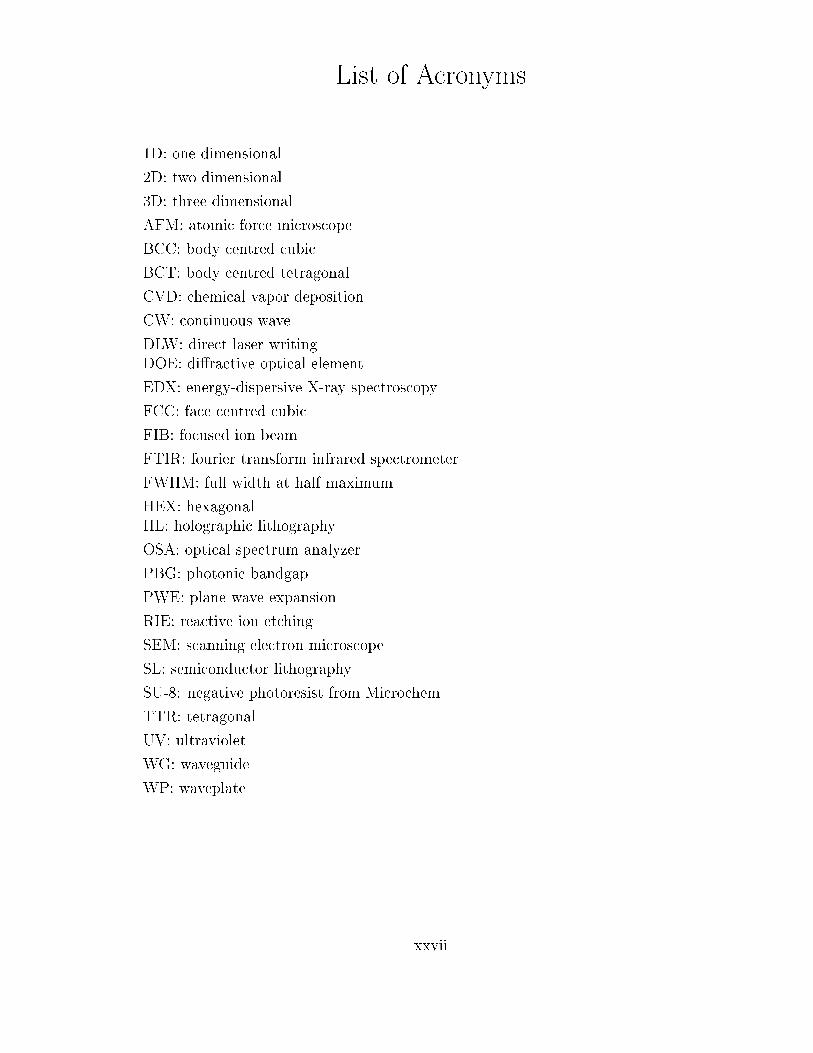
List of Acronyms
1D: one dimensional
2D: two dimensional
3D: three dimensional
AFM: atomic force microscope
BCC: body centred cubic
BCT: body centred tetragonal
CVD: chemical vapor deposition
CW: continuous wave
DLW: direct laser writingDOE: di�ractive optical element
EDX: energy-dispersive X-ray spectroscopy
FCC: face centred cubic
FIB: focused ion beam
FTIR: fourier transform infrared spectrometer
FWHM: full width at half maximum
HEX: hexagonalHL: holographic lithography
OSA: optical spectrum analyzer
PBG: photonic bandgap
PWE: plane wave expansion
RIE: reactive ion etching
SEM: scanning electron microscope
SL: semiconductor lithography
SU-8: negative photoresist from Microchem
TTR: tetragonal
UV: ultraviolet
WG: waveguide
WP: waveplate
xxvii

Chapter 1
Introduction
Light has played a signi�cant role in the advancement of science and technology. The advent
of coherent light from the laser in the 1960s [1,2] has triggered the new era of scienti�c explo-
ration with light. Further desire to manipulate light to explore the fundamental limits has
led to the proposal of the three-dimensional (3D) periodic structures or photonic crystals at
the end of 1980s [3,4]. The three dimensionally periodic materials are arti�cial media which
possess the ability of molding electromagnetic waves without absorption in similar way as
electronic crystals act on electron waves. These 3D periodic structures are becoming a pow-
erful tool for the manipulation of photons to fabricate interesting optical devices like �lters,
lasers, resonators and splitters. Demonstrations of physically interesting phenomena, such as
the suppression or enhancement of light emission, have been pursued from the initial stages
of photonic crystal research. Recently, highly functional integrated photonic chips and the
application of photonic bandgap properties to optical quantum information processing have
also been demonstrated. The conceptual development of 3D photonic crystals had lead to the
study of the two-dimensional (2D) photonic crystals at the end of 1991 [5,6]. A 2D photonic
crystal is characterized by a two dimensional periodicity in the xy plane and by translational
invariance along the z direction. This clearly indicates that light can propagate freely along
1
the z direction and as a consequence the most important property of a 3D photonic crystal,
namely, light con�nement along all 4π directions or a complete bandgap, is not available in
2D case. Hence, for complete control of light, 3D photonic crystals are required. Apart from
optical applications, these porous 3D periodic structures are also attractive as an arti�cially
structured sca�old for biological and chemical applications. However, nano-scale fabrication
of such complex arti�cial periodic structures pose a huge technological challenge. This has
opened up vast opportunities for researchers to explore new 3D nanostructure fabrication
techniques.
1.1 Motivation
For practical applications of three-dimensional nano-scale periodic structures, one needs to
develop simpler and lower cost mass fabrication techniques of high precision. Unlike, two-
dimensional planer structures, large-scale fabrication of 3D periodic structures using stan-
dard semiconductor lithographic technology is extremely tedious and costly due to repeated
fabrication of multiple layers in the z direction [7,8]. Even a �exible fabrication approach like
laser direct writing where a tightly focused laser beam is used for photo-polymerization of 3D
structures inside photo-sensitive materials becomes unacceptably time consuming for indus-
trial batch fabrication even when processing sample sizes of only 100 x 100 microns [9, 10].
Colloidal self-assembly is limited to only face-centred-cubic (FCC) symmetry structure and
is highly susceptible to stacking faults of the self-assembled spheres [11]. Holographic lithog-
raphy (HL) based on interference of multiple laser beams has, in part, met these criteria
by providing a large variety of photonic crystal templates in photo-sensitive materials [12].
However, the inherent vibrational instability of multiple beam splitters and mirrors over large
2

beam paths introduce signi�cant phase and angle errors during the exposure that distort and
blur the 3D structure and also lead to uncontrolled symmetry due to random phase relation
between interfering beams, making reproducibility an extreme challenge. In this context
there is a promising alternative di�ractive optics approach for creating multiple interfering
laser beams in various di�raction orders from a single laser beam incident on a di�ractive
optical element (DOE). The multiple beams are inherently phase-locked to provide stable 3D
near-�eld di�raction patterns without the instability problems of multi-beam HL. The con-
cept behind 3D near-�eld di�raction pattern is well known since mid eighteen hundreds [13].
Rogers and coworkers [14] were �rst to demonstrate the formation of 3D periodic structures
in photoresist using conformal phasemask DOEs. Lin et al. extended DOEs to the fabri-
cation of 3D �Woodpile�-type photonic crystal templates in photoresist by double exposures
of orthogonal phasemasks or one-dimensional DOEs (1D-DOE) [15]. However, imprecise
alignment between two DOE exposures prevents this method from reproducibly generate 3D
structures and a single exposure DOE method is therefore preferred for convenience and im-
proved uniformity of the 3D structure. Further, 3D structures with smaller lattice constants
are required for optical response in telecom band.
The biggest motivation of the present work is to design functional di�ractive optics which
will simplify 3D fabrication to a single laser beam and single optical element based approach
where 3D crystal symmetry, lattice constants and basis information are encoded in the di�rac-
tive element design. Further, design of multi-level di�ractive optical elements will allow one
to manipulate the relative phase of di�racted beams to create complex near-�eld di�raction
patterns. Special attention will be given to create diamond-like near-�eld intensity distribu-
tion due to its wide complete bandgap. Such near-�eld di�raction patterns will be captured
3

inside photosensitive materials to provide 3D photonic crystals of low refractive index con-
trast which will o�er partial stopgaps along few preferential crystallographic directions. One
objective will be to reduce axial to lateral crystal axis ratio (c/a) so that stopbands shift into
the 1.25-1.65 µm telecom band. In principle, a complete photonic bandgap can be achieved
by using a high refractive index photoresist or inverting these low refractive index templates
with high refractive index materials [16].
1.2 New contributions
The main objective of this dissertation is to advance the di�ractive optics based lithogra-
phy technique to fabricate a wide range of three-dimensional periodic nanostructures. The
complete process involved theoretical development, design, computation, modeling and fab-
rication. In this process, new contributions were made in several areas.
Photonic band calculation played an important role in predicting bandgap locations of 3D
periodic structures. Isointensity surfaces were calculated from the design of di�ractive optics
which was followed with bandgap calculations to optimize the bandgap properties of the
expected 3D templates both in photoresist and after inversion in silicon. A numerical band
calculation code was developed as part of the present research work. Novel digital �ltering
techniques were implemented in the numerical band calculation algorithm to improve band
calculation accuracy and reduce computation time enormously by approximately 1000 times
which accelerated the progress of this research work.
For selecting a exposure laser and DOE period, the relation between crystal lattice con-
stants with exposure laser wavelength and DOE period has been established. Detailed de-
sign criteria of all four proposed di�ractive optics methods have been presented which were
4

supported with �nite di�erence time domain (FDTD) prediction of near-�eld intensity dis-
tributions and numerical band calculation of expected band dispersion relations.
A diamond-like woodpile structure was �rst formed with di�ractive optic near-�eld lithog-
raphy by two sequential laser exposures of photoresist using orthogonally rotated 1D binary
phasemasks. To overcome the inherently imprecise DOE alignment that arises between two
laser exposures, a single laser exposure fabrication of 3D photonic crystals was devised by
back-to-back mounting of two linear phasemasks with crossed grating orientation. This de-
�ned a phase-tunable DOE that permitted the �rst single exposure near-�eld lithography
based fabrication of the diamond-like structure.
The phase-tunable DOE further o�ered formation of a continuum of other 3D periodic
structures that were tunable from the double basis diamond-like structure to a single basis
structure having body-centered-tetragonal symmetry (BCT) by simply tuning the phase
di�erence (π /2 to 0 radian) of one set of �rst order di�racted beams.
Although, the phase tunable near-�eld DOE method is versatile, it requires accurate
physical separation of the two orthogonally rotated gratings in order to provide a quarter
period shift between two orthogonal interference patterns required for diamond-like woodpile
structure. To improve fabrication reproducibility of diamond-like structure, a single-surface
multi-level DOE device with an appropriate �xed phase-shift optimized for formation of
diamond-like photonic crystal structure in a single laser exposure step was proposed. Finite
di�erence time domain (FDTD) calculation of near-�eld di�raction patterns were corrobo-
rated by de�nitive demonstrations of diamond-like woodpile structure inside the photoresist
as predicted.
This new multi-level DOE was fabricated and tested experimentally, permitting a large
5
number of layers (> 40) to form in thick photoresist. A record strength -30 dB stopband at
1.306 µm telecom band was observed. The usefulness of this stopband for refractive index
sensing of liquids has been demonstrated. These low refractive index polymer structures were
inverted with amorphous silica to convert a �soft� polymer structure to a robust structure
made with a �hard� material. The high quality silica inverted structure promises possible
use in biological sensing applications and also serves well for possible silicon double inversion
for fabricating silicon 3D photonic crystals with a complete bandgap.
1.3 Overview of the dissertation
The dissertation is comprised of theoretical and experimental works and have been divided
into separate chapters as follows:
In Chapter 2, the origin of three-dimensional periodic structure is reviewed. The theory
behind the photonic bandgap has been discussed brie�y. Di�erent micro and nano fabrication
techniques of 3D periodic structures have been described with merits and de-merits of each
method is discussed.
In Chapter 3, the theoretical foundation of the present research work has been laid out.
The under-lying physics behind di�ractive optics lithography has been discussed in terms
of Talbot self-imaging phenomenon. The beam walk-o� has been characterized to de�ne a
practical working depth of near-�eld lithography. E�ects of relative di�raction e�ciency and
laser polarization on near-�eld intensity distribution have been assessed with �nite di�erence
time domain (FDTD) calculations. The theory behind photonic band calculation has been
discussed. Details of numerical band calculation have been elaborated with example band
calculations.
6

In Chapter 4, the objective to create a diamond-like woodpile structure has been de-
scribed. The band diagram of an optimized woodpile structure is presented and corre-
sponding variation of the width of the complete bandgap with laser wavelength (λd) to the
DOE period (Λ) ratio (λd/Λ) has been demonstrated. The theory and design guidelines
of three proposed di�ractive optic approaches for fabricating woodpile structure have been
presented. The design started with 1D di�ractive optics and then moved towards binary and
then multi-level 2D di�ractive optics to improve fabrication precision of 3D structures. Finite
di�erence time domain calculation of near-�eld di�raction patterns and associated isointen-
sity surfaces have been presented to corroborate de�nitive demonstration of a diamond-like
woodpile structure formed inside photoresist.
In Chapter 5, the experimental fabrication and characterization techniques of 3D nanos-
tructure are presented. The argon ion laser and beam delivery system for exposing photore-
sist has been described. The photoresist sample preparation, laser exposure procedures and
structural and optical characterizations of 3D structures are presented.
In Chapter 6, results are presented for one-dimensional di�ractive optics based double
and single laser exposure fabrication of 3D structures. A novel phase control method has
been demonstrated in generating a range of 3D structures, with symmetries from tetragonal
(TTR) through to body-centred-tetragonal (BCT), that o�er �exible tailoring of bandgap
strength, width and spectral dispersion. A relatively long period DOE (Λ = 1.066 µm) pro-
vided 3D templates in SU-8 photoresist that con�rm formation of thick, large area periodic
nanostructures with optical response in the near-infrared band.
In Chapter 7, a novel single laser exposure method of fabricating diamond-like photonic
crystals by multi-level di�ractive optics has been presented. A short-period three-level DOE
7

(Λ = 650 nm) was laser-fabricated and applied to form 3D periodic structures in photoresist
that con�rm formation of thick, large area diamond-like nanostructures closely matching
isointensity predictions of �nite di�erence time domain computation. Spectroscopic charac-
terization of the polymer structure revealed a strong stopband along the Γ-Z direction in the
telecom band that was consistent with calculated band dispersion curves for the low-index
medium.
In Chapter 8, application of strong and narrow stopgaps of polymer 3D photonic crystals
in optical sensing has been demonstrated. A shadow masking technique has been demon-
strated to integrate these 3D structures with micro-�uidic channels. As a �nal step, the
polymer structures have been e�ectively inverted with silica using a chemical vapor deposi-
tion technique. The high quality silica inverted structure promises possible use of inverted
structures in biological sensing applications as well as possible silicon double inversion for
fabricating silicon 3D photonic crystals.
Finally, Chapter 9 concludes the thesis by summarizing the key �ndings and comparing
the di�erent 3D fabrication techniques. An outlook on future research directions have been
outlined.
8
Chapter 2
Background on three-dimensional
periodic structures
Three-dimensional periodic structures are unique in many ways. They form a porous medium
which is attractive as an arti�cial structured environment for fundamental and applied
physics studies. From a wave propagation point of view, the band dispersion relation of
such media possess gaps in the k-space, unlike bulk materials, creating new opportunities in
electromagnetic wave manipulations.
2.1 Brief history of photonic bandgap concept
The phenomenon of coherent back scattering was well known for a long time. Lord Rayleigh
conjectured in 1887 that any arbitrary periodic arrangement of transparent materials will
induce coherent back scattering for a band of frequencies for a speci�c angle of incidence
[17]. This coherent back scattering or partial stopgap of one-dimensional (1D) periodic
structures is known as Bragg re�ection. However, the concept behind a complete photonic
bandgap was proposed independently and simultaneously in 1987 by two researchers, each
following a di�erent path. Sajeev John was formulating a solution to the fundamental
science question of whether photons can be trapped inside a strongly scattering medium like
9
electrons localization inside a disordered media and subsequently proposed that photons can
be localized inside an appropriate arrangement of strong scatterers [4]. At the same time Eli
Yablonovitch was trying to address some of the limitations of semiconductor lasers in terms
of suppression of spontaneous emission [3]. He proposed that the spontaneous emission is
not a fundamental property of matter but rather a characteristic of the coupling between
electromagnetic waves and matter and can be controlled by placing the matter inside an
arti�cially arranged environment. In con�uence of these two lines of thoughts the complete
photonic bandgap concept was born.
Following many unsuccessful trials, Yablonovitch �nally proposed in 1989 a face-centred-
cubic dielectric structure having a complete photonic bandgap [18]. Unfortunately, later
theoretical studies [19] by full vectorial treatment of the Maxwell equations showed that
the structure reported in [18] can not open a complete photonic bandgap. In between,
Ho, Chan and Soukoulis showed that a diamond photonic crystal structure does have a
complete photonic bandgap [20]. This was a very encouraging result which also proved
that symmetry or lack of symmetry of the photonic crystal plays an important role in the
formation of the photonic band structure. At the end of 1991, Yablonovitch, Gmitter and
Leung created the �rst photonic crystal exhibiting a full photonic bandgap at microwave
frequencies [21]. The proposed structure is famously known as Yablonovite, named after
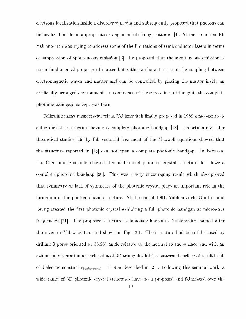
the inventor Yablonovitch, and shown in Fig. 2.1. The structure had been fabricated by
drilling 3 pores oriented at 35.26o angle relative to the normal to the surface and with an
azimuthal orientation at each point of 2D triangular lattice patterned surface of a solid slab
of dielectric constant εbackground = 11.9 as described in [21]. Following this seminal work, a
wide range of 3D photonic crystal structures have been proposed and fabricated over the
10
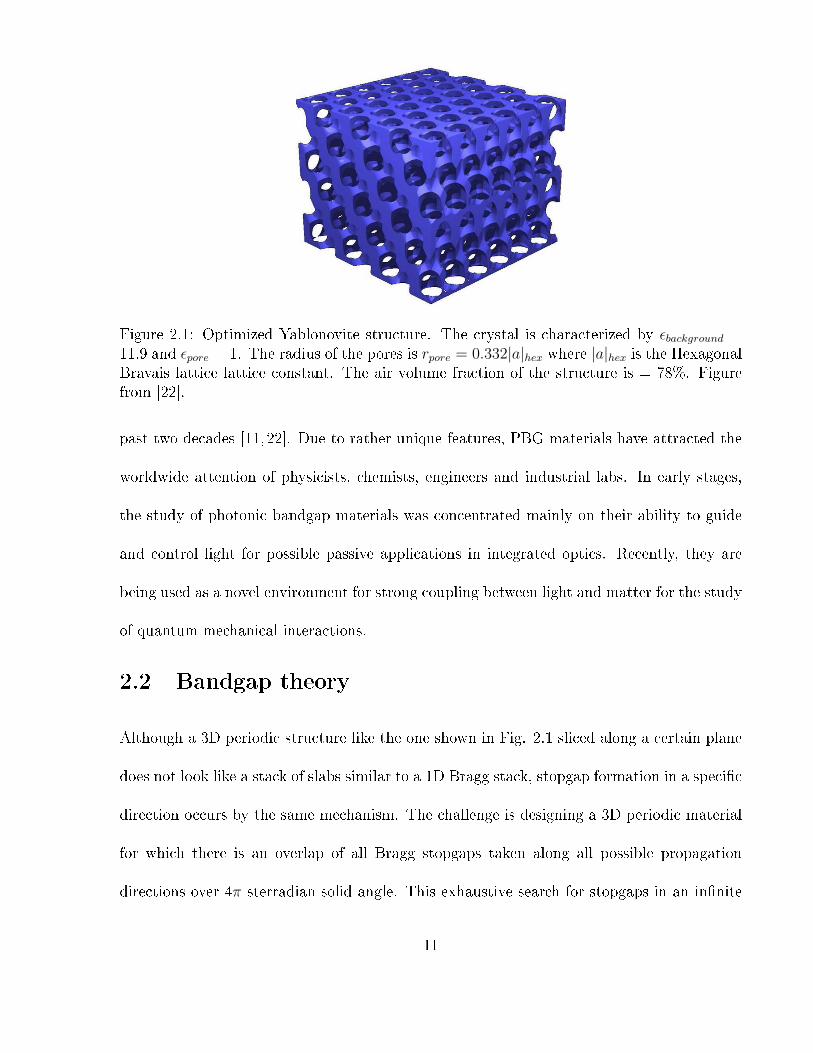
Figure 2.1: Optimized Yablonovite structure. The crystal is characterized by εbackground =11.9 and εpore = 1. The radius of the pores is rpore = 0.332|a|hex where |a|hex is the HexagonalBravais lattice lattice constant. The air volume fraction of the structure is = 78%. Figurefrom [22].
past two decades [11, 22]. Due to rather unique features, PBG materials have attracted the
worldwide attention of physicists, chemists, engineers and industrial labs. In early stages,
the study of photonic bandgap materials was concentrated mainly on their ability to guide
and control light for possible passive applications in integrated optics. Recently, they are
being used as a novel environment for strong coupling between light and matter for the study
of quantum mechanical interactions.
2.2 Bandgap theory
Although a 3D periodic structure like the one shown in Fig. 2.1 sliced along a certain plane
does not look like a stack of slabs similar to a 1D Bragg stack, stopgap formation in a speci�c
direction occurs by the same mechanism. The challenge is designing a 3D periodic material
for which there is an overlap of all Bragg stopgaps taken along all possible propagation
directions over 4π sterradian solid angle. This exhaustive search for stopgaps in an in�nite
11

k-space can be reduced by taking advantage of the symmetry of the periodic structure. It
has been shown that it is su�cient to scan only the irreducible Brillouin zone of the periodic
structure for that purpose. The key factors in the formation of the complete photonic
bandgap are the ones which in�uence the frequency positions and the width of stopgaps.
The shape of the Brillouin zone is important and it is easy to understand that a spherical
shape is desirable for maximum likelihood of overlap of all stopgaps in di�erent directions.
As width of stopgap is directly proportional to refractive index contrast, a large refractive
index contrast of at least ≥ 2 is required inside the unit cell of the periodic structure for
opening up complete bandgap [20].
The spatial periodicity, which characterizes all photonic crystals, is described by means
of Bravais lattices in a formalism completely analogous to the one used in the description
of electronic crystals [23]. A photonic crystal structure is completely characterized by the
distribution of the dielectric forming basis on a point lattice. For a Bravais lattice with
primitive vectors of a1, a2 and a3 , the following equality holds true for all integers n1, n2
and n3: ε(r) = ε(r + n1a1 + n2a2 + n3a3).
Generally the spatial distribution of the dielectric or basis inside the primitive unit cell
can be as complex as we can imagine. Further, the choice of the lattice-basis pair is not
unique. Nevertheless almost all the photonic crystals known today can be described easily
in terms of simpler building blocks. As an example, the Yablonovite photonic crystal shown
in Fig. 2.1 can be modeled as a Hexagonal (HEX) Bravais lattice. The Hexagonal primitive
unit cell and corresponding Brillouin zone has been shown in Fig. 2.2. The primitive unit
call is characterized by primitive vectors a1, a2, a3 and the corresponding reciprocal unit cell
or Brillouin zone is characterized by reciprocal vectors b1, b2 and b3. The six vertices of the
12
Figure 2.2: (a) Conventional primitive unit cell of the Hexagonal lattice together with theprimitive unit vectors. (b) Brillouin zone (black) and irreducible Brillouin zone (red) of aHexagonal lattice. Figure from [22].
Hexagonal irreducible Brillouin zone has been labeled with Roman letters as shown in Fig.
2.2b.
The most important feature of a photonic crystal is its unique electromagnetic charac-
teristics which is completely di�erent from its bulk material optical properties. In order to
�nd this unique �ngerprint, one needs to solve the Maxwell's equations inside the photonic
crystal. The solution of the Maxwell's equations is most e�ectively represented by an band
dispersion diagram. As an example, the band diagram of the Yablonovite photonic crystal
shown in Fig. 2.1 has been calculated by solving Maxwell's equation using the plane wave
expansion method [22] and the result is shown in Fig. 2.3. For the band calculation, the
propagation vector, Kb (Bloch vector), has been chosen along the high symmetry points on
the irreducible Brillouin zone of the Hexagonal Bravais lattice (Fig. 2.2b) following a path
Γ → A → H → K → Γ → A → L → M → Γ → M → K → Γ → L → H → Γ. For each
scan segment, 21 discrete values of Kb have been chosen and for each point the lowest 20
13

Figure 2.3: Band dispersion diagram of the Yablonovite photonic crystal shown in Fig. 2.1.A complete bandgap opens between bands 6 and 7, is centered at |a|hex/λvac = 0.39 and hasa width of 16.9 %. The location of the symmetry points used in the irreducible Brillouinzone path is shown in Fig. 2.2b. Figure from [22].
frequencies (a /λ) have been calculated. This then led to a plot like the one shown in Fig.
2.3 [22].
This mode of representation of the dispersion relation in terms of the band diagram
clearly indicates a full photonic bandgap when it exists. The location and size of various
stopgaps can also be immediately inferred from such a plot. An interesting point is that the
band diagram predictions are completely scalable with the lattice constants of the periodic
structure such that the stopbands appear �xed in the dispersion curves due to the a/λ scaling
of photon energy.
2.3 Three-dimensional periodic structures of special in-
terest
A crystal is de�ned by two parts - lattice and basis. The lattice is the periodic outer frame-
work and the basis is the spatial distribution of the �atom� at each lattice site inside the
14

primitive unit cell. According to crystallography, any three-dimensionally periodic structure
can be classi�ed as one of 14 Bravais lattices [23]. However, for a given lattice, an in�nite
choice of basis sets makes an in�nite number of possible lattice-basis combinations. A wide
range of 3D photonic crystal structures have been proposed and fabricated over the past
two decades and each has been given an name to identify an unique lattice-basis combina-
tion [11, 22]. Among them, diamond and diamond-like structures, which are characterized
by double basis on a face-centered-cubic (FCC) or tetragonal (TTR) point Bravais lattice,
are very attractive for their wide complete bandgap when fabricated with high refractive
index materials [20, 22, 24]. However, fabrication of diamond or diamond-like structures is
challenging and tedious due to the double basis nature of their crystal geometry. The laser
fabrication of these double basis structures is one of the core motivations of the present
research work.
2.3.1 Diamond structure
The diamond structure can be viewed as a FCC lattice with a basis formed by two �atoms"
separated by a segment parallel with the main diagonal of the conventional FCC unit cell
as shown in Fig. 2.4a where spherical atoms are placed on the lattice and nearest order
neighbors are joined by cylindrical rods. It is well known that vibrant colors of butter�ies
and many other creatures found in nature are often due to the presence of some kind of
periodic structure on their body [25]. Recently, it has been discovered that the unique color
of a Beetle is due the presence of diamond structure on their scale [26] as shown in Fig. 2.4b.
From the photonic bandgap point of view, the reduced symmetry of this two atoms
basis of diamond structure is the key factor in the breaking of the unwanted crossing be-
15

Figure 2.4: (a) The diamond structure spherical atoms are placed on the lattice and nearestorder neighbors are joined by cylindrical rods. Figure from [22]. (b)-(h) SEM images ofdiamond structure in Beetle scales. Figure from [26].
tween degenerate bands present in the FCC based photonic crystals previously studied by
Yablonovitch [18]. A large complete photonic bandgap of almost 30% was reported to open
in a diamond photonic crystal made from overlapping air spheres in a background material
with an index of refraction of 3.6 [20]. A sizable (∼16%) bandgap opens in the case of solid
spheres as well.
2.3.2 Diamond-like structure
Another structure which has received considerable attention in the photonic crystal com-
munity is the woodpile structure, which was proposed by Ho, Chan and Soukoulis [24]. A
tetragonal lattice with a basis formed by four identical rectangular prisms forms a woodpile
structure as shown in Fig. 2.5. Due to resemblance with the two sphere diamond basis, the
woodpile structure is called �diamond-like�. The woodpile structure can exhibit a complete
photonic bandgap of 18% between the second and the third band for a 30% silicon volume
�lling fraction.
16

Figure 2.5: (a) Tetragonal lattice with a basis formed by four identical rectangular prismsforming a woodpile structure as shown in (b). Figure from [22].
Due to log-pile like stacking of rods, the woodpile structure is ideally suited for sequential
layer-by-layer fabrication processes. This has been demonstrated both by semiconductor
lithography as well as by laser direct writing [8, 9]. However, these sequential fabrication
techniques are very slow and parallel fabrication of multiple layers is essential for any large
scale fabrication of woodpile photonic crystals.
2.4 Nano fabrication of 3D periodic structures
While the manufacturing of most of 3D photonic crystal structures on millimeter scales is
a more or less a straightforward operation, the nanometer scale fabrication for operation in
the optical domain has proved to be a very challenging task. Here we brie�y discuss several
prominent 3D nanostructure fabrication techniques.
2.4.1 Semiconductor lithography
Micro and nano fabrication of two-dimensional photonic planer structures using electron-
beam or UV lithography is a well known procedure inherited from the well established
17

Figure 2.6: Scheme (a) and SEM (b) of woodpile photonic crystals fabricated by the layer-by-layer approach. Figure from [8].
microelectronics industry. In principle, the simplest way to extend UV lithography to three
dimensional structure fabrication is to use a layer-by-layer approach. In a �rst step, the
surface of a wafer is processed by electron-beam or UV lithography to create a 2D periodic
pattern. The pattern is subsequently transferred to the substrate by dry etching. The next
layer is then added either by deposition and subsequent patterning of a dielectric �lm or by
bonding two pieces of independently patterned wafers at temperatures of several hundreds
degrees Celsius (�wafer fusion� method), followed by removal of one of the substrates [7,
8]. This procedure is repeated several times until the desired number of layers is reached.
The woodpile photonic crystal structure is ideally suited for such a sequential layer-by-
layer approach. Susumu Noda has pioneered such fabrication processes and demonstrated
fabrication of high quality woodpile structures [8] as shown in Fig. 2.6. The woodpile
structure shown in Fig. 2.6b was fabricated using the III�V direct bandgap semiconductors
GaAs and InP having photonic bandgaps at telecommunication wavelengths.
In practice, three-dimensional photonic crystals fabricated by this layer-by-layer fabrica-
tion approach are severely limited by the complexity of the fabrication process to only a few
18

lattice constants in the vertical direction. Additionally, a high degree of accuracy is required
to avoid o�sets between di�erent layers. It is immediately apparent that such a sequential
process is highly time consuming, expensive, and technically very tedious.
2.4.2 Self-assembly
Colloidal self-assembly of silica or polystyrene spheres can be used to fabricate arti�cial
opal photonic crystals via sedimentation techniques where suspended spheres sediment on
the substrate kept inside the colloid forming two equivalent dense packings of spheres with
face-centred-cubic (fcc) or hexagonal-closed-packing (hcp) arrangements. In principle, this
technique allows for simple and inexpensive large-area opal template fabrication [27, 28].
However, a complete photonic bandgap is not achievable for both fcc and hcp opals even
with the refractive index limit of n →∝ [11]. However, to generate a complete bandgap,
opals must be inverted with a high refractive index material. It has been shown in Ref. [29]
that such a silicon inverted opal possesses a complete bandgap of 4.5%. The inversion
can be performed by in�ltrating air voids of opal with high refractive index materials and
subsequent removal of the original spheres by wet chemical etching or plasma etching for
silica and polystyrene, respectively. Figure 2.7 shows SEM images of (a) silica opal and (b)
Si inverted opal from Ref. [28]. The Si inverted opal has been shown to possess complete
bandgap in the telecom band [28].
The success of generating a complete bandgap critically depends on the quality of the
inverted opal templates. Commercially available o�-the-shelf spheres have standard devia-
tions in their diameter on the order of 5% or more. Further, self assembled spheres are prone
towards stacking faults [11]. This introduces su�cient disorder to close the anticipated
19
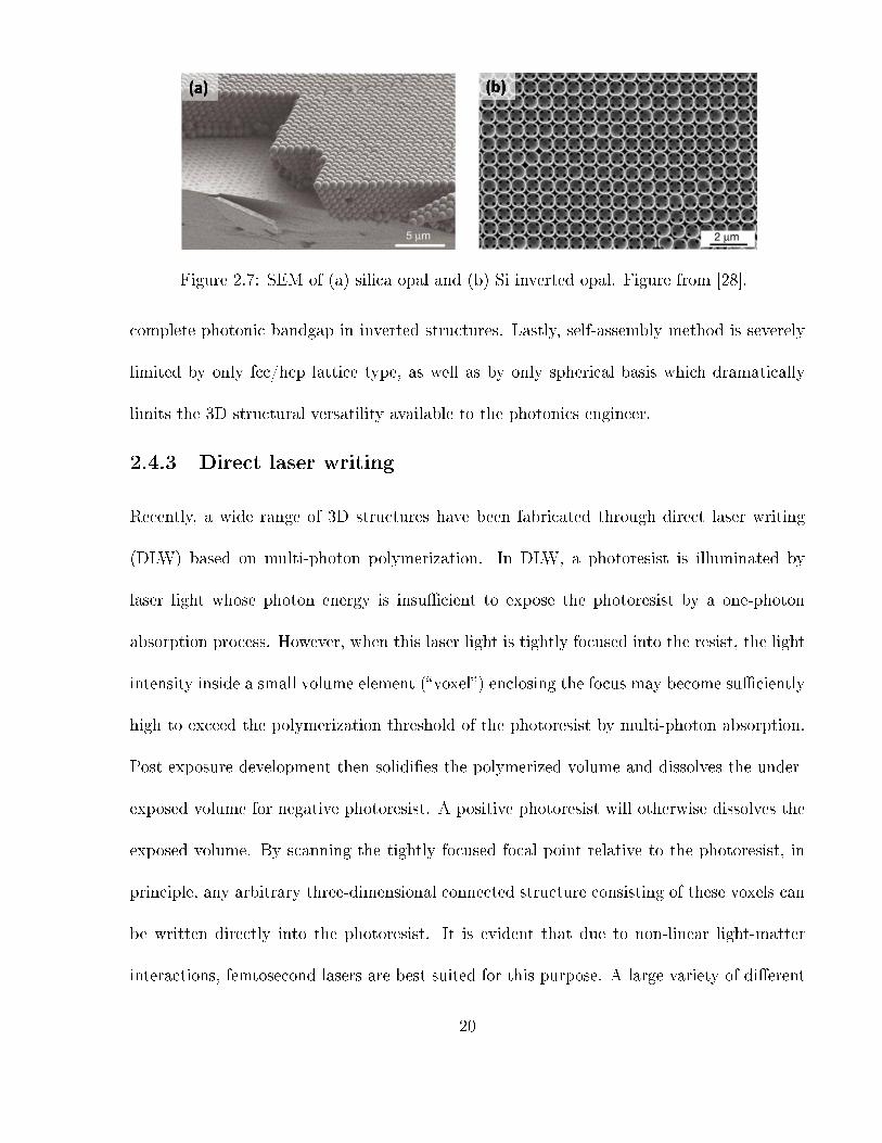
Figure 2.7: SEM of (a) silica opal and (b) Si inverted opal. Figure from [28].
complete photonic bandgap in inverted structures. Lastly, self-assembly method is severely
limited by only fcc/hcp lattice type, as well as by only spherical basis which dramatically
limits the 3D structural versatility available to the photonics engineer.
2.4.3 Direct laser writing
Recently, a wide range of 3D structures have been fabricated through direct laser writing
(DLW) based on multi-photon polymerization. In DLW, a photoresist is illuminated by
laser light whose photon energy is insu�cient to expose the photoresist by a one-photon
absorption process. However, when this laser light is tightly focused into the resist, the light
intensity inside a small volume element (�voxel�) enclosing the focus may become su�ciently
high to exceed the polymerization threshold of the photoresist by multi-photon absorption.
Post exposure development then solidi�es the polymerized volume and dissolves the under-
exposed volume for negative photoresist. A positive photoresist will otherwise dissolves the
exposed volume. By scanning the tightly focused focal point relative to the photoresist, in
principle, any arbitrary three-dimensional connected structure consisting of these voxels can
be written directly into the photoresist. It is evident that due to non-linear light-matter
interactions, femtosecond lasers are best suited for this purpose. A large variety of di�erent
20

Figure 2.8: Three-dimensional photonic crystals fabricated by direct laser writing (DLW).(a) Woodpile structure with 40 layers and a massive wall that prevents bending and reducesdistortions due to polymer shrinkage during polymerization, completely fabricated by DLW.(b) Cross and (c) top view of a di�erent broken sample with 12 layers, illustrating the samplequality obtained with the DLW process. Figure from [9].
structures has been fabricated using femtosecond laser DLW in di�erent kinds of photoresist.
Some high quality 3D structures with su�ciently small lattice constants for stopgaps at
telecommunication wavelengths have been reported by Martin Wegener and Hiroaki Misawa
groups [9, 10]. One such woodpile structure taken from Ref. [9] has been shown in Fig.
2.8. The DLW method was used in fabricating the complete woodpile structure with 40
layers and the massive wall that prevented structural distortions during polymerization.
The main attraction of DLW is that it conceptually allows for the incorporation of any
arbitrary complex shape defect inside a 3D periodic structure.
It has been demonstrated that direct laser writing is capable of delivering high-quality
three-dimensional nanostructures in a versatile fashion. However, to achieve three-dimensional
21

photonic crystals with a complete bandgap, the refractive index of typical photoresists, such
as SU-8 (n = 1.6), is too small. Thus, inversion of these polymer structures with a high re-
fractive index materials is necessary following single or double inversion processes [16,30,31].
The biggest draw back of laser direct writing is the unacceptable processing time when pro-
cessing even for small sample sizes of only 100 µm x 100 µm, precluding DLW as an industrial
batch fabrication technique of 3D micro-nano structures.
2.4.4 Holographic lithography
The main idea behind holographic lithography is to expose a thick photoresist to a standing
light wave pattern originating from the interference of multiple laser beams. A schematic of
four beam interference setup for holographic lithography producing a 3D interference pattern
in the beam overlap region is shown in Fig. 2.9a [22]. It has been theoretically demonstrated
that any of the 14 Bravais lattices in three dimensions should be realizable via holographic
lithography by choosing a proper set of propagation vectors [22]. The �rst 3D structure
fabricated using this technique was reported in March 2000 by Campbell et al. [12]. Figure-
2.9b shows the SEM of corresponding fabricated 3D structure [12]. Subsequently many other
groups independently demonstrated fabrication of 3D periodic structures using holographic
lithography [32�34].
Due to low refractive index of photoresist, templates made by HL need to be inverted with
high refractive index materials like templates made with DLW. Holographic lithography is a
fast and relatively inexpensive fabrication method which in principle can be used to generate
a large variety of 3D structures. However, the inherent vibrational instability of multiple
beam splitters and mirrors over large beam paths introduce signi�cant phase and angle
22
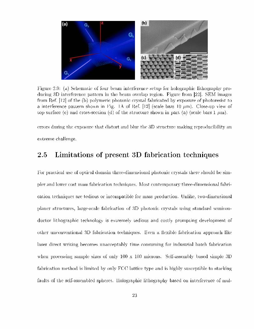
Figure 2.9: (a) Schematic of four beam interference setup for holographic lithography pro-ducing 3D interference pattern in the beam overlap region. Figure from [22]. SEM imagesfrom Ref. [12] of the (b) polymeric photonic crystal fabricated by exposure of photoresist toa interference pattern shown in Fig. 1A of Ref. [12] (scale bars 10 µm). Close-up view oftop surface (c) and cross-section (d) of the structure shown in part (a) (scale bars 1 µm).
errors during the exposure that distort and blur the 3D structure making reproducibility an
extreme challenge.
2.5 Limitations of present 3D fabrication techniques
For practical use of optical domain three-dimensional photonic crystals there should be sim-
pler and lower cost mass fabrication techniques. Most contemporary three-dimensional fabri-
cation techniques are tedious or incompatible for mass production. Unlike, two-dimensional
planer structures, large-scale fabrication of 3D photonic crystals using standard semicon-
ductor lithographic technology is extremely tedious and costly prompting development of
other unconventional 3D fabrication techniques. Even a �exible fabrication approach like
laser direct writing becomes unacceptably time consuming for industrial batch fabrication
when processing sample sizes of only 100 x 100 microns. Self-assembly based simple 3D
fabrication method is limited by only FCC lattice type and is highly susceptible to stacking
faults of the self-assembled spheres. Holographic lithography based on interference of mul-
23

tiple laser beams has, in part, met these criteria by providing a large variety of photonic
crystal templates in photo-sensitive materials. However, the inherent vibrational instability
problem of multiple beam holographic lithography introduces signi�cant phase and angle
errors during the exposure that distort and blur the 3D structure, making reproducibility
an extreme challenge.
In this context there is a need for development of some �exible 3D fabrication techniques
for high volume fabrication of 3D micro-nano structures. A di�ractive optical element (DOE)
is a promising alternative device for 3D lithography where one DOE creates multiple laser
beams in various di�raction orders that are inherently phase-locked and stable for repro-
ducible creation of 3D near-�eld di�raction patterns from a single laser beam. In this DOE
approach, control parameters such as grating period, duty cycle and laser wavelength de-
termine the periodic crystal structure while etch depth, laser intensity, polarization and
photoresist threshold de�ne the �lling fraction and motif that together enables a wide va-
riety of 3D photonic crystal structures to be formed. The concept behind 3D near-�eld
di�raction pattern is well known since mid eighteen hundreds [13]. Rogers and cowork-
ers [14] were �rst to demonstrate the formation of 3D periodic structures in photoresist
using two-level (binary) DOEs. However, they could only fabricate a single basis structure
with body-centred-tetragonal (BCT) symmetry as can be seen in Fig. 2.10.
In our group, Lin et al. extended DOEs to the fabrication of 3D �Woodpile�-type pho-
tonic crystal templates in photoresist by double exposures of orthogonal phasemasks or
one-dimensional DOEs (1D-DOE) [15]. However, imprecise alignment between two DOE
exposures prevents this method from reproducibly interlace two 2D structures and a single
exposure DOE method is therefore preferred for convenience and improved uniformity of the
24

Figure 2.10: Body-centred-tetragonal (BCT) symmetry structure fabricated using binary2D DOE. Inset (a)-(c) shows top view and inset-(b)-(d) shows cross-sectional SEM views.Figure from [14].
3D structures.
Figure 2.11: Scanning electron microscope image woodpile-type photonic crystal recordedin the SU-8 photoresist (a) top view of the photonic structure and (b) cross-section view ofthe photonic structure. Figure from [15].
In this thesis, we demonstrate improved fabrication precision and the �rst spectral char-
acterization of Woodpile-type photonic crystal templates formed by 1D-DOE based double
laser exposure method. Subsequently, more complex multi-level DOEs have been proposed
to fabricate diamond-like photonic crystal structures in a single laser exposure step. These
DOEs simplify the 3D fabrication process to a single optical element based approach where
crystal symmetry, lattice constants, crystal basis information are encoded in the DOE [35,36].
Finite di�erence time domain calculation of near-�eld di�raction patterns are corroborated
25

by de�nitive demonstrations of diamond-like woodpile structure inside the photoresist. Spe-
cial attention was given to reduce axial to lateral crystal axis ratio (c/a) so that stopbands
shift into the 1.25-1.65 µm telecom band.
26

Chapter 3
Three-dimensional di�ractive optics
lithography
3.1 Introduction
Di�ractive optics lithography is based on the near-�eld self-imaging e�ect of a periodic
di�ractive optical element (DOE). When a plane wave is transmitted through a periodic
di�ractive structure, the resulting wave front propagates in such a way that the light �eld
replicates the structure along the propagation direction at multiples of a certain de�ned
distance, known as the Talbot length. The main objective of di�ractive optics lithography
is to capture this 3D light intensity distribution inside a photosensitive material to fabricate
3D periodic structures or photonic crystals. By suitable design of the di�ractive optical
element, the 3D spatial light intensity distribution can be controlled to obtain desire lattice
constants, motif shapes and symmetry. The origins of this 3D light intensity distribution, the
conditions necessary for it to occur and the control of light distribution to di�erent patterns
are the subject of this chapter.
27
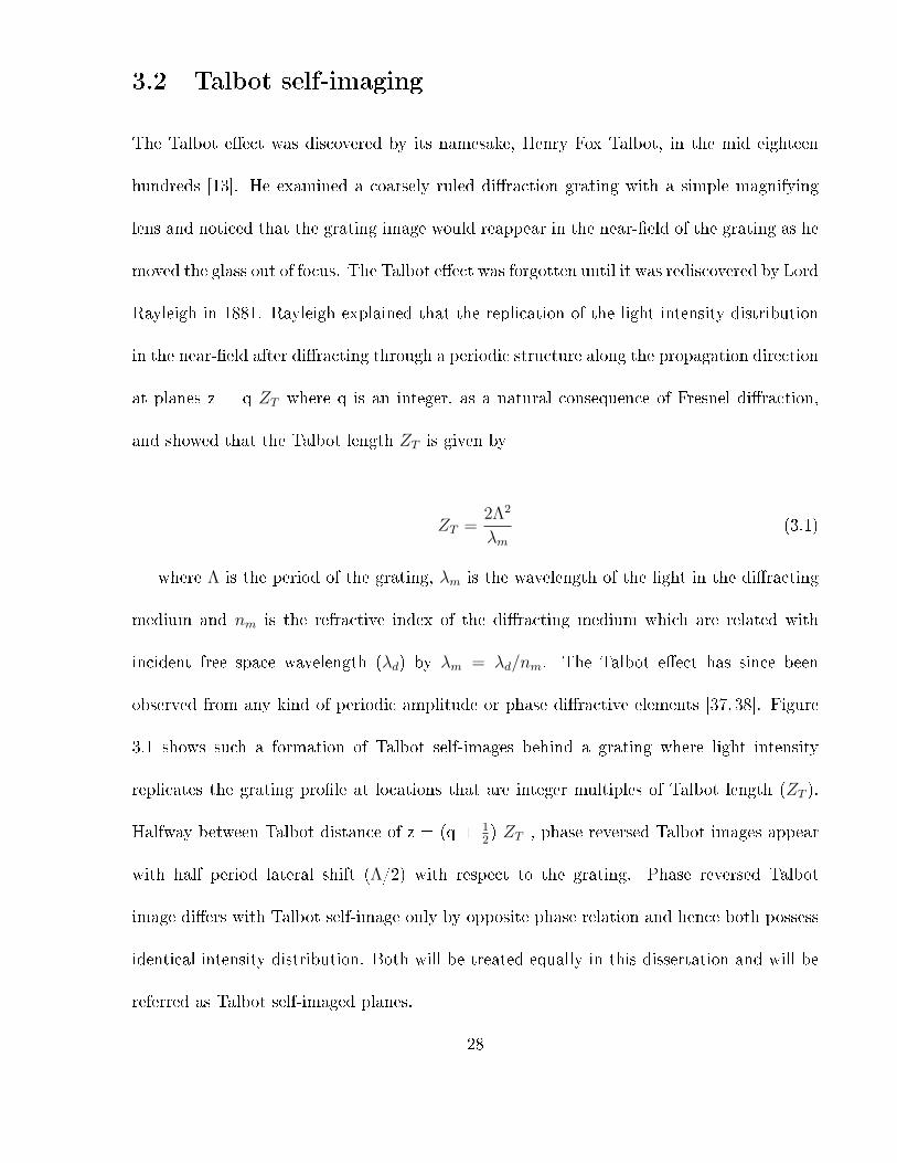
3.2 Talbot self-imaging
The Talbot e�ect was discovered by its namesake, Henry Fox Talbot, in the mid eighteen
hundreds [13]. He examined a coarsely ruled di�raction grating with a simple magnifying
lens and noticed that the grating image would reappear in the near-�eld of the grating as he
moved the glass out of focus. The Talbot e�ect was forgotten until it was rediscovered by Lord
Rayleigh in 1881. Rayleigh explained that the replication of the light intensity distribution
in the near-�eld after di�racting through a periodic structure along the propagation direction
at planes z = q ZT where q is an integer, as a natural consequence of Fresnel di�raction,
and showed that the Talbot length ZT is given by
ZT =2Λ2
λm(3.1)
where Λ is the period of the grating, λm is the wavelength of the light in the di�racting
medium and nm is the refractive index of the di�racting medium which are related with
incident free space wavelength (λd) by λm = λd/nm. The Talbot e�ect has since been
observed from any kind of periodic amplitude or phase di�ractive elements [37, 38]. Figure
3.1 shows such a formation of Talbot self-images behind a grating where light intensity
replicates the grating pro�le at locations that are integer multiples of Talbot length (ZT ).
Halfway between Talbot distance of z = (q + 12) ZT , phase reversed Talbot images appear
with half period lateral shift (Λ/2) with respect to the grating. Phase reversed Talbot
image di�ers with Talbot self-image only by opposite phase relation and hence both possess
identical intensity distribution. Both will be treated equally in this dissertation and will be
referred as Talbot self-imaged planes.
28
Figure 3.1: Locations of Talbot self-images behind a grating.
Interesting image formations also take place in certain fractional Talbot planes, located
between the planes z = (q + 12) ZT [37, 38]. This fractional Talbot imaging phenomenon
has been used in some interesting optical array illumination applications. However, in this
dissertation we will strictly restrict ourselves to Talbot self-images to fabricate 3D periodic
structures.
3.3 Arranging Talbot self-images into a photonic crystal
The Talbot self-imaging phenomenon can be observed in both amplitude and phase di�ractive
elements. However, only phase di�ractive elements are considered here due to advantages
of no energy loss as well as the possibility of di�raction control with multiple phase levels.
This formation of near-�eld periodic light intensity distribution behind a di�ractive optical
element looks attractive in fabricating photonic crystals. However, the challenge is to control
the periodic light intensity distribution so that it follows speci�c lattice constants, symmetry
29

and motif shape.
3.3.1 One-dimensional vs. two-dimensional di�ractive elements
An one-dimensional DOE creates 1D self-image of the grating which repeats along the optical
axis to form a 2D periodic pattern. A 2D DOE creates a 2D pattern which repeats along
the optical axis forming a 3D periodic intensity distribution. There are �ve distinct Bravais
lattices [23] for 2D periodic structures. However, in the present context we will only consider
the square lattice 2D DOE. Figure 3.2a shows the near-�eld di�raction patterns of a 1D DOE
forming a 2D log-like intensity distribution having lattice constants a and c. In contrast,
a 2D DOE creates a 3D periodic di�raction pattern having lattice constants a, b and c as
shown in Fig. 3.2b. However, for the Talbot self-imaging the DOE must produce at least
0th and ±1st di�racted beams [39]. This translationally symmetric arrangement of periodic
Talbot self-images can be classi�ed as a Bravais lattice. The lattice constants can be tuned
by controlling di�raction angles produced by the DOE. This periodic di�raction pattern
can be accurately captured inside a thick (� c) negative photoresist of refractive index nr
placed in the beam overlap region as shown in Fig. 3.2 and by applying a laser exposure that
just exceed the photo-polymerization threshold of the photoresist. However, a bi-continuous
3D intensity distribution is required for fabrication of stable 3D structures which does not
collapse after photoresist development. This depends on the inherent connectivity as well as
lattice constants of the intensity distribution.
3.3.2 De�ning lattice constants
It can be observed from Eq. 3.1 that for a given incident laser wavelength (λd) and photoresist
medium (nr), both lateral lattice constants a and b and the axial lattice constant c of the
30

Figure 3.2: Near-�eld di�raction pattern of a (a) grating or 1D-DOE and a (b) 2D DOEshowing a 2D log-like di�raction pattern and a 3D body-centred-tetragonal di�raction pat-terns respectively.
periodic intensity distribution can be controlled by suitable selection of DOE period (Λ).
Here, we assume that the 2D DOE period has equal periodicities of Λ1= Λ2= Λ resulting
in lateral lattice constant b = a which is a valid assumption for cubic or tetragonal crystal
symmetry groups and cases where b 6= a will be highlighted separately. A complete photonic
bandgap of photonic crystal structures is available only in a narrow range of cubic (c = a)
or near-cubic (c∼a) axial-to-transverse periodicity ratios, c/a, that further depends on the
refractive index of dielectric medium and the �lling fraction [22,24]. However, for fabrication
of cubic or near cubic crystals the ratio of the DOE period Λ and the laser wavelength in the
medium λm should be on the order of unity requiring large di�raction angles of di�racted
beam according to Eq. 3.2.
nm sin θm + nd sinφ =mλd
Λ(3.2)
where φ is angle of incidence, nd is refractive index of incident medium and θm is di�rac-
tion angle of m-th di�raction order.
31

Talbot self-imaging of periodic structures is well known to be a strictly paraxial phe-
nomenon. It was shown that the Talbot length (ZT ) departs signi�cantly from the its
classical form shown in Eq. 3.1 if the ratio of the grating period Λ and the laser wavelength
λd is of the order of ten, or less [38]. Assuming that only the three central di�raction orders
(m = -1, 0, 1) are propagating waves, i. e., 1 < Λ/λm ≤ 2, it has been demonstrated from
rigorous electromagnetic theory in [38] that for normal angle of incidence (φ = 0) the �eld
is always self-imaging for a generalized Talbot length given by:
ZTg =λm
1−√
[1− (λm/Λ)2](3.3)
This generalized Talbot self-imaging length has been derived from interference equations and
the complete derivation has been given in Appendix-A.
In this present research works the quest for fabricating cubic or near-cubic photonic
crystal lattices is far beyond the paraxial condition where only three central di�raction
orders (m = -1, 0, 1) are propagating waves. Hence, throughout this dissertation we will
be using the generalized Talbot length of Eq. 3.3 which reduces to classical Talbot length
of Eq. 3.1 for paraxial case of Λ/λm �1. A comparison of the classical and the generalized
Talbot length is presented in Fig. 3.3 which shows the variation of the ratio ZTg/ZT as a
function of normalized wavelength inside the photoresist medium (λm/Λ).
In this research work, a wavelength to period ratio of 0.5 <λm/Λ< 1 which necessitates
reassignment of axial lattice constant c to generalized Talbot length (ZTg) . The modi�ed
lattice constants are shown in Eq. 3.4.
a = Λ; c = ZTg =λm
1−√
[1− (λm/Λ)2](3.4)
32

Figure 3.3: Relation between generalized Talbot length (ZTg) and classical Talbot length(ZT ) as a function of normalized wavelength inside the photoresist medium (λm/Λ).
3.4 Determining depth of near-�eld
Due to �nite size of any practical di�ractive element and the large di�raction angles targeted
here, the length of beam overlap region or near-�eld is limited to an extremely short region
close to the di�ractive element. This has been termed the �walk-o�� e�ect in Talbot interfer-
ometry [39,40]. This is one of the drawback of using higher-order Talbot self-imaging planes
where di�racted beams gradually emerge as independent far-�eld beams. Hence, an accu-
rate estimation of this beam overlap region is essential in estimating appropriate photoresist
thickness and number of layers.
Figure 3.4 shows a ray-optics picture of far-�eld di�racted beams emerging from a DOE.
Except around the boundary of the beam overlap region, the ray-optics approach has been
found to accurately predict the central beam overlap region [39, 40]. Ray-optics approach
will be used here to establish a closed-form analytical formula to estimate this beam overlap
region. The hashed area in Fig. 3.4 shows a gradual narrowing of the conical shaped beam
overall region away from a grating DOE. Di�racted beams at two arbitrary distances of (a)
33

Figure 3.4: Ray-optics picture of di�racted beam walk-o� where K0, K±1 represent propa-gation vectors of 0th and ±1st order di�racted beams respectively.
Figure 3.5: Gradual narrowing of beam overlap region due to beam �walk-o�� of a gratingshown in Fig. 3.4 at arbitrary distances of (a) L1 and (b) L2 from grating surface as shownin Fig. 3.4.
L1 and (b) L2 away from the grating has been shown in Fig. 3.5. Here we can clearly observe
as we move away from the grating the beam overlap region reduces and gradually far-�eld
di�racted beams emerge with no mutual overlap between them.
The beam overlap region or near-�eld volume depends on period of the di�ractive element
(Λ) as well as on laser wavelength inside the medium (λm). Figure 3.6 shows beam overlap
regions of di�raction from normally illuminated (λd = 514 nm) (a) 1D-DOE or phasemask of
period Λ = 650 nm and (b) 2D-DOE of period Λx = Λy = Λ = 650 nm where the 1D-DOE
34

Figure 3.6: Estimation of beam overlap region of (a) di�raction from a normally illuminated1D-DOE and (b) normally illuminated 2D-DOE.
created 3 di�racted beams of (0,0), (1,0), (-1,0) order and the 2D-DOE created 5 di�racted
beams of (0,0), (1,0), (-1,0),(0,1),(0,-1) where (m, n) represents order of a di�racted beam. To
estimate the beam overlap region it has been assumed that the DOE is normally illuminated
with a �at-top beam of radius R. In Fig. 3.6, Wx and Wy represents two radii of beam
overlap region along X and Y axis and P represents beam walk-o� length at a given distance
from the DOE. Following the di�raction angle equation of Eq. (3.2) and Snell's law, the
beam walk o� length is:
P =N∑m=1
Lm tan(sin−1(λdnmΛ
)) (3.5)
where Lm is propagation distance in each medium, N represents number of di�erent
medium between DOE and the plane of observation and nm is the corresponding refractive
index of each medium. The corresponding beam overlap radius is given by:
W = (R− P ) ;∀P ≤ R; ∀W = min(Wx,Wy) (3.6)
The depth of near-�eld can be estimated using Eq. (3.5) and Eq. (3.6) for a given beam
overlap radius (W ) to incident beam radius (R) ratio of r = W/R inside a medium (nN):
35

dnf (r, nN) =
(1− r)R−N−1∑m=1
Lm tan(sin−1( λd
nmΛ))
tan(sin−1(λdnN Λ
)); ∀dnf (r, nN) ≥ 0; 0 ≤ r ≤ 1; (3.7)
where nN is the refractive index of the recording medium where the near-�eld depth
dnf (r, nN) is de�ned and n1....nN−1 and L1....LN−1 represent refractive indices and thick-
nesses of (N − 1) media layers preceding the medium of observation (nN). According to Fig.
3.4 the near-�eld depth dnf (r, nr) = Lr inside the photoresist layer (nr) for a given beam
overlap ratio of r = W/R = 0.5. It can be guessed from Eq. 3.7 that to obtain a higher
beam overlap ratio (r = W/R) the laser wavelength to DOE period ratio (λd/Λ) needs to
be restricted to a lower value. However, as mentioned in Section 3.3.2 to achieve lower c/a
ratio of the fabricated structure, laser wavelength to DOE period ratio (λd/Λ) needs to be
higher. This contradictory requirement requires special attention during DOE design.
3.5 Simulation of near-�eld intensity distribution
Simulation of the near-�eld di�raction pattern plays a key role in designing a di�ractive
optical element for 3D lithography. On one hand, the simulated intensity distribution helps
in optimizing fabrication process and enables band calculation which in turn guides optical
characterization of the fabricated structure. The band and intensity distribution calculation
needs to be iteratively optimized for the �nal design of a di�ractive optical element. The
near-�eld di�raction pattern calculation starts with di�raction e�ciency calculations and
follows with interference intensity distribution and 3D isointensity surface generation.
36

3.5.1 Di�raction e�ciency calculation
Di�raction e�ciency of a DOE can be calculated by solving scalar or vector wave equations.
However, in the present research where we always work in the non-paraxial regime (λ∼Λ),
full-vectorial calculation is required for accurate di�raction e�ciency prediction [41]. There
are two major full-vectorial di�raction e�ciency calculation methods. One is Rigorous Cou-
pled Wave Analysis (RCWA) [42] and another one is FDTD. However, it is well known that
the RCWA predictions of di�raction e�ciency is more accurate than FDTD predictions [41]
and hence throughout this research work di�raction e�ciency has been calculated using a
RCWA based commercial algorithm GSolver (GSolver Inc.). The software uses a unit cell
phase pro�le of a DOE to calculate di�raction e�ciencies of di�erent di�racted beams for a
given laser wavelength, polarization and angle of incidence. The di�raction e�ciency (ηmn)
of (m,n)th di�raction order is de�ned by:
ηmn =PmnPin
=DiD
∗i
Pin(3.8)
where Pmn is the power of (m,n)th di�raction order, Di is the corresponding amplitude
of the di�raction order and Pin is the incident power on the DOE. To illustrate calculation of
di�raction e�ciency, a 1D-DOE or phasemask of period Λ = 650 nm, DOE refractive index
nd = 1.46 and background refractive index nb = 1.0 has been chosen for the arrangement Fig.
3.7. The mask has been illuminated normally with TM polarized laser light of wavelength
λd = 514 nm where TM polarization is de�ned as polarization vector parallel to the grating
grooves.
According to the di�raction angle equation Eq. (3.2), the DOE creates (0, 0), (1, 0) and
(−1, 0) order di�racted beams as shown in Fig. 3.7. The di�raction e�ciency of 0th and 1st
37
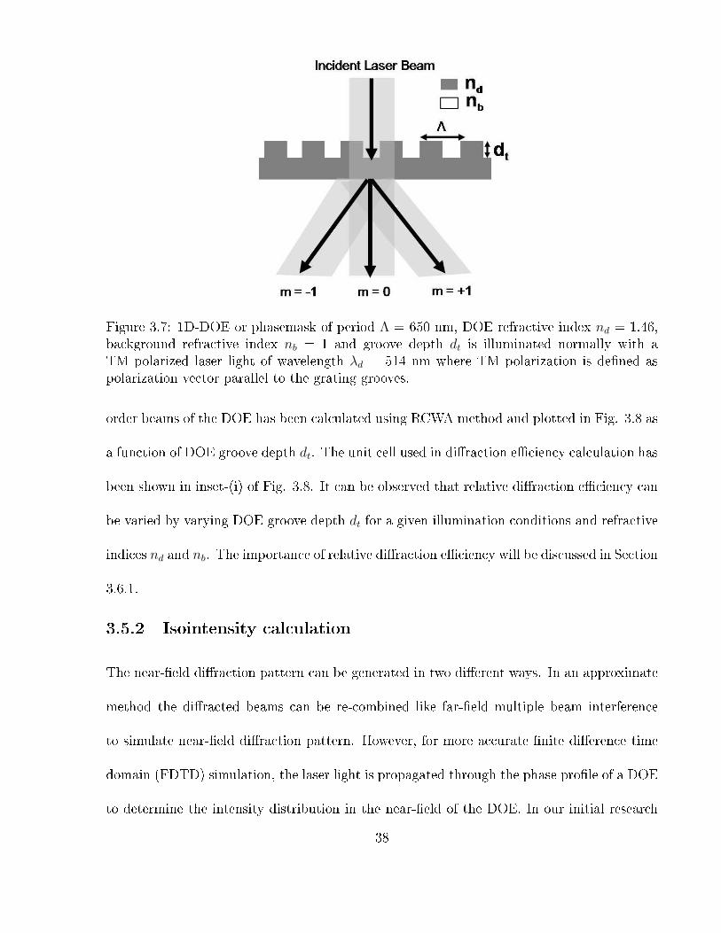
Figure 3.7: 1D-DOE or phasemask of period Λ = 650 nm, DOE refractive index nd = 1.46,background refractive index nb = 1 and groove depth dt is illuminated normally with aTM polarized laser light of wavelength λd = 514 nm where TM polarization is de�ned aspolarization vector parallel to the grating grooves.
order beams of the DOE has been calculated using RCWA method and plotted in Fig. 3.8 as
a function of DOE groove depth dt. The unit cell used in di�raction e�ciency calculation has
been shown in inset-(i) of Fig. 3.8. It can be observed that relative di�raction e�ciency can
be varied by varying DOE groove depth dt for a given illumination conditions and refractive
indices nd and nb. The importance of relative di�raction e�ciency will be discussed in Section
3.6.1.
3.5.2 Isointensity calculation
The near-�eld di�raction pattern can be generated in two di�erent ways. In an approximate
method the di�racted beams can be re-combined like far-�eld multiple beam interference
to simulate near-�eld di�raction pattern. However, for more accurate �nite di�erence time
domain (FDTD) simulation, the laser light is propagated through the phase pro�le of a DOE
to determine the intensity distribution in the near-�eld of the DOE. In our initial research
38

Figure 3.8: Di�raction e�ciency of the 1D-DOE shown in Fig. 3.7 as a function of DOEgroove depth dt for DOE period Λ = 650 nm, DOE refractive index nd = 1.46 and backgroundrefractive index nb = 1.0. The DOE has been illuminated normally with TM polarized laserlight of wavelength λd = 514 nm. Inset-(i) shows the unit cell used in di�raction e�ciencycalculation.
work we have used far-�eld interference for approximate predictions of near-�eld di�raction
pattern and then moved to FDTD based exact near-�eld calculations for our later device
demonstrations.
3.5.2.1 Interference equation based beam re-combination method
In di�ractive optics lithography where the di�raction pattern is captured inside a photo-
sensitive material using a step-function like response of the photo-sensitive material, less
accurate far-�eld interference predictions have shown to match the contours of fabricated
structures inside photo-sensitive materials [14,43]. In far-�eld calculation, parabolic or spher-
ical wavefronts of near-�eld di�racted beams is approximated with plane wave wavefronts
and each di�racted beam is treated as an independent monochromatic plane wave. The
interference of N such di�racted beams of frequency ω, propagation vector Ki, polarization
39

vector εi and di�raction amplitude Di creates a �eld given by:
E(r , t) = e−jωtN−1∑i=0
Di εiej(Ki.r+φi) (3.9)
where the propagation vector Ki is de�ned by di�raction angle and laser wavelength
and φi is relative phase of di�racted beams. The di�raction amplitude Di is related to the
incident power (Pin) through the di�raction e�ciency (ηmn) as given in Eq. (3.8). The
stationary intensity pattern produced by the interference described above is given by:
I(r) = E∗(r , t) · E(r , t) =
N−1∑i=0
D2i + 2[
N−1∑i=1
D0Diε0.εicos((Ki −K0).r + (φi − φ0)) (3.10)
+N−1∑i>j=1
DiDjεi.εjcos((Ki −Kj).r + (φi − φj))] = I0 + 24I(r)
where I0 is the average background intensity and 4I is the position dependent variation
of intensity. The calculated intensity distribution is passed through a step-function threshold
(Ith) to closely mimic the photoresist response, yielding the 3D isointensity distribution. By
convention we consider that the high intensity regions in Eq. (3.10) will become the high
dielectric component of the photonic crystal (ε(r̄) = 1 where I(r̄) < Ithand ε(r̄) > 1 where
I(r̄) ≥ Ith).
3.5.2.2 Finite di�erence time domain method
The complex near-�eld di�raction pattern has been extensively studied by many researchers
using scalar di�raction theory [44]. The scalar di�raction theory possesses closed form an-
alytical expression and hence is relatively simple to use in predicting near-�eld di�raction
patterns. Unlike scalar theory, there is no closed form analytical expression for calculating
near-�eld di�raction with a full vectorial approach. Hence, one needs discrete numerical
40
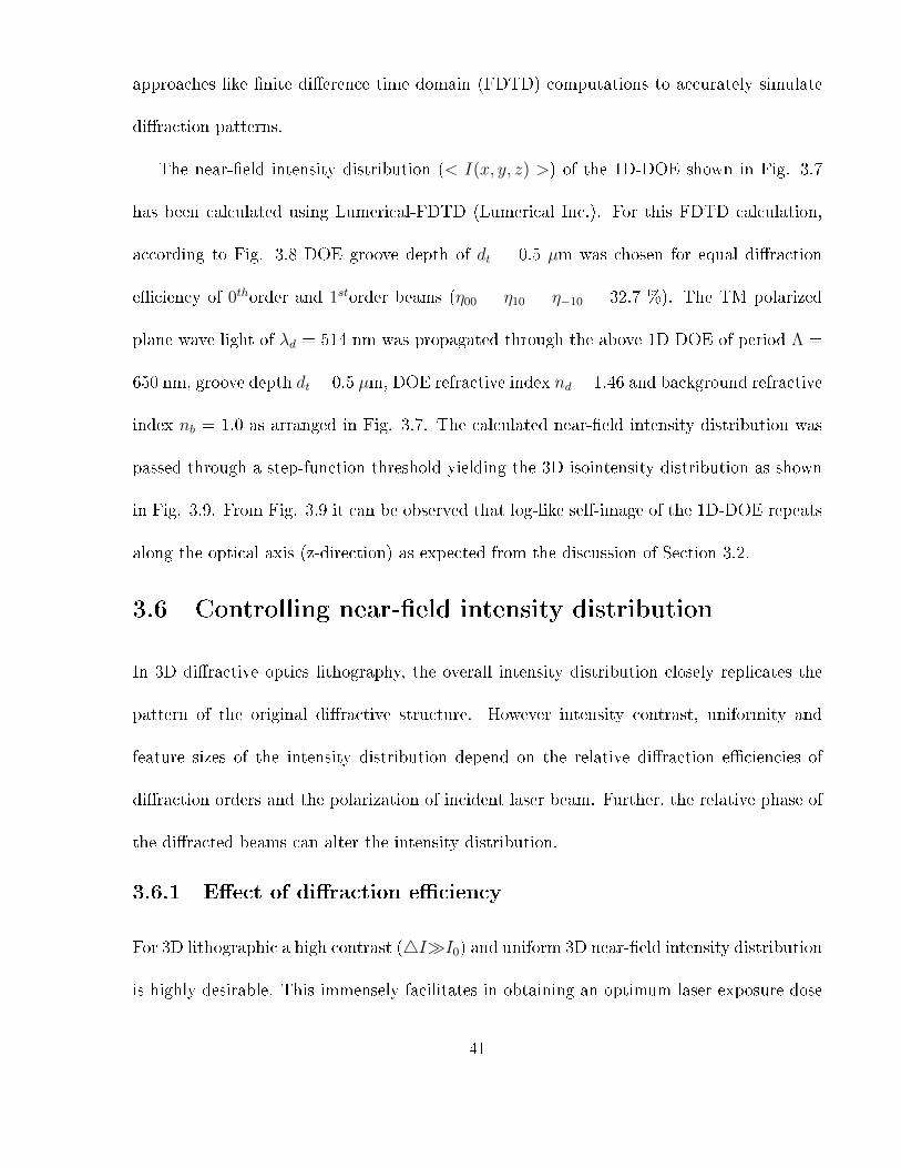
approaches like �nite di�erence time domain (FDTD) computations to accurately simulate
di�raction patterns.
The near-�eld intensity distribution (< I(x, y, z) >) of the 1D-DOE shown in Fig. 3.7
has been calculated using Lumerical-FDTD (Lumerical Inc.). For this FDTD calculation,
according to Fig. 3.8 DOE groove depth of dt = 0.5 µm was chosen for equal di�raction
e�ciency of 0thorder and 1storder beams (η00 = η10 = η−10 = 32.7 %). The TM polarized
plane wave light of λd = 514 nm was propagated through the above 1D DOE of period Λ =
650 nm, groove depth dt = 0.5 µm, DOE refractive index nd = 1.46 and background refractive
index nb = 1.0 as arranged in Fig. 3.7. The calculated near-�eld intensity distribution was
passed through a step-function threshold yielding the 3D isointensity distribution as shown
in Fig. 3.9. From Fig. 3.9 it can be observed that log-like self-image of the 1D-DOE repeats
along the optical axis (z-direction) as expected from the discussion of Section 3.2.
3.6 Controlling near-�eld intensity distribution
In 3D di�ractive optics lithography, the overall intensity distribution closely replicates the
pattern of the original di�ractive structure. However intensity contrast, uniformity and
feature sizes of the intensity distribution depend on the relative di�raction e�ciencies of
di�raction orders and the polarization of incident laser beam. Further, the relative phase of
the di�racted beams can alter the intensity distribution.
3.6.1 E�ect of di�raction e�ciency
For 3D lithographic a high contrast (4I�I0) and uniform 3D near-�eld intensity distribution
is highly desirable. This immensely facilitates in obtaining an optimum laser exposure dose
41

Figure 3.9: FDTD calculation of isointensity surface of the near-�eld di�raction patternof the 1D-DOE shown in Fig. 3.7 for normal incident TM polarized plane wave light ofwavelength λd = 514 nm.
as well as a wider exposure window to optimize �lling fraction (ff) of the 3D structure. The
intensity contrast is de�ned as:
C =Imax − IminImax + Imin
(3.11)
From Eq. (3.9) it is evident that the intensity contrast depends on relative amplitudes
(Di) of the di�racted beams (i.e. di�raction e�ciency). To illustrate the inter relation
between intensity contrast and relative di�raction e�ciency, a near-�eld di�raction pattern
of the DOE shown in Fig. 3.7 has been calculated using FDTD for same set of parameters
used in the di�raction e�ciency calculation in Fig. 3.8. A TM polarized plane wave light
of wavelength λd = 514 nm has been propagated through the 1D-DOE shown in Fig. 3.7
for varying groove depth dt between the range 0.47 µm - 0.1 µm, which according to Fig.
42

3.8 corresponds to the range of 0th to 1th order di�raction e�ciency ratio of η0/η1 = 0.58
- 20 for constant DOE refractive index nd = 1.46 and background refractive index nb =
1.0. The variation of intensity contrast (C) with the di�raction e�ciency ratio (η0/η1)
is shown in Fig. 3.10. It can be observed from Fig. 3.10 that the intensity contrast is
insensitive to relative di�raction e�ciency of 0th order and 1st order di�racted beams for a
relatively large di�raction e�ciency ratio of η0/η1≈ 1 to 6 which means each of ±1st order
beams should possess at least ≈ 12.5% di�raction e�ciency in order to maintain maximum
intensity contrast of C = 1. This point highlights the importance of accurate di�raction
e�ciency estimation in DOE design for creating high contrast intensity distribution. This is
essential in di�ractive optics lithography for precise control of laser exposure dose to obtain
a structure with a desired �lling fraction.
3.6.2 E�ect of polarization
Di�raction e�ciency of a phase only di�ractive structure primarily depends on phase depth.
It is generally believed that di�raction e�ciency doesn't depend on polarization of incident
light. However, for non-paraxial case (Λ∼λ) it has been found that di�raction e�ciency is
also a function of polarization of incident light [38].
3.6.2.1 E�ect on di�raction e�ciency and intensity contrast
To understand the e�ect of polarization, the di�raction e�ciency of the same 1D-DOE or
phasemask shown in Fig. 3.7 has been calculated for TE, TM and circularly polarized light
by the RCWA method. The same DOE parameters of period Λ = 650 nm, DOE refractive
index nd = 1.46 , background refractive index nb = 1.0 and laser wavelength of λd = 514
nm have been used. The laser wavelength λd = 514 nm and phasemask period Λ = 650 nm
43

Figure 3.10: Variation of intensity contrast (C) with 0thorder to 1storder di�raction e�ciencyratio (η0/η1) of the near-�eld intensity distribution of the 1D-DOE shown in Fig. 3.7 for sameset of parameters used in the di�raction e�ciency calculation in Fig. 3.8. The di�ractione�ciency ratio η0/η1 = 0.58 - 20 of RCWA based di�raction e�ciency prediction correspondsto DOE groove depth dt between the range 0.47 µm - 0.1 µm.
have been chosen speci�cally to satisfy the non-paraxial condition. Results for 0th and 1st
order beams are shown in Fig. 3.11 as a function of DOE groove depth dt.
From Fig. 3.11 it can be observed that di�raction e�ciency depends on polarization
of the incident laser beam. For a given groove depth (dt) di�raction e�ciency of TE and
TM polarized light di�ers by up to 25%. As expected, di�raction e�ciency of circularly
polarized light is halfway between that for TE and TM polarized light. The corresponding
variation of intensity contrast (C) with di�raction e�ciency ratio (η0/η1) is shown in Fig.
3.12 for all three polarizations. It can be observed that unlike TM polarization, intensity
contrast strongly depends on η0/η1 ratio for TE and circular polarizations. This shows the
importance of polarization in obtaining desired di�raction e�ciencies of a given DOE and
44
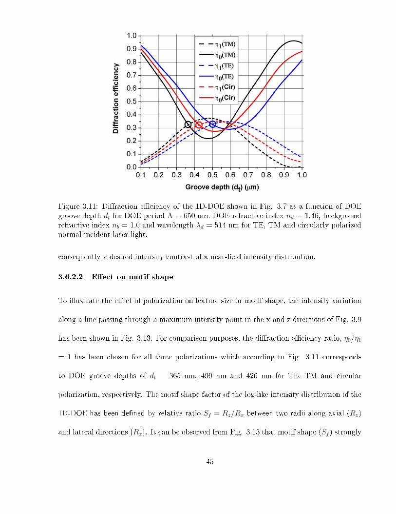
Figure 3.11: Di�raction e�ciency of the 1D-DOE shown in Fig. 3.7 as a function of DOEgroove depth dt for DOE period Λ = 650 nm, DOE refractive index nd = 1.46, backgroundrefractive index nb = 1.0 and wavelength λd = 514 nm for TE, TM and circularly polarizednormal incident laser light.
consequently a desired intensity contrast of a near-�eld intensity distribution.
3.6.2.2 E�ect on motif shape
To illustrate the e�ect of polarization on feature size or motif shape, the intensity variation
along a line passing through a maximum intensity point in the x and z directions of Fig. 3.9
has been shown in Fig. 3.13. For comparison purposes, the di�raction e�ciency ratio, η0/η1
= 1 has been chosen for all three polarizations which according to Fig. 3.11 corresponds
to DOE groove depths of dt = 365 nm, 499 nm and 426 nm for TE, TM and circular
polarization, respectively. The motif shape factor of the log-like intensity distribution of the
1D-DOE has been de�ned by relative ratio Sf = Rz/Rx between two radii along axial (Rz)
and lateral directions (Rx). It can be observed from Fig. 3.13 that motif shape (Sf ) strongly
45
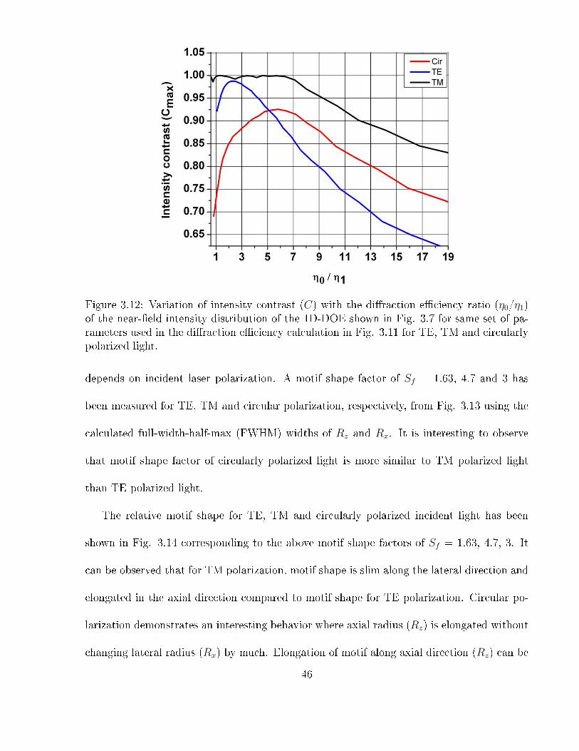
Figure 3.12: Variation of intensity contrast (C) with the di�raction e�ciency ratio (η0/η1)of the near-�eld intensity distribution of the 1D-DOE shown in Fig. 3.7 for same set of pa-rameters used in the di�raction e�ciency calculation in Fig. 3.11 for TE, TM and circularlypolarized light.
depends on incident laser polarization. A motif shape factor of Sf = 1.63, 4.7 and 3 has
been measured for TE, TM and circular polarization, respectively, from Fig. 3.13 using the
calculated full-width-half-max (FWHM) widths of Rz and Rx. It is interesting to observe
that motif shape factor of circularly polarized light is more similar to TM polarized light
than TE polarized light.
The relative motif shape for TE, TM and circularly polarized incident light has been
shown in Fig. 3.14 corresponding to the above motif shape factors of Sf = 1.63, 4.7, 3. It
can be observed that for TM polarization, motif shape is slim along the lateral direction and
elongated in the axial direction compared to motif shape for TE polarization. Circular po-
larization demonstrates an interesting behavior where axial radius (Rz) is elongated without
changing lateral radius (Rx) by much. Elongation of motif along axial direction (Rz) can be
46

Figure 3.13: Intensity variation across a line (a) in the x and (b) in the z directions of Fig.3.9 passing through the maximum intensity point in the respective directions calculated byFDTD.
useful for establishing connection between two adjacent layers in the axial direction to form
a stable interconnected 3D structure [43].
The motif shape factor plays an important role in controlling �lling fraction with laser
exposure dose. Figure 3.15 shows change of �lling fraction with laser exposure dose of the
same intensity distribution shown in Fig. 3.9. The laser exposure dose has been normalized
with the maximum intensity of three intensity distributions corresponding to three polariza-
tions. It can be observed from Fig. 3.15 that for a given laser exposure dose TE, TM and
circular polarization creates intensity distribution with three di�erent �lling fractions. The
slope of change of �lling fraction curve dictates the sensitivity of laser exposure dose control
in obtaining a given �lling fraction for a given polarization. Hence, selecting a proper polar-
ization for a given DOE design is very important for fabrication of high quality reproducible
3D structures.
47

Figure 3.14: Relative motif shape of the intensity distribution shown in Fig. 3.9 correspond-ing to motif shape factor Sf = 1.63, 4.7 and 3 for TE, TM and circularly polarized light,respectively, for a constant di�raction e�ciency ratio η0/η1 = 1 for all three polarization.
3.6.3 E�ect of relative phase of di�racted beams
It is evident from Eq. (3.10) that the interference pattern depends on the relative phase
(φi) of the interfering beams. Relative phase between interfering beams has been shown
to change interference pattern by inserting delay elements in one or more beam paths in
multi-beam interference [45]. Similar e�ects have been demonstrated in cross-grating based
far-�eld interference as well [46]. However, unlike multi-beam holography, relative phase
control of di�racted beams is not possible in near-�eld di�ractive optic lithography. Since
all di�racted beams are phase locked with respect to the di�racting surface.
In the present research work we propose a phase-tunable DOE with multiple surfaces
which enabled tuning of phase di�erence of one set of �rst order di�racted beams with the
physical separation between the two di�ractive elements which enabled fabrication of contin-
uum of di�erent 3D periodic structures that are tunable from the double basis diamond-like
structure to a single basis structure having body-centered-tetragonal symmetry (BCT). Fur-
48
Figure 3.15: Change of �lling fraction as a function of exposure dose of the intensity distri-bution shown in Fig. 3.9.
ther, we propose a single-surface multi-level DOE with locked-in phase shift to enable fabri-
cation of a wide range of 3D structures. These phase control mechanisms will be elaborated
in subsequent chapters.
3.7 Photonic band calculation
Band calculation plays the most important part in characterizing any periodic structure.
There are number of di�erent techniques for band calculations of electronic crystals, however
band structures of photonic crystals have almost exclusively been obtained from the plane
wave expansion (PWE) method [20]. This is a well known concept of solving Maxwell's
equations for any spatially periodic structures. Unlike electronic crystals, the �periodic
potentials� in photonic bandgap materials are known and do not need to be computed in a
self-consistent fashions like electronic crystals.
49

3.7.1 Plane wave expansion theory
The PWE method is based on the Bloch-Floquet theorem, which states that Eigen solutions
of di�erential equations with periodic coe�cients may be expressed as a product of plane
waves and lattice-periodic functions. Consequently, all periodic functions are expanded into
appropriate Fourier series. Inserting these expansions into the Maxwell's equations results
in a large matrix-eigenvalue problem, which after suitable truncation, provides the Eigen
frequencies and expansion coe�cients for the Eigen function [20].
We start with vector wave equations for displacement �eld, D.
∇×∇× D(r)
ε(r)=ω2
c2D(r) (3.12)
The periodic dielectric constant de�nes a three-dimensional lattice and corresponding three-
dimensional reciprocal lattice vectors de�ned by κ(r) = 1/ε(r). Using the Bloch theorem
and Fourier expansion, D(r) and κ(r) can be written as:
D(r) = d(r) eikr =∑G
dGeiGreikr =
∑G
dGei(k+G)r (3.13)
κ(r) =∑G
κGeiGr (3.14)
where G is the reciprocal lattice vector of the periodic structure. By substituting Eq. (3.13)
and Eq. (3.14) into Eq. (3.12), we get
∇×∇× (∑G1G2
κG2dG1
ei(k+G1+G2)r) =ω2k
c2
∑G
dGei(k+G)r) (3.15)
The divergence-free electric �eld permits an expansion of the form
50
Dk =∑G
∑λ
wλGSλ
G ei(k+G)r (3.16)
where Sλ
G, λ= 1, 2 denote two unit vectors such that the set {Sλ=1
G , Sλ=2
G , (k+G)} forms an
orthogonal triad. The matrix-eigenvalue equation corresponding to Eq. (3.15) then becomes
∑G
∑G
′
κG−G′ |k +G||k +G′|(S
1
GS1
G′
S2
GS1
G′
S1
GS2
G′
S2
GS2
G′)(w1
G′
w2
G′
) =ω2k
c2(w1G
w2G
) (3.17)
where {wλ=1G
, wλ=2G
} are eigen vectors corresponding to the E or H �eld. Again, following
Ref. [20], instead of computing the Fourier coe�cients κG−G′ directly from Eq. (3.14), we
compute the matrix εG−G′ of Fourier coe�cients of ε(r) for the set of reciprocal lattice vectors
that de�ne the matrix in Eq. (3.17). We then take κG−G′ to be the (G, G′) element of the
inverse of the matrix εG−G′ . This procedure is known to dramatically improve the convergence
of eigenvalue computations [29, 47, 48]. Regular geometrical shapes like circle, rectangle,
sphere and cylinder possess closed form analytical expression for Fourier coe�cient εG−G′
and hence it is straight forward to solve Eq. (3.17) to obtain the band dispersion relation
of structures made of these fundamental motifs. However, structure made of irregular motif
does not possess a closed form expression for εG−G′ and hence need numerical techniques to
solve Eq. (3.17) for such structures.
3.7.2 Numerical plane wave expansion of periodic structures
The periodic structures made of highly convoluted shapes that do not conform to any typi-
cally known regular geometrical shapes and therefore preclude the use of analytic approaches
for the plane wave expansion method to accurately generate the band-dispersion curves.
However, with numerical techniques, bands of any arbitrary shape periodic structure can be
51

computed accurately as discussed in this section.
3.7.2.1 Discrete representation and classi�cation of the 3D periodic structures
For numerical band calculation, the isointensity surface computed following methods Section
3.5.2 is decomposed into a �ne mesh grid where each grid point represents the relative
permittivity of the material at that point. Selection of appropriate spatial sampling frequency
of the 3-dimensional mesh is critical for the accuracy of the PWE method. Overly coarse
meshing of the structure leads to signi�cant aliasing errors in the band calculation. In some
cases irregular motifs make it di�cult to estimate the appropriate spatial frequency of the
structure. In those cases aliasing errors can be avoided by selecting a large number of mesh
points. However, structures with highly convoluted features also require low pass �ltering to
avoid sampling anomalies in numerical band calculation.
The observed structure is �rst classi�ed amongst the 14 known Bravais lattices [23] in
order to identify reciprocal lattice vectors (G) which best represent the symmetry of the
structure. Due to highly convoluted shapes of these structures, this classi�cation process
is cumbersome. Inspection of such a structure does not immediately reveal its symmetry
and requires cross-sectional views of various planes to be plotted as mentioned in [49]. This
principle of identifying the Bravais lattice symmetry can be extended to any 3D periodic
structure which simply requires that appropriately spaced cross-sectional views be examined
that reveal the structural periodicity along the x, y and z directions.
3.7.2.2 Numerical representation of plane wave expansion
To solve Eq. (3.17) numerically, reciprocal lattice vectors (G), Fourier coe�cients κG−G′ of
the structure and orthogonal vectors {Sλ=1
G , Sλ=2
G } have to be obtained for each scan point
52

(k) along the Brillouin zone of the Bravais lattice of the structure.
A. Scanning along the irreducible Brillouin zone
To solve the Eigen values of the matrix formed by Eq. (3.17), a k-space needs to be selected
over which the bandgap of the structure is probed. It is well known from semiconductor
physics that to accomplish this purpose it is su�cient to choose k from the irreducible
Brillouin zone of the reciprocal structure [23]. Moreover, to save computation time, only
scan paths along high symmetry points of the irreducible Brillouin zone can be probed for
the band calculation because only at the boundaries of the Brillouin zone Bragg di�raction
condition is satis�ed which enhances the possibility of opening up of the bandgap at that
point on the k-space.
B. Finding lattice constants of the discretized structure
Both real and reciprocal lattice constants of a periodic structure should be known for plane
wave expansion of the structure. If we assume that a 3-dimensional structure possesses Px
period in x-direction, Py period in y-direction and Pz period in z-direction. Then the discrete
domain lengths of the unit cell in x, y, z directions are a′x = Nx
Px, a′y = Ny
Py, a′z = Nz
Pz, where
Nx, Ny and Nz are the number of samples of the discrete structure in the x, y, z directions,
respectively. Hence, normalized lengths of the unit cell in x, y, z directions are ax =a′xa, ay
=a′ya, az =
a′zawhere a = min{a′x,a
′y,a′z}. Now depending on the particular lattice symmetry,
primitive lattice constants of the real space are derived as function of ax, ay and az. For
example, Tetragonal (TTR) primitive lattice constants are a1= [ax, 0, 0], a2= [0, ay, 0] and
a3= [0, 0, az]. From primitive lattice constants of the real space, lattice constants for the
reciprocal space can be obtained as:
53
b1 = 2πa2 × a3
a1·a2 × a3
, b2 = 2πa1 × a3
a2·a1 × a3
, b3 = 2πa1 × a2
a3·a1 × a2
(3.18)
From the classi�cation of the 3-dimensional periodic structure according to one of the
14 Bravais lattices, the primitive ({a1, a2, a3}) and reciprocal ({b1, b2, b3}) lattice constants
are obtained as described above. The reciprocal lattice vectors (G) are formed as G =
s1b1+ s2b2 + s3b3 where s1, s2, s3 are integers. In plane wave expansion method these G
are considered as plane waves. For accurate band calculation G should span a symmetric
3-dimensional volume like a sphere or cube in the reciprocal space of the lattice. Ideally, an
in�nite number of plane waves (G) are needed for accurate band calculation. However, for
all practical purposes, the band diagram obtained with su�ciently large number of plane
waves (G) converge accurately. The dependence of band calculation accuracy on number of
plane waves is shown in Section 3.7.3.1.
C. Finding orthogonal unit vectors
In Eq. (3.17), Sλ
Gλ=1,2 denote two unit vectors such that the set {Sλ=1
G , Sλ=2
G , (k+G)} forms
an orthogonal triad. That means for each scan point (k) and for each reciprocal lattice vector
(G), two mutually orthogonal unit vectors which are normal to k+ G, need to be de�ned.
This can be accomplished as [50]:
Zk+G =k +G
|(k +G)|; S
1
G =(k +G)× A|(k +G)× A|
; S2
G = Zk+G × S1
G (3.19)
where A is an arbitrary vector which is not parallel to (k + G).
54
D. Fourier expansion of the discrete structure
To solve the eigenvalue Eq. (3.17), one requires the Fourier coe�cients κG−G′ . Again,
as stated in Section 3.7.1, instead of computing the Fourier coe�cients directly from Eq.
(3.14), we compute the matrix εG−G′ of Fourier coe�cients of ε(r) for the set of reciprocal
lattice vectors that de�ne the matrix in Eq. (3.17). A fast Fourier transform is used as the
mathematical tool to expand the 3-dimensional periodic structure (ε(x, y, z) ) in terms of
plane waves.
ε(fx, fy, fz) =Nx−1∑mx=0
Ny−1∑my=0
Nz−1∑mz=0
ε(x, y, z) e−i(
2π
Nx
mxkx+2π
Ny
myky+2π
Nz
mzkz)
(3.20)
where mx = 0, 1, ....(Nx − 1), my = 0, 1, ....(Ny − 1), mz = 0, 1, ....(Nz − 1) and kx =
0, 1, ....(Nx − 1), ky = 0, 1, ....(Ny − 1), kz = 0, 1, ....(Nz − 1). Nx, Ny, Nzare lengths of the
structure in x, y, z directions respectively. In the Fourier transform, the discrete plane wave
frequency bins are:
fx =2π
Nx
kx , fy =2π
Ny
ky , fz =2π
Nz
kz (3.21)
The matrix ε(fx, fy, fz) contains plane wave expansion coe�cients for all frequency bins
ranging between 0 to2π
Ns
(Ns − 1) for s = x, y and z. However, to solve the eigenvalue
Eq. (3.17), the PWE coe�cients for frequency bins at previously speci�ed reciprocal lattice
vectors (G-G′) are needed. Hence, we need to establish a relation between ε(fx, fy, fz) and
ε(G−G′). Careful observation reveals that
Gx −G′x =2π
axagx =
2π
Nx
Pxgx, gx ∈ R; Gy −G′y =2π
ayagy =
2π
Ny
Pygy, gy ∈ R; (3.22)
Gz −G′z =2π
azagz =
2π
Nz
Pzgz, gz ∈ R
55

Now by comparing Eq. (3.21) and Eq. (3.22), it can be observed that kx = Pxgx,
ky = Pygy and kz = Pzgz. For a chosen (G-G′) in Eq. (3.17), the integers gx, gy, gz
are known from Eq. (3.22). Hence, plane wave expansion coe�cients can be chosen as
ε(G − G′)=ε(fx, fy, fz) = ε(Pxgx, Pygy, Pzgz). Due to periodicity of the Fourier transform,
we need to make changes to the frequency bins as:
ks = Psgs; ∀0 ≤ Psgs ≤ (Ns − 1)
ks = Psgs −Ns; ∀Psgs > (Ns − 1); s = x, y, z; (3.23)
ks = Psgs +Ns; ∀Psgs < 0
In this way, the ε(G−G′) matrix can be formed from the discrete Fourier transformation
of the material mesh (ε(fx, fy, fz)). Now, inversion of the matrix ε(G − G′) will give us
κ(G−G′) as required to solve Eq. (3.17).
3.7.3 Band calculation of 3D periodic structures
The accuracy of the numerical PWE method has been tested here against well accepted band
calculations for several structures with simple regular geometrical motifs. Figure 3.16 shows
a closed-packed FCC structure of air spheres in silicon background. This well known FCC
structure [29] has been used to demonstrate accuracy of numerical band calculation.
The analytical band calculation of this highly symmetric structure is shown in Fig. 3.17a.
For the analytical PWE method closed form expression for Fourier transform of the sphere
[51] has been used to solve Eq. (3.17) analytically. The corresponding numerical PWE
band calculation of this structure is shown in Fig. 3.17b and can be compared directly
with analytical band calculation shown in Fig. 3.17a. The y-axis of Fig. 3.17 shows the
56
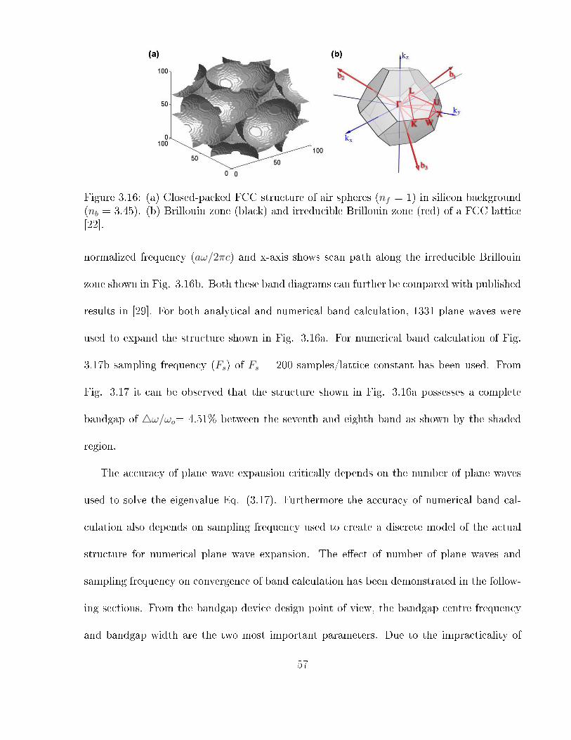
Figure 3.16: (a) Closed-packed FCC structure of air spheres (nf = 1) in silicon background(nb = 3.45). (b) Brillouin zone (black) and irreducible Brillouin zone (red) of a FCC lattice[22].
normalized frequency (aω/2πc) and x-axis shows scan path along the irreducible Brillouin
zone shown in Fig. 3.16b. Both these band diagrams can further be compared with published
results in [29]. For both analytical and numerical band calculation, 1331 plane waves were
used to expand the structure shown in Fig. 3.16a. For numerical band calculation of Fig.
3.17b sampling frequency (Fs) of Fs = 200 samples/lattice constant has been used. From
Fig. 3.17 it can be observed that the structure shown in Fig. 3.16a possesses a complete
bandgap of 4ω/ωo= 4.51% between the seventh and eighth band as shown by the shaded
region.
The accuracy of plane wave expansion critically depends on the number of plane waves
used to solve the eigenvalue Eq. (3.17). Furthermore the accuracy of numerical band cal-
culation also depends on sampling frequency used to create a discrete model of the actual
structure for numerical plane wave expansion. The e�ect of number of plane waves and
sampling frequency on convergence of band calculation has been demonstrated in the follow-
ing sections. From the bandgap device design point of view, the bandgap centre frequency
and bandgap width are the two most important parameters. Due to the impracticality of
57
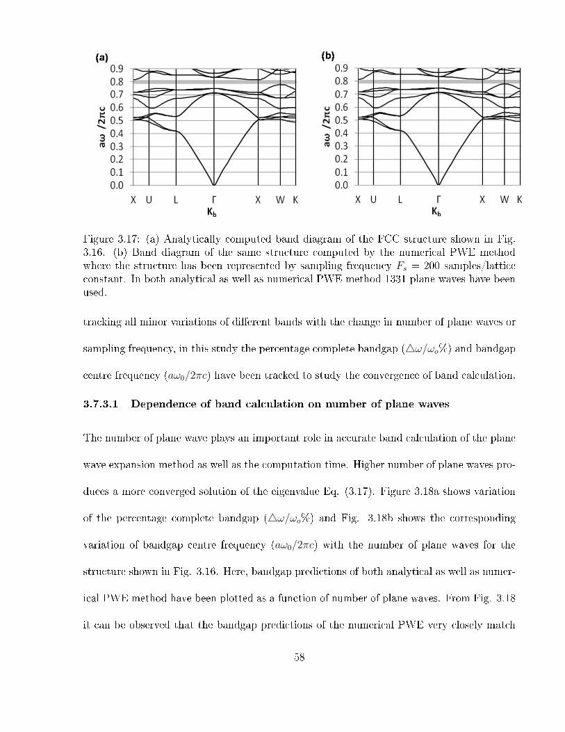
Figure 3.17: (a) Analytically computed band diagram of the FCC structure shown in Fig.3.16. (b) Band diagram of the same structure computed by the numerical PWE methodwhere the structure has been represented by sampling frequency Fs = 200 samples/latticeconstant. In both analytical as well as numerical PWE method 1331 plane waves have beenused.
tracking all minor variations of di�erent bands with the change in number of plane waves or
sampling frequency, in this study the percentage complete bandgap (4ω/ωo%) and bandgap
centre frequency (aω0/2πc) have been tracked to study the convergence of band calculation.
3.7.3.1 Dependence of band calculation on number of plane waves
The number of plane wave plays an important role in accurate band calculation of the plane
wave expansion method as well as the computation time. Higher number of plane waves pro-
duces a more converged solution of the eigenvalue Eq. (3.17). Figure 3.18a shows variation
of the percentage complete bandgap (4ω/ωo%) and Fig. 3.18b shows the corresponding
variation of bandgap centre frequency (aω0/2πc) with the number of plane waves for the
structure shown in Fig. 3.16. Here, bandgap predictions of both analytical as well as numer-
ical PWE method have been plotted as a function of number of plane waves. From Fig. 3.18
it can be observed that the bandgap predictions of the numerical PWE very closely match
58
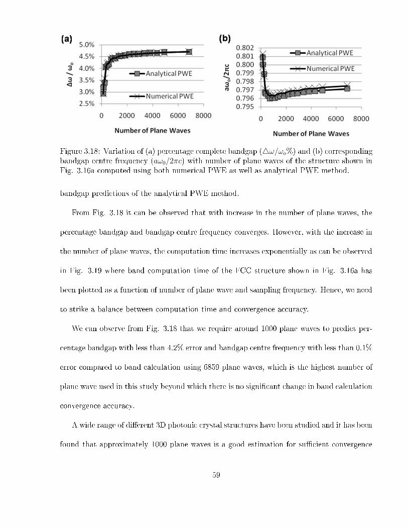
Figure 3.18: Variation of (a) percentage complete bandgap (4ω/ωo%) and (b) correspondingbandgap centre frequency (aω0/2πc) with number of plane waves of the structure shown inFig. 3.16a computed using both numerical PWE as well as analytical PWE method.
bandgap predictions of the analytical PWE method.
From Fig. 3.18 it can be observed that with increase in the number of plane waves, the
percentage bandgap and bandgap centre frequency converges. However, with the increase in
the number of plane waves, the computation time increases exponentially as can be observed
in Fig. 3.19 where band computation time of the FCC structure shown in Fig. 3.16a has
been plotted as a function of number of plane wave and sampling frequency. Hence, we need
to strike a balance between computation time and convergence accuracy.
We can observe from Fig. 3.18 that we require around 1000 plane waves to predict per-
centage bandgap with less than 4.2% error and bandgap centre frequency with less than 0.1%
error compared to band calculation using 6859 plane waves, which is the highest number of
plane wave used in this study beyond which there is no signi�cant change in band calculation
convergence accuracy.
A wide range of di�erent 3D photonic crystal structures have been studied and it has been
found that approximately 1000 plane waves is a good estimation for su�cient convergence
59

Figure 3.19: Band computation time of the FCC structure shown in Fig. 3.16a has beenplotted as a function of number of plane wave and sampling frequency.
accuracy of the band calculation.
3.7.3.2 Dependence of band calculation on sampling frequency
The accuracy of any numerical technique depends on discretization process of replicating the
original structure into a discrete numerical model. To avoid aliasing e�ects, higher sampling
frequency is always preferred for accurate representation of higher spatial frequency compo-
nents of the real structure. However, higher sampling frequency requires higher computation
memory. Hence, there needs to be a balance between structural accuracy and sampling fre-
quency. Figure 3.20 shows the e�ect of sampling frequency on band calculation of the same
closed packed FCC structure of air spheres in a silicon background as shown in Fig. 3.16a.
To highlight the importance of sampling frequency, bandgap predictions of numerical
PWE have been compared with the analytical PWE method, which does not depend on
sampling frequency. As predicted by the analytical PWE method, this structure possesses
60

Figure 3.20: Variation of (a) percentage bandgap and (b) corresponding bandgap centrefrequency with sampling frequency of the structure shown in Fig. 3.16a.
a complete bandgap of 4.50% computed with 1331 plane waves. Corresponding numerical
band calculation has been performed for a large range of sampling frequency of Fs = 25-200
samples/lattice constant using 1331 plane waves and the corresponding bandgap predictions
have been compared with analytical PWE predictions. It can be observed in Fig. 3.20
that with the increase in sampling frequency, the numerical band calculation prediction of
percentage bandgap and bandgap centre frequency converges to the corresponding analytical
predictions. Hence, it can be concluded that to avoid aliasing related inaccuracies in the
numerical bandgap calculation of a given structure, the sampling frequency should be above
a threshold value. However, this threshold value depends on the spatial frequency contents
of a given structure and hence will vary from structure to structure.
3.8 Summary
In this chapter, the theoretical foundation of the present research work has been laid out.
The under-laying physics behind di�ractive optics lithography has been discussed in terms of
61
Talbot self-imaging phenomenon. Lattice constants have been de�ned for the crystal lattice
formed with a 3D periodic arrangement of Talbot self-images. The beam walk-o� has been
characterized to de�ne a practical working depth of near-�eld. E�ects of relative di�raction
e�ciency and polarization on near-�eld intensity distribution have been examined. The
theory behind photonic band calculation has been discussed. Details of numerical band
calculation have been elaborated with an example band calculation.
62
Chapter 4
Di�ractive optics for fabrication of
diamond-like structures
4.1 Introduction
A wide range of 3D photonic crystal structures have been proposed and fabricated over
the past two decades [11]. Both diamond and diamond-like structures characterized by
double basis on a face-centered-cubic (FCC) or tetragonal (TTR) point Bravais lattice are
very attractive for their wide complete bandgap when fabricated with high refractive index
materials [24]. However, fabrication of diamond or diamond-like structures is challenging
and tedious due to the double basis nature of their crystal geometry. In our di�ractive
optics lithography research, three DOE design have been proposed to fabricate diamond-like
woodpile structure. In our initial work we have used 1D-DOE for two independent orthogonal
laser exposures to fabricate diamond-like structure by interlacing two 2D periodic structures.
To improve fabrication accuracy subsequently we present two single exposure methods based
on phase-tunable and multi-level DOEs.
63
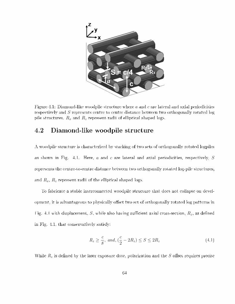
Figure 4.1: Diamond-like woodpile structure where a and c are lateral and axial periodicitiesrespectively and S represents centre to centre distance between two orthogonally rotated logpile structures. Rx and Rz represent radii of elliptical shaped logs.
4.2 Diamond-like woodpile structure
A woodpile structure is characterized by stacking of two sets of orthogonally rotated logpiles
as shown in Fig. 4.1. Here, a and c are lateral and axial periodicities, respectively, S
represents the centre-to-centre distance between two orthogonally rotated log-pile structures,
and Rx, Rz represent radii of the elliptical shaped logs.
To fabricate a stable interconnected woodpile structure that does not collapse on devel-
opment, it is advantageous to physically o�set two set of orthogonally rotated log patterns in
Fig. 4.1 with displacement, S, while also having su�cient axial cross-section, Rz, as de�ned
in Fig. 4.1, that conservatively satisfy:
Rz ≥c
8, and , (
c
2− 2Rz) ≤ S ≤ 2Rz (4.1)
While Rz is de�ned by the laser exposure dose, polarization and the S o�set requires precise
64

shift between the two set of log patterns. According to Eq. (4.1), Rz = c/8 de�nes the lowest
exposure threshold at which Eq. (4.1) demands an exact quarter period o�set of S = c/4,
while any o�set value is acceptable for Rz > c/4.
4.3 Bandgap optimization of woodpile structure
From the ongoing development, it is evident that with suitable selection of optical materials
and DOE design, a stable interconnected 3D woodpile structure can be fabricated following
any of the three di�ractive optics lithography methods explored here. While such woodpile
structures can be classi�ed as face centered cubic (FCC) or tetragonal (TTR) lattice symme-
try [52], the TTR irreducible Brillouin zone is known to be a more appropriate symmetry [52]
for woodpile structures. Hence, we base our band dispersion calculations on TTR symmetry.
To predict the band positions, band dispersion curves were calculated using the numerical
plane wave expansion (PWE) method as described in Section 3.7.2.
4.3.1 Complete bandgap
Calculations were carried out over a wide range of c/a ratios (1 < c/a < 3) and laser exposure
levels (�lling fractions of 10% <f < 90%) to identify the experimental exposure parameters
that provide the widest bandgap for laser-formed templates inverted with silicon. The �lling
fraction could be controlled by varying any combination of laser intensity, polarization and
exposure time as discussed in Section 3.6. Unlike the c/a ratio, the �lling fraction has no
closed form expression to produce a desired structure and required an iterative method of
optimization. The c/a range was restricted by the λd/Λ ratio as de�ned in Eq. (4.2) by our
choice of nr = 1.6 for the refractive index of SU-8 photoresist, ni = 1.9 for an incidence index
65

matching medium, and nd = 1.9 for a high index DOE substrate. The relative intensity of
di�raction orders is controllable by the DOE etch depth as discussed in Section 3.5.1 and
values of 30%, 30% and 30% were assumed for the -1st , 0th and 1st orders, respectively.
The laser polarization was linear in both exposure orientations. The 3D intensity pattern
was calculated for two equal intensity DOE exposures as described in Section 4.4.1 and
then set to a threshold intensity that �nally yielded an isointensity surface de�ning the 3D
structure of the photoresist. This numerical calculation yielded an irregularly shaped motif,
from which numerical band calculations [49] provided energy dispersion curves. A direct
band calculation of the polymer structure with c/a = 1.2 and f ≈ 25% is shown in Fig.
4.2a. Values of S = c/4 and Rz = c/8 were selected to satisfy the interlacing condition (Eq.
(4.1)) for a woodpile structure. This polymer structure provided an 8.1% bandgap along
the Γ-Z direction�indicated by the hatching�but does not provide a complete photonic
bandgap due to a low refractive index contrast of nr - nair = 0.6 for the photoresist template
. However, if we double invert this structure using known procedures [16] to create a silicon
log structure with an air background, a similar calculation yields the band dispersion curves
of Fig. 4.2b where a complete bandgap of 4ω/ω0 = 18.5% is identi�ed by the hatched area.
4.3.2 Optimized DOE parameters
The spectral width of the bandgap strongly depends on the c/a ratio, which, in turn, is easily
controlled (Eq. 3.4) by the ratio of laser wavelength to DOE periodicity (λd/Λ). Figure 4.3
shows the dependence of complete bandgap width (4ω/ω0 ) for the double-inverted silicon
structures with λd/Λ ratio for a constant �lling fraction of f ≈ 25%. The top axis shows
the corresponding variation with c/a ratio. The maximum bandgap is noted at λd/Λ =
66

Figure 4.2: Band dispersion diagram (a) for 3D woodpile structure in photoresist for valuesof n =1.6, c/a = 1.2, and f ≈ 25% and (b) modi�ed dispersion diagram with the samestructure after double inversion to a silicon woodpile with n = 3.45, c/a = 1.2, and f ≈ 25%.
0.98nr≈1.57 just before the cut o� for total internal re�ection at λd/Λ = 1.6. The energy
dispersion curve in Fig. 4.2b is plotted for this maximum bandgap condition.
Flexibility of achieving a desired axial-to-transverse periodicity ratios, c/a, is crucial in
fabricating photonic crystals because a complete photonic bandgap in such structures is
available only in a narrow range of, c/a ratio. DOEs provide wide latitude here for varying
the c/a ratio and thereby optimizing the bandgap properties. However, the maximum allowed
value of the normalized wavelength (λd/Λ) is dictated by total internal re�ection condition
at various interfaces as given in Eq. (4.2). According to Eq. (3.4), c/a depends principally on
the DOE period (Λ), refractive index of the photoresist (nr) and laser wavelength (λd) and
is plotted in Fig. 4.4 as a function of the normalized wavelength, λd/Λ, for SU-8 photoresist
(nr = 1.6) following laser exposure arrangement of Fig. 3.2.
According to Fig. 4.4, the near-symmetric periodic structure can be achieved with a
small period DOE such that Λ ∼ λd. However, this condition yields high di�raction angles
67
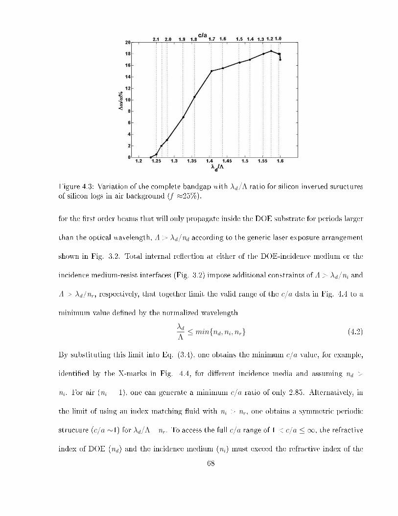
Figure 4.3: Variation of the complete bandgap with λd/Λ ratio for silicon inverted structuresof silicon logs in air background (f ≈25%).
for the �rst order beams that will only propagate inside the DOE substrate for periods larger
than the optical wavelength, Λ > λd/nd according to the generic laser exposure arrangement
shown in Fig. 3.2. Total internal re�ection at either of the DOE-incidence medium or the
incidence medium-resist interfaces (Fig. 3.2) impose additional constraints of Λ > λd/ni and
Λ > λd/nr , respectively, that together limit the valid range of the c/a data in Fig. 4.4 to a
minimum value de�ned by the normalized wavelength
λdΛ≤ min{nd, ni, nr} (4.2)
By substituting this limit into Eq. (3.4), one obtains the minimum c/a value, for example,
identi�ed by the X-marks in Fig. 4.4, for di�erent incidence media and assuming nd >
ni . For air (ni = 1), one can generate a minimum c/a ratio of only 2.85. Alternatively, in
the limit of using an index matching �uid with ni > nr , one obtains a symmetric periodic
structure (c/a ∼1) for λd/Λ= nr . To access the full c/a range of 1 < c/a ≤ ∞, the refractive
index of DOE (nd) and the incidence medium (ni) must exceed the refractive index of the
68

Figure 4.4: Variation of c/a ratio in SU-8 photoresist (nr = 1.6) with normalized wavelengthλd/Λ for di�erent refractive index values of the incidence medium (ni).
photoresist according to Eq. (4.3).
{nd , ni} ≥ nr ; 1 <c
a≤ ∞ (4.3)
Larger ni and nr values are attractive to reduce Fresnel losses, but exact c/a = 1 ratio is not
achievable in this near-�eld di�ractive optics method for any value of nd , ni and nr because
the condition λd/Λ = nr required to achieve c/a = 1 implies a di�raction angle of θ1 = 90o
with no e�ective beam overlap region.
4.4 Di�ractive optics for diamond-like structure
Due to the double basis, special DOE designs are required in order to create diamond-like
near-�eld di�raction pattern. As mentioned in Section 3.3.1 a two-dimensional DOE is re-
quired for creating a 3D intensity distribution. However, a binary 2D DOE creates a 3D
di�raction pattern of single basis structure arranged on body-centered-tetragonal (BCT)
point Bravais lattice as shown in Fig. 3.2b. Hence, to circumvent this problem, in our
69

initial work we have used 1D-DOE for two independent orthogonal laser exposures to fab-
ricate diamond-like structure by interlacing of two 2D structures. The required shift S =
c/4 between two orthogonally rotated di�raction pattern is provided by precise physical dis-
placement between DOE and sample between two laser exposures. To improve fabrication
accuracy, we subsequently proposed two single laser exposure methods based on a phase-
tunable DOE and a multi-level 2D-DOE. In the phase-tunable DOE method the shift S is
controlled by tuning the phase di�erence of one set of �rst order di�racted beams whereas in
multi-level DOE method a �xed di�erence between the two phase levels was used to control
the shift S.
4.4.1 One-dimensional DOE based double laser exposure method
Our group was �rst to extend DOEs to the fabrication of 3D photonic crystal templates,
creating diamond-like woodpile structures in SU-8 photoresist by two sequential exposures
of orthogonal one-dimensional DOEs (1D-DOE) with an Ar-ion laser [15, 43, 53]. In this
section a general theoretical guideline for fabricating woodpile photonic crystal templates by
the double-exposure 1D-DOE method is presented.
4.4.1.1 One-dimensional phasemask design
For demonstration purposes, two commercially available �ber Bragg grating writing fused
silica (nd = 1.46) phasemasks having period Λ = 1.066 µm and groove depth dt = 265 nm have
been used in fabricating woodpile structure using this double laser exposure method. The
RCWA based di�raction e�ciency calculation of the phasemask is shown in Fig. 4.5 for laser
light of wavelength λd = 488 nm having polarization vector parallel to the grating grooves
(TM polarized). According to the di�raction e�ciency calculation the groove depth dt = 265
70
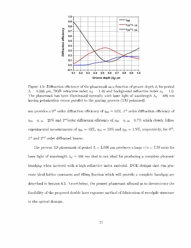
Figure 4.5: Di�raction e�ciency of the phasemask as a function of groove depth dt for periodΛ = 1.066 µm, DOE refractive index nd = 1.46 and background refractive index nb = 1.0.The phasemask has been illuminated normally with laser light of wavelength λd = 488 nmhaving polarization vector parallel to the grating grooves (TM polarized).
nm provides a 0th order di�raction e�ciency of η00 = 55%, 1st order di�raction e�ciency of
η10= η−10= 20% and 2ndorder di�raction e�ciency of η20= η−20= 0.7% which closely follow
experimental measurements of η00 = 53%, η10 = 19% and η20 = 1.5%, respectively, for 0th,
1st and 2nd order di�racted beams.
The present 1D phasemask of period Λ = 1.066 µm produces a large c/a = 7.29 ratio for
laser light of wavelength λd = 488 nm that is not ideal for producing a complete photonic
bandgap when inverted with a high refractive index material. DOE designs that can gen-
erate ideal lattice constants and �lling fraction which will provide a complete bandgap are
described in Section 4.3. Nevertheless, the present phasemask allowed us to demonstrate the
feasibility of the proposed double laser exposure method of fabrication of woodpile structure
in the optical domain.
71

Figure 4.6: Formation of multiple di�racted beams from a single laser beam by a 1D-DOEand arrangement for photoresist exposure.
4.4.1.2 Interlacing of two orthogonally rotated interference patterns
Figure 4.6 shows the separation of an incident laser beam into m = +1st, 0th, and −1st
di�raction orders after passing through a 1D-DOE of period, Λ= 1.066 µm. In the overlap
volume immediately below the DOE, the di�racted beams create a near-�eld 2D log-pile
type interference pattern as shown in Fig. 4.7a. The 2D periodic interference pattern
can be accurately captured with a thick (� c) negative photoresist placed in the beam
overlap region of Fig. 4.6 and by applying a laser exposure that just exceeds the photo-
polymerization threshold of the photoresist. Post exposure development then solidi�es the
polymerized volume and dissolves the under-exposed volume to replicate the interference
pattern.
To create a 3D periodic structure, the �rst 1D-DOE exposure (Fig. 4.7a) is followed by
a second exposure with an identical but orthogonally rotated 1D-DOE, creating the rotated
72

Figure 4.7: Periodic near-�eld di�raction patterns created by (a) a single exposure with a1D-DOE, (b) a single exposure with a similar 1D-DOE rotated by 90o, and (c) the resultinginterlaced 3D woodpile structure due to combination of the two exposures in (a) and (b)with shift S = c/4 between two exposures.
2D log-pile intensity pattern show in Fig. 4.7b. The combination of these two sequential
exposures then yields an intensity pattern approximately described by the interlaced 3D
woodpile structure as shown in Fig. 4.7c. To form a double basis with the two orthogonally
rotated interlaced structures, a precise motion controlled stage was used along the optical
axis to accurately displace one of the DOE masks by S = c/4 between two laser exposures.
Although, the �gure cartoons in Fig. 4.7 depict uniform elliptical-like cross-sections with
asymmetric radii, Rx and Rz, the sum of two interference patterns are more complex than
shown. A more precise representation of the intensity distribution can be easily generated
by the methods in Section 3.5.2.2 with numerical computations that account for laser polar-
ization together with the di�raction e�ciencies and angles that depend on the groove depth
and DOE period. The �nal structure of the photoresist is further governed by complex re-
lations between laser exposure dose, photoresist exposure threshold, shrinkage and chemical
di�usion. Such more accurate isointensity distributions will be presented and compared with
observations of the fabricated structures in Chapter 6.
73

4.4.2 Phase tunable DOE for single exposure method
As discussed in the previous section, a diamond-like woodpile photonic crystal structure is
to be formed with di�ractive optics lithography by two sequential laser exposures of photore-
sist using two orthogonally rotated 1D binary phasemasks. However, imprecise alignment
between two DOE exposures prevents this method from reproducibly interlace two 2D struc-
tures and a single exposure DOE method is therefore preferred for improved uniformity
and reproducibility of the 3D structures. In this section, we present a phase-tunable DOE
that has enabled formation of a 3D photonic crystal template with a single laser exposure.
The phase-tunable DOE was constructed by orthogonal combination of two linear phase-
masks. Controlled separation of the two optical elements provided a variable phase shift
to manipulate the interlacing position of two orthogonally rotated periodic structures, and
thereby facilitate fabrication of diamond-like woodpile structures having tetragonal (TTR)
symmetry through to structures we predict to have body-centered-tetragonal (BCT) symme-
try, and including variations in between. Finite di�erence time domain (FDTD) calculation
of interference patterns and associated isointensity surfaces are corroborated by de�nitive
demonstrations of TTR and BCT symmetry structures inside photoresist that smoothly
transform from TTR to BCT symmetry by the DOE phase shift.
4.4.2.1 Phase tunable DOE
The proposed phase tunable DOE design for single-exposure 3D patterning centers on or-
thogonal alignment of two similar linear phasemasks, positioned back-to-back as shown Fig.
4.8. The DOE is illuminated at normal incidence by a laser beam of wavelength λd as shown
in Fig. 4.8. A pressure adjustable mount varies the separation, d, between the two phase-
74

Figure 4.8: Phasemask arrangement de�ning a two-dimensional DOE and providing ad-justable separation, d, for phase shift control of near-�eld di�raction patterns.
masks to control the phase shift, 4φ, between two 2D interference patterns generated in the
z-x and z-y planes below the DOE. This gap or phase shift is pivotal in controlling the TTR-
to-BCT symmetry by manipulating the near-�eld interference patterns formed inside the
photoresist (nr) positioned directly below the multi-level DOE. These patterns are modeled
by di�raction theory [40,54] given in Section 3.5.2.2.
4.4.2.2 Phase control principles
The top phasemask in Fig. 4.8 generates three strong di�racted beams of h1(0, 0) in zeroth
order and h1(1, 0) and h1(−1, 0) in �rst orders, provided λd /Λ < ngap is satis�ed. Here, ngap
is the refractive index of the gap and the refractive index of both phasemasks is nd. Due to
di�erent propagation paths, the 0th-order and 1st-order di�racted beams accumulate a phase
di�erence prior to arrival at the second grating surface, given by:
4φ =∑i
ki
10.li
10 −∑i
ki
00.li
00 (4.4)
where ki
10 , ki
00 are wave vectors corresponding to h1(1, 0) , h1(0, 0) di�racted beams respec-
tively and li
10 , li
00, are corresponding path vectors inside the i-th medium of the 2D-DOE.
75

For wave propagation through two phasemask substrates (nd) of thickness d1 and the gap
(ngap) between them of thickness d and considering snell's law at each interface, the phase
di�erence (∆φ) becomes:
4φ =2π
λ[ngapd
f(ngap)+
2ndd1
f(nd)] (4.5)
where
f(nv) =
√[1− (λd/nvΛ)2]
1−√
[1− (λd/nvΛ)2], for nv = ngap, nd
These three beams are further di�racted by the second grating interface, creating the
following �ve principle di�racted beams:
h1(0, 0)⇒ {h2(0, 1), h2(0, 0), h2(0,−1)}
h1(1, 0)ej4φ ⇒ {h2(1, 0)}ej4φ (4.6)
h1(−1, 0)ej4φ ⇒ {h2(−1, 0)}ej4φ
It is evident from Eq. (4.6) that 2D log-pile patterns are separately generated in each of
the z-y and z-x planes by interference amongst the h2(0, 1), h2(0,−1) with h2(0, 0) di�racted
beams in the former and the h2(1, 0), h2(−1, 0)ej4φ with h2(0, 0) di�racted beams in the
latter. A 3D periodic structure then results from the interlacing of these two 2D log pile
structures inside the photoresist. Here, a small variation of phasemask gap, d, in Eq. (4.5) is
seen in Eq. (4.6) to introduce a controllable phase shift, 4φ, between these two orthogonal
log patterns. In this way, one can spatially control this interlacing o�set to manipulate the
symmetry of the 3D periodic structure formed inside the photoresist of Fig. 4.8. The phase
shift then yields a spatial o�set, S, of the x- and y-oriented logs in the axial direction, which
can be folded by the periodicity of the lattice into the reduced range 0 ≤ S ≤ c/4 and de�ned
by:
76

Figure 4.9: The 3D structure representations of DOE near-�eld di�raction patterns generatedby interlacing of two 2D log structures: (a) BCT symmetry structure for S = 0, and (b)diamond-like woodpile structure with TTR symmetry for S = c/4.
S =c
2π4φ where S(0) = S(m
c
2), ∀m ∈ Z (4.7)
This range encompasses all available crystal symmetries that span from BCT at S = 0
to TTR at S = c/4. Figure 4.9a depicts the interlacing of x- and y-oriented logs on the
same horizontal planes for the condition of S = 0 (or c/2) and these inter-penetrated logs
get arranged with a single basis on a body centered tetragonal (BCT) lattice. The other
extreme case of S = c/4 separates these to orthogonally rotated structures axially and hence
logs get arranged with a double basis on a tetragonal (TTR) lattice de�ning a diamond-like
woodpile structure as shown in Fig. 4.9b.
The structural symmetry cycles periodically between TTR (for m = 1, 2, 3. . . ) and BCT
(m = 2, 4, 6. . . ) lattices as the phasemask gap, d, increases according to:
d = [m
4
λ
ngap− 2ndd1
ngapf(nd)]f(ngap) (4.8)
77

4.4.2.3 Finite di�erence time domain predictions of phase tunable near-�eld
di�raction pattern
To fabricate a woodpile structure with a phase-tunable DOE which will demonstrate com-
plete bandgap after inversion requires an optimized DOE design as given in Section 4.3. A
high refractive index material between the two phasemasks of ngap> nr is also required [55].
However, for experimental demonstration two commercially fabricated phasemasks having
the same period Λ = 1.066 µm as used in the double exposure method of Section 4.4.1 were
used here as back-to-back connected masks with air gap (ngap= 1) between them. To better
predict the 3D structures generated by the DOE device in Fig. 4.8, �nite di�erence time
domain (FDTD) computation was used to generate time averaged intensity distributions,
<I(x,y)>, in the photoresist layer (SU-8, nr = 1.6) for various air gaps (ngap= 1), d, between
two phasemasks. Plane wave TE polarized light of λd = 514 nm was propagated through the
phase-tunable DOE where TE polarization is de�ned as polarization vector perpendicular
to the grating grooves. Figure 4.10 shows 2D intensity distributions (<I(x,y)>) calculated
for a �xed z = zo plane that intercepts the center of x-oriented logs. The image sequence
runs a full cycle of S o�set values that progresses from a TTR structure de�ned by S = c/4
for the gap d = 0.9084 µm (Fig. 4.10a), to a BCT structure at S = c/2 (or 0) for the gap
d = 1.816 µm (Fig. 4.10b), to a TTR structure at S = 3c/4 (or c/4) for the gap d =2.725
µm (Fig. 4.10c), and returning to a BCT structure at S = c (or 0) for the gap d = 3.634
µm (Fig. 4.10d). As predicted, the intersection points of orthogonally overlapping logs for
S = 0 (Fig. 4.10b) and S = c (or 0) (Fig. 4.10d) are identical and manifest in near-circular
intensity pro�les that are arranged on a periodic square grid corresponding to the top surface
of the BCT lattice as shown in Fig. 4.9a. Patterns for S = c/4 (Fig. 4.10a) and S = 3c/4
78
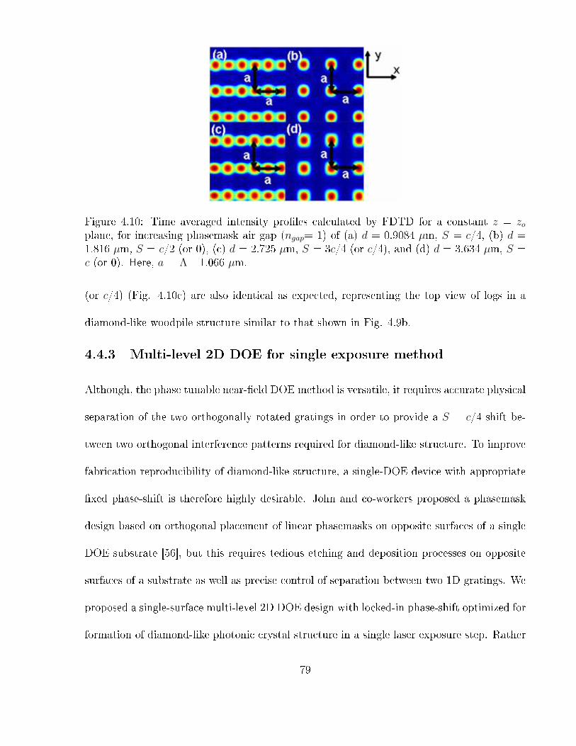
Figure 4.10: Time averaged intensity pro�les calculated by FDTD for a constant z = zoplane, for increasing phasemask air gap (ngap= 1) of (a) d = 0.9084 µm, S = c/4, (b) d =1.816 µm, S = c/2 (or 0), (c) d = 2.725 µm, S = 3c/4 (or c/4), and (d) d = 3.634 µm, S =c (or 0). Here, a = Λ= 1.066 µm.
(or c/4) (Fig. 4.10c) are also identical as expected, representing the top view of logs in a
diamond-like woodpile structure similar to that shown in Fig. 4.9b.
4.4.3 Multi-level 2D DOE for single exposure method
Although, the phase tunable near-�eld DOE method is versatile, it requires accurate physical
separation of the two orthogonally rotated gratings in order to provide a S = c/4 shift be-
tween two orthogonal interference patterns required for diamond-like structure. To improve
fabrication reproducibility of diamond-like structure, a single-DOE device with appropriate
�xed phase-shift is therefore highly desirable. John and co-workers proposed a phasemask
design based on orthogonal placement of linear phasemasks on opposite surfaces of a single
DOE substrate [56], but this requires tedious etching and deposition processes on opposite
surfaces of a substrate as well as precise control of separation between two 1D gratings. We
proposed a single-surface multi-level 2D DOE design with locked-in phase-shift optimized for
formation of diamond-like photonic crystal structure in a single laser exposure step. Rather
79

than rely on the precise control of substrate thickness [56], or the accurate physical sepa-
ration of two DOEs for phase control [35], a phase shift was built into the single-surface
DOE design which further enables ease of etching of di�ractive elements on a single side of
a substrate.
4.4.3.1 Two-level vs. proposed three-level 2D DOE
A two-level 2-dimensional DOE is characterized by two phase levels (binary) and two lattice
constants. Figure 4.11a shows a two-level square lattice 2D DOE having groove depth of d
and equal periodicities of Λx = Λy = Λ. The DOE has groove refractive index nd which is
immersed in background refractive index nb to de�ne two phase levels of optical thicknesses
ndd and nbd as shown in Fig. 4.11a. One typical laser exposure arrangement showing index
matching medium (ni) between the DOE substrate (ns) and the photoresist (nr) layer which
is spun onto a substrate of refractive index ns has been shown in Fig. 4.11b. However,
as described in Chapter 3, the Talbot self-images of a two dimensional DOE having two
phase levels repeats along the optical axis forming a 3D di�raction pattern of single basis
structure arranged on a body-centered-tetragonal (BCT) point Bravais lattice. This lead to
the conclusion that more complex phase pro�le is required in order to fabricate double basis
structures.
To form a double basis diamond-like structure, we propose a three-level DOE. Figure
4.12a shows the proposed three-level DOE having a speci�c phase pro�le so that in the near-
�eld phase-fronts of interfering di�racted beams interfere to create a diamond-like intensity
distribution. The DOE is characterized by equal periodicities Λx = Λy= Λ and asymmetrical
depths d1 and d2 of the orthogonal grooves. The DOE-patterned �lm has refractive index
80

Figure 4.11: (a) A two-level 2D DOE having groove depth of d and equal periodicities of Λx
= Λy=Λ. (b) One typical laser laser exposure arrangement showing index matching medium(ni) between DOE substrate (ns) and photoresist (nr) layer which is spun onto a substrateof refractive index ns.
Figure 4.12: A three-level DOE (a) color-coded for each phase level as de�ned by orthogonalgrooves of periodicities Λx and Λy, depths d1 and d2 and refractive indices nd1 and nd2 ina background medium of refractive index nb; and (b) laser exposure arrangement showingindex matching medium (ni) between DOE substrate (ns) and photoresist (nr) layer whichis spun onto a substrate of refractive index ns.
nd1 (blue) and nd2 (green) which is immersed in background refractive index nb to de�ne
four di�erent phase levels. For nd = nd1 = nd2 , this reduces to three phase levels of optical
thicknesses ndd2, ndd1+ nb(d2-d1), and nbd2 in Fig. 4.12a.
4.4.3.2 Working principles of three-level DOE
The groove depths, d1 and d2 of the proposed multi-level DOE are important in controlling
the e�ciency of various di�raction orders, which, in turn, de�ne the motif and possibilities
for linking a stable lattice together at an appropriate �lling fraction. In the simple case of a
81
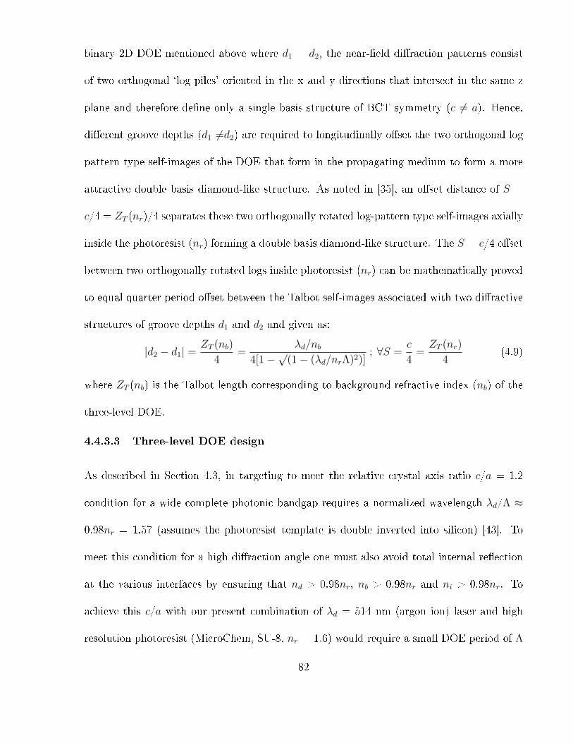
binary 2D DOE mentioned above where d1 = d2, the near-�eld di�raction patterns consist
of two orthogonal `log piles' oriented in the x and y directions that intersect in the same z
plane and therefore de�ne only a single basis structure of BCT symmetry (c 6= a). Hence,
di�erent groove depths (d1 6=d2) are required to longitudinally o�set the two orthogonal log
pattern type self-images of the DOE that form in the propagating medium to form a more
attractive double basis diamond-like structure. As noted in [35], an o�set distance of S =
c/4 = ZT (nr)/4 separates these two orthogonally rotated log-pattern type self-images axially
inside the photoresist (nr) forming a double basis diamond-like structure. The S = c/4 o�set
between two orthogonally rotated logs inside photoresist (nr) can be mathematically proved
to equal quarter period o�set between the Talbot self-images associated with two di�ractive
structures of groove depths d1 and d2 and given as:
|d2 − d1| =ZT (nb)
4=
λd/nb4[1−
√(1− (λd/nrΛ)2)]
; ∀S =c
4=ZT (nr)
4(4.9)
where ZT (nb) is the Talbot length corresponding to background refractive index (nb) of the
three-level DOE.
4.4.3.3 Three-level DOE design
As described in Section 4.3, in targeting to meet the relative crystal axis ratio c/a = 1.2
condition for a wide complete photonic bandgap requires a normalized wavelength λd/Λ ≈
0.98nr = 1.57 (assumes the photoresist template is double inverted into silicon) [43]. To
meet this condition for a high di�raction angle one must also avoid total internal re�ection
at the various interfaces by ensuring that nd > 0.98nr, nb > 0.98nr and ni > 0.98nr. To
achieve this c/a with our present combination of λd = 514 nm (argon ion) laser and high
resolution photoresist (MicroChem, SU-8, nr = 1.6) would require a small DOE period of Λ
82
= 327 nm which is beyond our present multi-level DOE fabrication capabilities of period Λ
∼ 650 nm. A longer source wavelength of λd ≈ 1020 nm was not a desirable alternative due
to the poor response of photoresist at this wavelength and lower overall expected resolution.
A compromise of a larger c/a ratio was necessary. Commercial DOEs are now available as
a binary 2D phasemask with periods typically around 1 µm. Multi-level masks with high
resolution features on the scale of∼250 nm required here are very challenging to fabricate and
must be custom fabricated. The proposed three-level DOE was directly written on thin (1 to
2 µm) photoresist (SU-8 2002, nd = 1.6) by two-photon polymerization with a femtosecond
laser. After testing the resolution, uniformity, and reproducibility of this method over a large
writing (5 mm x 5 mm) area, a period of Λ= 650 nm was selected as the minimum practical
value for testing the proposed 3-level DOE design. However, according to Eq. (3.4), this
combination predicts a large c/a ratio of 3.78 than the c/a = 1.2 value required for a wide
complete photonic bandgap. Further e�ort to develop shorter period DOEs together with
the use of higher refractive index media and longer wavelength laser light would lead to the
more desirable c/a = 1.2 ratio. Nevertheless, the proposed c/a = 3.78 ratio is a signi�cant
improvement over our previous demonstration of c/a = 6.91 which was based on much
larger grating period of Λ = 1.066 µm [35, 43, 55]. The merits of multi-level DOE can thus
be tested in this new high resolution regime for 3D photonic crystal fabrication. With the
DOE design set to Λ = 650 nm period and λd = 514 nm laser wavelength, groove depths,
d2 and d1, were optimized to balance and ideally distribute the intensities of the various
DOE di�raction orders to produce an uniform diamond-like 3D intensity distribution in the
photoresist. Isointensity surfaces were calculated and followed with bandgap calculations
as described below to optimize the bandgap properties of the expected template both in
83

Figure 4.13: Di�raction e�ciency of a three-level DOE (Fig. 4.12a) as a function of groovedepth d1 with a �xed groove di�erence (d2 - d1) = 331 nm for diamond-like structure. Inset(i) shows the unit cell with d2 and d1 phase elements of refractive index, nd = 1.6, in airbackground (nb = 1.0) and substrate refractive index ns =1.46.
photoresist and after double inversion in silicon.
A �xed value of (d2 � d1) = 331 nm was obtained from Eq. (4.9) for the S = c/4 o�set
required for a diamond-like woodpile structure. To avoid high aspect ratio DOE grooves
that might be di�cult to laser-fabricate in the SU-8 photoresist (nd = 1.6), an air (nb =
1.0) background was selected for maximum index contrast. Figure 4.13 shows di�raction
e�ciencies calculated as a function of DOE groove depth d1 by rigorous couple wave analysis
(RCWA) based commercial algorithm (GSolver Ltd.). Circularly polarized plane wave light
was used to avoid the strong polarization e�ects that otherwise imbalance (i.e. η10 6= η01)
the x- and y-direction 1st order DOE di�raction e�ciencies [55]. The color coded unit cell
of the phase pro�le used in the di�raction e�ciency estimation is shown in the inset-(i) of
Fig. 4.13. The area of phase element d2 occupies 50% of total area of the unit cell and d1
and background (nb) phase elements occupy 25% of total area each. For this combinations
of laser wavelength (λd = 514 nm), DOE period (Λ = 650 nm) and substrate refractive index
84

(ns =1.46), there is no higher order di�racted beams (|m|, |n| ≥2) as well as due to very low
di�raction e�ciencies of < 1%, the 1st order cross beams (|m|=|n| =1) has been ignored.
To ensure uniform 3D intensity distribution and better local laser exposure dose control,
according to Fig. 4.13 DOE groove depths d1 = 1.13 µm, thus yielding d2 = d1 + 0.331 µm
= 1.46 µm depth for the c/4 o�set were chosen so that di�raction e�ciencies of all 1st order
beams are equal for a constant (d2 � d1) = 331 nm. The estimated di�raction e�ciencies
for this design are η00 = 55% for 0th order and η10 = η−10 = η01 = η0−1 = 10% for the �rst
order beams.
4.4.3.4 Finite di�erence time domain predictions of near-�eld di�raction pat-
tern
To accurately predict the 3D periodic structures generated in the photoresist by the three-
level DOE, �nite di�erence time domain (FDTD) computation was used to generate time
averaged intensity distributions, <I(x, y, z)>, of the near-�eld di�raction pattern. For
comparison purposes the near-�eld intensity distribution of a two-level 2D DOE shown in
Fig. 4.11 was calculated as well.
A. Two-level DOE
The two-level DOE was custom designed and commercially fabricated on fused silica sub-
strate (nd = 1.46) with a period of Λx= Λy = Λ = 570 nm, duty cycle = 50% and groove
depth of d = 0.565 µm. The estimated di�raction e�ciencies for this design are η00 = 41%
for 0th order and η10 = η−10 = η01 = η0−1 = 13% for the 1st order beams for circularly
polarized plane wave light of λd = 514 nm. A circularly polarized plane wave light of λd
= 514 nm was �rst propagated through the two-level 2D DOE through the glass substrate
85

Figure 4.14: Near-�eld isointensity distribution computed by FDTD showing a single basisBCT symmetry structure as expected from the two-level DOE of Λ = 570 nm, d = 0.565µm, nd = 1.46. Inset (b) and (c) shows 2D intensity distribution (<I(x, y)>) of two planesclearly shows the BCT symmetry of the single basis structure.
(ns =1.46), the index matching �uid (ni = 1.604), the photoresist (nr =1.6) as arranged in
Fig. 4.11b. The calculated near-�eld intensity distribution having intensity contrast of, C =
(Imax - Imin) / (Imax + Imin) = 94%, was passed through a step-function threshold to closely
mimic the photoresist response, yielding the 3D isointensity distribution as shown in Fig.
4.14a. As expected a 3D structure made with periodic arrangement of ellipsoid like motif on
BCT point Bravais lattice is clearly evident with expected values of a = 570 nm, c = 1.84
µm. The 2D intensity distributions (<I(x, y)>) of inset (b) and (c) clearly shows the BCT
symmetry of the single basis structure.
B. Three-level DOE
Finally, circularly polarized plane wave light of λd = 514 nm was propagated through the
three-level DOE design described in Section 4.4.3.3 (Λ = 650 nm, d1 = 1.13 µm, d2 = 1.46
86
Figure 4.15: Near-�eld isointensity distribution computed by FDTD showing woodpile struc-ture with clear o�set S = c/4 between two orthogonally rotated logs as expected from thethree-level DOE design of Λ = 650 nm, d1 = 1.13 µm, d2 = 1.46 µm, nd = 1.6 and nb =1.0. Inset (b) and (c) shows 2D intensity distribution (<I(x, y)>) of two planes separatedaxially by S = c/4 = 615 nm distance which show orthogonally rotated log like intensitydistributions as expected for a woodpile structure.
µm, nd = 1.6, nb = 1.0) through the glass substrate (ns = 1.46), the index matching �uid
(ni = 1.604), the photoresist (nr = 1.6) as arranged in Fig. 4.12b. The calculated near-
�eld intensity distribution having intensity contrast of, C = (Imax - Imin) / (Imax + Imin) =
96%, was passed through a step-function threshold to closely mimic the photoresist response,
yielding the 3D isointensity distribution as shown in Fig. 4.15. The stacking of orthogonally
rotated logs in woodpile structure is clearly evident with expected values of a = 650 nm, c =
2.46 µm, and axial shift between two orthogonally rotated logs S = c/4 = 615 nm forming
double basis of a diamond-like structure. The 2D intensity distributions (<I(x, y)>) of inset
(b) and (c) clearly shows the orthogonal log structure o�set by the S = c/4 = 615 nm quarter
period.
87

4.5 Summary
In this chapter the woodpile structure has been introduced. The band diagram of an op-
timized woodpile structure is presented and corresponding variation of width of complete
bandgap with normalized laser wavelength (λd/Λ) has been demonstrated. The theory be-
hind three DOE techniques have been presented for fabrication of diamond-like structure.
We started with 1D-DOE and then gradually moved to multi-level 2D-DOE for fabrication
of diamond-like structure in a single laser exposure step. Finite di�erence time domain cal-
culation of near-�eld di�raction patterns and associated isointensity surfaces corroborated
de�nitive demonstration of a diamond-like woodpile structure formed inside photoresist.
88

Chapter 5
Experimental
5.1 Experimental
In this chapter, the CW argon ion laser and beam delivery system for di�ractive optics
lithography is discussed. In addition, the procedures for sample preparation and 3D periodic
structure characterization are discussed.
5.1.1 Laser system
In the context of the present research work, any CW or quasi-CW laser could have been
used to fabricate 3D structures as long as there is an optically transparent photoresist which
is sensitive to the laser wavelength. Due to availability of a CW argon ion (Ar+) laser
(Coherent, Innova Sabre MotoFred), this laser was selected in fabricating a wide range of
3D structures by the proposed di�ractive optics methods described in Chapter 4. The argon
ion laser has two strong wavelengths at λ = 488 nm and 514 nm providing 10 W of power
at each wavelength. The laser produces a linearly polarized light of beam diameter 5 mm
(null-to-null). The laser is also attractive for high spatial and temporal coherence.
89
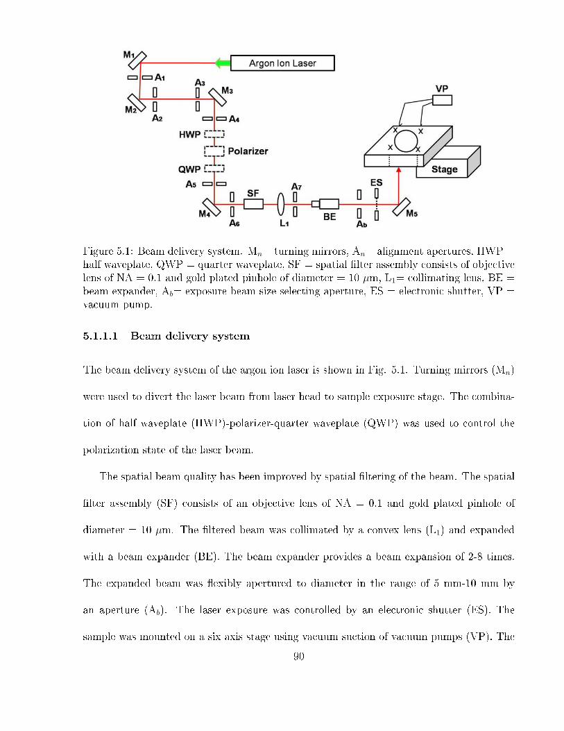
Figure 5.1: Beam delivery system. Mn= turning mirrors, An= alignment apertures, HWP =half waveplate, QWP = quarter waveplate, SF = spatial �lter assembly consists of objectivelens of NA = 0.1 and gold plated pinhole of diameter = 10 µm, L1= collimating lens, BE =beam expander, Ab= exposure beam size selecting aperture, ES = electronic shutter, VP =vacuum pump.
5.1.1.1 Beam delivery system
The beam delivery system of the argon ion laser is shown in Fig. 5.1. Turning mirrors (Mn)
were used to divert the laser beam from laser head to sample exposure stage. The combina-
tion of half waveplate (HWP)-polarizer-quarter waveplate (QWP) was used to control the
polarization state of the laser beam.
The spatial beam quality has been improved by spatial �ltering of the beam. The spatial
�lter assembly (SF) consists of an objective lens of NA = 0.1 and gold plated pinhole of
diameter = 10 µm. The �ltered beam was collimated by a convex lens (L1) and expanded
with a beam expander (BE). The beam expander provides a beam expansion of 2-8 times.
The expanded beam was �exibly apertured to diameter in the range of 5 mm-10 mm by
an aperture (Ab). The laser exposure was controlled by an electronic shutter (ES). The
sample was mounted on a six axis stage using vacuum suction of vacuum pumps (VP). The
90

Figure 5.2: The photograph of the actual experimental beam delivery system. Importantcomponents have been labeled.
photograph of the actual experimental setup has been shown in Fig. 5.2 with key components
labeled.
5.1.1.2 Beam pro�le
For generating a uniform 3D near-�eld di�raction pattern, ideally a �top-hat� exposure laser
beam pro�le is required. Unfortunately, the argon-ion laser used in this research, was ex-
tremely non-ideal with many hot spots on beam pro�le as can be seen in Fig. 5.3a and
in corresponding single line intensity distribution in Fig. 5.3b. The laser beam pro�le was
measured in front of the laser head before M1 mirror as depicted in Fig. 5.1. The laser beam
was improved with spatial �ltering and subsequent beam expansion to mimic a top-hat beam
pro�le. Figure 5.3c shows the 2D beam pro�le and (d) the corresponding single line inten-
sity distribution after spatial �ltering. The beam pro�le was measured after aperture A7
with aperture A7 set at 5 mm diameter. The beam was further expanded by 4 times with
a beam expander (BE) and the expanded beam was apertured with the aperture Ab of 10
91
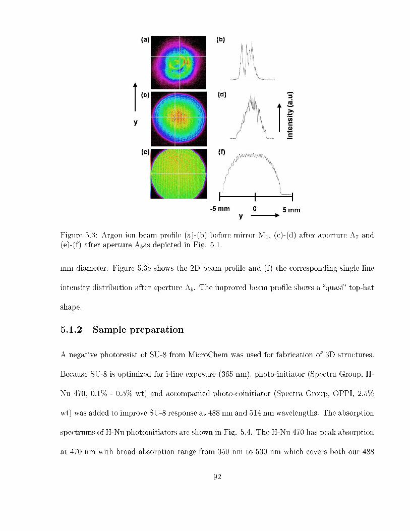
Figure 5.3: Argon ion beam pro�le (a)-(b) before mirror M1, (c)-(d) after aperture A7 and(e)-(f) after aperture Abas depicted in Fig. 5.1.
mm diameter. Figure 5.3e shows the 2D beam pro�le and (f) the corresponding single line
intensity distribution after aperture Ab. The improved beam pro�le shows a �quasi� top-hat
shape.
5.1.2 Sample preparation
A negative photoresist of SU-8 from MicroChem was used for fabrication of 3D structures.
Because SU-8 is optimized for i-line exposure (365 nm), photo-initiator (Spectra Group, H-
Nu 470, 0.1% - 0.5% wt) and accompanied photo-coinitiator (Spectra Group, OPPI, 2.5%
wt) was added to improve SU-8 response at 488 nm and 514 nm wavelengths. The absorption
spectrums of H-Nu photoinitiators are shown in Fig. 5.4. The H-Nu 470 has peak absorption
at 470 nm with broad absorption range from 350 nm to 530 nm which covers both our 488
92

Figure 5.4: Absorption of H-Nu photoinitiators.
nm and 514 nm laser wavelengths. Other two H-Nu photoinitiators, H-Nu 535 and H-Nu
635 have peak absorption at 535 nm and 635 nm respectively.
A uniform 15-30 µm thick resist layer was spun onto glass substrates. The sample was
soft baked and exposed with argon ion laser light. Detailed sample preparation is given in
Appendix-B.
5.1.3 Post exposure baking and development
Laser exposure of the photoresist was followed by two steps of post-exposure baking (3 min
at 65oC and 5 min at 95oC) to complete the polymerization process. The baked sample was
naturally cooled to room temperature and then processed with SU-8 developer for 10 min.
The developed sample was rinsed with isopropanol (IPA) and dried with nitrogen gas. The
93

SU-8 photoresist shrinks after development which is an unfortunately common problem with
thick SU-8 photoresist. A wide range of SU-8 shrinkage between 5%-15% has been reported
in literature [35,43,57] which depends on photoresist preparation, post exposure baking and
development process [57].
5.1.4 Characterization
Three-dimensional nanostructures are characterized in two steps. First they are characterized
structurally to assess quality of the 3D structure. Subsequently, good quality 3D structures
are probed optically for stopgap measurement.
5.1.4.1 Structural characterization
To ascertain periodicity along all three dimensions, the top as well as the cross-sectional
views of the structure need to be evaluated. Due to sub-micron feature sizes, a scanning
electron microscope was used. For cross-sectional view, the 3D structures were cleaved by
scratching the substrate with diamond-cutter and breaking the sample along the scratch line
using manual force. The manually cleaved sample was mounted vertically for cross-sectional
SEM. In special circumstances for clean cleaving of 3D structures, focused ion beam (FIB)
was used for in-situ milling and observation of the structure using a FIB/SEM combination
in the Nanofabrication facility of University of Western Ontario.
A. SEM
The SEM (SEM, Hitachi S-5200) images were taken in Centre for Nanostructure Imaging
facility of University of Toronto. For top view, the sample was mounted horizontally on
a SEM stub using carbon paste. Polymer samples were manually cleaved and mounted
94
vertically for cross-sectional SEM observation. Due to low conductivity, the polymer SU-
8 structures were carbon coated before SEM. For carbon coating a high vacuum carbon
coater was used (Emitech High vacuum Carbon coater). A thin layer (300-400 Å) of carbon
was deposited on the polymer sample following 60 sec - 90 sec evaporation time for a set
evaporation current of 16-17 ampere. For better electron mobility, a conductive contact is
made between deposited carbon layer and metal SEM stub using a tiny amount of carbon
paste. During SEM a 1kV voltage and 20-25 µA emission current was used for imaging of
the polymer structure.
B. FIB
Ideally all 3D structures should be milled with FIB for smooth high quality cross-sectional
views. Manual cleaving creates irregularities and distortions of the cross-sectional SEM
image of the structure. However, in this research, only silica inverted structures were milled
with FIB at University of Western Ontatio.
5.1.4.2 Optical characterization
A. Near-infrared transmission measurement
Samples were probed along the Γ-Z direction (normal incidence) with a fourier transform
infrared (FTIR) spectrometer (Bruker, Tensor 27) in the 1.4-µm to 5-µm spectral range.
The 10 mm diameter beam size of the FTIR, was apertured to 1 mm beam diameter for
probing 3D samples. All spectral recordings were normalization against a reference spectrum
recorded through an identical substrate coated with a fully developed solid resist coated to
same thickness of the sample.
95

B. Telecom band transmission measurement
Transmission spectra were recorded in the 1.25µm to 1.65 µm spectral range on a �ber-to-
�ber U-bench using a broadband light source (Agilent, 83437A) collimated to 500-µm diam-
eter (1/e2 intensity), a rotatable sample mount, and an optical spectrum analyzer (Ando,
AQ6317B). All spectral recordings were normalization against a reference spectrum recorded
through an identical substrate coated with a fully developed solid resist coated to the same
thickness of the sample.
96

Chapter 6
Fabrication using one-dimensional
di�ractive optics
6.1 Introduction
Our group was �rst to extend DOEs to the fabrication of 3D photonic crystal templates,
creating diamond-like woodpile structures in SU-8 photoresist by two sequential exposures
of orthogonal one-dimensional DOEs (1D-DOE) with an Ar-ion laser [15,43,53]. The present
chapter builds on this sequential DOE-exposure method [43, 58] by improving the fabrica-
tion precision of woodpile photonic crystal templates and, for the �rst time, spectroscopically
characterizing the templates to verify their 3D structure against energy band models. Thick,
large-area periodic nano-structures are con�rmed to have woodpile structure closely match-
ing the computed optical interference iso-intensity surfaces. However, imprecise alignment
between two DOE exposures prevents this method from reproducibly interlace two 2D struc-
tures and a single exposure DOE method is therefore preferred for improved uniformity and
reproducibility of the 3D structure. The phase-tunable DOE has enabled DOE formation
of 3D photonic crystal templates with a single laser exposure. The controlled separation
of the two optical elements provided a variable phase shift to manipulate the interlacing
97

position of two orthogonally rotated periodic structures, and thereby facilitate fabrication of
diamond-like woodpile structures having tetragonal (TTR) symmetry through to structures
we predict to have body-centered-tetragonal (BCT) symmetry, and including variations in
between. Finite di�erence time domain (FDTD) calculation of interference patterns and
associated isointensity surfaces are corroborated by de�nitive demonstrations of TTR and
BCT symmetry structures inside photoresist that smoothly transform from TTR to BCT
symmetry by the DOE phase shift.
The spectroscopic characterization of these templates reveals numerous low and high
energy stopbands along preferential crystallographic directions that are consistent with cal-
culated band dispersion curves for the low-index media. The results demonstrate good struc-
tural uniformity through a relatively large resist thickness and over large exposure area.
6.2 One-dimensional DOE for double laser exposure method
6.2.1 Laser exposure setup
In our initial work we have used a 1D-DOE which creates a 2D log-pile type near-�eld
di�raction pattern. To create a 3D periodic structure, the �rst 1D-DOE exposure is followed
by a second exposure with an identical but orthogonal 1D-DOE, creating the rotated 2D
log-pile intensity pattern. Between two laser exposures a high precision motion control stage
is used to move one DOE mask with respect to the sample surface (nr) to interlace two 2D
structures with quarter period shift (S = c/4) along the optical axis as shown in Fig. 6.1.
The combination of two sequential exposures then yields an intensity pattern described by
the interlaced diamond-like woodpile structure as discussed in Section 4.4.1 of Chapter 4.
To facilitate translation between two 1D DOEs using a x-motion stage as well as axial shift
98

Figure 6.1: Double laser exposure based diamond-like woodpile photonic crystal fabricationtechnique.
using a z-motion stage, an air gap (ni= 1.0) is maintained between DOE and sample surface.
6.2.2 Fabrication of 3D woodpile structures
Three-dimensional woodpile templates were patterned into photoresist by two sequential
exposures of a cw argon ion laser at 488-nm wavelength through two orthogonal 1D-DOEs,
each a linear phasemask with Λ = 1.066 µm period. Photo-initiator was added (0.1 wt %)
to improve SU-8 response at 488 nm. A uniform 15 µm thick resist layer was spun onto glass
substrates following the recipe discussed in Appendix-A. Periodic structures of a = 1.066
µm and c = 7.29 µm were expected inside the negative photoresist according to Eq. (3.4).
To avoid surface damage, an ∼0.2 mm air gap was maintained between the DOE and the
photoresist during alignment and exposure. Two consecutive 1D-DOE exposures produced
interlaced orthogonal log patterns with shift S = c/4 to create the woodpile structure as
predicted in Section 4.4.1. A 5-second exposure was applied through each 1D-DOE at 650
99

Figure 6.2: Top SEM view (a) of the DOE fabricated 3D photonic crystal template togetherwith cross-sectional view (b), showing 9 layers in the SU-8 photoresist. Inset (ii) showsmagni�ed version of cross-section and inset (i) and inset (iii) shows interference equationbased iso-intensity surface predictions.
mW power over 3 mm diameter (full-width half maximum, FWHM) laser exposure area which
was followed by two steps of post-exposure baking of the resist to complete the polymerization
process after laser exposure. Fig. 6.2 shows the scanning electron beam microscope images
of the top view (a) and cross-sectional view (b) of the photoresist after two orthogonal DOE
exposures and development. A woodpile 3D photonic crystal structure is clearly evident
with lateral periodicity of a ≈ 1.05 µm and axial periodicity of c ≈ 6.27 µm.
Because the photoresist is bonded to the glass substrate, there is little lateral shrinkage
(∼1%) of the resist as the observed lateral period (a ≈ 1.05 µm) closely matches the Λ =
1.066 µm grating period as predicted by Eq. (3.4). On the other hand, the axial period
(c = 6.27 µm) is 14% smaller than the expected c = 7.29µm value, which is attributed
to resist shrinkage during development, an unfortunately common problem with thick SU-8
photoresist [43,59]. The cross-sectional view in Fig. 6.2b shows uniform structure formation
across the full 13 µm thickness of the developed photoresist, supporting our assertion that
the DOE method can produce thick photonic crystal templates in photosensitive materi-
100
als. A 3D periodic structure extended fully across the ∼2000µm diameter exposure area.
Iso-intensity surface calculations were carried out as brie�y described in Section 3.5.2.1 to
match the observed SEM structure and are shown overlaid as inset (i) and (iii) in Fig. 6.2.
Resist shrinkage was taken into account in the simulation by anisotropic scaling by a 14%
axial shrinkage factor. The SEM observations are accurately replicated by the iso-intensity
calculations over a large sample area. The SEM in Fig. 6.2b-(ii) provides values of Rx =
0.23 µm, Rz = 1.45 µm ≈ c/4.32 and S = 1.55 µm ≈ c/4.05. These values satisfy the
interlacing conditions of Eq. (4.1) for formation of a stable, interconnected 3D structure.
The SEM images provide an estimated �lling fraction of f ≈ 69%, which closely corresponds
with the f ≈ 64% value used to optimize the iso-intensity pro�le matching in Fig. 6.2. The
interlacing o�set, S, was di�cult to control to c/4 precision across the full surface area of the
photoresist using our present alignment stages. However, a slight non-parallel alignment (<
10 mrad) was introduced between the two DOE surfaces to slowly varying the S o�set across
the 3-mm diameter (FWHM) laser exposure area which created a wide range of non-perfect
(S 6= c/4) log-pile structures. The fabricated 3D structure was found to be smooth over
large sample area (∼2000 µm diameter) with minimum resolvable feature size of ≤200 nm.
The surface morphology is relatively smooth with roughness of ∼10 nm that suggest low
optical scattering loss. The slight tilting of the structure (Fig. 6.2b) has been attributed to
lateral shrinkage of the top layer relative to a bonded (non-shrinking) bottom layer. With
the present DOEs, various �lling fractions could be reproducibly created by varying the
exposure time (3 to 15 seconds) and laser power.
101

6.3 Phase tunable DOE for single exposure method
To overcome the inherently imprecise DOE alignment that arises between two laser expo-
sures, a single laser exposure fabrication of 3D photonic crystals is highly desirable. In the
�rst proposed method, back-to-back mounting of two commercial linear phasemasks with
crossed grating orientation de�ned a phase-tunable DOE that permitted the fabrication of
the diamond-like structure. The schematic of the phase-tunable DOE arrangement is shown
in Fig. 6.3a. By simply tuning the phase di�erence of one set of �rst order di�racted beams
with the physical separation between the two di�ractive elements, a continuum of other
3D periodic structures that are tunable from the double basis diamond-like structure to a
single basis structure having body-centered-tetragonal symmetry (BCT) were fabricated as
described in Chapter 4.
6.3.1 Laser exposure setup
To improve fabrication reproducibility of diamond-like structure, a single-DOE device with
an appropriate �xed phase-shift was proposed as shown in Fig. 6.3. Photonic crystal tem-
plates were fabricated with the phase tunable DOE arrangement of Fig. 6.3, using two iden-
tical fused silica phasemasks having period Λ= 1.066 µm. The phase-tunable DOE further
o�ered formation of a continuum of other 3D periodic structures that were tunable from
the double basis diamond-like structure to a single basis structure having body-centered-
tetragonal symmetry (BCT) by simply tuning the phase di�erence (π/2 to 0 radian) of one
set of �rst order di�racted beams with the physical separation between the two di�ractive
elements [35].
The 3D laser near-�eld interference pattern was captured in a uniform photoresist layer,
102
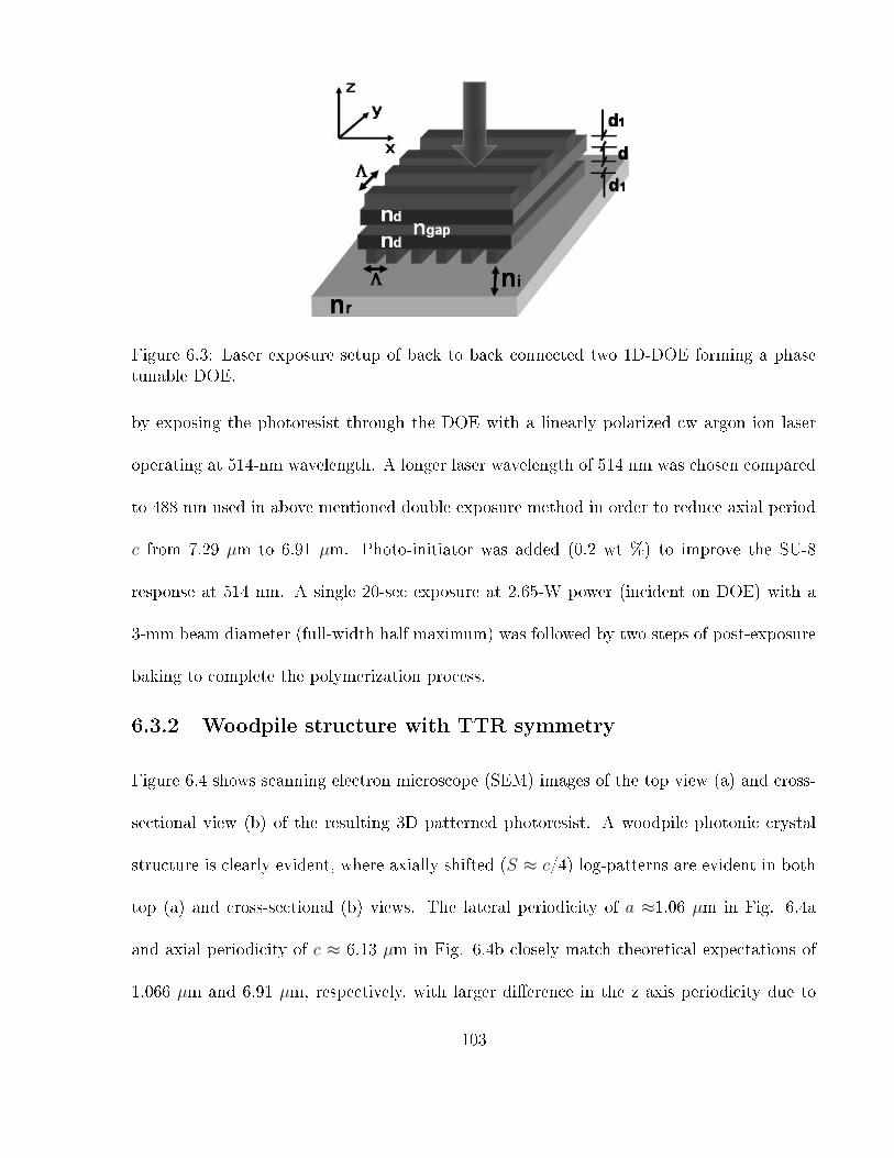
Figure 6.3: Laser exposure setup of back to back connected two 1D-DOE forming a phasetunable DOE.
by exposing the photoresist through the DOE with a linearly polarized cw argon ion laser
operating at 514-nm wavelength. A longer laser wavelength of 514 nm was chosen compared
to 488 nm used in above mentioned double exposure method in order to reduce axial period
c from 7.29 µm to 6.91 µm. Photo-initiator was added (0.2 wt %) to improve the SU-8
response at 514 nm. A single 20-sec exposure at 2.65-W power (incident on DOE) with a
3-mm beam diameter (full-width half maximum) was followed by two steps of post-exposure
baking to complete the polymerization process.
6.3.2 Woodpile structure with TTR symmetry
Figure 6.4 shows scanning electron microscope (SEM) images of the top view (a) and cross-
sectional view (b) of the resulting 3D patterned photoresist. A woodpile photonic crystal
structure is clearly evident, where axially shifted (S ≈ c/4) log-patterns are evident in both
top (a) and cross-sectional (b) views. The lateral periodicity of a ≈1.06 µm in Fig. 6.4a
and axial periodicity of c ≈ 6.13 µm in Fig. 6.4b closely match theoretical expectations of
1.066 µm and 6.91 µm, respectively, with larger di�erence in the z axis periodicity due to
103
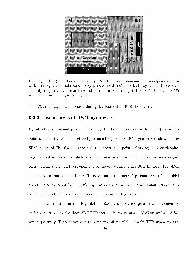
Figure 6.4: Top (a) and cross-sectional (b) SEM images of diamond-like woodpile structurewith TTR symmetry fabricated using phase-tunable DOE method together with insets (i)and (ii), respectively, of matching isointensity surfaces computed by FDTD for d = 2.725µm and corresponding to S = c/4.
an 11.3% shrinkage that is typical during development of SU-8 photoresist.
6.3.3 Structure with BCT symmetry
By adjusting the mount pressure to change the DOE gap distance (Eq. (4.8)), one also
obtains an e�ective S = 0 o�set that produces the predicted BCT symmetry as shown in the
SEM images of Fig. 6.5. As expected, the intersection points of orthogonally overlapping
logs manifest in cylindrical photoresist structures as shown in Fig. 6.5a that are arranged
on a periodic square grid corresponding to the top surface of the BCT lattice in Fig. 4.9a.
The cross-sectional view in Fig. 6.5b reveals an inter-penetrating square-grid of ellipsoidal
structures as expected for this BCT symmetry structure with no axial shift between two
orthogonally rotated logs like the woodpile structure in Fig. 6.4b.
The observed structures in Fig. 6.4 and 6.5 are directly comparable with isointensity
surfaces generated by the above 3D FDTD method for values of d = 2.725 µm and d = 3.634
µm, respectively. These correspond to respective o�sets of S = c/4 for TTR symmetry and
104

Figure 6.5: Top (a) and cross-sectional (b) SEM images of structure with BCT symmetryfabricated using phase-tunable DOE method together with insets (i) and (ii), respectively,of matching isointensity surfaces computed by FDTD for d = 3.634µm and correspondingto S = c.
S = 0 for BCT symmetry and yield the isointensity surfaces overlaid as inset (i) and (ii) in
the respective top and cross-sectional views in both Fig. 6.4 and 6.5. It can be observed
that isointensity calculations very closely match the SEM observations of both structures.
6.3.4 Fabrication of diamond-like structure with circularly polar-
ized light
In the previous section, we reported fabrication of diamond-like structures using linearly
polarized light for the DOE parameters given above. Because of polarization dependence,
the relative measured di�raction e�ciencies (ηmn) of 1st order to 0th order beam η01/η00 =
η0−1/ η00 ∼ 3 along the z-x plane and η10/ η00= η−10/ η00 ∼ 4 along the z-y plane for DOE
grove depth dt = 265 nm resulted in a non-symmetric 3D intensity distribution between z-x
and z-y planes. Circular polarization eliminates this polarization dependence in this case
by balancing di�raction e�ciencies ratios to η10/η00 = η−10/η00 = η01/ η00= η0−1/ η00 ≈3.5
which consequently produces symmetric intensity distribution compared to linearly polarized
105

Figure 6.6: Top (a) and cross-sectional (b) SEM images of diamond-like woodpile structureshaving TTR symmetry together with insets (i) and (ii), respectively, of corresponding in-tensity distribution (<I(x,y)>) computed by FDTD for d = 2.725 µm air gap between twophasemasks corresponding to shift S = c/4.
light. The key to obtain symmetric intensity distribution is to ensure equal di�raction
e�ciency of all 1st order beams which is automatically guaranteed by circular polarization
for this DOE arrangement of two identical phasemasks.
Scanning electron microscope images of the top view (a) and cross-sectional view (b) of
the resulting 3D patterned photoresist is shown in Fig. 6.6 for shift S = c/4. A diamond-like
woodpile photonic crystal structure is clearly evident, where axially shifted (S ≈ c/4) log-
patterns are manifested in both top (a) and cross-sectional (b) views. The lateral periodicity
of a ≈ 1.06 µm in Fig. 6.6a and axial periodicity of c ≈ 6.21 µm in Fig. 6.6b closely matches
theoretical predictions of a = 1.066 µm and c = 6.91 µm, respectively, with larger di�erence
in the z axis periodicity due to a 10.1 % shrinkage. The observed structure in Fig. 6.6
is directly comparable with the intensity distribution (<I(x, y, z)>) predicted by the 3D
FDTD calculation for values of d = 2.725 µm corresponding to shift S = c/4, and overlaid
as inset (i) and (ii) in the top and cross-sectional views in Fig. 6.6 which very closely match
the SEM observations of the fabricated structure.
106

With circularly polarized light, the fabricated 3D structure was found to be more sym-
metric between z-x and z-y planes and more uniform over larger sample area (∼2-3 mm
diameter) compared to the structures made by linearly polarized light as reported in the
Section 6.3.2. Moreover, uniformity of all 1st order di�racted beams for circularly polarized
light o�ers better control of local laser exposure dose.
6.4 Optical characterization
Although the refractive index of the photoresist (nr = 1.6) is too small to create a wide
photonic bandgap, stopbands are predicted from numerical band calculation along several
crystallographic directions for woodpile structure. However, no such stopbands are predicted
for single basis BCT symmetry structure. In both 1D-DOE based double and single exposure
methods, DOE period of Λ = 1.006 µm was used which resulted in similar lateral and
axial periods of woodpile structures having similar optical characteristics. Here only optical
characterizations of woodpile structure fabricated using the double laser exposure method is
presented.
6.4.1 Near-infrared characterization
The woodpile structure shown in Fig. 6.2 was probed along the Γ-Z direction (c axis in Fig.
6.2b for TTR symmetry) with a Fourier transform infrared (FTIR) spectrometer in the 1.4-
µm to 5-µm spectral range. All spectral recordings were normalization against a reference
spectrum recorded through an identical substrate coated with a fully developed solid resist
coated to similar 13-µm thickness. The normalized transmission spectrum of the structure
is shown in Fig. 6.7b. A strong absorption trough from 2.6 to 3.6 µm has been attributed
107
to intrinsic material absorption by the SU-8 �lm. Outside this band, a moderately strong
stopband is noted at 4.45-µm wavelength that we attribute to a Γ-Z direction stopband,
together with several higher-order bands near 2 to 3 µm. Di�raction losses due to the a
= 1.05 µm periodic planar structure are only possible for λ < 1.45 µm. A narrow ∼45-
nm (FWHM) bandwidth indicates that all 9 layers seen in Fig. 6.2b are acting coherently.
Hence, the DOE method of laser interference appears robust in replicating identical multi-
layer periodic structures deeply throughout the resist. The band dispersion relation for
this structure was calculated from the isointensity surface of Fig. 6.2 and is shown in Fig.
6.7a. This isointensity surface had been computed iteratively to match the SEM contours,
the periodicity, and the ratio c/a = 6.27/1.05 = 5.97 observed in the fabricated structure.
The computed �lling fraction of f = 64% corresponds well with the approximate f ≈ 69%
value estimated from the SEM cross-sections. The observed stop band at 4.45 µm closely
matches the predicted stopband at 4.62 µm (a /λ = 0.2273) in the Γ-Z direction of the
energy dispersion curve as identi�ed by the two horizontal lines crossing both �gures. The
predicted bandwidth of ∼58 nm slightly exceeds the observed ∼45 nm (FWHM) bandwidth.
These mismatches can be readily attributed to uncertainties in estimating the structural
shrinkage, the �lling fraction, the motif, and the refractive index of SU-8 (nr=1.6). The
spectral response of the stopband was nearly invariant over relatively large sample area
(∼2000 µm diameter) con�rming the good structural uniformity of the photonic crystal over
the large exposure area. Figure 6.7a further reveals several narrow higher order bandgaps are
also predicted in the band calculation, which however we could not be de�nitively assigned
to the spectroscopic observations in Fig. 6.7b at the present time.
108
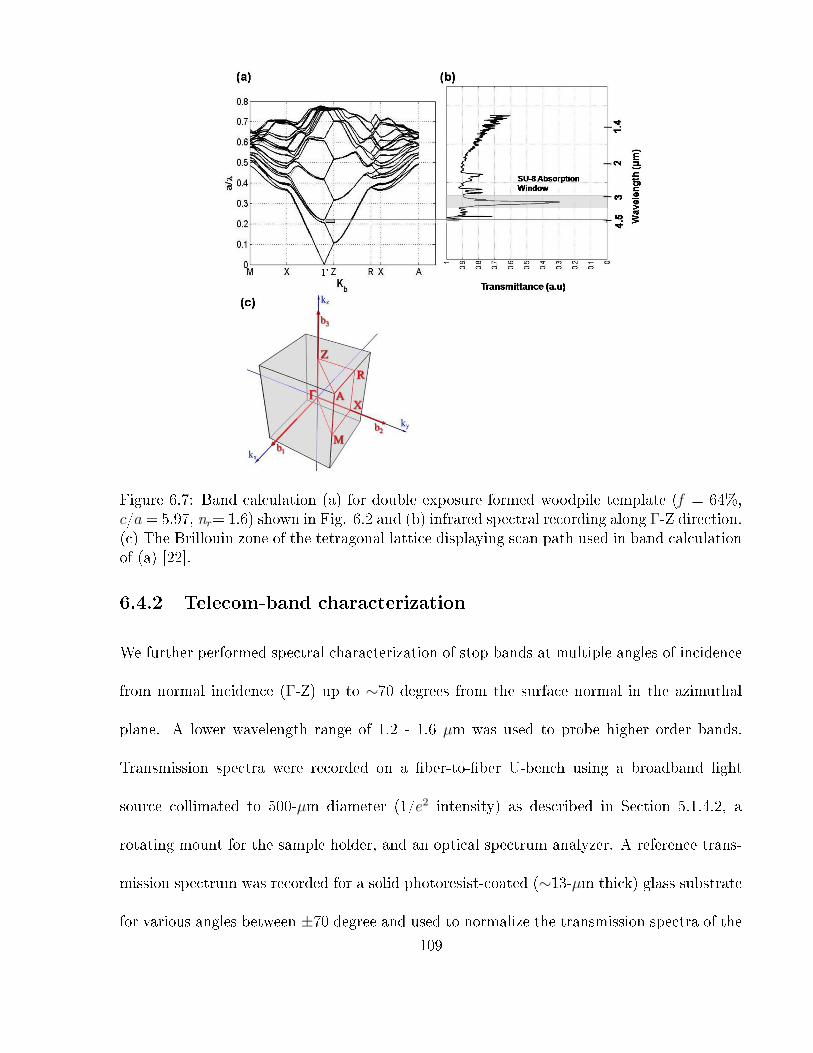
Figure 6.7: Band calculation (a) for double exposure formed woodpile template (f = 64%,c/a = 5.97, nr= 1.6) shown in Fig. 6.2 and (b) infrared spectral recording along Γ-Z direction.(c) The Brillouin zone of the tetragonal lattice displaying scan path used in band calculationof (a) [22].
6.4.2 Telecom-band characterization
We further performed spectral characterization of stop bands at multiple angles of incidence
from normal incidence (Γ-Z) up to ∼70 degrees from the surface normal in the azimuthal
plane. A lower wavelength range of 1.2 - 1.6 µm was used to probe higher order bands.
Transmission spectra were recorded on a �ber-to-�ber U-bench using a broadband light
source collimated to 500-µm diameter (1/e2 intensity) as described in Section 5.1.4.2, a
rotating mount for the sample holder, and an optical spectrum analyzer. A reference trans-
mission spectrum was recorded for a solid photoresist-coated (∼13-µm thick) glass substrate
for various angles between ±70 degree and used to normalize the transmission spectra of the
109

woodpile samples. Aside from di�erences in Fresnel losses, no angular dependence e�ects
were observed in the reference sample spectra. The normalized transmission spectra of the
woodpile structure are plotted in Fig. 6.8 for various incident angles between 0 Deg and
24 Deg. High transmission with relatively �at spectral response was noted for all angles
from 0 Deg to 16 Deg. Three strong attenuation troughs started to appear around 16 Deg
angle of incidence at ∼1280 nm, 1397 nm and 1541 nm with spectral spacing of 117 nm
and 144 nm, respectively. The spectral attenuation increases monotonically with angle from
the approximate -1-dB baseline at 16 Deg to a peak value of approximately -22 dB at ∼21
Deg. With further increase in angle of incidence, the attenuation diminishes and a �at high
transmission spectrum is found again at ∼25 Deg, which continues to remain high up to
angle 70 Deg. As expected due to the crystal symmetry, the spectra follow similar angular
dependence at negative angles of incidence as well. The spectral resonances are not due
to Fabry-Perot resonances which would generate a much smaller free-spectral range for the
13-µm thick photoresist on 1-mm thick glass substrates.
It is interesting to observe that these stopgaps are present only for a narrow angular
range. Given the a ≈ 1.05-µm lattice constant and λ =1.2 - 1.6 µm probing range, the range
of a/λ ≈ 0.84 - 0.65 corresponds to higher order bands. However, small uncertainties in the
physical structure prevent su�ciently precise energy band calculations to permit de�nitive
band assignments to these higher energy stop bands which remain open for such narrow range
of angle. Nevertheless, the narrow angular resonances in Fig. 6.8 con�rm the formation of
a highly uniform 3D woodpile structure throughout the thick resist (13 µm) and over large
area (2 mm diameter), which would otherwise be washed out by minor lattice distortions for
such high-order bands. Such narrow angle spectral sensitivity can be exploited for various
110
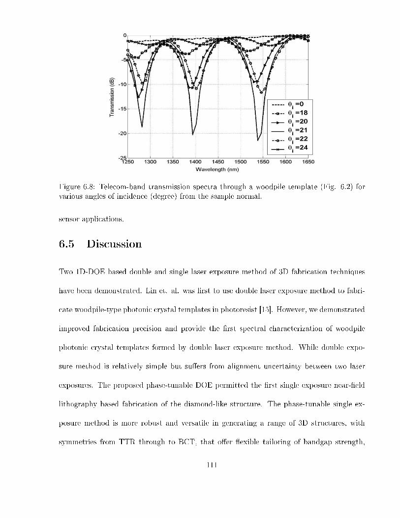
Figure 6.8: Telecom-band transmission spectra through a woodpile template (Fig. 6.2) forvarious angles of incidence (degree) from the sample normal.
sensor applications.
6.5 Discussion
Two 1D-DOE based double and single laser exposure method of 3D fabrication techniques
have been demonstrated. Lin et. al. was �rst to use double laser exposure method to fabri-
cate woodpile-type photonic crystal templates in photoresist [15]. However, we demonstrated
improved fabrication precision and provide the �rst spectral characterization of woodpile
photonic crystal templates formed by double laser exposure method. While double expo-
sure method is relatively simple but su�ers from alignment uncertainty between two laser
exposures. The proposed phase-tunable DOE permitted the �rst single exposure near-�eld
lithography based fabrication of the diamond-like structure. The phase-tunable single ex-
posure method is more robust and versatile in generating a range of 3D structures, with
symmetries from TTR through to BCT, that o�er �exible tailoring of bandgap strength,
111

width, and spectral dispersion. A relatively long period DOEs (Λ = 1.066 µm) provided 3D
templates in SU-8 photoresist that con�rm formation of thick, large area periodic nanostruc-
tures with closely matched to optical interference isointensity predictions.
The present combination of DOE period (Λ = 1.066 µm), laser wavelength (λd = 514
nm) and photoresist (nr = 1.6) produced a large c/a ≈ 6.48 ratio that is not ideal for
producing a complete photonic bandgap when inverted with a high refractive index materi-
als. DOE designs that can generate ideal lattice constants and �lling fraction for woodpile
structure which will provide a complete bandgap are described in Section 4.3. Nevertheless,
the spectroscopic characterization of the templates revealed numerous low and high energy
stopbands along preferential crystallographic directions that were consistent with calculated
band dispersion curves for the low-index media. The SEM and spectral observations show
good structural uniformity through a relatively large resist thickness and over large exposure
area that promise 3D photonic crystal devices with high optical quality.
112

Chapter 7
Fabrication using two-dimensional
di�ractive optics
7.1 Introduction
As introduced in Chapter 6, a woodpile structure was �rst formed with di�ractive optic near-
�eld lithography by two sequential laser exposures of photoresist using orthogonally rotated
1D binary phasemasks. To overcome the inherently imprecise DOE alignment that arises
between two laser exposures, a single laser exposure fabrication of 3D photonic crystals was
devised by back-to-back mounting of two linear phasemasks with crossed grating orientation.
Although, the phase tunable near-�eld DOE method was versatile, it required accurate
physical separation of the two orthogonally rotated gratings in order to provide a precise
c/4 shift between two orthogonal interference patterns required for diamond-like woodpile
structure. To improve fabrication reproducibility of diamond-like structure, a single 2D DOE
device with an appropriate �xed phase-shift is therefore highly desirable. While John and co-
workers proposed a phasemask design based on orthogonal placement of linear phasemasks
on opposite surfaces of a single DOE substrate [56], this design requires tedious etching
and deposition processes on opposite surfaces of a substrate as well as precise control of
113

separation between two the 1D gratings.
In this chapter, we present a single-surface multi-level 2D DOE design with locked-in
phase-shift optimized for formation of diamond-like photonic crystal structure in a single
laser exposure step. Rather than rely on the precise control of substrate thickness [56], or
the accurate physical separation of two DOEs for phase control [35], a phase shift was built
into the single-surface DOE design which further also enabled ease of etching of di�ractive
elements on single side of a substrate. Here, the proposed multi-level DOE was laser fab-
ricated on a thin polymer �lm to generate a woodpile near-�eld intensity distribution with
much smaller periodicity (a = b = 650 nm and c = 2.46 µm) over our prior demonstrations
(a = b = 1.06 µm and c = 6.91 µm) as described in Chapter 6. The DOE was then applied to
form diamond-like structures were fabricated in photoresist having Γ-Z (normal incidence)
stopbands now shifted into the 1.25-1.65 µm telecom band from previous observations in the
3 to 5 µm spectral range.
7.2 Fabrication of two-dimensional di�ractive optics
To demonstrate the e�ect of 2D DOE phase levels a two-level DOE was �rst custom designed
and commercially fabricated using standard semiconductor lithography, and applied to fab-
ricate a single basis BCT symmetry structure. The proposed three-level DOE was fabricated
by two photon polymerization with a femtosecond laser and the three-level photoresist mask
was used to fabricate a woodpile structure.
114
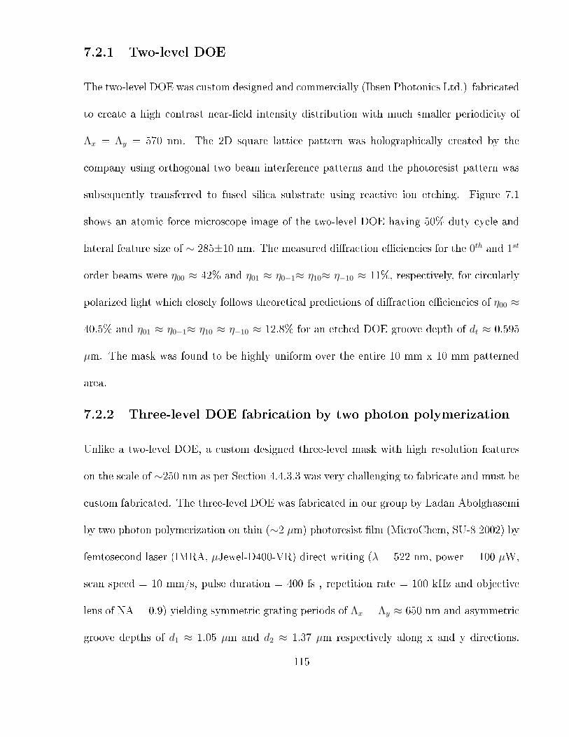
7.2.1 Two-level DOE
The two-level DOE was custom designed and commercially (Ibsen Photonics Ltd.) fabricated
to create a high contrast near-�eld intensity distribution with much smaller periodicity of
Λx = Λy = 570 nm. The 2D square lattice pattern was holographically created by the
company using orthogonal two beam interference patterns and the photoresist pattern was
subsequently transferred to fused silica substrate using reactive ion etching. Figure 7.1
shows an atomic force microscope image of the two-level DOE having 50% duty cycle and
lateral feature size of ∼ 285±10 nm. The measured di�raction e�ciencies for the 0th and 1st
order beams were η00 ≈ 42% and η01 ≈ η0−1≈ η10≈ η−10 ≈ 11%, respectively, for circularly
polarized light which closely follows theoretical predictions of di�raction e�ciencies of η00 ≈
40.5% and η01 ≈ η0−1≈ η10 ≈ η−10 ≈ 12.8% for an etched DOE groove depth of dt ≈ 0.595
µm. The mask was found to be highly uniform over the entire 10 mm x 10 mm patterned
area.
7.2.2 Three-level DOE fabrication by two photon polymerization
Unlike a two-level DOE, a custom designed three-level mask with high resolution features
on the scale of ∼250 nm as per Section 4.4.3.3 was very challenging to fabricate and must be
custom fabricated. The three-level DOE was fabricated in our group by Ladan Abolghasemi
by two photon polymerization on thin (∼2 µm) photoresist �lm (MicroChem, SU-8 2002) by
femtosecond laser (IMRA, µJewel-D400-VR) direct writing (λ = 522 nm, power = 100 µW,
scan speed = 10 mm/s, pulse duration = 400 fs , repetition rate = 100 kHz and objective
lens of NA = 0.9) yielding symmetric grating periods of Λx = Λy ≈ 650 nm and asymmetric
groove depths of d1 ≈ 1.05 µm and d2 ≈ 1.37 µm respectively along x and y directions.
115

Figure 7.1: Atomic force microscope image of the two-level DOE of period Λx = Λy = 570nm and etch depth dt = 595 nm. Inset (i) show single-line height pro�le that de�ne groovedepths dt (Length of scale bars as indicated).
Precise depth control (∼330 nm) and parallel alignment to the substrate was aided by a
high precision air-bearing motion stage (Aerotech Inc., ABL1000-3D).
Figure 7.2 shows an atomic force microscope (AFM) image of the three-level DOE fab-
ricated by femtosecond laser direct writing after laser exposure and development. The 2D
periodic structure was found to be uniform over most of the direct laser written area of 5
mm x 5 mm. Three di�erent phase levels of the DOE are represented by three false colors
representing asymmetric groove depths of d1 ≈ 1.05 µm and d2 ≈ 1.37 µm, respectively,
along x and y directions. The inset (i) and (ii) in Fig. 7.2 show the d2 and d1 surface
pro�les along a-c and c-d phase segments, respectively, of an unit cell shown in inset (iii).
The di�erence in DOE groove depths (d2- d1) ≈ 320 nm closely satis�es Eq. (4.9) for a
shift S ≈ c/3.86 reduced to �rst phase shift zone of 0 ≤ S ≤ c/4. Because of higher net
laser exposure in the DOE line crossing points, an approximate ±20 nm height modulation
results along the a-b groove direction as seen in the unit cell shown in Fig. 7.2-(iii). This
116

deviates from the uniform phase pro�le expected as shown in the A-B section of the unit cell
of Fig. 7.2-(iv), leading to an unbalance of the di�raction orders. The measured di�raction
e�ciencies for the 0th and 1st order beams were η00 ≈ 48%, η01 ≈ η0−1 ≈ 15% and η10 ≈ η−10
≈ 8%, respectively, for circularly polarized light which closely follows theoretical predictions
of di�raction e�ciencies of η00 ≈ 56.7% and η01 ≈ η0−1 ≈ 13.7% and η10 ≈ η−10 ≈ 5.29%
for the inferred DOE groove depths of d1 ≈ 1.05 µm and d2 ≈ 1.37 µm determined by AFM
scan. This deviation from the targeted di�raction e�ciencies of η00 = 55% and η10 = η−10
= η01 = η0−1= 10% is attributed to the a-b modulation noted above and di�erences in the
fabricated groove depths d1 ≈ 1.05 µm and d2 ≈ 1.37 µm from design values of d1 = 1.13 µm
and d2 = 1.46 µm. This imbalance in di�raction order e�ciency as well as non-ideal phase
pro�le modi�ed the 3D near-�eld di�raction pattern. However, the strong step-function like
photoresist response mitigated these di�erences and hence the captured near-�eld pattern
inside the photoresist closely resembles the original predictions of the ideal DOE di�raction
pattern.
7.3 Single exposure fabrication of 3D photonic crystals
Figure 7.3 shows the laser exposure arrangement of (a) the two-level DOE shown in Fig. 7.1
and (b) the proposed three-level DOE shown in Fig. 7.2. Also shown the index matching
medium (ni) between the DOE substrate (ns) and photoresist (nr) layer which was spun
onto a substrate of refractive index ns. It is evident from the discussion in Section 4.3 that
high index materials (n > nr) are required to produce a highly symmetric (c/a ∼1) photonic
crystal template. For this reason, an index matching medium (ni) is proposed between the
DOE and photoresist in the laser exposure setup shown in Fig. 7.3. This allows propagation
117

Figure 7.2: Atomic force microscope image of the three-level DOE represented by the threedi�erent colors (heights). Enlarged section identi�es a unit cell abcd (iii) and the ideal heightpro�le ABCD (iv) used in the FDTD simulation. Inset (i) and (ii) show single-line heightpro�les in orthogonal scan directions that de�ne groove depths d2 and d1 (Length of scalebars as indicated).
of di�racted beams with larger di�raction angle which otherwise do not propagate in the air
gap between DOE and photoresist layer. This arrangement also further eliminates physical
contact and damage to the DOE by the photoresist.
7.3.1 Single basis BCT symmetry structure using two level DOE
Single basis BCT symmetry structures were fabricated with the two-level 2D DOE arrange-
ment of Fig. 7.3a. The 3D near-�eld di�raction pattern was captured in a uniform photoresist
layer, by exposing the photoresist through the DOE with a cw argon ion laser operating at
514-nm wavelength. Photo-initiator was added (0.5 wt %) to improve the SU-8 response at
514 nm. A single 12-sec exposure at 1.25-W power (incident on DOE) with a 10-mm beam
diameter (null-to-null) was followed by two steps of post-exposure baking to complete the
polymerization process. Figure 7.4 shows scanning electron microscope (SEM) images of the
top view (a) and cross-sectional view (b) of the resulting developed 3D patterned photoresist.
118

Figure 7.3: Laser exposure arrangement of a (a) two-level DOE and (b) the proposed three-level DOE showing index matching medium (ni) between DOE substrate (ns) and photoresist(nr) layer which is spun onto a substrate of refractive index ns.
A single basis BCT symmetry structure is clearly visible in Fig. 7.4. The lateral periodicity
of a ≈570 nm in Fig. 7.4(iii) and axial periodicity of c ≈1.54 µm in Fig. 7.4(iv) closely
match theoretical expectations of 570 nm and 1.84 µm, respectively, with larger di�erence
in the z axis periodicity due to an 16.3 % shrinkage during development of SU-8.
Due to weak connectivity between ellipsoidal motifs, the formation of a stable single basis
BCT symmetry structure is di�cult. Precise laser exposure dose is required to fabricate a
stable bi-continuous structure that also remains porous. In Fig. 7.4b, the 3D structure is
seen to form with high uniformity through the full ∼25 µm thickness of the photoresist,
forming 22 distinct layers. A highly connected stable BCT symmetry structure is clearly
visible in Fig. 7.4. The observed structure is directly comparable with isointensity surface
computed by the 3D FDTD. For FDTD calculation, measured DOE parameters given in
Section 7.2.1 were used. The resulting isointensity surfaces overlaid as inset (i) and (ii) in
the respective top and cross-sectional views in Fig. 7.4 are seen to very closely match the
SEM observations of the laser fabricated structure.
119

Figure 7.4: Top (a) and cross-sectional (c) SEM images of the BCT symmetry structure inSU-8 photoresist. Inset-(iii) and (iv) shows enlarged views of top and cross-section. Inset-(i)and (ii) shows corresponding predicted near-�led isointensity surfaces computed by FDTD.
7.3.2 Double basis diamond-like structure using three-level DOE
The woodpile three-dimensional photonic crystals were fabricated in photoresist by a single
exposure of a cw argon ion laser at 514-nm wavelength through the three-level DOE shown
in Fig. 7.2 and using the laser exposure arrangement of Fig. 4.12b [36, 60]. Photo-initiator
(H-NU 470, 0.2% wt of SU-8) was added to improve SU-8 absorption at 514 nm. A 7 second
exposure of photoresist (nr = 1.6) using a collimated 6-mm diameter (null-to-null) beam
of 3.15 W power was made in the arrangement of Fig. 4.12b through the index matching
�uid of refractive index ni = 1.604. This was followed by two steps of post-exposure baking
to complete the polymerization process. Figure 7.5 shows scanning electron microscope
images of the top view (a) and manually cleaved cross-sectional view (b) revealing 40 layers
120

Figure 7.5: Top (a) and manually cleaved cross-sectional (b) SEM images of diamond-likewoodpile structure in SU-8 photoresist showing 40 layers together with insets (i) and (iii),respectively, of predicted near-�led isointensity surfaces computed by FDTD. Inset (iv) showsenlarged view of cross-section of the actual structure and inset (ii) shows correspondingenlarged view of predicted isointensity surface of inset (iii) [36].
of the photoresist structure after exposure and development. A diamond-like woodpile 3D
photonic crystal structure is clearly evident with lateral periodicity of a ≈ 650±30 nm
and axial periodicity of c ≈ 2.32 ±75 µm, respectively, which closely match theoretical
expectations of a = 650 nm and c = 2.46 µm, respectively. The 6 % di�erence in the z axis
mean periodicity is due to shrinkage that is typical during development of SU-8, leading to a
smaller observed c/a value of 3.57 from the theoretical design ratio of c/a = 3.78. For a given
set of optimized parameters, usually 4-5 samples were made. These structures found to be
very similar. In some cases slight variation in �lling fraction was observed which possibly due
to a combination of causes like sample to sample minor variation of photo-initiator amount,
minor variation of laser exposure dose between exposures. We also observed small variation
in lattice constants. For the woodpile structure shown in Fig. 7.5, we measured 30 nm (std.
variation) of lateral period variation and 75 nm (std. variation) of axial period variation.
In Fig. 7.5b, the 3D structure is seen to form with high uniformity through the full
121

∼25 thickness of the photoresist, forming 40 distinct layers. Most of the irregularities and
distortions of the cross-sectional SEM image (Fig. 7.5b) of the structure came from the
damage during manual cleaving of the 3D soft polymer structure. By controlling laser
exposure dose, structures with a relatively wide range of �lling fraction or porosity have
been fabricated. Here, we intentionally chose the structure shown in Fig. 7.5 having a high
�lling fraction of ∼78% for its optical response in the telecom band as discussed in Section
7.4. A clear vertical o�set of S ≈ 0.605 µm is noted between the orthogonally rotated logs
in Fig. 7.5b-(iv) that closely matches the required ideal c/4 = 2.46/4 = 0.615 µm shift,
thus con�rming a double basis of a diamond-like structure. This corresponds well with the
shift S ≈ c/3.86 value inferred from Eq. (4.9) considering the periodic relation 0 ≤ S ≤
c/4 for the DOE groove depth di�erence of (d2- d1) ≈ 320 nm. The observed structure
in Fig. 7.5 is directly comparable with isointensity surfaces computed by the 3D FDTD
method, which was used to generate Fig. 4.15. For this calculation, the DOE unit cell
was approximated with rectangular phase elements as shown by inset (iv) in Fig. 7.2, but
using the measured AFM values of d1 ≈ 1.05 µm and d2 ≈ 1.37 µm inferred above. The
resulting isointensity surfaces overlaid as inset (i) and (iii) in the respective top and cross-
sectional views in Fig. 7.5 are seen to very closely match the SEM observations of the laser
fabricated structure. Inset (iv) shows an enlarged cross-sectional view of the photoresist
structure and inset (ii) shows the corresponding enlarged view of the predicted isointensity
surface of inset (iii). This close correspondence between FDTD predictions and fabricated
structures demonstrates the relatively high precision of femtosecond laser direct writing in
creating high resolution multi-level optical surfaces with �exible tailored designs for general
purpose fabrication of 3D periodic structures.
122
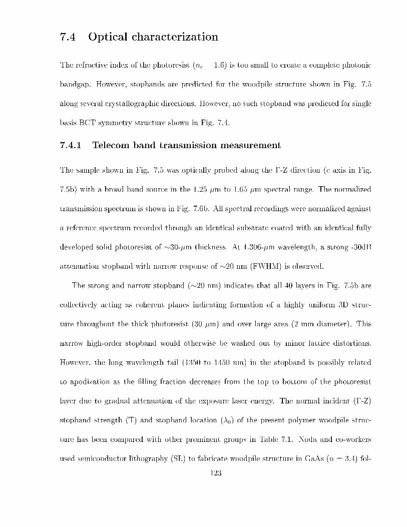
7.4 Optical characterization
The refractive index of the photoresist (nr = 1.6) is too small to create a complete photonic
bandgap. However, stopbands are predicted for the woodpile structure shown in Fig. 7.5
along several crystallographic directions. However, no such stopband was predicted for single
basis BCT symmetry structure shown in Fig. 7.4.
7.4.1 Telecom band transmission measurement
The sample shown in Fig. 7.5 was optically probed along the Γ-Z direction (c axis in Fig.
7.5b) with a broad band source in the 1.25 µm to 1.65 µm spectral range. The normalized
transmission spectrum is shown in Fig. 7.6b. All spectral recordings were normalized against
a reference spectrum recorded through an identical substrate coated with an identical fully
developed solid photoresist of ∼30-µm thickness. At 1.306-µm wavelength, a strong -30dB
attenuation stopband with narrow response of ∼20 nm (FWHM) is observed.
The strong and narrow stopband (∼20 nm) indicates that all 40 layers in Fig. 7.5b are
collectively acting as coherent planes indicating formation of a highly uniform 3D struc-
ture throughout the thick photoresist (30 µm) and over large area (2 mm diameter). This
narrow high-order stopband would otherwise be washed out by minor lattice distortions.
However, the long wavelength tail (1350 to 1450 nm) in the stopband is possibly related
to apodization as the �lling fraction decreases from the top to bottom of the photoresist
layer due to gradual attenuation of the exposure laser energy. The normal incident (Γ-Z)
stopband strength (T) and stopband location (λ0) of the present polymer woodpile struc-
ture has been compared with other prominent groups in Table 7.1. Noda and co-workers
used semiconductor lithography (SL) to fabricate woodpile structure in GaAs (n = 3.4) fol-
123

Figure 7.6: Band diagram (a) of the structure shown in Fig. 7.5 revealing a Γ-Z direc-tion (normal incidence) (c-axis) stopband between the 5th and 6th band and correspondingnormalized transmission spectrum (b) measured as normal angle of incidence through thestructure in Fig. 7.5b showing a strong (-30 dB) stopband at 1.306 µm.
lowing a layer-by-layer approach and observed a Γ-Z stopgap of -40dB at λ0= 1.3 µm [8].
Such strong stopband was observed due to high refractive index contrast (∆n = 2.4) of the
woodpile structure fabricated in GaAs. However, as expected comparatively weak stopband
was observed for polymer woodpile strutcure fabricated using direct laser writing (DLW) by
other three groups listed in the Table 7.1 [9, 10, 61]. The strong stopband (-30dB) observed
in the present work is attributed to the large number of layers (10 unit cells along the optical
axis) of the fabricated woodpile structure which strongly compensate for the low refractive
index contrast of the polymer-air structure.
7.4.2 Numerical band calculation
The band dispersion relation was numerically computed using the isointensity surface of the
fabricated structure shown in Fig. 7.5-(i)-(iii) using the numerical plane wave expansion
method described in Section 3.7.2. This isointensity surface had been computed iteratively
124

Table 7.1: Comparison of the normal incident (Γ-Z) stopband strength (T) and stopbandlocation (λ0) of the present polymer woodpile structure with woodpile structure fabricatedby other prominent groups.
Group Method a(µm) c(µm) c/a ∆n Layers λ0 (µm) T (dB)
Noda and co-workers [8] SL 0.7 0.84 1.2 2.4 8 1.3 -40
Present work [36] DOE 0.65 2.32 3.57 0.6 40 1.3 -30
Wegener and co-workers [9] DLW 1√
2√
2 0.6 12 1.7 -6
Chichkov and co-workers [61] DLW 1√
2√
2 0.56 8 1.6 -1
Misawa and co-workers [10] DLW 2 5.6 2.8 0.6 14 2.1 -0.1
to match the SEM contours, the periodicity, and the ratio c/a = 2.32/0.65= 3.57 observed in
the fabricated structure. The computed �lling fraction of f = 76.4% corresponds well with
the approximate f ≈ 78% value estimated from the SEM cross-sections. The calculated
bands are shown in Fig. 7.6a. The spectrally observed stop band at 1.306 µm closely
matches the predicted stopband between the 5th and 6th bands at 1.304 µm (a/λ = 0.5) in
the Γ-Z direction of the energy dispersion curve. The observed ∼20-nm (FWHM) bandwidth
exceeds the predicted bandwidth of ∼12-nm possibly due to the apodization e�ect described
above for slightly decreasing �lling fraction from top to bottom of the structure.
7.5 Comparison of proposed 3D fabrication techniques
Though all di�ractive optics techniques are based on near-�eld Talbot self-imaging phe-
nomenon, there are signi�cant similarities and di�erences between four proposed 3D fabri-
cation techniques. Table 7.2 compares four fabrication techniques presented in Chapter 6
and Chapter 7. The 1D-DOE creates a 2D di�raction pattern and interlacing of two such
orthogonally rotated 2D patterns created the periodic 3D structure. The phase-tunable DOE
as well as both binary and three-level 2D DOEs directly create the 3D di�raction pattern.
Hence, the 1D-DOE method needed double laser exposure whereas the other two methods
125

only required a single laser exposure to fabricate 3D structures. In the 1D-DOE based double
exposure method, a quarter period (c/ 4) shift between two 2D structures is provided by
physical displacement of DOE with respect to the sample between two laser exposures to
fabricate diamond-like structure. In phase-tunable and three-level DOE methods, this shift
is controlled by the relative phase of di�racted beams. Hence, the double exposure method
is highly susceptible to alignment inaccuracy between the two DOEs. This alignment dif-
�culties have been reduced in phase-tunable method where a static laser exposure through
precisely separated back-to-back connected phasemasks is used to fabricate 3D structures.
However, a precise separation between two back-to-back connected phasemasks is needed in
order to obtain a speci�c phase di�erence. The three-level 2D DOE method is most robust
approach where the phase information is encoded on to a single-surface DOE to form double
basis of a diamond-like structure. The two-level 2D DOE was limited to form only single
basis BCT symmetry structures with much smaller periodicity (a = b = 570 nm and c =
1.84 µm) . The soft polymer BCT symmetry structures were successfully inverted with silica
to realize robust 3D nanostructures as described in Section 8.3.
For demonstration purposes a DOE period of Λ = 1.066 µm was used in both the 1D-
DOE double exposure method and the phase-tunable DOE method, which resulted in 3D
structures with period a = 1.06 µm and c = 6.91 µm. The optical stopgap for such structures
were observed in the 4 µm - 5 µm band. Much shorter period of Λ = 650 nm for the three-
level 2D-DOE was used which consequently resulted in 3D structures with much smaller
period of a = 650 nm and c = 2.46 µm with stopgap shifted to the 1.25 µm - 1.6 µm telecom
band. These narrow and strong telecom band stopgaps were used in demonstration of optical
sensing in Section 8.2.1.
126
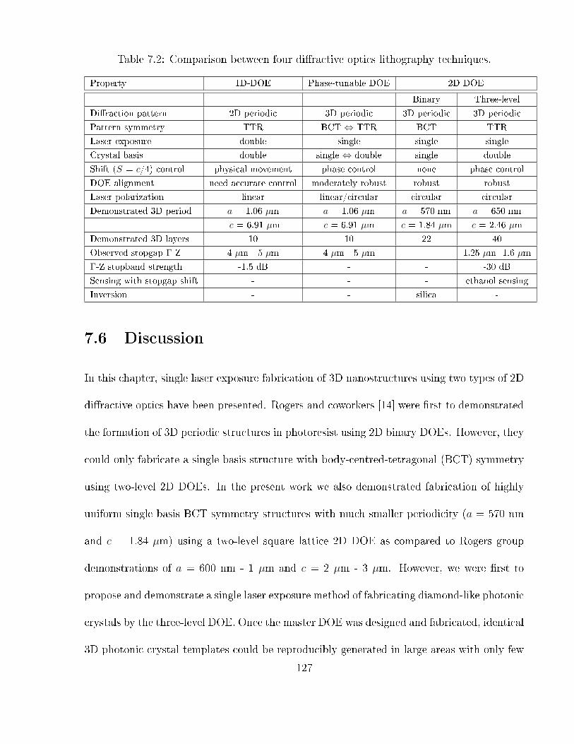
Table 7.2: Comparison between four di�ractive optics lithography techniques.
Property 1D-DOE Phase-tunable DOE 2D DOE
Binary Three-level
Di�raction pattern 2D periodic 3D periodic 3D periodic 3D periodic
Pattern symmetry TTR BCT ⇔ TTR BCT TTR
Laser exposure double single single single
Crystal basis double single ⇔ double single double
Shift (S = c/4) control physical movement phase control none phase control
DOE alignment need accurate control moderately robust robust robust
Laser polarization linear linear/circular circular circular
Demonstrated 3D period a = 1.06 µm a = 1.06 µm a = 570 nm a = 650 nm
c = 6.91 µm c = 6.91 µm c = 1.84 µm c = 2.46 µm
Demonstrated 3D layers 10 10 22 40
Observed stopgap Γ-Z 4 µm - 5 µm 4 µm - 5 µm - 1.25 µm -1.6 µm
Γ-Z stopband strength -1.5 dB - - -30 dB
Sensing with stopgap shift - - - ethanol sensing
Inversion - - silica -
7.6 Discussion
In this chapter, single laser exposure fabrication of 3D nanostructures using two types of 2D
di�ractive optics have been presented. Rogers and coworkers [14] were �rst to demonstrated
the formation of 3D periodic structures in photoresist using 2D binary DOEs. However, they
could only fabricate a single basis structure with body-centred-tetragonal (BCT) symmetry
using two-level 2D DOEs. In the present work we also demonstrated fabrication of highly
uniform single basis BCT symmetry structures with much smaller periodicity (a = 570 nm
and c = 1.84 µm) using a two-level square lattice 2D DOE as compared to Rogers group
demonstrations of a = 600 nm - 1 µm and c = 2 µm - 3 µm. However, we were �rst to
propose and demonstrate a single laser exposure method of fabricating diamond-like photonic
crystals by the three-level DOE. Once the master DOE was designed and fabricated, identical
3D photonic crystal templates could be reproducibly generated in large areas with only few
127

seconds of laser exposure. A short-period three-level DOE (Λ = 650 nm) was laser-fabricated
and applied to form 3D periodic structures in photoresist that con�rm formation of thick (>
40 layers), large area diamond-like nanostructures closely matching isointensity predictions
of �nite di�erence time domain computation. Spectroscopic characterization of the polymer
structure revealed a strong stopband along the Γ-Z direction in the telecom band that was
consistent with calculated band dispersion curves for the low-index medium. Due to its
porous 3D structure, such media are attractive in sensor applications where a complete
bandgap is not essential.
For cases where a wide complete photonic bandgap is desirable, such structures must be
inverted with a high refractive index material. However, a di�erent DOE design is required
that can further reduce the axial-to-transverse periodicity (c/a), for example, to c/a = 1.2
value for wide complete bandgap diamond-like woodpile structures as described in Section
4.3. Further optical engineering is therefore required to tune the present di�ractive optic
lithography method towards longer laser wavelength (λd), shorter period di�ractive structure
(Λ) and higher refractive index for the DOE grooves (nd) and background (nb) [36] according
to the generic design guidelines presented in Chapter 4.
128

Chapter 8
Applications of polymer 3D periodic
structures
8.1 Introduction
The present work has provided a wide range of 3D periodic nanostructures with uniform op-
tical and structural properties over large sample area (∼2-3 mm diameter) and through large
15-50 µm thickness with a large number of layers (> 40). The short exposure time and small
number of process steps shows promise for scaling to very large volume fabrication, dramat-
ically improving the throughput, quality and structural uniformity of 3D nanostructures,
especially over that provided by tedious and costly semiconductor processing technology.
Even a �exible fabrication approach like 3D laser direct write becomes unacceptably time
consuming when processing sample sizes of only 100 microns. In contrast, di�ractive optic
lithography approach is a parallel processing method that is easily scalable to generating
centimeter-scale 3D nanostructures having large number of layers in several seconds. We are
optimistic that the practical merits of this 3D fabrication technique will enable new practical
manufacturing methods for optical and MEMS applications of such 3D nanostructures.
129
8.2 Applications of polymer 3D photonic crystals
One of the applications we are investigating is embedding 3D photonic crystal structures into
micro-�uidic channels. This will serve two di�erent purposes. In one application, the em-
bedded 3D structures will enable chromatographic separation of cells using electro-�uorosis
and in the other application it will enable optical �uid sensing using stopgap information
of these structures. The ultimate goal is to combine these methods for optical detection of
biological and chemical species.
8.2.1 Fluid sensing with the shift in stopband
The usefulness of the strong stopbands reported for the woodpile structure shown in Fig.
7.5 has been tested by immersing the open crystal with ethanol while recording the optical
transmission spectrum. An 8 µL volume of ethanol (n = 1.34) was uniformly sprayed on a
5 mm x 5 mm sample surface area with a micro-pipette. Figure-8.1 shows the transmission
spectrum of the air-�lled stopband (t = 0-) and the stopband shifts at �rst immersion (t =
0+) and various times thereafter (2 to 24 min) as the solvent evaporates. The stopband nearly
disappears on �rst immersion, and then recovers by shifting from ∼1.26 µm wavelength back
to the original stopband (λ0 = 1.3 µm) after complete evaporation. The stopband shifting
speed can be controlled with the volume of ethanol used to �ll the open 3D crystal volume.
Contrary to simple Bragg considerations, the stopband shift to shorter wavelength in the
presence of ethanol is unexpected and may be due to anomalous dispersion of the higher order
stopbands (the stopband is between 5th and 6th band). Nevertheless, the open structure of
the present 3D diamond-like �lms o�er strong and narrow stopbands that are attractive
for optical sensing application. Such sensing structures can be integrated with cavities
130

Figure 8.1: Transmission recording of Γ-Z stopband of the woodpile structure shown inFig. 7.5 of Chapter 7 during Ethanol immersion (t = 0+ ) and evaporation (t > 0+) andcorresponding comparison with air-�lled photonic crystal spectrum (t = 0-).
and waveguides for new micro-sensing applications and would thus bene�t from the more
reproducible and higher volume 3D fabrication method introduced in this research work.
8.2.2 Integration with opto-�uidic channels
The 3D periodic nanostructures can be embedded inside opto �uidic channels using di�erent
laser fabrication techniques combining with conventional semiconductor and soft lithographic
techniques. However, a single laser exposure simultaneous fabrication of 3D structures as
well as micro-�uidic channels is more attractive from ease of fabrication and integration
purposes. We demonstrated a shadow masking technique to de�ne micro-�uidic channels
inside 3D structures fabricated by di�ractive optic lithography method. The photoresist
layer (nr) is exposed through a combination of di�ractive phase element (nd) and amplitude
mask (nAM) as shown in Fig. 8.2 where ni represent the index matching �uid and ns is the
substrate. The di�ractive phase element de�nes the 3D periodic structure and the amplitude
mask shown in Fig. 8.2b de�nes the open space (i.e. �uidic channels, reservoirs etc.) on the
131
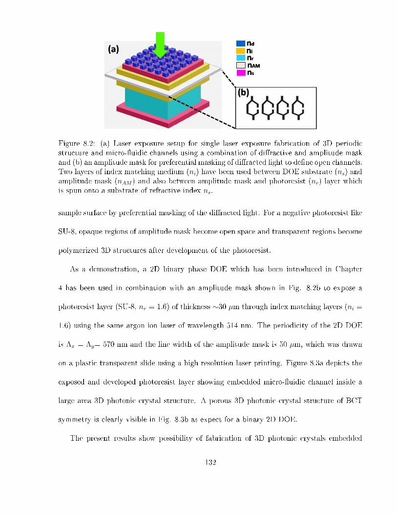
Figure 8.2: (a) Laser exposure setup for single laser exposure fabrication of 3D periodicstructure and micro-�uidic channels using a combination of di�ractive and amplitude maskand (b) an amplitude mask for preferential masking of di�racted light to de�ne open channels.Two layers of index matching medium (ni) have been used between DOE substrate (ns) andamplitude mask (nAM) and also between amplitude mask and photoresist (nr) layer whichis spun onto a substrate of refractive index ns.
sample surface by preferential masking of the di�racted light. For a negative photoresist like
SU-8, opaque regions of amplitude mask become open space and transparent regions become
polymerized 3D structures after development of the photoresist.
As a demonstration, a 2D binary phase DOE which has been introduced in Chapter
4 has been used in combination with an amplitude mask shown in Fig. 8.2b to expose a
photoresist layer (SU-8, nr = 1.6) of thickness ∼30 µm through index matching layers (ni =
1.6) using the same argon ion laser of wavelength 514 nm. The periodicity of the 2D DOE
is Λx = Λy= 570 nm and the line width of the amplitude mask is 50 µm, which was drawn
on a plastic transparent slide using a high resolution laser printing. Figure 8.3a depicts the
exposed and developed photoresist layer showing embedded micro-�uidic channel inside a
large area 3D photonic crystal structure. A porous 3D photonic crystal structure of BCT
symmetry is clearly visible in Fig. 8.3b as expect for a binary 2D DOE.
The present results show possibility of fabrication of 3D photonic crystals embedded
132
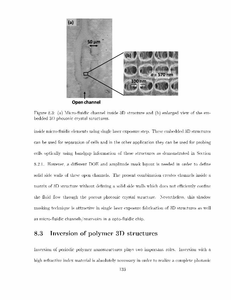
Figure 8.3: (a) Micro-�uidic channel inside 3D structure and (b) enlarged view of the em-bedded 3D photonic crystal structures.
inside micro-�uidic elements using single laser exposure step. These embedded 3D structures
can be used for separation of cells and in the other application they can be used for probing
cells optically using bandgap information of these structures as demonstrated in Section
8.2.1. However, a di�erent DOE and amplitude mask layout is needed in order to de�ne
solid side walls of these open channels. The present combination creates channels inside a
matrix of 3D structure without de�ning a solid side walls which does not e�ciently con�ne
the �uid �ow through the porous photonic crystal structure. Nevertheless, this shadow
masking technique is attractive in single laser exposure fabrication of 3D structures as well
as micro-�uidic channels/reservoirs in a opto-�uidic chip.
8.3 Inversion of polymer 3D structures
Inversion of periodic polymer nanostructures plays two important roles. Inversion with a
high refractive index material is absolutely necessary in order to realize a complete photonic
133
bandgap. The inversion process also highly bene�cial in converting a soft polymer structure
to a more durable robust structure. Ozin and co-workers has demonstrated that polymer
3D periodic structures can be inverted with silica (SiO2) using chemical vapor deposition
(CVD) technique [16]. Silica inversion is attractive in converting a �soft� SU-8 structure to a
�robust� structure made with a �hard� material. Silica is also attractive for bio-compatibility.
Moreover, silica inverted structures can be used as a �hard� template for silicon double
inversion using high temperature CVD [16] for complete bandgap device.
Due to large area uniformity of the single basis BCT symmetry structure produced by the
commercial two-level 2D-DOE of periodicity Λx = Λy= 570 nm (Section 7.3.1), this structure
was chosen for inversion. The 3D structure was fabricated in SU-8 photoresist using single
laser exposure of the 2D DOE and has been shown in Fig. 7.4.
8.3.1 Silica coating using chemical vapor deposition
The silica chemical vapor deposition has be performed in collaboration with my colleague
Nicole Zacharia in Geo�rey Ozin group. For the deposition of silica (SiO2) using CVD, the
polymer (SU-8) sample surfaces were �rst coated with a thin layer of water (H2O) by bubbling
nitrogen gas through water, and into the polymer sample. Next, using silicon tetrachloride
(SiCl4) as the precursor, silica was deposited on the sample surface. The chemical reaction
SiCl4+ 2H2O → SiO2+ 4HCl only takes place at the sample surfaces which leads to the
layer-by-layer growth of dense, amorphous SiO2 on the sample surfaces while releasing HCl
as a byproduct. The process is automatically terminated when the water is consumed [62].
This sequence is repeated until the desired thickness of the silica layer is reached.
For silica coating of the polymer structure shown in Fig. 7.4, the N2 �ow of 300 sccm
134
was directed through a bubbler �lled with twice-distilled H2O for 7 min, leading to a water
layer on the polymer sample surfaces. Subsequently, the CVD chamber was �ushed with N2
for 5 min. Then, the N2 �ow was directed for 10 min through a bubbler containing SiCl4
(Sigma�Aldrich 13736, > 99 %), which led to the layer-by-layer growth of silica on polymer
sample surface as shown in Fig. 8.4a-b. The sequence was repeated 3 times here in order to
deposit a 100-120 nm thick silica shell around the polymer structure.
8.3.2 Reactive ion etching of silica over-layer
The inner SU-8 �mother� template was removed to create a pure silica structure. To facilitate
removal of the inner SU-8 structure, �rst the top surface of the SiO2 over-layer was removed
by RIE in an SF6 plasma (etch time = 20 min, SF6 gas pressure = 22 mTorr and gas �ow rate
= 40 sccm, RIE power = 70 W) (Trion Ltd., Phantom Etcher RIE-ICP system) to exposure
SU-8 structure for subsequent polymer etching step. Figure 8.4c-d shows SEM images of top
and cross-sectional view of the structure after the SiO2 over-layer removal step.
8.3.3 Polymer template removal using reactive ion etching
The SU-8 template can be removed either by reactive ion etching using O2 plasma or by high
temperature (∼450oC ) calcination of SU-8 [16]. We found high temperature calcination to
be a more aggressive process and responsible for frequent 3D structural collapse. Instead
the SU-8 template was removed by gentle pure O2 plasma etching (etch time = 3.5 hr, O2
gas pressure = 50 mTorr, O2 gas �ow rate = 60 sccm and RIE power = 15 W). Figure 8.4e-f
shows SEM images of cross-sectional views of the focused ion beam (FIB) milled structure.
The SiO2 shells arranged on BCT point lattice can be clearly observed as expected after
removal of the SU-8 template. The quality of the SiO2 inversion can be gauged from energy-
135

Figure 8.4: Top (a) and cross-sectional (b) SEM images of SiO2 coated BCT symmetrystructure. (c) and (d) corresponding top and cross-sectional views after SiO2 over-layerremoval. (e) FIB milled cross-section after removal of SU-8 template and the correspondingenlarged cross-sectional view is shown in (f). EDX spectra (g) and material composition (h)showing ∼90% presence of SiO2 in the inverted structure.
dispersive X-ray spectroscopy (EDX) data given in Fig. 8.4g-h, con�rming ∼90% (weight)
presence of SiO2.
8.3.4 Optical characterization of silica inverted structures
The c/a = 1.54/0.57 = 2.7 ratio of the present single basis BCT symmetry structure is still
large as well as the refractive index of the photoresist (nr = 1.6) is too small to create photonic
stopgaps of the polymer BCT symmetry structure. However, stopgaps are predicted for the
136

Figure 8.5: Normalized transmission spectrum measured as normal angle of incidencethrough the structure in Fig. 8.4e showing a strong (-28 dB) stopband at 1.296 µm.
SiO2 inverted structure shown in Fig. 8.4e along several crystallographic directions. The
sample shown in Fig. 8.4e was optically probed along the Γ-Z direction (c axis in Fig. 7.4c)
with a broad band source in the 1.25 µm to 1.65 µm spectral range, providing the normalized
transmission spectrum shown in Fig. 8.5. All spectral recordings were normalized against
a reference spectrum recorded through an identical substrate coated with an identical SiO2
coating of ∼30 µm thickness. At 1.296-µm wavelength, a strong -28 dB attenuation stopband
with narrow response of ∼10 nm (FWHM) is observed.
The strong and narrow stopband (∼10 nm) indicates that all 22 layers in Fig. 8.4e-f are
collectively acting as coherent planes indicating formation of a highly uniform silica inverted
3D structure throughout the thick structure (30 µm) and over large area (2 mm diameter),
which would otherwise be washed out by minor lattice distortions for such narrow high-order
bands.
137
8.4 Summary
In summary, it has been demonstrated that strong and narrow stopgaps of polymer 3D
photonic crystal structures fabricated by di�ractive optics lithography technique can be used
in optical sensing applications. These 3D structures have been integrated into micro-�uidic
channels using shadow masking of the di�raction pattern. The polymer structures have been
e�ectively inverted with silica using chemical vapor deposition technique to convert a �soft�
polymer structure to a �robust� structure made with a �hard� material. The high quality
silica inverted structure promises possible use in biological sensing applications as well as
possible silicon double inversion for fabricating silicon 3D photonic crystals.
138
Chapter 9
Conclusion and future work
In Section 9.1, the present work has been compared with other published results in litera-
ture. In Section 9.2, the signi�cant scienti�c and engineering contributions of this thesis are
discussed. The dissertation is concluded with a outline for future work in Section 9.4.
9.1 Comparison with other literature results
Rogers and coworkers were �rst to demonstrate formation of 3D periodic structures in pho-
toresist using binary 2D DOEs [14]. However, as pointed out in Section 4.4.3.4, a binary
2D-DOE produces a single basis BCT symmetry di�raction pattern. Hence, 3D structures re-
ported by Rogers group remain restricted to only single-basis BCT symmetry structures with
lateral period (a) reported to be between 600 nm and 1 µm [14,63,64]. In the present work,
we also demonstrated fabrication of highly uniform single basis BCT symmetry structures
with much smaller periodicity (a = b = 570 nm and c = 1.84 µm) using a two-level square
lattice 2D DOE. The soft polymer BCT symmetry structures were successfully inverted with
silica to realize robust 3D nanostructures in Section 8.3.
Lin et al. extended DOEs to the fabrication of 3D �Woodpile�-type photonic crystal tem-
plates in photoresist by double exposures of orthogonal 1D-DOEs [15]. In the present thesis,
139
the fabrication precision was improved and the �rst spectral characterization of woodpile
photonic crystal templates formed by double laser exposure method was made [43]. Re-
cently, Chen and co-workers demonstrated fabrication of orthorhombic 3D structure using
the same double exposures method but with 600 rotated 1D-DOEs to interlace two 2D
structures with 600 angle [65]. To overcome the inherently imprecise DOE alignment that
arises between two laser exposures, we were �rst to devise a single laser exposure 3D peri-
odic structure fabrication method by back-to-back mounting of two linear phasemasks with
crossed grating orientation. This de�ned a phase-tunable DOE that permitted the �rst sin-
gle exposure near-�eld lithography based fabrication of the diamond-like structure [35]. We
subsequently demonstrated use of circularly polarized light for the �rst time to balance the
di�raction order e�ciencies and improve the structural uniformity [55]. Although, the phase
tunable near-�eld DOE method is versatile, it requires accurate phase control for fabrication
of diamond-like structure.
John and co-workers proposed a phasemask design based on orthogonal placement of
linear phasemasks on opposite surfaces of a single DOE substrate [56]. This requires tedious
etching and deposition processes on opposite surfaces of a substrate as well as precise control
of separation between two 1D gratings. We presented for the �rst time a single-surface
multi-level DOE design with locked-in phase-shift optimized for formation of diamond-like
photonic crystal structure in a single laser exposure step [36]. Rather than rely on the precise
control of substrate thickness [56], or the accurate physical separation of two DOEs for phase
control [35], a phase shift was built into the single-surface DOE design. This enabled ease of
etch of di�ractive elements on single side of a substrate. This new multi-level DOE design
permitted a large number of layers (> 40) to form in thick photoresist, generating a record
140

strength -30 dB stopband at 1.306 µm telecom band. The usefulness of this stopband for
refractive index sensing of liquids has been demonstrated.
9.2 Signi�cance of the present work
The present work demonstrated a simple 3D fabrication technique where once the master
DOE was designed and fabricated, identical 3D photonic crystal templates could be re-
producibly generated in large areas with only few seconds of laser exposure. Such DOE
fabrication is easily scalable to high volume and large area manufacturing of highly uniform
3D photonic crystals. The biggest contribution of the present work is demonstration of novel
phase control mechanisms to control near-�eld di�raction pattern. The phase control per-
mitted the �rst single exposure near-�eld lithography based fabrication of the diamond-like
structure. The phase control further o�ered formation of a continuum of other 3D periodic
structures that were tunable from the double basis diamond-like structure to a single basis
structure having body-centered-tetragonal symmetry. The present work has provided 3D pe-
riodic nanostructures with uniform optical and structural properties over large sample area
(∼3-4 mm diameter) and through large 15-50 µm thickness with large number of layers (>
40) having period of 550 nm to 1 µm and feature sizes between 100 nm and 400 nm. Pho-
tographs of one such large area uniform 3D sample which was fabricated using phase-tunable
di�ractive optics method, are shown in Fig. 9.1. Figure 9.1a-d were taken with di�erent
viewing angles where four di�erent viewing angles manifested as four di�erent sample colors.
The top SEM view of the sample is shown in Fig. 9.1e.
The refractive index of the photoresist was too small to create a complete photonic
bandgap. However, the presence of stopgaps were demonstrated for the woodpile structure
141
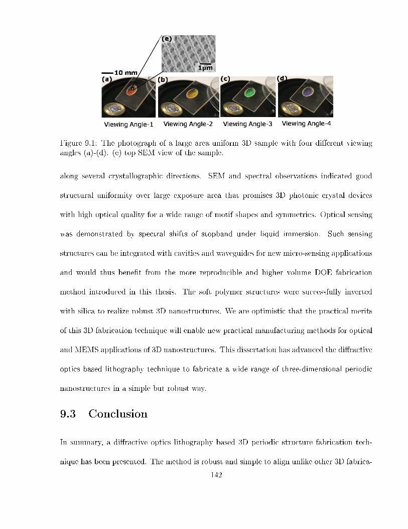
Figure 9.1: The photograph of a large area uniform 3D sample with four di�erent viewingangles (a)-(d). (e) top SEM view of the sample.
along several crystallographic directions. SEM and spectral observations indicated good
structural uniformity over large exposure area that promises 3D photonic crystal devices
with high optical quality for a wide range of motif shapes and symmetries. Optical sensing
was demonstrated by spectral shifts of stopband under liquid immersion. Such sensing
structures can be integrated with cavities and waveguides for new micro-sensing applications
and would thus bene�t from the more reproducible and higher volume DOE fabrication
method introduced in this thesis. The soft polymer structures were successfully inverted
with silica to realize robust 3D nanostructures. We are optimistic that the practical merits
of this 3D fabrication technique will enable new practical manufacturing methods for optical
and MEMS applications of 3D nanostructures. This dissertation has advanced the di�ractive
optics based lithography technique to fabricate a wide range of three-dimensional periodic
nanostructures in a simple but robust way.
9.3 Conclusion
In summary, a di�ractive optics lithography based 3D periodic structure fabrication tech-
nique has been presented. The method is robust and simple to align unlike other 3D fabrica-
142
tion techniques. The present work started with one-dimensional di�ractive optics for double
and single laser exposure fabrication of 3D periodic structures. However, imprecise align-
ment between two DOE exposures prevented double exposure method from reproducibly
generate 3D structures and a single exposure DOE method was therefore preferred for im-
proved uniformity and reproducibility. The phase-tunable DOE enabled DOE formation of
3D photonic crystal templates with a single laser exposure step. The controlled separation
of the two optical elements provided a variable phase shift to manipulate the interlacing
position of two orthogonally rotated periodic structures, and thereby facilitated fabrication
of diamond-like woodpile structures having tetragonal symmetry through to structures hav-
ing body-centered-tetragonal symmetry, and including variations in between. Although, the
phase tunable DOE method was versatile, it required accurate phase control in order to
provide a quarter period shift between two orthogonal interference patterns required for
diamond-like structure. To improve fabrication reproducibility of diamond-like structure,
a single-surface specially designed three-level DOE was proposed with locked-in phase-shift
optimized for formation of diamond-like photonic crystal structure in a single laser exposure
step. The three-level single-surface DOE was laser fabricated on a thin polymer �lm by
two-photon polymerization. Diamond-like structures were fabricated in photoresist having
Γ-Z (normal incidence) stopbands now shifted into the 1.25-1.65 µm telecom band [36] from
previous observations in the 3 to 5 µm range [43]. This new DOE design permitted a large
number of layers (> 40) to form in thick photoresist, generating a record strength -30 dB
stopband at 1.306 µm. The usefulness of this stopband for refractive index sensing of liquids
has been demonstrated. The soft polymer structures were successfully inverted with silica
to realize robust 3D nanostructures. The high quality silica inverted structure promises
143
possible use in biological sensing applications as well as possible silicon double inversion for
fabricating silicon 3D photonic crystals.
Three-dimensional periodic structure were consistently fabricated over large sample area
(∼2 mm diameter) and through large 10 - 30 µm thickness. The rapid exposure time (∼
5-10 s) and small number of process steps shows promise for scaling to very large volume
fabrication, dramatically improving the throughput, quality and structural uniformity of 3D
nanostructures, especially over that provided by tedious and costly semiconductor processing
technology. Even a �exible fabrication approach like 3D laser direct write becomes unac-
ceptably time consuming when processing sample sizes of only 100 microns. In contrast,
di�ractive optics lithography is a parallel processing method that is easily scalable to gener-
ating centimeter-scale 3D photonic crystals in several seconds when using high power lasers
and beam scanning exposure techniques.
9.4 Future directions
During this research work many scienti�c and technical di�culties have been encountered
and many of them systematically solved. However, quite a few technical directions remained
to be explored as listed below as future research directions.
1. Woodpile structure with complete bandgap
A polymer woodpile template fabricated according to the design guidelines given in
Section 4.3 will demonstrate a complete bandgap after inversion with a high refractive
index material. The complete bandgap is necessary in order to manipulate photons
to fabricate interesting optical devices like �lters, lasers, resonators, splitters. The
144

complete bandgap is also necessary for highly functional integrated photonic chips and
for the application of photonic bandgap properties to optical quantum information
processing. In the di�ractive optics method, the �rst step will be to fabricate a multi-
level DOE using high refractive index materials. Then the fabricated polymer structure
can be inverted with a high refractive index material like silicon. The process steps to
fabricate a woodpile structure with complete bandgap are listed below:
� Three-level DOE fabrication according to the design guidelines given in Section
4.3 using high refractive index materials.
� Suitable exposure laser to de�ne lattice constants (a and c) of the woodpile struc-
ture so that bandgap location can be tuned to a desired range. For example, if
the exposure laser wavelength is λd = 514 nm, the maximum bandgap condition
λd/Λ = 1.57 will create complete bandgap centred around λ = 650 nm. A longer
wavelength exposure laser is needed for a bandgap in the telecom band.
� The polymer 3D template can be inverted with silica according to the process
steps given in Section 8.3. Silica inversion is attractive in converting a �soft�
polymer structure to a �robust� structure made with a �hard� material. The silica
inverted structures can then be used as a �hard� template for silicon (double)
inversion using chemical vapor deposition technique [16].
2. Defect creation inside 3D periodic structures
For functionalization of 3D periodic structures, an engineered �defect� may be incorpo-
rated inside a perfectly periodic structure. However, the Talbot e�ect always creates
145
a periodic di�raction pattern and hence, direct incorporation of defect seems impos-
sible in di�ractive optics lithography. One possible solution is combining direct laser
writing [66,67] with DOE exposure. First the photoresist must be exposed with direct
laser writing to de�ne a defect and subsequently the same photoresist layer must be ex-
posed through a DOE to de�ne a 3D periodic structure. However, accurate alignment
is needed in order to register the defect in a precise location within the 3D periodic
pattern.
3. Integration of 3D nanostructures with micro-�uidic chips
The embedded 3D structures can be used for separation of cellular contents and in
the other application they can be used for probing cells optically using bandgap infor-
mation of these structures. The present results in Section 8.2.2 showed possibility of
fabrication of 3D photonic crystals embedded inside micro-�uidic elements using single
laser exposure step. However, a di�erent DOE and amplitude mask layout is needed in
order to de�ne solid side walls of these open channels. The present combination created
channels inside a matrix of 3D structure without de�ning a solid side wall which does
not e�ciently con�ne the �uid �ow through the porous photonic crystal structure.
146

Appendix A
Appendix-Derivation of Talbot length
from interference equations
The physical origin of Talbot self-images in the near-�eld or Fresnel region is the result
of addition of all di�raction orders with their phase delay di�erences equal to or integer
multiple of 2π [68, 69]. Figure- A.1 shows ray-optics picture of interference of di�erent
di�racted beams of a normally illuminated grating inside a medium of refractive index (nr)
placed in the Fresnel or near-�eld of the grating. The complete derivation of Talbot length
from interference equations assuming that only the three central di�raction orders (m =
-1, 0, 1) are propagating waves, i. e., 1 < Λ/λm ≤ 2, has been given below. Propagation
constants inside the medium are given in Eq. (A.1).
K0 =2πnrλd
[0 0 1] , K1 =2πnrλd
[sin θr 0 cos θr] , K−1 =2πnrλd
[− sin θr 0 cos θr] (A.1)
where λd is the free space wavelength, nr is the refractive index of the medium and θr is the
�rst order beam di�raction angle inside the medium. The di�raction angle θr can be related
to laser wavelength (λd) and grating period (Λ) by snell's law and law of di�raction as
sin θr =ninr
sin θi =ninr
λdniΛ
=λdnrΛ
(A.2)
The Talbot self-imaging condition is:
147
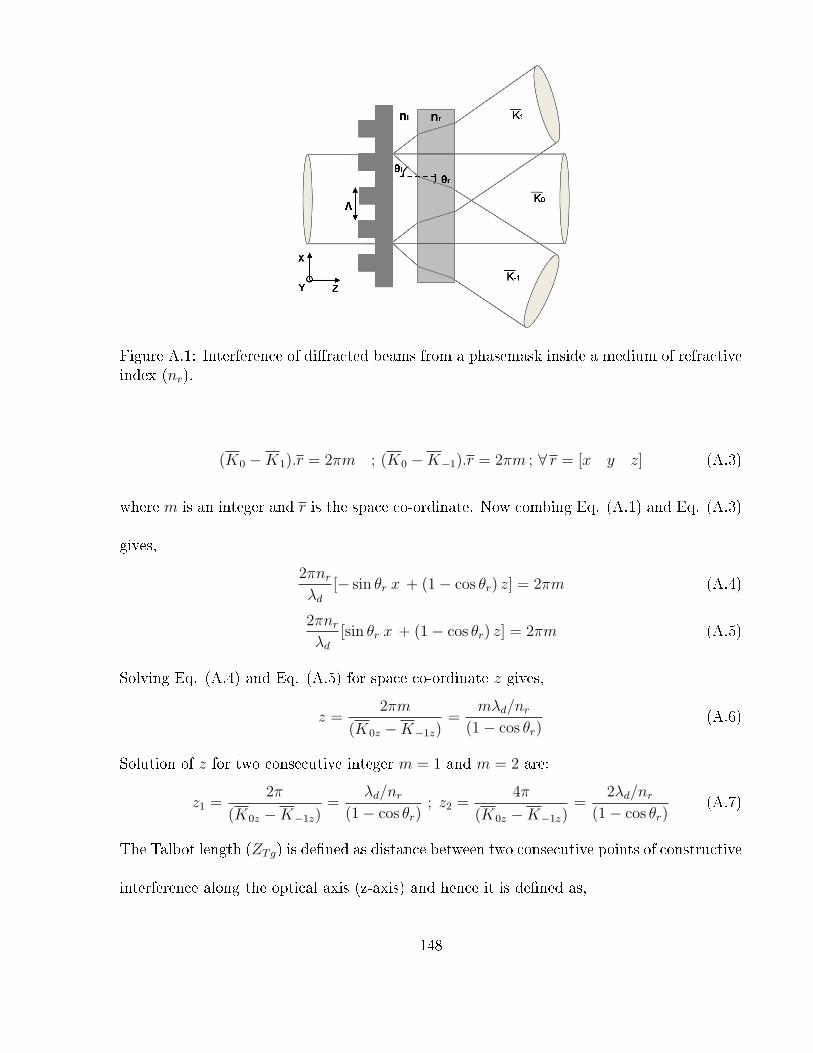
Figure A.1: Interference of di�racted beams from a phasemask inside a medium of refractiveindex (nr).
(K0 −K1).r = 2πm ; (K0 −K−1).r = 2πm ; ∀ r = [x y z] (A.3)
where m is an integer and r is the space co-ordinate. Now combing Eq. (A.1) and Eq. (A.3)
gives,
2πnrλd
[− sin θr x + (1− cos θr) z] = 2πm (A.4)
2πnrλd
[sin θr x + (1− cos θr) z] = 2πm (A.5)
Solving Eq. (A.4) and Eq. (A.5) for space co-ordinate z gives,
z =2πm
(K0z −K−1z)=
mλd/nr(1− cos θr)
(A.6)
Solution of z for two consecutive integer m = 1 and m = 2 are:
z1 =2π
(K0z −K−1z)=
λd/nr(1− cos θr)
; z2 =4π
(K0z −K−1z)=
2λd/nr(1− cos θr)
(A.7)
The Talbot length (ZTg) is de�ned as distance between two consecutive points of constructive
interference along the optical axis (z-axis) and hence it is de�ned as,
148

ZTg = (z2 − z1) =2π
(K0z −K−1z)=
λd/nr(1− cos θr)
=λd/nr
(1−√
[1− sin2 θr](A.8)
Now replacing Eq. (A.2) into Eq. (A.8) we get the �nal expression for generalized Talbot
length (ZTg) as given in Eq. (A.9).
ZTg =λd/nr
1−√
[1− ( λd
nrΛ)2]
(A.9)
149

Appendix B
Appendix-Photoresist sample
preparation
B.1 Recipe for photoresist sample preparation
Preparing good quality photoresist samples is extremely critical in producing high quality 3D
structures in a reproducible manner. During this research work a recipe has been developed
for SU-8 sample preparation for high quality 3D structure fabrication using CW laser at λ0
= 514 nm wavelength.
B.1.1 Chemicals required
The chemicals required for sample preparation are listed below:
� SU-8-2050 (From MicroChem)
� Purpose: photosensitive material.
� H-NU 470 (From Spectra group limited): Typical range 0.1% - 0.5% weight of SU-8.
For relatively low power exposure higher H-NU 470 concentration (0.4%-0.5% weight
of SU-8) is required to avoid long exposure time. H-NU 470 should be kept in a dry
moisture free place.
150
� Purpose: Photo initiator to increase photosensitivity of SU-8 at 514 nm. Since
SU-8 is optimized for i-line exposure (∼365 nm), photo-initiator is needed to
improve SU-8 absorption at 514 nm.
� TEA (Thriethylamine) (From ACP, Montreal): Typical range 0.2-0.3 molar ratio of
H-NU weight. For high resolution 3D fabrication (TEA: H-NU) mol ratio of (0.3:1) is
used which is equal to TEA amount = 7.99 µL for 0.5% of H-NU 470 concentration
considering molar weight of TEA = 101.1g/mol, molar weight of H-NU 470 = 520g/mol
and density of TEA = 0.73g/ml.
� Purpose: Reduces photosensitivity to background light for fabrication of porous
3D structures. However, use of TEA is optional. Details of use of TEA can be
found in Ref. [70].
� OPPI (From Spectra group limited): 2.5% weight of SU-8. OPPI has a shelve life of
maximum 6 months and should be kept in a dry moisture free place.
� Purpose: Photo co-initiator works in conjunction with H-NU 470.
� DMMA (N, N-dimethylacryl-amide-99%) (From Aldrich): Need enough amount to
dissolve H-NU 470 and OPPI.
� Purpose: Solvent to dissolve H-NU 470 and OPPI.
� Omnicoat (from MicroChem) : 6-8 ml for 25-30 samples (enough to completely coat
the surface of the glass substrates).
� Purpose: Improve adhesion between photoresist layer and glass substrate.
151

B.1.2 Cutting and cleaning glass substrates
Regular microscope slides are cut into square shapes of 1 in x 1 in. Substrates are cleaned
with Piranha (a mixture of sulfuric acid (H2SO4) and hydrogen peroxide (H2O2)) to remove
organic substances, dart etc.
B.1.3 Photoresist mixture preparation
� Use opaque bottles as containers to prevent strong penetration of visible light.
� Weigh H-NU 470 using a digital balance on weighing paper. Transfer H-NU 470 to
the opaque bottle and add an adequate amount of DMMA such that the H-NU 470 is
submerged. Use magnetic stirring to dissolve H-NU 470 into DMMA for approximately
1 hr. Try to place chemicals in the center of the bottom not to leave them on the wall
by accident. Avoid fast stirring to minimize splashing of solution to the sides of the
bottle.
� (Optional) Add TEA to the H-NU 470 + DMMA solution using a micro pipette. Need
to ensure all of the TEA is added by touching the side of the container with the pipette
needle close to the solution surface.
� Add OPPI to the H-NU 470 + DMMA + TEA solution. Need to add some more
DMMA to submerge the OPPI. Stir the mixture for Approx. 1 hr until it becomes
homogeneous mixture.
� Add 25% of total SU-8 to the H-NU 470 + DMMA + TEA + OPPI mixture and stir
for 6-8 hrs till it becomes a homogeneous mixture. Add remaining 75% of SU-8 to
the mixture and stir for 24 hours or more as required till it becomes a transparent
152
homogeneous mixture. Place a drop of the formulated photoresist between glass slides
and view it vertically in a light source such as an overhead projector or �ashlight. The
presence of any undissolved orange particles is an indication of incomplete solubility.
B.1.4 Spin-coating and baking
A uniform layer of SU-8 is spin coated on glass substrate following steps below:
� Dry piranha cleaned glass substrates with N2 gas or dry air and bake them @ 200 deg
C for 2-3 in. Keep them inside new plastic containers.
� Spin Omnicoat using two steps spin cycles of 500 rpm for 5s with acceleration 108 rpm
/s2 and then 3000 rpm with acceleration 324 rpm /s2 for 30s. Bake substrate at 200°C
for 2 minutes.
� Spin a thick photoresist layer (∼30 micrometers) using spin cycles of 500 rpm for 5s
with acceleration 108 rpm /s2 and then 3000 rpm for 50s with acceleration 324 rpm /
s2. Bake the thick photoresist sample at 65°C for 3 minutes and then at 95°C for 10
minutes. Keep samples away from visible light.
It has been observed that photosensitivity of H-NU 470 added SU-8 deteriorates with time.
One week time span between sample preparation and laser exposure has been found to be
optimal for producing high quality reproducible 3D structures.
153

Bibliography
[1] A. L. Schawlow and C. H. Townes, �Infrared and optical masers,� Physical Review
Letters, vol. 112, no. 6, pp. 1940�1949, 1958.
[2] T. H. Maiman, �Stimulated optical radiation in ruby,� Nature, vol. 187, pp. 493�494,
1960.
[3] E. Yablonovitch, �Inhibited spontaneous emission in solid-state physics and electronics,�
Physical Review Letters, vol. 58, no. 20, pp. 2059�2062, 1987.
[4] S. John, �Strong localization of photons in certain disordered dielectric superlattices,�
Physical Review Letters, vol. 58, no. 23, pp. 2486�2489, 1987.
[5] M. Plihal and A. A. Maradudin, �Photonic band structure of two-dimensional systems:
The triangular lattice,� Phys. Rev. B, vol. 44, no. 16, pp. 8565�8571, 1991.
[6] S. L. McCall, P. M. Platzman, R. Dalichaouch, D. Smith, and S. Schultz, �Microwave
propagation in two-dimensional dielectric lattices,� Phys. Rev. Lett., vol. 67, no. 15,
pp. 2017�2020, 1991.
[7] S. Y. Lin, J. G. Fleming, D. L. Hetherington, B. K. Smith, R. Biswas, K. M. Ho, M. M.
Sigalas, W. Zubrzycki, S. R. Kurtz, and J. Bur, �A three-dimensional photonic crystal
operating at infrared wavelengths,� Nature, vol. 394, no. 6690, pp. 251�253, 1998.
[8] S. Noda, K. Tomoda, N. Yamamoto, and A. Chutinan, �Full three-dimensional photonic
bandgap crystals at near-infrared wavelengths,� Science, vol. 289, no. 5479, pp. 604�606,
2000.
[9] M. Deubel, G. Von Freymann, M. Wegener, S. Pereira, K. Busch, and C. M. Soukoulis,
�Direct laser writing of three-dimensional photonic-crystal templates for telecommuni-
cations,� Nature Materials, vol. 3, no. 7, pp. 444�447, 2004.
154
[10] V. Mizeikis, K. Seet, S. Juodkazis, and H. Misawa, �Three-dimensional woodpile pho-
tonic crystal templates for the infrared spectral range,� Optics Letters, vol. 29, no. 17,
pp. 2061�2063, 2004.
[11] K. Busch, G. von Freymann, S. Linden, S. F. Mingaleev, L. Tkeshelashvili, and
M. Wegener, �Periodic nanostructures for photonics,� Physics Reports-Review Section
of Physics Letters, vol. 444, no. 3-6, pp. 101�202, 2007.
[12] M. Campbell, D. N. Sharp, M. T. Harrison, R. G. Denning, and A. J. Turber�eld,
�Fabrication of photonic crystals for the visible spectrum by holographic lithography,�
Nature, vol. 404, no. 6773, pp. 53�56, 2000.
[13] H. F. Talbot, �Facts relating to optical science,� Phil. Mag., vol. 9, no. 4, pp. 401�407,
1836.
[14] S. Jeon, J. U. Park, R. Cirelli, S. Yang, C. E. Heitzman, P. V. Braun, P. J. A. Kenis,
and J. A. Rogers, �Fabricating complex three-dimensional nanostructures with high-
resolution conformable phase masks,� Proceedings of the National Academy of Sciences
of the United States of America, vol. 101, no. 34, pp. 12428�12433, 2004.
[15] Y. Lin, P. R. Herman, and K. Darmawikarta, �Design and holographic fabrication of
tetragonal and cubic photonic crystals with phase mask: toward the mass-production
of three-dimensional photonic crystals,� Applied Physics Letters, vol. 86, no. 7, 2005.
[16] N. Tetreault, G. von Freymann, M. Deubel, M. Hermatschweiler, F. Perez-Willard,
S. John, M. Wegener, and G. A. Ozin, �New route to three-dimensional photonic
bandgap materials: Silicon double inversion of polymer templates,� Advanced Mate-
rials, vol. 18, no. 4, pp. 457�460, 2006.
[17] L. Rayleigh, �On the maintenance of vibrations by forces of double frequency, and
on the propagation of waves through a medium endowed with a periodic structure,�
Philosophical Magazine, vol. 24, pp. 145�159, 1887.
[18] E. Yablonovitch and T. J. Gmitter, �Photonic band structure: The face-centered-cubic
case,� Physical Review Letters, vol. 63, no. 18, pp. 1950�1953, 1989.
[19] K. M. Ho, C. T. Chan, and C. M. Soukoulis, �Comment on 'theory of photon bands in
three-dimensional periodic dielectric structures,� Physical Review Letters, vol. 66, no. 3,
p. 393, 1991.
155

[20] K. M. Ho, C. T. Chan, and C. M. Soukoulis, �Existence of a photonic gap in periodic
dielectric structures,� Physical Review Letters, vol. 65, no. 25, pp. 3152�3155, 1990.
[21] E. Yablonovitch, T. J. Gmitter, and K. M. Leung, �Photonic band structure: The face-
centered-cubic case employing nonspherical atoms,� Phys. Rev. Lett., vol. 67, no. 17,
pp. 2295�2298, 1991.
[22] O. Toader and S. John. PhD thesis, University of Toronto, 2003.
[23] N. W. Ashcroft and N. D. Mermin, Solid State Physics. Harcourt Brace College Pub-
lishers, 1976.
[24] K. M. Ho, C. T. Chan, C. M. Soukoulis, R. Biswas, and M. Sigalas, �Photonic band-gaps
in 3-dimensions - new layer-by-layer periodic structures,� Solid State Communications,
vol. 89, no. 5, pp. 413�416, 1994.
[25] A. L. Ingram and A. R. Parker, �A review of the diversity and evolution of photonic
structures in butter�ies, incorporating the work of john huxley (the natural history
museum, london from 1961 to 1990),� Philosophical Transactions of the Royal Society
B-Biological Sciences, vol. 363, no. 1502, pp. 2465�2480, 2008.
[26] J. W. Galusha, L. R. Richey, J. S. Gardner, J. N. Cha, and M. H. Bartl, �Discovery of a
diamond-based photonic crystal structure in beetle scales,� Physical Review E, vol. 77,
no. 5, p. 4, 2008.
[27] A. Blanco, E. Chomski, S. Grabtchak, M. Ibisate, S. John, S. W. Leonard, C. Lopez,
F. Meseguer, H. Miguez, J. P. Mondia, G. A. Ozin, O. Toader, and H. M. van Driel,
�Large-scale synthesis of a silicon photonic crystal with a complete three-dimensional
bandgap near 1.5 micrometres,� Nature, vol. 405, no. 6785, pp. 437�440, 2000.
[28] Y. A. Vlasov, X. Z. Bo, J. C. Sturm, and D. J. Norris, �On-chip natural assembly of
silicon photonic bandgap crystals,� Nature, vol. 414, pp. 289�293, 2001.
[29] K. Busch and S. John, �Photonic band gap formation in certain self-organizing systems,�
Physical Review E, vol. 58, pp. 3896�3908, 1998.
[30] M. Hermatschweiler, A. Ledermann, G. A. Ozin, M. Wegener, and G. von Freymann,
�Fabrication of silicon inverse woodpile photonic crystals,� Advanced Functional Mate-
rials, vol. 17, no. 14, pp. 2273�2277, 2007.
156
[31] J. S. King, E. Graugnard, O. M. Roche, D. N. Sharp, J. Scrimgeour, R. G. Denning, A. J.
Turber�eld, and C. J. Summers, �In�ltration and inversion of holographically de�ned
polymer photonic crystal templates by atomic layer deposition,� Advanced Materials,
vol. 18, no. 12, pp. 1561�1565, 2006.
[32] S. Shoji and S. Kawata, �Photofabrication of three-dimensional photonic crystals by
multibeam laser interference into a photopolymerizable resin,� Applied Physics Letters,
vol. 76, no. 19, pp. 2668�2670, 2000.
[33] Y. V. Miklyaev, D. C. Meisel, A. Blanco, G. von Freymann, K. Busch, W. Koch,
C. Enkrich, M. Deubel, and M. Wegener, �Three-dimensional face-centered-cubic pho-
tonic crystal templates by laser holography: fabrication, optical characterization, and
band-structure calculations,� Appl. Phys. Lett., vol. 82, no. 8, pp. 1284�1286, 2003.
[34] X. Wang, J. F. Xu, H. M. Su, Z. H. Zeng, Y. L. Chen, H. Z. Wang, Y. K. Pang, and
W. Y. Tam, �Three-dimensional photonic crystals fabricated by visible light holographic
lithography,� Appl. Phys. Lett., vol. 82, no. 14, pp. 2212�2214, 2003.
[35] D. Chanda and P. R. Herman, �Phase tunable multilevel di�ractive optical element
based single laser exposure fabrication of three-dimensional photonic crystal templates,�
Applied Physics Letters, vol. 91, no. 6, pp. 061122�1 061122�3, 2007.
[36] D. Chanda, L. Abolghasemi, M. Haque, M. Ng, and P. R. Herman, �Multi-level
di�ractive optics for single laser exposure fabrication of telecom-band diamond-like 3-
dimensional photonic crystals,� Optics Express, vol. 16, no. 20, pp. 15402�15414, 2008.
[37] J. T. Winthrop and Worthing.Cr, �Theory of fresnel images .i. plane periodis objects
in monochromatic light,� Journal of the Optical Society of America, vol. 55, no. 4,
pp. 373�381, 1965.
[38] E. Noponen and J. Turunen, �Electromagnetic theory of talbot imaging,� Optics Com-
munications, vol. 98, no. 1-3, pp. 132�140, 1993.
[39] A. W. Lohmann and J. A. Thomas, �Making an array illuminator based on the talbot
e�ect,� Applied Optics, vol. 29, no. 29, pp. 4337�4340, 1990.
[40] K. Patorski, Progress in Optics, vol. 27. Wolf, E., Amsterdam, North-Holland, 1989.
[41] D. C. O'Shea, T. J. Suleski, A. D. Kathman, and D. W. Prather, Di�ractive optics :
design, fabrication, and test. SPIE Publications, 2003.
157

[42] M. G. Moharam and T. K. Gaylord, �Rigorous coupled-wave analysis of planar-grating
di�raction,� J. Opt. Soc. Am., vol. 71, no. 7, pp. 811�818, 1981.
[43] D. Chanda, L. Abolghasemi, and P. R. Herman, �One-dimensional di�ractive optical
element based fabrication and spectral characterization of three-dimensional photonic
crystal templates,� Optics Express, vol. 14, no. 19, pp. 8568�8577, 2006.
[44] J. W. Goodman, Introduction to Fourier Optics. Roberts and Company, third ed., 2005.
[45] T. Kondo, S. Matsuo, S. Juodkazis, and H. Misawa, �Femtosecond laser interference
technique with di�ractive beam splitter for fabrication of three-dimensional photonic
crystals,� Applied Physics Letters, vol. 79, no. 6, pp. 725�727, 2001.
[46] J. H. Klein-Wiele and P. Simon, �Fabrication of periodic nanostructures by phase-
controlled multiple-beam interference,� Applied Physics Letters, vol. 83, no. 23,
pp. 4707�4709, 2003.
[47] R. Meade, A. Rappe, K. Brommer, J. Joannopoulos, and O. Alerhand, �Accurate theo-
retical analysis of photonic band-gap materials,� Phys. Rev. B, vol. 48, p. 8434, 1993.
[48] P. R. Villeneuve and M. Piche, �Photonic bandgaps in periodic dielectric structures,�
Progress in quantum electronics, vol. 18, pp. 153�200, 1994.
[49] D. Chanda, L. Abolghasemi, and P. R. Herman, �Numerical band calculation of holo-
graphically formed periodic structures with irregular motif,� in Photonics West (A. S.
Ali Adibi, Shawn-Yu Lin, ed.), vol. 6128 of Photonic Crystal Materials and Devices IV,
(San Jose, USA), pp. 311�316, SPIE, 2006.
[50] A. Chutinan and S. Noda. PhD thesis, Kyoto University, 2000.
[51] K. Leung and Y. Liu, �Full vector calculation of photonic band structures in face-
centered-cubic dielectric media,� Physical Review Letters, vol. 65, pp. 2646�2649, 1990.
[52] C. T. Chan, S. Datta, K. M. Ho, and C. M. Soukoulis, �A7 structure a family of photonic
crystals,� Physical Review B, vol. 50, no. 3, pp. 1988�1991, 1994.
[53] D. Chanda, L. Abolghasemi, and P. R. Herman, �Di�ractive optical elements based
fabrication of photonic crystals,� in Conference on Lasers and Electro-Optics (CLEO),
(Long Beach, USA), p. CMV7, OSA, 2006.
[54] J. Guild, The Interference Systems of Crossed Di�raction Gratings. Clarendon, Oxford,
1956.
158

[55] D. Chanda, L. E. Abolghasemi, and P. R. Herman, �Single laser exposure fabrication of
diamond-like 3-dimensional photonic crystal microstructure using circularly polarized
light,� Applied Physics A, vol. 93, pp. 33�37, 2008.
[56] T. Y. M. Chan, O. Toader, and S. John, �Photonic band-gap formation by optical-
phase-mask lithography,� Physical Review E, vol. 73, no. 4, p. 046610, 2006. Part 2.
[57] J. H. Jang, C. K. Ullal, M. Maldovan, T. Gorishnyy, S. Kooi, C. Y. Koh, and E. L.
Thomas, �3d micro- and nanostructures via interference lithography,� Advanced Func-
tional Materials, vol. 17, no. 16, pp. 3027�3041, 2007.
[58] D. Chanda and P. R. Herman, �Di�ractive optical elements based single-step fabrication
of 3-dimensional photonic crystal templates,� in Conference on Lasers and Electro-
Optics, (Baltimore, USA), p. CThW4, OSA, 2007.
[59] R. C. Rumpf and E. G. Johnson, �Fully three-dimensional modeling of the fabrication
and behavior of photonic crystals formed by holographic lithography,� Journal of the
Optical Society of America a-Optics Image Science and Vision, vol. 21, no. 9, pp. 1703�
1713, 2004.
[60] D. Chanda, L. Abolghasemi, and P. R. Herman, �Di�ractive optic near-�eld interference
based fabrication of telecom band diamond-like 3-dimensional photonic crystals,� in
Conference on Lasers and Electro-Optics, (San Jose, USA), p. CWO2, OSA, 2008.
[61] J. Serbin, A. Ovsianikov, and B. Chichkov, �Fabrication of woodpile structures by two-
photon polymerization and investigation of their optical properties,� Optics Express,
vol. 12, no. 21, pp. 5221�5228, 2004.
[62] H. Miguez, N. Tetreault, B. Hatton, S. Yang, D. Perovic, and G. A. Ozin, �Mechanical
stability enhancement by pore size and connectivity control in colloidal crystals by layer-
by-layer growth of oxide,� Chemical communications, vol. 22, no. 22, pp. 2736�2737,
2002.
[63] S. Jeon, V. Malyarchuk, J. A. Rogers, and G. P. Wiederrecht, �Fabricating three-
dimensional nanostructures using two photon lithography in a single exposure step,�
Optics Express, vol. 14, no. 6, pp. 2300�2308, 2006.
[64] D. J. Shir, S. Jeon, H. Liao, M. Highland, D. G. Cahill, M. F. Su, I. F. El-Kady, C. G.
Christodoulou, G. R. Bogart, A. V. Hamza, and J. A. Rogers, �Three-dimensional
nanofabrication with elastomeric phase masks,� Journal of Physical Chemistry B,
vol. 111, no. 45, pp. 12945�12958, 2007.
159

[65] Z. Poole, D. Xu, K. P. Chen, I. Olvera, K. Ohlinger, and Y. K. Lin, �Holographic
fabrication of three-dimensional orthorhombic and tetragonal photonic crystal templates
using a di�ractive optical element,� Applied Physics Letters, vol. 91, no. 25, p. 3, 2007.
[66] S. A. Rinne, F. Garcia-Santamaria, and P. V. Braun, �Embedded cavities and waveg-
uides in three-dimensional silicon photonic crystals,� Nature Photonics, vol. 2, no. 1,
pp. 52�56, 2008.
[67] C. H. Sun and P. Jiang, �Acclaimed defects,� Nature Photonics, vol. 2, no. 1, pp. 9�11,
2008.
[68] P. Latimer and R. F. Crouse, �Talbot e�ect reinterpreted,� Applied Optics, vol. 31, no. 1,
pp. 80�89, 1992.
[69] S. Teng, N. Zhang, Q. Dong, and C. Cheng, �Di�raction of a one-dimensional phase
grating in the deep fresnel �eld,� Journal of the Optical Society of America A-Optics
Image Science and Vision, vol. 24, no. 11, pp. 3636�3643, 2007.
[70] S. Yang, M. Megens, J. Aizenberg, P. Wiltzius, P. M. Chaikin, and W. B. Russel,
�Creating periodic three-dimensional structures by multibeam interference of visible
laser,� Chemistry of Materials, vol. 14, no. 7, pp. 2831�2833, 2002.
160


