187
Digital Compensation Schemes for Signal Distortion in OFDM Receivers July 2009 Mamiko Inamori
Digital Compensation Schemes for Signal
Distortion in OFDM Receivers
July 2009
Mamiko Inamori


Abstract
Various wireless standards have been developed for realizing broadband anywhere
/ anytime access network. Orthogonal division frequency multiplexing (OFDM)
is currently a dominant modulation scheme in broadband wireless systems. The
receiver is required to satisfy the conditions such as high-performance, low power
consumption, small size, and low cost. However, in the receiver for the broadband
signal, more accuracy of analog components is necessary and it leads to larger cost
and power consumption. To implement a low cost and low power consumption
receiver, compensation of the signal distortion in a digital domain is required. The
signal distortion compensation in the digital domain brings more scalability and
flexibility. In this dissertation, digital signal compensation schemes for the signal
distortion due to radio frequency (RF) components, timing jitter, and baseband
filter in OFDM receivers are proposed and investigated.
Chapter 1 introduces the background of the OFDM receivers and the motivation
of the research.
In Chapter 2, compensation schemes for signal distortion in a direct conversion
receiver are investigated. The OFDM direct conversion receiver is superior to a
superheterodyne receiver in cost, size, and power consumption. However, this
receiver architecture suffers from DC offset, frequency offset, and IQ imbalance.
In the proposed scheme, the key idea is to use a differential filter for the reduction
of the DC offset. From the outputs of differential filter in the training sequence,
the frequency offset is estimated with auto-correlation in the presence of DC offset.
The proposed scheme shows better estimation accuracy of the frequency offset than
the conventional scheme with a high pass filter. The IQ imbalance is calculated in
time domain using a simple equation without the impulse response of a channel
in the presence of the frequency offset and the DC offset. However, the accuracy
of the IQ imbalance estimation with the proposed scheme in the time domain
is deteriorated when the frequency offset is small. To overcome this problem,
frequency domain IQ imbalance estimation scheme is also proposed, which uses the
pilot subcarriers in the data period. Numerical results obtained through computer
iii

simulation show that estimation accuracy and bit error rate (BER) performance
can be improved even if the frequency offset is small. Thus, the combination of
two low-complexity IQ imbalance estimation schemes is suitable for low-cost and
low-power-consumption direct conversion receivers.
In Chapter 3, signal distortion caused by timing jitter is discussed. As one
of new receiver architectures, a RF-sampling receiver has been proposed, which
directly processes analog discrete samples. In this architecture, a phase locked
loop (PLL) exhibits the phase noise and then causes the timing jitter. In wireless
receivers, quadrature sampling is required in order to demodulate I-phase and Q-
phase signals. Different from simple charge sampling, timing jitter causes crosstalk
between these signals. In Chapter 3, the effect of the timing jitter on quadrature
sampling in the RF-sampling receiver is analyzed.
In Chapter 4, compensation schemes for signal distortion in fractional sampling
(FS) OFDM receivers are evaluated. The OFDM system with FS can achieve
diversity with a single antenna. However, as the number of subcarriers and the
oversampling ratio increase, the correlation among the noise components over dif-
ferent subcarriers deteriorates the BER performance. First, a correlated noise
cancellation scheme in FS orthogonal frequency and code division multiplexing
(OFCDM) system is investigated. To reduce the correlated noise, an alternative
spreading code (ASC) is used in the FS OFCDM system. This spreading code has
positive and negative components alternatively. Despreading with the ASC can-
cels most of the correlated noise components. However, this alternative spreading
code reduces the number of available spreading codes. For applicability to OFDM
systems, the effect of the correlation among the noise components in FS OFDM
system is derived. A metric weighting scheme for the coded FS OFDM system is
also proposed and investigated.
Chapter 5 summarizes the results of each chapter and concludes this disserta-
tion.
iv

Contents
Abstract iii
List of Acronyms xix
List of Notations xxiii
1 General Introduction 3
1.1 Broadband Wireless System . . . . . . . . . . . . . . . . . . . . . . 3
1.1.1 Broadband Cellular System . . . . . . . . . . . . . . . . . . 3
1.1.2 Broadband Wireless Access Network . . . . . . . . . . . . . 5
1.1.2.1 WPAN . . . . . . . . . . . . . . . . . . . . . . . . 6
1.1.2.2 WLAN . . . . . . . . . . . . . . . . . . . . . . . . 7
1.1.2.3 WMAN . . . . . . . . . . . . . . . . . . . . . . . . 8
1.1.2.4 WWAN . . . . . . . . . . . . . . . . . . . . . . . . 8
1.2 OFDM Receiver . . . . . . . . . . . . . . . . . . . . . . . . . . . . . 8
1.3 OFDM Receiver Architecture . . . . . . . . . . . . . . . . . . . . . 10
1.3.1 Superheterodyne Receiver . . . . . . . . . . . . . . . . . . . 10
1.3.2 Direct Conversion Receiver . . . . . . . . . . . . . . . . . . . 11
1.3.3 RF-sampling Receiver . . . . . . . . . . . . . . . . . . . . . 13
1.3.4 Fractional Sampling . . . . . . . . . . . . . . . . . . . . . . 14
1.4 Signal Distortion in OFDM Receivers . . . . . . . . . . . . . . . . . 17
1.4.1 Distortion due to RF Components . . . . . . . . . . . . . . . 17
1.4.2 Distortion due to PLL . . . . . . . . . . . . . . . . . . . . . 19
1.4.3 Distortion due to Baseband Filter . . . . . . . . . . . . . . . 20
1.5 Motivation of this Research . . . . . . . . . . . . . . . . . . . . . . 24
1.6 References . . . . . . . . . . . . . . . . . . . . . . . . . . . . . . . . 29
2 Frequency Offset and IQ Imbalance Estimation Scheme in the
v

Presence of Time-varying DC offset for Direct Conversion Re-
ceivers 37
2.1 Frequency Offset Estimation Scheme in the Presence of Time-varying
DC Offset for Direct Conversion Receivers . . . . . . . . . . . . . . 38
2.1.1 Introduction . . . . . . . . . . . . . . . . . . . . . . . . . . . 38
2.1.2 System Model . . . . . . . . . . . . . . . . . . . . . . . . . . 40
2.1.2.1 Preamble Model . . . . . . . . . . . . . . . . . . . 40
2.1.2.2 Subcarrier Allocation . . . . . . . . . . . . . . . . . 41
2.1.2.3 RF Architecture and Automatic Gain Control . . . 41
2.1.3 Frequency Offset Estimation . . . . . . . . . . . . . . . . . . 42
2.1.3.1 Coarse Estimation and Fine Estimation . . . . . . 42
2.1.3.2 Conventional Scheme . . . . . . . . . . . . . . . . . 42
2.1.3.3 Proposed Scheme . . . . . . . . . . . . . . . . . . . 43
2.1.3.4 Time-varying DC Offset . . . . . . . . . . . . . . . 45
2.1.4 Numerical Results . . . . . . . . . . . . . . . . . . . . . . . 47
2.1.4.1 Simulation Conditions . . . . . . . . . . . . . . . . 47
2.1.4.2 MSE vs. Threshold Level Under Time-varying DC
Offset . . . . . . . . . . . . . . . . . . . . . . . . . 48
2.1.4.3 MSE of Frequency Estimation Under Time-varying
DC Offset . . . . . . . . . . . . . . . . . . . . . . . 50
2.1.4.4 MSE vs. Threshold Level Under Constant DC Offset 50
2.1.4.5 MSE under Various Received Signal Power . . . . . 52
2.1.5 Conclusions . . . . . . . . . . . . . . . . . . . . . . . . . . . 52
2.2 Performance Analysis of Frequency Offset Estimation in the Pres-
ence of IQ Imbalance for OFDM Direct Conversion Receivers with
Differential Filter . . . . . . . . . . . . . . . . . . . . . . . . . . . . 52
2.2.1 Introduction . . . . . . . . . . . . . . . . . . . . . . . . . . . 53
2.2.2 System Model . . . . . . . . . . . . . . . . . . . . . . . . . . 53
2.2.3 Analysis of Frequency Offset Estimation . . . . . . . . . . . 54
2.2.3.1 Frequency Offset Estimation with Differential Filter 54
2.2.3.2 MSE Performance . . . . . . . . . . . . . . . . . . 56
2.2.4 Numerical Results . . . . . . . . . . . . . . . . . . . . . . . 59
2.2.4.1 Simulation Conditions . . . . . . . . . . . . . . . . 59
2.2.4.2 MSE Performance of Frequency Offset Estimation
under IQ imbalance . . . . . . . . . . . . . . . . . 60
2.2.5 Conclusions . . . . . . . . . . . . . . . . . . . . . . . . . . . 62
vi

2.3 Time Domain IQ Imbalance Estimation Scheme in the Presence of
Frequency Offset and Time-varying DC Offset for Direct Conversion
Receivers . . . . . . . . . . . . . . . . . . . . . . . . . . . . . . . . . 63
2.3.1 Introduction . . . . . . . . . . . . . . . . . . . . . . . . . . . 63
2.3.2 System Model . . . . . . . . . . . . . . . . . . . . . . . . . . 64
2.3.3 Frequency Offset Estimation . . . . . . . . . . . . . . . . . . 66
2.3.3.1 Frequency Offset, DC Offset, and IQ Imbalance
Model . . . . . . . . . . . . . . . . . . . . . . . . . 66
2.3.3.2 Frequency Offset Estimation Using Differential Filter 67
2.3.4 IQ Imbalance Estimation . . . . . . . . . . . . . . . . . . . . 68
2.3.4.1 IQ Imbalance Estimation . . . . . . . . . . . . . . 68
2.3.4.2 IQ Imbalance Compensation . . . . . . . . . . . . . 70
2.3.5 Simulation Results . . . . . . . . . . . . . . . . . . . . . . . 71
2.3.5.1 Simulation Conditions . . . . . . . . . . . . . . . . 71
2.3.5.2 Normalized MSE Performance of Phase Mismatch
Estimation vs. Phase Mismatch . . . . . . . . . . . 72
2.3.5.3 Normalized MSE Performance of Phase Mismatch
Estimation vs. Frequency Offset . . . . . . . . . . 73
2.3.5.4 Normalized MSE Performance of Gain Mismatch
Estimation . . . . . . . . . . . . . . . . . . . . . . 74
2.3.5.5 BER Performance . . . . . . . . . . . . . . . . . . 74
2.3.6 Conclusions . . . . . . . . . . . . . . . . . . . . . . . . . . . 76
2.4 Frequency Domain IQ Imbalance Estimation Scheme in the Presence
of DC Offset and Frequency Offset . . . . . . . . . . . . . . . . . . 76
2.4.1 Introduction . . . . . . . . . . . . . . . . . . . . . . . . . . . 76
2.4.2 System Model . . . . . . . . . . . . . . . . . . . . . . . . . . 77
2.4.3 Frequency Offset Estimation Using Differential Filter . . . . 78
2.4.4 Proposed IQ Imbalance Estimation . . . . . . . . . . . . . . 79
2.4.4.1 Influence of Differential Filter . . . . . . . . . . . . 79
2.4.4.2 IQ Imbalance Estimation without Frequency Offset 79
2.4.4.3 IQ imbalance Estimation in the presence of Fre-
quency Offset . . . . . . . . . . . . . . . . . . . . . 81
2.4.5 Simulation Results . . . . . . . . . . . . . . . . . . . . . . . 83
2.4.5.1 Simulation Conditions . . . . . . . . . . . . . . . . 83
2.4.5.2 Normalized MSE Performance vs. Frequency Offset 83
2.4.5.3 Normalized MSE Performance vs. Gain Mismatch
and Phase Mismatch . . . . . . . . . . . . . . . . . 85
vii
2.4.5.4 BER Performance vs. Frequency Offset . . . . . . . 88
2.4.5.5 BER Performance vs. Eb/N0 . . . . . . . . . . . . 89
2.4.6 Conclusions . . . . . . . . . . . . . . . . . . . . . . . . . . . 90
2.5 Conclusions of Chapter 2 . . . . . . . . . . . . . . . . . . . . . . . . 90
2.6 References . . . . . . . . . . . . . . . . . . . . . . . . . . . . . . . . 90
3 Effect of Timing Jitter on Quadrature Charge Sampling 95
3.1 Introduction . . . . . . . . . . . . . . . . . . . . . . . . . . . . . . . 95
3.2 System Model . . . . . . . . . . . . . . . . . . . . . . . . . . . . . . 96
3.2.1 Receiver Architecture . . . . . . . . . . . . . . . . . . . . . . 96
3.2.2 Charge Sampling Circuit . . . . . . . . . . . . . . . . . . . . 97
3.2.3 PLL Model . . . . . . . . . . . . . . . . . . . . . . . . . . . 97
3.3 Numerical Analysis . . . . . . . . . . . . . . . . . . . . . . . . . . . 99
3.3.1 Single Carrier QAM . . . . . . . . . . . . . . . . . . . . . . 99
3.3.2 OFDM Modulation . . . . . . . . . . . . . . . . . . . . . . . 103
3.3.3 SNR and SINR . . . . . . . . . . . . . . . . . . . . . . . . . 103
3.3.4 Comparison of Charge Sampling and Voltage Sampling . . . 104
3.4 Numerical Results . . . . . . . . . . . . . . . . . . . . . . . . . . . . 105
3.4.1 Simulation Conditions . . . . . . . . . . . . . . . . . . . . . 105
3.4.2 SNR and SINR . . . . . . . . . . . . . . . . . . . . . . . . . 106
3.4.3 BER . . . . . . . . . . . . . . . . . . . . . . . . . . . . . . . 107
3.5 Conclusions of Chapter 3 . . . . . . . . . . . . . . . . . . . . . . . . 108
3.6 References . . . . . . . . . . . . . . . . . . . . . . . . . . . . . . . . 109
4 Correlated Noise Cancellation Scheme in Fractional Sampling OFDM
System 113
4.1 Fractional Sampling OFCDM with Alternative Spreading Code . . . 113
4.1.1 Introduction . . . . . . . . . . . . . . . . . . . . . . . . . . . 114
4.1.2 System Model . . . . . . . . . . . . . . . . . . . . . . . . . . 114
4.1.2.1 Transmitter Model . . . . . . . . . . . . . . . . . . 114
4.1.2.2 Receiver Structure with Fractional Sampling . . . . 115
4.1.3 Proposed Scheme . . . . . . . . . . . . . . . . . . . . . . . . 116
4.1.3.1 Despreading with Non-alternative Spreading Code 116
4.1.3.2 Despreading with Alternative Spreading Code . . . 118
4.1.4 Numerical Results . . . . . . . . . . . . . . . . . . . . . . . 118
4.1.4.1 Simulation Conditions . . . . . . . . . . . . . . . . 118
4.1.4.2 BER Improvement with Alternative Spreading Code119
4.1.4.3 Number of Subcarriers . . . . . . . . . . . . . . . . 120
viii

4.1.4.4 Spreading Factor Sf . . . . . . . . . . . . . . . . . 121
4.1.4.5 Spreading Code . . . . . . . . . . . . . . . . . . . . 123
4.1.5 Conclusions . . . . . . . . . . . . . . . . . . . . . . . . . . . 124
4.2 Effect of Pulse Shaping Filters on a Fractional Sampling OFDM
System with Subcarrier-Based Maximal Ratio Combining . . . . . . 124
4.2.1 Introduction . . . . . . . . . . . . . . . . . . . . . . . . . . . 127
4.2.2 Receiver Structure with Fractional Sampling . . . . . . . . . 128
4.2.3 Noise Correlation among Samples . . . . . . . . . . . . . . . 128
4.2.4 Numerical Results . . . . . . . . . . . . . . . . . . . . . . . 130
4.2.4.1 Simulation Conditions . . . . . . . . . . . . . . . . 130
4.2.4.2 Channel Models . . . . . . . . . . . . . . . . . . . 131
4.2.4.3 Pulse Shaping Filters . . . . . . . . . . . . . . . . . 133
4.2.4.4 Frequency Spectrum of the Filter and Frobenius
Norm of the Whitening Matrix . . . . . . . . . . . 134
4.2.4.5 Uncoded FS OFDM . . . . . . . . . . . . . . . . . 136
4.2.4.6 Coded FS OFDM . . . . . . . . . . . . . . . . . . . 143
4.2.5 Conclusions . . . . . . . . . . . . . . . . . . . . . . . . . . . 146
4.3 Conclusions of Chapter 4 . . . . . . . . . . . . . . . . . . . . . . . . 146
4.4 References . . . . . . . . . . . . . . . . . . . . . . . . . . . . . . . . 147
5 Overall Conclusions 149
5.1 Signal Compensation Schemes in OFDM Direct Conversion Receivers149
5.2 Signal Compensation Schemes in RF-sampling Receivers . . . . . . 150
5.3 Signal Compensation Schemes in FS OFDM Receivers . . . . . . . . 151
Acknowledgements 153
List of Achievements 155
ix


List of Figures
1.1 Wireless standard. . . . . . . . . . . . . . . . . . . . . . . . . . . . 5
1.2 IEEE 802 standard. . . . . . . . . . . . . . . . . . . . . . . . . . . . 7
1.3 OFDM transmitter architecture. . . . . . . . . . . . . . . . . . . . . 9
1.4 OFDM receiver architecture. . . . . . . . . . . . . . . . . . . . . . . 10
1.5 Evolution of receiver architectures. . . . . . . . . . . . . . . . . . . 10
1.6 Superheterodyne receiver architecture. . . . . . . . . . . . . . . . . 11
1.7 Downconversion in superheterodyne receiver. . . . . . . . . . . . . . 11
1.8 Direct conversion receiver architecture. . . . . . . . . . . . . . . . . 12
1.9 Downconversion in direct conversion receiver. . . . . . . . . . . . . 12
1.10 DC offset and frequency offset. . . . . . . . . . . . . . . . . . . . . . 13
1.11 IQ imbalance model. . . . . . . . . . . . . . . . . . . . . . . . . . . 14
1.12 RF sampling receiver architecture. . . . . . . . . . . . . . . . . . . . 15
1.13 Downconversion in RF sampling receiver. . . . . . . . . . . . . . . . 15
1.14 Influence of timing jitter. . . . . . . . . . . . . . . . . . . . . . . . . 16
1.15 Influence of timing jitter. . . . . . . . . . . . . . . . . . . . . . . . . 17
1.16 Fractional sampling receiver. . . . . . . . . . . . . . . . . . . . . . . 17
1.17 Fractional sampling in delay domain. . . . . . . . . . . . . . . . . . 18
1.18 Correlation between noise components. . . . . . . . . . . . . . . . . 24
1.19 Overall structure of this research. . . . . . . . . . . . . . . . . . . . 25
1.20 Relationship of this research. . . . . . . . . . . . . . . . . . . . . . . 26
1.21 Overall model about distortion due to RF components. . . . . . . . 29
1.22 Overall model about distortion due to PLL. . . . . . . . . . . . . . 30
1.23 Overall model about distortion due to baseband filters. . . . . . . . 30
2.1 OFDM direct conversion architecture. . . . . . . . . . . . . . . . . . 39
2.2 IEEE 802.11a/g burst structure. . . . . . . . . . . . . . . . . . . . . 40
2.3 Subcarriers allocation. . . . . . . . . . . . . . . . . . . . . . . . . . 40
2.4 Receiver architecture. . . . . . . . . . . . . . . . . . . . . . . . . . . 41
xi
2.5 Effect of DC offset in conventional scheme. . . . . . . . . . . . . . . 43
2.6 Overall system model. . . . . . . . . . . . . . . . . . . . . . . . . . 44
2.7 DC offset and the output of differential filter. . . . . . . . . . . . . 46
2.8 LO leakage. . . . . . . . . . . . . . . . . . . . . . . . . . . . . . . . 48
2.9 MSE vs. threshold level performance of frequency offset estimation
(cutoff freq.=1[kHz], Eb/N0=15[dB]). . . . . . . . . . . . . . . . . . 48
2.10 MSE vs. threshold level performance of frequency offset estimation
(cutoff freq.=10[kHz], Eb/N0=15[dB]). . . . . . . . . . . . . . . . . 49
2.11 MSE vs. threshold level performance of frequency offset estimation
(cutoff freq.=100[kHz], Eb/N0=15[dB]). . . . . . . . . . . . . . . . . 49
2.12 MSE performance of frequency offset estimation under time-varying
DC offset (coarse+fine, cutoff freq.=10[kHz]). . . . . . . . . . . . . 50
2.13 MSE performance of frequency offset estimation under constant DC
offset (coarse+fine, cutoff freq.=10[kHz]). . . . . . . . . . . . . . . . 51
2.14 MSE vs. received signal power (Eb/N0=15[dB], cutoff freq.=10[kHz]). 51
2.15 Receiver architecture. . . . . . . . . . . . . . . . . . . . . . . . . . . 54
2.16 Vectors representation of auto-correlation. . . . . . . . . . . . . . . 57
2.17 Cancelation in auto-correlation. . . . . . . . . . . . . . . . . . . . . 58
2.18 MSE vs. SNR (β=0.05, θ=5[degrees]). . . . . . . . . . . . . . . . . 60
2.19 MSE vs. normalized frequency offset (θ=5[degrees], β=0.05). . . . . 61
2.20 MSE vs. gain mismatch (normalized freq. offset=0.3, θ=5[degrees]). 62
2.21 MSE vs. phase mismatch (normalized freq. offset=0.3, β=0.05). . . 62
2.22 DC offset and the output of differential filter. . . . . . . . . . . . . 65
2.23 Receiver architecture. . . . . . . . . . . . . . . . . . . . . . . . . . . 66
2.24 Normalized MSE performance of phase mismatch estimation vs.
phase mismatch (β=0.05, normalized freq. offset = 0.3). . . . . . . 72
2.25 Normalized MSE performance of phase mismatch estimation vs. fre-
quency offset (β=0.05, θ= 5[degrees]). . . . . . . . . . . . . . . . . 73
2.26 Normalized MSE performance of gain mismatch estimation (θ=
5[degrees], normalized freq. offset=0.3). . . . . . . . . . . . . . . . . 74
2.27 BER performance with 1st order interpolation (normalized freq. off-
set=0.3, β=0.05, θ=5[degrees]). . . . . . . . . . . . . . . . . . . . . 75
2.28 Subcarrier frequency allocation. . . . . . . . . . . . . . . . . . . . . 77
2.29 Vector representation of pilot subcarriers with IQ imbalance. . . . . 80
2.30 Receiver architecture of proposed scheme. . . . . . . . . . . . . . . 82
2.31 Effect of ICI and frequency offset. . . . . . . . . . . . . . . . . . . . 83
xii

2.32 Normalized MSE performance of gain mismatch estimation (β=0.05,
θ=5[degrees]). . . . . . . . . . . . . . . . . . . . . . . . . . . . . . . 84
2.33 Normalized MSE performance of phase mismatch estimation (β=0.05,
θ=5[degrees]). . . . . . . . . . . . . . . . . . . . . . . . . . . . . . . 85
2.34 Real part of the second term of Eq. (2.80) (SNR = ∞, β=0.05,
θ=5[degrees]). . . . . . . . . . . . . . . . . . . . . . . . . . . . . . . 86
2.35 Imaginary part of the second term of Eq. (2.80) (SNR = ∞, β=0.05,
θ=5[degrees]). . . . . . . . . . . . . . . . . . . . . . . . . . . . . . . 86
2.36 Normalized MSE performance of gain mismatch estimation (α=0.001,
θ=5[degrees]). . . . . . . . . . . . . . . . . . . . . . . . . . . . . . . 87
2.37 Normalized MSE performance of phase mismatch estimation (α=0.001,
β=0.05). . . . . . . . . . . . . . . . . . . . . . . . . . . . . . . . . . 87
2.38 BER vs. normalized frequency offset α (64QAM, β=0.05, θ=5[degrees]). 88
2.39 BER vs. Eb/N0 (64QAM, β=0.05, θ=5[degrees]). . . . . . . . . . . 89
3.1 Block diagram of the receiver. . . . . . . . . . . . . . . . . . . . . . 97
3.2 Simple integrating charge sampling circuit. . . . . . . . . . . . . . . 97
3.3 Block diagram of the PLL. . . . . . . . . . . . . . . . . . . . . . . . 98
3.4 Typical PSD of the PLL phase noise. . . . . . . . . . . . . . . . . . 98
3.5 Modeled PSD of the PLL phase noise. . . . . . . . . . . . . . . . . 99
3.6 Quadrature sampling. . . . . . . . . . . . . . . . . . . . . . . . . . . 100
3.7 Sampling of the I-phase component. . . . . . . . . . . . . . . . . . . 101
3.8 SNR and SINR versus symbol rate, (single carrier, Eb/N0 = 14 [dB]).107
3.9 SNR and SINR versus symbol rate, (OFDM, Eb/N0 = 14 [dB]). . . 108
3.10 BER versus Eb/No, (Ng =-100 [dBc/Hz], symbol rate=100 [Msym-
bol/s], single carrier 64QAM). . . . . . . . . . . . . . . . . . . . . . 108
3.11 BER versus symbol rate (Ng = -100 [dBc/Hz], Eb/N0 = 14 [dB],
single carrier 64QAM). . . . . . . . . . . . . . . . . . . . . . . . . . 109
4.1 OFCDM transmitter block diagram. . . . . . . . . . . . . . . . . . . 115
4.2 Receiver block diagram. . . . . . . . . . . . . . . . . . . . . . . . . 115
4.3 Correlation of the noise components (logarithmic representation of
absolute value). . . . . . . . . . . . . . . . . . . . . . . . . . . . . . 116
4.4 PSD vs. normalized frequency with different pulse shapes. . . . . . 120
4.5 Multipath channel models. . . . . . . . . . . . . . . . . . . . . . . . 121
4.6 BER performance vs. Eb/N0 on the 16 path Rayleigh fading channel
with the uniform delay profile (number of subcarriers: 1024, Sf=2). 122
xiii

4.7 BER performance vs. Eb/N0 on the 24 path Rayleigh fading channel
with the exponential delay profile (number of subcarriers: 1024,
Sf=2). . . . . . . . . . . . . . . . . . . . . . . . . . . . . . . . . . . 123
4.8 BER performance vs. number of subcarriers on the 16 path Rayleigh
fading channel with the uniform delay profile (Sf = 2, Eb/N0 =
15[dB]). . . . . . . . . . . . . . . . . . . . . . . . . . . . . . . . . . 124
4.9 BER performance vs. number of subcarriers on the 24 path Rayleigh
fading channel with the exponential delay profile (Sf = 2, Eb/N0 =
15[dB]). . . . . . . . . . . . . . . . . . . . . . . . . . . . . . . . . . 125
4.10 BER performance vs. spreading factor Sf on the 16 path Rayleigh
fading channel with the uniform delay profile (number of subcarri-
ers:1024, Eb/N0 = 15[dB]). . . . . . . . . . . . . . . . . . . . . . . . 125
4.11 BER performance vs. spreading factor Sf on the 24 path Rayleigh
fading channel with the exponential delay profile (number of sub-
carriers:1024, Eb/N0 = 15[dB]). . . . . . . . . . . . . . . . . . . . . 126
4.12 BER performance vs. G with different spreading codes on the 16
path Rayleigh fading channel with the uniform delay profile (number
of subcarriers:1024, Eb/N0 = 15[dB]). . . . . . . . . . . . . . . . . . 126
4.13 BER performance vs. G with different spreading codes on the 24
path Rayleigh fading channel with the exponential delay profile
(number of subcarriers:1024, Eb/N0 = 15[dB]). . . . . . . . . . . . . 127
4.14 Block diagram of a receiver. . . . . . . . . . . . . . . . . . . . . . . 128
4.15 Correlation of the noise components (logarithm representation of
absolute value). . . . . . . . . . . . . . . . . . . . . . . . . . . . . . 129
4.16 6-ray GSM Typical Urban model. . . . . . . . . . . . . . . . . . . . 131
4.17 Multipath Rayleigh fading channel models. . . . . . . . . . . . . . 132
4.18 Graphical illustration of the pulse shaping filters. . . . . . . . . . . 133
4.19 Frobenius norm of the whitening filter for different impulse responses
(Number of subcarriers=64, G = 2). . . . . . . . . . . . . . . . . . 135
4.20 Frobenius norm of the whitening filter for different impulse responses
(Number of subcarriers=64, G = 4). . . . . . . . . . . . . . . . . . 135
4.21 Frobenius norm of the whitening filter for different impulse responses
(Number of subcarriers=1024, G = 4). . . . . . . . . . . . . . . . . 136
4.22 BER performance vs. Eb/N0 on the 16 path Rayleigh fading channel
with the uniform delay profile (QPSK, Number of subcarriers=64,
G = 1). . . . . . . . . . . . . . . . . . . . . . . . . . . . . . . . . . 137
xiv
4.23 BER performance vs. Eb/N0 on the 16 path Rayleigh fading channel
with the uniform delay profile (QPSK, Number of subcarriers=64,
G = 2). . . . . . . . . . . . . . . . . . . . . . . . . . . . . . . . . . 137
4.24 BER performance vs. Eb/N0 on the 16 path Rayleigh fading channel
with the uniform delay profile (QPSK, Number of subcarriers=64,
G = 4). . . . . . . . . . . . . . . . . . . . . . . . . . . . . . . . . . 138
4.25 BER performance vs. Eb/N0 on the 16 path Rayleigh fading channel
with the uniform delay profile (16QAM, Number of subcarriers=64,
G = 4). . . . . . . . . . . . . . . . . . . . . . . . . . . . . . . . . . 138
4.26 BER performance vs. Eb/N0 on the 16 path Rayleigh fading channel
with the uniform delay profile (64QAM, Number of subcarriers=64,
G = 4). . . . . . . . . . . . . . . . . . . . . . . . . . . . . . . . . . 139
4.27 BER performance vs. Eb/N0 on the 16 path Rayleigh fading channel
with the uniform delay profile (QPSK, Number of subcarriers=1024,
G = 4). . . . . . . . . . . . . . . . . . . . . . . . . . . . . . . . . . 140
4.28 BER performance vs. Eb/N0 on the 16 path Rayleigh fading chan-
nel with the uniform delay profile (16QAM, Number of subcarri-
ers=1024, G = 4). . . . . . . . . . . . . . . . . . . . . . . . . . . . . 140
4.29 BER performance vs. Eb/N0 on the 16 path Rayleigh fading chan-
nel with the uniform delay profile (64QAM, Number of subcarri-
ers=1024, G = 4). . . . . . . . . . . . . . . . . . . . . . . . . . . . . 141
4.30 BER performance vs. Eb/N0 on the 24 path Rayleigh fading chan-
nel with the exponential delay profile (QPSK, Number of subcarri-
ers=1024, G = 4). . . . . . . . . . . . . . . . . . . . . . . . . . . . . 141
4.31 BER performance vs. Eb/N0 on the GSM Typical Urban model
(QPSK, Number of subcarriers=1024,G = 4). . . . . . . . . . . . . 142
4.32 BER performance vs. Eb/N0 of coded OFDM (QPSK, Number of
subcarriers=64, G = 4). . . . . . . . . . . . . . . . . . . . . . . . . 144
4.33 BER performance vs. Eb/N0 of coded OFDM with Adjusted Metric
(QPSK, Number of subcarriers=64, G = 4). . . . . . . . . . . . . . 144
4.34 BER performance vs. Eb/N0 of coded OFDM (QPSK, Number of
subcarriers=1024, G = 4). . . . . . . . . . . . . . . . . . . . . . . . 145
4.35 BER performance vs. Eb/N0 of coded OFDM with Adjusted Metric
(QPSK, Number of subcarriers=1024, G = 4). . . . . . . . . . . . . 145
xv


List of Tables
1.1 Cellular systems. . . . . . . . . . . . . . . . . . . . . . . . . . . . . 6
1.2 IEEE 802.11 protocols. . . . . . . . . . . . . . . . . . . . . . . . . . 9
1.3 Outline of the proposed approaches. . . . . . . . . . . . . . . . . . . 31
2.1 Simulation conditions. . . . . . . . . . . . . . . . . . . . . . . . . . 47
2.2 Simulation conditions. . . . . . . . . . . . . . . . . . . . . . . . . . 60
2.3 Simulation conditions. . . . . . . . . . . . . . . . . . . . . . . . . . 71
2.4 Pilot subcarriers. . . . . . . . . . . . . . . . . . . . . . . . . . . . . 79
2.5 Simulation conditions. . . . . . . . . . . . . . . . . . . . . . . . . . 84
3.1 Simulation conditions. . . . . . . . . . . . . . . . . . . . . . . . . . 106
4.1 Simulation conditions. . . . . . . . . . . . . . . . . . . . . . . . . . 119
4.2 Spreading code. . . . . . . . . . . . . . . . . . . . . . . . . . . . . . 122
4.3 Simulation conditions . . . . . . . . . . . . . . . . . . . . . . . . . . 130
4.4 6-ray GSM Typical Urban model parameters. . . . . . . . . . . . . 131
xvii


List of Acronyms
1G first generation
2G second generation
3G third generation
3GPP third generation partnership project
3GPP2 third generation partnership project 2
3.9G 3.9 generation
4G fourth generation
64QAM quadrature amplitude modulation
A/D analog-to-digital
ADC analog-to-digital converter
AGC automatic gain control
AFC automatic frequency control
AWGN additive white Gaussian noise
BER bit error rate
BPF band pass filter
CDMA code division multiple access
CMOS complementary metal oxide semiconductor
DC direct current
DFT discrete Fourier transform
DS/SS direct sequence / spread-spectrum
FCC federal communications commission
FDMA frequency division multiple access
FIR finite impulse response
FS fractional sampling
GI guard interval
HPF high pass filter
HSDPA High Speed Downlink Packet Access
I in-phase
ICI intercarrier interference
IEEE institute of electrical and electronics engineers
IF intermediate frequency
xix

IDFT inverse discrete Fourier transform
IMT-2000 International Mobile Telecommunications-2000
IR-UWB impulse-radio UWB
ISI intersymbol interference
ISM industrial, scientific and medical
ITU international telecommunication union
LNA low noise amplifier
LO local oscillator
LPF low pass filter
LTE long term evolution
LTSP long training sequence preamble
MB-OFDM multiband-OFDM
MBWA mobile broadband wireless access
MIMO multiple-input multiple-output
MRC maximal ratio combing
MSE mean square error
OFCDM orthogonal frequency and code division multiplexing
OFDM orthogonal frequency division multiplexing
OFDMA orthogonal frequency division multiplexing access
PLL phase locked loop
P/S parallel-to-serial
PSD power spectrum density
Q quadrature
QOCRC quadrature overlapped cubed raised cosine
QOSRC Quadrature overlapped squared raised cosine
QoS quality of service
QPSK quadrature phase-shift keying
RF radio frequency
RSSI receive signal strength indicator
SAW surface acoustic wave
SIMO single-input multiple-output
SINR signal-to-interference and noise ratio
SISO single-input single-output channel
SNR signal-to-noise ratio
S/P serial-to-parallel
STSP short training sequence preamble
TCXO temperature-compensated crystal oscillator
TDMA time division multiple access
USB universal serial bus
UWB ultra-wide band
xx
VCO voltage-controlled oscillator
VGA variable gain amplifier
WCDMA Wideband-Code Division Multiple Access
WiMAX Worldwide Interoperability for Microwave Access
WLAN wireless local network
WMAN wireless metropolitan area network
WPAN wireless personal area network
WWAN wireless wide area network
xxi


List of Notations
a roll-off factor of root cosine roll-off filterAI amplitude of I-phase componentAQ amplitude of Q-phase componentAI [n] n-th sampled amplitude of I-phase componentAQ[n] n-th sampled amplitude of Q-phase componentc(t) impulse response of the physical channelCadd numbers of complex additionsCmult numbers of complex multiplicationsCdiv numbers of complex divisionsCε numbers of calculations to estimate ε
dSP [n] n-th STSP output signal after differential filteringdSP [n] n-th STSP output with IQ imbalance after the differential filterD[k] output after the differential filter in the frequency domainfB cutoff frequency of filterfc RF carrier frequencyfs symbol rateg oversampling indexG oversampling ratioh(t) impulse response of the composite channelhg[n] sampled h(t) at (nTs + gTs/G)HDF[k] channel response of the differential filterH[k] channel response of the k-th subcarrierH ′[k] H[k] after noise whiteningHg[k] frequency response of hg[n]H[k] G × 1 matrix consists of the elements Hg[k]H′[k] H[k] after noise whiteningk subcarrier indexL number of multipathm number of OFDM symbolmI information signals of the I-phase componentmQ information signals of the Q-phase componentn time indexN number of DFT points
xxiii
Ng PSD of white spectrum shapeNn PSD of nonwhite spectrum shapeNsp number of samples in the STSPND set of indices for the data subcarriersNP set of indices for the pilot subcarriersp(t) impulse response of the pulse shaping filterp2(t) composite response of the filtersP sum of the IDFT length and the length of GIP [k] k-th pilot subcarrierPm[k] k-th pilot subcarrier with IQ imbalance on m-th OFDM symbolqi i-th spreading coder[n] n-th sample of the received OFDM symbol in the time domainr(t) the received OFDM signal in the time domainr[n] r[n] with IQ imbalancer′[n] n-th received signal after frequency offset compensation in the time domain
rLP [n] n-th received signal in LTSPrSP [n] n-th received signal in STSPrSP [n] n-th received signal in STSP with IQ imbalancerI [n] I-phase component of r[n]rQ[n] Q-phase component of r[n]rI [n] rI [n] with IQ imbalancerQ[n] rQ[n] with IQ imbalanceR[k] received signal on k-th subcarrierR[k] received signal with IQ imbalance on k-th subcarrierR′[k] received signal with frequency offset on k-th subcarrierR[k] received symbol after IQ imbalance compensation on k-th subcarrier
Rn[k1, k2] G × G matrix (k1, k2)-th subblock of the NG × NG matrix, RwwR12w
[Rn[k1, k2]]g1,g2 (g1, g2)-th element of Rn[k1, k2]Rw[k] covariance matrix of noise on k-th subcarrierspI I-phase local signalspQ Q-phase local signals[n] n-th sample of the transmitted OFDM symbol in the time domains[k] transmitted symbol on the k-th subcarriers′[k] estimate of s[k]Sf spreading factor in the frequency domaint1 · · · t10 STSP periodT1, T2 LTSP periodTDFT IDFT/DFT periodTs 1/symbol rateu[l] transmitted signal with the GIv(t) narrow band AWGNv[n] n-th AWGN samplevI [n] n-th AWGN sample of I-phase component
xxiv

vQ[n] n-th AWGN sample of Q-phase componentvg[n] sampled v(t) at (nTs + gTs/G)wg[k] frequency response of vg[n]w[k] G × 1 matrix consists of the elements wg[k]w′[k] w[k] after noise whiteningy(t) received signalyg[n] sampled y(t) at (nTs + gTs/G)z[k] k-th demodulated signalzg[k] frequency response of yg[n]z[k] G × 1 matrix consists of the elements zg[k]z′[k] z[k] after noise whiteningα normalized frequency offsetα estimated frequency offsetα′ estimated frequency offset in STSPα′′ estimated frequency offset in LTSPαco estimated frequency offset in STSP and LTSP with conventional schemeα
′co estimated frequency offset in STSP with conventional scheme
α′′co estimated frequency offset in LTSP with conventional scheme
αpr estimated frequency offset in STSP and LTSP with proposed schemeα
′pr estimated frequency offset in STSP with proposed scheme
α′′pr estimated frequency offset in LTSP with proposed scheme
β gain mismatch of IQ imbalanceγ exponential expression of α
γ0 impulse response of physical channel at the sampling point of G = 1γ1 impulse response of physical channel at the sampling point of G = 2γalt correlated noise after despreading with the alternative spreading codeγnon correlated noise after despreading with the non-alternative spreading codeε solution of simultaneous equations for IQ imbalance estimationθ phase mismatch of IQ imbalance
λg[k1] g-th eigenvalue of R12w[k1]
ξ scaling effect of the pulse shaping filter at the offset sampling instants of ±Ts/2ρ1[n] · · · ρ5[n] elements of the auto-correlation valueρ′[n] · · · ρ′′′′[n] elements of the variance of ρ5[n]σ2
v variance of v[n]τ [n] sampling jitter on the I-phase or Q-phase signalsφ effect of IQ imbalanceψ effect of IQ imbalance on the symmetric subcarrierω the white noise in the vector formωg[k] white noise of the g-th sample component on the k-th subcarrierωc angular frequency of the RF carrier signalδ[n] n-th residual DC offsetΔ integration periodΔδ[n, n − 1] the difference of the n-th and [n − 1]-th residual DC offset samples
xxv

E[ ] expectationAH Hermitian transpose of AO(A,B) products of A and B≈ approximately equal to� convolution operator* complex conjugate||A||F Frobenius norm of A
xxvi

?
1

Chapter 1
General Introduction
In this chapter, an orthogonal frequency division multiplexing (OFDM) modula-
tion scheme is described, which is standardized in many wireless communication
systems to achieve high data rate transmission. Several types of a receiver archi-
tecture are also introduced. At the receiving end, each receiver architecture suffers
from signal distortion due to radio frequency (RF) components, timing jitter and
baseband filters. The causes of the distortion and the effects on the received sig-
nal are explained. This introduction also presents the overall relationship among
chapters in this dissertation.
1.1 Broadband Wireless System
1.1.1 Broadband Cellular System
From 1990’s, the demands of wireless communications have been tremendously
rising for voice and data communications. With the expansion of the wireless
voice subscribers, the Internet users, and the portable computing devices, various
wireless standards have been developed for realizing an anywhere/anytime access
network as shown in Fig. 1.1 [1.1][1.2]. Transmission rates in the mobile wireless
access network are rapidly growing recently. At the beginning of the mobile wire-
less access network, the first generation (1G) system was developed in the 1980s
until the second generation (2G) was started. The 1G system implemented ana-
log modulation using around 900 MHz frequency range with frequency division
multiple access (FDMA). It was designed to transmit voice and low rate data.
Following the 1G, the 2G was launched in 1993. The 2G was a digital network
system, which introduced data services for mobiles using the time division multiple
access (TDMA). It supported data rates of up to 20 kbps [1.3][1.4]. The number
3

of mobile subscribers increased drastically with the introduction of 2G.
For the further expansion of the requisition of service quality, the high speed
communication links have been developed. The third generation (3G) is designed
to provide higher data rate. The international telecommunication union (ITU)
named the international standard for the 3G mobile network as the International
Mobile Telecommunications-2000 (IMT-2000). The IMT-2000 standard was devel-
oped with the intention of unifying the various wireless cellular systems and pro-
viding a global wireless standard. Two projects under IMT-2000 were established
for defining the specification. The third generation partnership project (3GPP)
specifies standards for the 3G technology called Wideband-Code Division Multiple
Access (W-CDMA). In 2001 and 2002, NTT DoCoMo, Inc. and SoftBank Cor-
poration launched respectively the 3G service using W-CDMA. NTT DoCoMo,
Inc. provides High Speed Downlink Packet Access (HSDPA), which extends and
improves the performance of existing W-CDMA protocols. On the other hand,
the third generation partnership project 2 (3GPP2) was working on CDMA2000.
In Japan, KDDI Corporation has started the 3G service based on CDMA2000
in 2002. Both W-CDMA and CDMA2000 use spread-spectrum direct-sequence
(DS/SS) techniques and can provide the transmission rates of up to 2Mbps for
stationary users in macro-cellular environments with occupying the bandwidth of
about 5MHz.
The expected demands for broadband Internet access are motivating the inves-
tigation of a next generation wireless system. Following IMT-2000, the standard-
ization of the 3.9th generation (3.9G) and the forth generation (4G) systems has
been progressing. The 3GPP has introduced long term evolution (LTE) as the
3.9G. LTE also supports seamless connection to existing networks such as GSM,
CDMA, and W-CDMA, which means LTE enables a smooth transition from the 3G
to the 4G. LTE targets the requirements of the next generation wireless networks
including downlink peak rates of at least 100 Mbps. To improve the transmis-
sion rate, bandwidth and spectrum efficiency are essential factors. The system
of LTE employs OFDM or OFDM-based modulation scheme with the bandwidth
of about 20MHz to achieve such high data transmission. Following LTE, IMT-
Advanced will be capable of providing communication links of between 100 Mbps
and 1 Gbps both indoors and outdoors with high quality and high security. The
4G system will be a complete replacement for the current networks. Although
the specification of the IMT-Advanced standard has been under discussion, the
OFDM-based modulation scheme is recognized as a promising candidate to satisfy
those requirements. The specification of digital cellular networks is shown in Table
4

Figure 1.1: Wireless standard.
1.1.
1.1.2 Broadband Wireless Access Network
Wireless Internet access has been spreading all over the world with the emer-
gence of portable laptop computers and the Internet technology. Recently, public
areas such as coffee shops or shopping malls have begun to offer wireless access
to their customers. With good quality of service (QoS), many end users desire
the same services and functions as those with the wired networks. It is shown
in Fig. 1.1, broadband wireless access systems have been improved to achieve
high data transmission irrespective of users’ mobility. The institute of electrical
and electronics engineers (IEEE) historically has standardized the local broadband
wireless access, which is clearly seen from the development of wireless personal area
network (WPAN), wireless local network (WLAN), wireless metropolitan area net-
work (WMAN), and wireless wide area network (WWAN) as shown in Fig. 1.2.
The IEEE 802.15 WPAN technology has been developed for short-range wireless
communications, which enables the exchange of data between close devices. The
IEEE 802.11 WLAN technology, also known as WiFi, has been widely deployed
in the range of 100m. The IEEE 802.16 WMAN technology, is commercialized
as ’WiMAX’ (Worldwide Interoperability for Microwave Access), supports broad-
band wireless access system for large number of users in a large area. However,
5

Table 1.1: Cellular systems.
Standard 2G 3G 3.9G 4GName GSM IMT-2000 LTE IMT-Advanced
Name in Japan PDC W-CDMA Super 3GCDMA2000 Ultra 3G
Frequency band 800MHz 2GHz 1.5GHz 3.4-3.6GHin Japan 1.5GHz
Frequency bandwidth 25kHz 5MHz 20MHz 100MHzData rate 20kbps 2Mbps 100Mbps 1Gbps
Modulation TDMA WCDMA OFDMA OFDM,OFCDM[Under discussion]
WiMAX is limited with the rage of coverage area up to 50km. IEEE 802.20 may
revolutionize the concept of wireless access services and replace the existing cellu-
lar network with the same coverage area as the cellular system. The transmission
rate of 20Mbps is possible. It will provide the seamless integration between indoor
and outdoor environment, and lead to ubiquitous access network for users.
1.1.2.1 WPAN
The WPAN can be used in the small area to connect devices with low-data-rate,
low-power-consumption and low-cost applications with network technologies such
as Bluetooth and ZigBee. IEEE 802.15.3a attempts to provide a higher speed
for WPAN with ultra-wide band (UWB). In 2002, the federal communications
commission (FCC) in the U.S. authorized the commercialization of UWB for com-
munication applications. The UWB is a radio technology that can be used as
short-range high-data rate communications by occupying a large portion of radio
spectrum. The UWB achieves the transmission rate of up to 480Mbps, which
is higher than Bluetooth and WLAN. The modulation technique for UWB in
802.15.3a was discussed between the two candidates, the multiband-OFDM (MB-
OFDM) or impulse-radio UWB (IR-UWB). However, IEEE 802.15.3a task group
has dissolved in 2006 because it could not select one of them. Currently, ECMA-
368, which is a standard under Ecma International, has adopted UWB in the
physical layer [1.5]. ECMA-368 specifies OFDM as a modulation scheme. It is the
standard for wireless universal serial bus (USB).
6

Figure 1.2: IEEE 802 standard.
1.1.2.2 WLAN
IEEE has developed the international WLAN standards in 802.11. This project
launched in 1997 and the WLANs has been studied as alternative networks to
fixed wired infrastructures. For example, as the replacement of Ethernet, the
IEEE 802.11b is widely used.Through the use of DS/SS, IEEE 802.11b provides
the data rate of up to 11 Mbps with using the 2.4 GHz industrial, scientific, and
medical (ISM) band [1.6]. However, IEEE 802.11b suffers from interference due to
the other devices such as microwave ovens, Bluetooth devices, and cordless tele-
phones which share the same ISM band. IEEE has developed 802.11a as another
extension to the WLAN. Its physical layer employs OFDM modulation in the 5
GHz band. The overall effective range of 802.11a is smaller than that of 802.11b
because of the higher carrier frequency, but it achieves the transmission data rate
of up to 54 Mbps [1.7]. In 2003, IEEE 802.11g standard was released, which oper-
ates in the same 2.4 GHz band and enables the compatibility with 802.11b. The
transmission rate achieves 54MHz with the same OFDM based modulation scheme
as 802.11a [1.8]. The IEEE 802.11g also supports DS/SS. In 2009, new WLAN
standard is going to be released as IEEE 802.11n. IEEE 802.11n provides the
7

data rate of more than 100 Mbps with a multiple-input multiple-output (MIMO)
OFDM scheme [1.9]. The MIMO can increase the transmission rate with employ-
ing multiple antenna elements for both the transmitter and the receiver. Based
on the draft of the IEEE 802.11n standard draft, the same frequency bands as the
other 802.11 standards, 2.4GHz and 5GHz, are specified as the operating frequency
band. Currently, 802.11n products based on the draft has been sold on the market.
1.1.2.3 WMAN
In 1998, IEEE 802.16 started to define the specification for WWAN, which had
intention to provide high date rate fixed access [1.10]. In the IEEE 802.16 group,
the IEEE 802.16a has been approved with the frequency band from 2 to 11 GHz
and was renamed as IEEE 802.16-2004 in 2004. This is also called fixed WiMAX
and provides the communication links of up to 75Mbps. The 802.16e standard
enhances the original IEEE 802.16 with mobility, which promises to the speed
of 120km/h. The frequency band is under 6GHz and the transmission rate is
up to 75Mbps. The mobile WiMAX will enable longer range broadband service.
The 802.16 standard defines three different physical layer specifications, which are
single carrier modulation, OFDM, and orthogonal frequency division multiplexing
access (OFDMA). In Japan, UQ Communications Inc. has started trial services of
WiMAX in February 2009 and will start the commercial services in July 2009.
1.1.2.4 WWAN
In 2006, a draft of IEEE 802.20 specification for WWAN was approved. The aim of
the IEEE 802.20, so called Mobile-Fi, is to define the specifications for employing
the efficient, always-on, and worldwide mobile broadband wireless access, which
has higher data rate than current mobile network systems. The IEEE 802.20
mobile broadband wireless access (MBWA) will increase the coverage and mobility
compared to WLAN and WiMAX. The air interface will operate in the frequency
band below 3.5GHz and the data rate larger than 1Mbps. The vehicular speeds of
up to 250km/h is expected [1.11]. The IEEE 802.20 also fills the gap between the
cellular networks and the other wireless networks currently in use, such as WLAN
or WMAN. As the system architecture, OFDM is employed in the physical layer.
1.2 OFDM Receiver
OFDM has become the leading modulation scheme of various broadband wireless
access standards, which has the historical background. In the early 1960’s, OFDM
8

Table 1.2: IEEE 802.11 protocols.
WPAN WLAN WMAN WWANProtocol 802.15.3a 802.11a/g 802.11n 802.16-2004 802.16e 802.20Release 2006 1999(a) 2009 2004 2005 2006
year [withdrawn] 2003(g) [speculated]Frequency 3.1GHz 5MHz(a) 2.4MHz -11GHz -6GHz -3.5GHz
band -10.6GHz 2.4MHz(g) 5MHzData rate 480Mbps 54Mbps 600Mbps 75Mpbs 75Mbps 260MHz
Modulation IR-UWB OFDM OFDM SC, OFDM OFDM OFDMMB-OFDM CCK OFDMA OFDMA
Figure 1.3: OFDM transmitter architecture.
was proposed and analyzed theoretically [1.12]. The complexity of OFDM was
greatly reduced by using discrete Fourie transform (DFT) [1.13]. OFDM has been
developed in the middle of 1980’s [1.14]. OFDM system achieves the broadband
communication by multiplexing a large number of narrow band data streams over
orthogonal subcarriers. The advantage of OFDM is robustness against multipath
fading. OFDM can largely eliminate the effects of intersymbol interference (ISI)
for high-speed transmission in very dispersive multipath environments. The trans-
mitter and receiver architectures of OFDM system are shown in Figs. 3.28 and
1.4 [1.15]. The available frequency spectrum is divided into several sub-channels,
and each low-rate bit stream is transmitted over one sub-channel by modulating a
sub-carrier using a standard modulation scheme. The sub-carrier frequencies are
chosen so that the modulated data streams are orthogonal to one another, meaning
that cross-talk between the sub-channels is eliminated. The orthogonality allows
for efficient modulator and demodulator implementation using the DFT algorithm.
9

Figure 1.4: OFDM receiver architecture.
Figure 1.5: Evolution of receiver architectures.
1.3 OFDM Receiver Architecture
At the receiving end, the complexity, cost, power consumption, and number of
external components are very important factors. Because of the development of
complementary metal-oxide semiconductor (CMOS) processes, the architecture of
the receiver has drastically changed [1.16]. The growing use of the integrated
circuits in receivers and the evolution of analog-digital conversion (ADC) have
resulted in significant improvement in the reliability and performance as shown
in Fig. 1.5 [1.17]. As the evolution of the receiver architecture, superheterodyne
receiver, direct conversion receiver, and RF-sampling receiver are introduced.
1.3.1 Superheterodyne Receiver
The key requirements for a receiver is that its front-end structure must accurately
translate the desired signal to a baseband. To achieve this requirement, super-
10

Figure 1.6: Superheterodyne receiver architecture.
Figure 1.7: Downconversion in superheterodyne receiver.
heterodyne receiver architecture as shown in Fig. 1.6 was developed [1.18]. In
this architecture, the received RF signal is down-converted to an intermediate fre-
quency (IF) by being mixed with the output of a local oscillator (LO) as shown in
Fig. 1.7. The resulting IF signal is then shifted to the baseband and it is quantized
and demodulated. However, this architecture requires highly selective and expen-
sive analog IF filters to remove an image signal. These filters are usually realized
with a surface acoustic wave (SAW) filter, which needs to be placed in an off-chip
circuit. The superheterodyne architecture then requires the additional cost and
size of the receiver.
1.3.2 Direct Conversion Receiver
The direct conversion receiver structure is shown in Fig. 1.8. The received RF
signal is filtered and passed through the low noise amplifier (LNA). After bandbass
filtering, the signal is divided and put into the quadrature mixer. The LO signal
and the π/2 phase shifted LO are also input to the mixer, which have RF carrier
frequency. Thus, the received RF signal is translated to baseband as shown in Fig.
11

Figure 1.8: Direct conversion receiver architecture.
Figure 1.9: Downconversion in direct conversion receiver.
1.9. The advantage of this architecture is low complexity because it eliminates all
the IF analog components. Therefore, the direct conversion architecture is suitable
for mobile terminals since it avoids costly IF filters and allows easier integration on
a chip than the superheterodyne structure. However, direct conversion receivers
may suffer from the problem such as direct current (DC) offset and frequency
offset. An example of these distortions with a OFDM signal is shown in Fig. 1.10.
The main sources of the DC offset is the LO. The LO signal can be mixed with
itself down to zero IF, resulting the generation of the DC offset. This is known as
self-mixing, which is due to finite isolation between the LO and the RF ports of the
LNA or the mixer. Moreover, the DC offset is attributed to the mismatch between
the mixer components [1.19][1.20]. The frequency offset is caused by oscillators’
mismatch of between the transmitter and receiver [1.21]. The frequency offset may
deteriorate the orthogonality between the subcarriers. As well as the frequency
offset and the DC offset, IQ imbalance cannot be neglected in this architecture
[1.22]. This IQ imbalance is mainly attributed to the mismatched components in
12

Figure 1.10: DC offset and frequency offset.
the in-phase (I) and the quadrature (Q) paths. Specifically, phase mismatch occurs
when the phase difference between the local oscillator’s signals for I and Q channels
it not exactly 90 degrees. Gain imbalance refers to gain mismatch in the path of
the I and Q signals [1.23]. The transmitted signal is shifted by the phase mismatch
β and the gain mismatch θ due to the effect of IQ imbalance. For a quadrature
phase-shift keying (QPSK) signal, the distortion due to the IQ imbalance and the
DC offset is illustrated in Fig. 1.11.
1.3.3 RF-sampling Receiver
In the receiver architecture, RF front-end and ADCs are the key components. If
it is possible to convert an RF signal directly to the digital samples, the analog
components of the receiver can be simplified. However, as there is no ADCs that
can be operated at RF, existing receivers can not convert the received signal from
the analog domain to the digital domain directly [1.24]. One of new receiver archi-
tectures is RF-sampling, which directly processes analog discrete samples [1.25].
In the RF-sampling architecture, the received signal is sampled at a RF. Channel
selection and demodulation are carried out in the digital domain. This architecture
achieves reduction of off-chip components and enables the realization of one-chip
receiver. The simplified receiver architecture is shown in Fig. 1.12. In the RF-
sampling receiver architecture, the desired signal is extracted from the received RF
13

Figure 1.11: IQ imbalance model.
signal through the band pass filter (BPF). It is then amplified and sampled at RF.
The sampled analog signal has baseband components as shown in Fig. 1.13. It is
then filtered by the low pass filter (LPF) and demodulated. The signal is driven
by the clock signal output from the comparator. This clock signal is created by the
cosine wave in the RF from the phase locked loop (PLL). This architecture requires
the accurate clock signal to perform actual sampling operation. However, the PLLs
exhibit phase noise and then causes the timing jitter. The actual sampling point
will be different from the ideal one as shown in Fig. 1.14. In the RF-sampling
receiver, the timing jitter may cause the signal distortion and the effect decreases
the signal-to-noise ratio (SNR).
1.3.4 Fractional Sampling
The performance improvement and realtime response are also important issues as
the requirements of a receiver architecture. In wireless communication, the signal
passes through many paths because of the reflection on objects such as mountains
and buildings. Thus, the multipath causes distortion when the received signal
reaches the received antenna, and deteriorates the performance of the system. To
14

Figure 1.12: RF sampling receiver architecture.
Figure 1.13: Downconversion in RF sampling receiver.
overcome this problem, various diversity techniques have been investigated [1.26]-
[1.28].The spatial diversity is an effective way to improve the error performance of
wireless systems. Simplified transmitter diversity can be achieved by transmitting
the same OFDM symbols from multiple antennas with a delayed time, but this
scheme is not suitable for achieving the realtime response. As a diversity scheme
at the receiver side, spatial diversity, has been developed. The spatial diversity
uses the multiple antennas at the receiver side. However, it is very difficult to put
multiple antennas inside the small devises to receive the uncorrelated signal. Thus,
the diversity scheme which obtains the diversity gain only with one antenna has
been investigated. This is called fractional sampling (FS) [1.29]. By employing
oversampling in the time domain and linear signal processing in the frequency
domain, the FS OFDM system can be equivalently represented as the MIMO
15

Figure 1.14: Influence of timing jitter.
system.
The block diagram of an OFDM receiver with FS is shown in Fig. 1.16. Though
the front-end is the same as the direct conversion receiver architecture, the signal
processing after analog-to-digital (A/D) conversion has the key technology in FS
OFDM system. In FS, the received signal is sampled at a rate of G/Ts, which
is faster than the Nyquist rate. (G represents oversampling ratio and 1/Ts is the
baud rate)
An example of the impulse response of the channel is illustrated in Fig. 1.17.
In this figure, G is set to 2 and γ0 and γ1 are the impulse responses of the physical
channel. After filtering, the response of the channel is expressed with the dotted
line. These responses are combined and expressed in the black line and it is then
fractionally sampled. When the correlation between the sampling point G = 1 and
the sampling point G = 2 becomes low, path diversity can be achieved.
16

Figure 1.15: Influence of timing jitter.
Figure 1.16: Fractional sampling receiver.
1.4 Signal Distortion in OFDM Receivers
1.4.1 Distortion due to RF Components
Both cost and complexity are very important factors for receivers in future wire-
less communications. The direct conversion receiver translates the desired signal
directly to zero frequency. This architecture eliminates all IF components and
allows low-cost and low-power realization. However, the direct conversion receiver
for OFDM systems is sensitive to non-idealities in the RF front-end, which are not
serious issues in superheterodyne receivers. As explained in Section 1.3.2, OFDM
direct conversion receiver suffers from signal distortions due to RF components
such as DC offset, frequency offset, and IQ imbalance [1.19][1.21][1.23]. The effect
of degradation due to those problems is analyzed as follows.
Assuming that the nth sample of the OFDM preamble in the time domain is
s[n], a received signal only with frequency offset, r[n], is expressed as
r[n] = s[n] exp(j2πα
Nn) + v[n], (1.1)
where α is the frequency offset normalized by subcarrier separation, N is the
number of samples for DFT, and v[n] is the n-th additive white gaussian noise
17

Figure 1.17: Fractional sampling in delay domain.
(AWGN) sample with zero mean and variance σ2v. When the IQ imbalance has
occurred, due to the symmetry of the upper and lower paths, the I-phase local
signal, spI , and the Q-phase local signal, spQ, are assumed to be as follows:
I component : spI(t) = (1 + β) cos(2πfct − θ/2),
Q component : spQ(t) = −(1 − β) sin(2πfct + θ/2),
where fc is the carrier frequency. These local signals are multiplied by the received
signal. By applying the LPF, the baseband signals, rI [n] and rQ[n], with IQ
imbalance are obtained. The nth digitized signal with a sampling interval of Ts is
given by
r[n] = rI [n] + jrQ[n], (1.2)
where
rI [n] = (1 + β){rI [n] cos(θ
2) − rQ[n] sin(
θ
2)}, (1.3)
rQ[n] = (1 − β){rQ[n] cos(θ
2) − rI [n] sin(
θ
2)}, (1.4)
where rI [n] and rQ[n] are the I-phase component and the Q-phase component of
r[n], respectively. Hence, the complex baseband signal r[n] is
r[n] = rI [n] + jrQ[n]
= {cos(θ
2) + jβ sin(
θ
2)}{rI [n] + jrQ[n]}
+ {β cos(θ
2) − j sin(
θ
2)}{rI [n] − jrQ[n]}
= {cos(θ
2) + jβ sin(
θ
2)}r[n] + {β cos(
θ
2) − j sin(
θ
2)}r∗[n]
(1.5)
18

where * denotes complex conjugate. From Eq. (1.5), the received signal with the
IQ imbalance is given as
r[n] = φr[n] + ψ∗r∗[n] + δ[n], (1.6)
where
φ = cos(θ
2) + jβ sin(
θ
2), (1.7)
ψ = β cos(θ
2) + j sin(
θ
2), (1.8)
and δ[n] is the DC offset that occurs at the mixer.
The output of the DFT in the frequency domain, R′[k], is then given as
R′[k]
=N−1∑n=0
r′[n] exp(−j
2πk
Nn)
=φ
N
(N−1∑n=0
R[k] exp(j2πα
Nn) +
N−1∑n=0
N2 −1∑
k′=−N2
k′ �=k
R∗[k′] exp(j2π(k′ − k)
Nn) exp(j
2πα
Nn)
)
+ψ∗
N
(N−1∑n=0
R∗[−k] exp(−j2πα
Nn)
+N−1∑n=0
N2 −1∑
k′=−N2
k′ �=−k
R∗[k′] exp(−j2π(k′ + k)
Nn) exp(−j
2πα
Nn)
),
(1.9)
where
R[k] =
⎧⎨⎩S[k] k �= 0
δ k = 0(1.10)
From Eq. (1.9), it is shown that all the subcarriers cause intercarrier interference
(ICI) to the k-th subcarrier due to the frequency offset is the second term of the
right side of the equation. The IQ imbalance results in the additional ICI given in
the third and forth terms. Those ICI includes the DC offset as given in Eq. (1.10).
1.4.2 Distortion due to PLL
In contrast to the direct conversion receiver, the RF-sampling receiver greatly
simplifies the RF front-end with digital RF processing. However, the RF-sampling
19

receiver suffers from the timing jitter generated from phase noise in PLL. The
influence of the phase noise of the PLL on the clock signal is described in this
section. The output signal from the PLL is given as
sp(t) = sin(ωct) + vp(t), (1.11)
where vp(t) is the PLL phase noise and ωc is the angular frequency of the RF
signal. This signal is input into the comparator and the clock signal is created as
shown in Fig.1.15. Thus, the phase noise causes the clock jitter. Assuming that
ωct = 2nπ (where n is an integer),
sp(t) ≈ sin(ωcvp(t)
ωc
). (1.12)
The clock jitter is then calculated as
τ [n] =vp(
2nπωc
)
ωc
=vp(
nfc
)
ωc
=vp(ntc)
ωc
, (1.13)
where tc is a clock period of the PLL. The clock jitter directly causes the timing
jitter, which deteriorates the SNR of the received signal.
1.4.3 Distortion due to Baseband Filter
The FS OFDM system can achieve the diversity with the single antenna [1.29].
However, it suffers from the correlation of the noise components as the sampling
rate of the FS is higher than the baud rate. Suppose that the transmitted signal
with the guard interval (GI), u[l], is given as
u[l] =1√N
N−1∑k=0
s[k]e−j2πkl/N , l = 0, ..., P − 1, (1.14)
where N is the inverse discrete Fourier transform (IDFT) length, s[k] is the symbol
transmitted on the k-th subcarrier, P is the sum of the IDFT length and the length
of GI. The received signal, y(t), is expressed as follows,
y(t) =P−1∑l=0
u[l]h(t − lTs) + v(t), (1.15)
where 1/Ts is the baud rate, h(t) is the impulse response of the composite channel
and is given by h(t) = (p c p′)(t), denotes convolution, p(t) is the impulse
20

response of the pulse shaping filter (=Tx or Rx baseband filter), p′(t) = p(−t),
c(t) is the impulse response of the physical channel, and v(t) is the additive white
Gaussian noise [1.29]. The received signal which is sampled at a rate of G/Ts is
expressed as follows,
yg[n] =P−1∑l=0
u[l]hg[n − l] + vg[n],
g = 0, · · · , G − 1, (1.16)
where n is the time index, yg[n] = y(nTs + gTs/G), hg[n] = h(nTs + gTs/G), and
vg[n] = v(nTs + gTs/G). The demodulated signal received on the k-th subcarrier,
z[k], is derived after removal of the GI and demodulation by the DFT at the
receiver for each g. z[k] is expressed as
z[k] = H[k]s[k] + w[k], k = 0, · · · , N − 1, (1.17)
where
z[k] = [z0[k], · · · , zG−1[k]]T , (1.18)
zg[k] =1√N
N−1∑n=0
yg[n]e−j2πkn/N , (1.19)
H[k] = [H0[k], · · · , HG−1[k]]T , (1.20)
Hg[k] =L−1∑n=0
hg[n]e−j2πkn/N , (1.21)
w[k] = [w0[k], · · · , wG−1[k]]T , (1.22)
wg[k] =N−1∑n=0
vg[n]e−j2πkn/N , (1.23)
and L is the number of multipath.
When sampling at the receiver is carried out at the baud rate of 1/Ts, we have a
usual OFDM input/output relationship with white noise. However, when sampling
is performed at the multiple of the baud rate, the noise is colored. Noise whitening
is necessary if maximal ratio combing (MRC) is employed since it maximizes the
SNR when the noise is white. In order to take subcarrier-based MRC combining
approach, subcarrier-by-subcarrier noise whitening is carried out. The covariance
matrix of the noise on the k-th subcarrier is given as
Rw[k] = E[w[k]wH [k]], (1.24)
where E[ ] denotes expectation and H represents Hermitian transpose. After noise
21

whitening, Eq. (1.17) is converted as
R− 1
2w [k]z[k] = R
− 12
w [k]H[k]s[k] + R− 1
2w [k]w[k].
(1.25)
This equation turns to the following expression.
z′[k] = H′[k]s[k] + w′[k], (1.26)
where R− 1
2w [k]z[k] = z′[k], R
− 12
w [k]H[k] = H′[k], and R− 1
2w [k]w[k] = w′[k]. The
estimate of s[k], s[k], through MRC is then given as
s[k] =H′H [k]z′[k]
H′H [k]H′[k]
=(R
− 12
w [k]H[k])HR− 1
2w [k]z[k]
(R− 1
2w [k]H[k])HR
− 12
w [k]H[k]. (1.27)
In terms of noise components, when sampling at the receiver is carried out at
the baud rate of 1/Ts, an usual OFDM input/output relationship with white noise
can be obtained as shown in Fig. 1.18 (a). However, when sampling is performed
at the multiple of the baud rate, the noise is colored as shown in Fig. 1.18 (b).
In order to derive the effect of the noise whitening, the received signal is ex-
pressed in the vector form. From Eq. (1.17), the received signal for all N subcar-
riers is expressed as
z = Hs + w, (1.28)
where
z = [zT [0], · · · , zT [N − 1]]T , (1.29)
H = diag[H[0], · · · ,H[N − 1]], (1.30)
s = [s[0], · · · , s[N − 1]]T , (1.31)
w = [wT [0], · · · ,wT [N − 1]]T . (1.32)
The noise vector w is colored and can be expressed as
w = R12wω, (1.33)
where Rw is the correlation matrix of the noise, ω is the white noise in the vector
form and it is given as
ω = [ωT [0], · · · ,ωT [N − 1]]T , (1.34)
ω[k] = [ω0[k], · · · , ωG−1[k]]T , (1.35)
22

and ωg[k] is the white noise of the g-th sample component on the k-th subcarrier.
The noise covariance matrix is Rw := E[wwH ] whose (k1G + g1, k2G + g2)-th
element is given by
E[wg1[k1]w∗g2[k2]]
= σ2v
1
N
N−1∑n1=0
N−1∑n2=0
p2((n2 − n1 + (g2 − g1)/G)Ts)
× ej 2πN
(k2n2−k1n1) (1.36)
where p2(t) is the composite response of the filters given as p2(t) = (p p )(t), σ2v
is the variance of v(t), {k1, k2} = 0, · · · , N − 1, and {g1, g2} = 0, · · · , G− 1. After
subcarrier-based noise whitening, Eq. (1.28) is converted as
Rwwz = RwwHs + Rwww, (1.37)
where Rww = diag[R− 1
2w [0], · · · ,R
− 12
w [N −1]]. Equation (1.37) results in the follow-
ing equation.
z′ = H′s + w′, (1.38)
where
z′ = Rwwz
= [z′T [0], · · · , z′T [N − 1]]T , (1.39)
H′ = RwwH
= diag[H′[0], · · · ,H′[N − 1]], (1.40)
and
w′ = [w′T [0], · · · ,w′T [N − 1]]T
= Rwww
= RwwR12wω
=
⎡⎢⎢⎢⎢⎣
IG Rn[0, 1] · · · Rn[0, N − 1]
Rn[1, 0] IG. . .
......
. . . . . ....
Rn[N − 1, 0] · · · · · · IG
⎤⎥⎥⎥⎥⎦
×
⎡⎢⎢⎢⎢⎣
ω[0]
ω[1]...
ω[N − 1]
⎤⎥⎥⎥⎥⎦ ,
(1.41)
23

Figure 1.18: Correlation between noise components.
where Rn[k1, k2] is the G×G matrix, which corresponds to the (k1, k2)-th subblock
of the NG × NG matrix, RwwR12w. The g1-th element of w′[k1] is expressed as
w′g1 [k1] =
N−1∑k2=0
G−1∑g2=0
[Rn[k1, k2]]g1,g2ωg2 [k2]
= ωg1 [k1] +N−1∑k2=0k2 �=k1
G−1∑g2=0
[Rn[k1, k2]]g1,g2ωg2 [k2],
(1.42)
where [Rn[k1, k2]]g1,g2 is the (g1, g2)-th element of Rn[k1, k2]. The second term of
the right side of this equation gives the correlation between the noise components
after subcarrier based noise whitening. These components may deteriorate the
BER performance of the receiver. The correlation among the noise components is
determined by the impulse response of the filter because the noise passes through
the pulse shaping filter.
The cancellation scheme of the correlation among the noise components de-
pending on the impulse response of the pulse shaping filter in OFDM system is
discussed in Chapters 7 and 8.
1.5 Motivation of this Research
Future wireless systems are required to provide high data rate communications in
the order of more than 100Mbps. Mobile terminals need to enable the users to
access networks anywhere anytime. The receiver architecture is required to satisfy
the conditions such as high-performance, low power consumption, small size, low
24

Figure 1.19: Overall structure of this research.
cost, and high efficiency components. However, in the receivers that deal with the
bandwidth of from 10MHz to 100MHz, more accuracy of analog components is
necessary while it demands cost and higher power consumption. To realize a low
cost and low power consumption, digital compensation schemes for signal distortion
have been investigated in this dissertation. The signal distortion compensation in
the digital domain brings more scalability and flexibility.
This dissertation discusses the digital compensation schemes in OFDM re-
ceivers. The contents of this dissertation are mainly divided into three parts as
shown in Fig. 1.19.
(1) Signal distortion due to RF components (Chapter 2)
(2) Signal distortion due to PLL (Chapter 3)
(3) Signal distortion due to baseband filters (Chapter 4)
Finally, this dissertation is concluded in Chapter 5. The relationship between
research topics and the overall receiver architecture is illustrated in Fig. 1.20.
In Chapter 2, compensation schemes for signal distortion due to RF components
in a direct conversion receiver are investigated. In terms of the signal distortion
due to RF components, as studied in Section 1.3.2, frequency offset, DC offset,
25

Figure 1.20: Relationship of this research.
and IQ imbalance are the main causes of the signal distortion. In the OFDM
direct conversion receiver, the DC offset may be eliminated by a high pass filter
(HPF) as shown in Fig. 1.8 [1.19]. However, as the gain of the LNA changes,
the DC offset level varies [1.30]. The higher frequency components of the time-
varying DC offset pass through the HPFs. These components deteriorate the
accuracy of frequency offset estimation. Several joint compensation schemes have
been presented [1.31][1.32]. In [1.32], the DC offset is estimated with the presence
of controlled frequency offset and specific training sequence. If the amount of the
frequency offset is unknown, this scheme is not applicable. In [1.31], the frequency
offset is estimated in the presence of the DC offset. In this scheme, the DC offset
estimation is carried out first and the residual DC offset and the frequency offset
are then estimated concurrently. This scheme requires the condition that the mean
of the preamble is zero. However, none of the proposed schemes have accounted for
the time-variant DC offset and the frequency offset at the same time. For instance,
in the IEEE 802.11 a/g receivers with the HPF, the residual DC offset through the
HPF should converge rapidly because the preamble period is considerably short.
Therefore, in order to minimize the convergence time, the cut off frequency of the
HPF has to be significantly large [1.33]. However, it is not desirable to use the
HPF with a large cutoff frequency as it may eliminate the energy of the received
26

signal. In Section 2.1, the frequency offset estimation scheme in the presence of
time-varying DC offset for OFDM direct conversion receivers is discussed. The
key idea of the proposed schemes is the use of a differential filter, which detects
the level shift of the DC offset. The frequency offset can be estimated by simple
calculation with using training sequence.
In addition to the DC offset, this architecture may suffer from the IQ imbalance
in the mixers [1.23]. The IQ imbalance also deteriorates the performance of the
frequency offset estimation scheme with the differential filter. Section 2.2 analyzes
the performance of the frequency offset estimation scheme with the differential
filter in the presence of the IQ imbalance and the time-varying DC offset. The IQ
imbalance estimation as well as frequency offset estimation is essential to improve
the performance in the receiver.
Many publications have focused on IQ imbalance estimation [1.34]-[1.38]. In
[1.34], the frequency offset and the IQ imbalance are estimated using a nonlinear
least-squares scheme. This scheme requires the covariance matrix of the received
samples. In [1.35], the IQ imbalance as well as the frequency offset and the DC
offset is estimated using the maximum likelihood criterion. Although this scheme
achieves a performance close to the Cramer-Rao bound, it requires a large amount
of computation and channel response. In [1.36], a frequency offset and IQ im-
balance estimation scheme is proposed on the basis of simple calculation. The
scheme in [1.23] carries out frequency offset and IQ imbalance estimation in the
time domain. The IQ imbalance estimation schemes presented in [1.37][1.38] are
conducted in the frequency domain. However, these schemes assume the absence
of the DC offset. In Section 2.3, the time domain IQ imbalance estimation in the
presence of the frequency offset and the time-varying DC offset for the OFDM
direct conversion receivers are introduced. From the output of the differential fil-
ter, the IQ imbalance as well as the frequency offset is estimated from a simple
equation.
However, the accuracy of the proposed time domain IQ imbalance estimation
in Section 2.3 is deteriorated when the frequency offset is small. To overcome
this problem, a new IQ imbalance estimation scheme in the frequency domain has
been proposed in Section 2.4. The proposed scheme uses a specific combination
of symbols on symmetric pilot subcarriers. It works well if the frequency offset is
relatively small. The relationship of the researches about signal distribution due
to RF components (Chapter 2) is shown in Fig. 1.21.
RF sampling receiver allows the reduction of design complexity in the RF front-
end. Charge sampling is carried out at the front-end of the receiver. In contract to
27

voltage sampling, the charge sampling mixer integrates the signal current instead
of tracking the signal voltage. However, the timing jitter in clock signal due to the
phase noise in the PLL may cause the SNR reduction in the sampled signal. The
effect of the timing jitter on the charge sampling has been analyzed [1.39][1.40].
However, none of these literatures have assumed the application of the charge
sampling mixer to wireless receivers. In the wireless receiver, the received signal
consists of the I-phase and Q-phase components, which are sampled by quadrature
sampling [1.25][1.41]. The receiver may lose the orthogonality between the I-phase
and Q-phase components due to timing jitter and suffer from crosstalk between
them. In Chapter 3, the effect of the timing jitter on quadrature charge sampling
is discussed. The distributions of the timing jitter based on the phase noise in the
PLL is investigated. The relationship of the research about signal distribution due
to the timing jitter (Chapter 3) is shown in Fig. 1.22.
In wireless communication systems, better communication quality can be ob-
tained through diversity, interleaving, and coding [1.42]. One of the typical diver-
sity schemes is antenna diversity in which multiple antenna elements are imple-
mented in a receiver [1.26][1.28].However, it may be difficult to implement multiple
antenna elements in a small mobile terminal. An OFDM receiver with FS achieves
path diversity through oversampling and parallel signal demodulation with a single
antenna [1.29]. FS can be used for the OFDM-based systems such as orthogo-
nal frequency and code division multiplexing (OFCDM), which is recognized as a
promising candidate for the modulation scheme of IMT-advanced . The OFCDM
system transmits a signal using more than 1000 subcarriers that are orthogonally
overlapped in a frequency domain. However, as the number of subcarriers and
the oversampling ratio increase, the correlation among the noise components over
different subcarriers deteriorates the bit error rate (BER) performance. The cor-
relation among the noise components is determined by the impulse response of the
filter since the noise passes through the pulse shaping filter (baseband filter) in the
receiver.
In Section 4.1, a correlated noise cancellation scheme in FS OFCDM is investi-
gated. To reduce the correlated noise, an alternative spreading code is used in the
FS OFCDM system. This spreading code has positive and negative components
alternatively. Despreading with the alternative spreading code cancels most of the
correlated noise components. Section 4.2 discusses the effect of the correlation
among the noise components in FS OFDM system. A metric weighting scheme for
the coded FS OFDM is also proposed and investigated. The relationship of the
research about the signal distortion due to baseband filters (Chapter 4) is shown
28

Figure 1.21: Overall model about distortion due to RF components.
in Fig. 1.23.
Chapter 5 presents overall conclusion of this dissertation. Table 1.3 shows the
outline of the proposed approaches from Chapter 2 to Chapter 4.
1.6 References
[1.1] T. Hattori and M. Fujioka, “Wireless Broadband Textbook Vol.1,” Impress,
2006.
[1.2] T. Hattori and M. Fujioka, “Wireless Broadband Textbook Vol.2,” Impress,
2006.
29

Figure 1.22: Overall model about distortion due to PLL.
Figure 1.23: Overall model about distortion due to baseband filters.
[1.3] D. Falconer, F. Adachi, and B. Gudmundson, “Time Division Multiple Ac-
cess Methods for Wireless Personal Communications,” IEEE Communica-
tions Magazine, vol.33, no.1, pp.50-57, Jan. 1995.
[1.4] R. Kohno, R. Meidan, and L. B. Milstein, “Spread Spectrum Access Methods
for Wireless Communications,” IEEE Communications Magazine, vol.33,
30

Table 1.3: Outline of the proposed approaches.
Chapter 2 Purpose Compensate the signal distortion due to RF components indirect conversion receiver
Research issue Frequency offset and IQ imbalance estimation in the pres-ence of time-varying DC offset
Proposed scheme Differential filter to cut the DC offsetAchievement The proposed low-complexity estimation scheme with dif-
ferential filter has shown the superior performance as com-pared with the conventional scheme with high pass filter,which is suitable for low-cost and low-power-consumptiondirect conversion receivers.
Chapter 3 Purpose Compensate the signal distortion due to PLL in RF-sampling jitter
Research issue Analyze the effect of the timing jitter on the charge sam-pling
Proposed scheme Model the phase noise in PLL and analyze the distributionsof the timing jitter based on the phase noise
Achievement The timing jitter deteriorates the SINR of the demodulatedsignal due to the crosstalk between the I-phase and Q-phasecomponents of the received signal.
Chapter 4 Purpose Compensate the signal distortion due to baseband filter inFS OFDM system
Research issue Cancel the correlation between noise componentsProposed scheme Alternative spreading code and pulse shaping filter
Achievement Despreading with the alternative spreading code cancelsmost of the correlated noise components in FS OFCDMsystem. The Frobenius norm of a whitening matrix corre-sponding to the pulse shaping filter has significant effect onthe BER performance especially with a small numbers ofsubcarriers in FS OFDM system.
no.1, pp.58-67, Jan. 1995.
[1.5] IEEE 802.15-05-648r0, “IEEE P802.15 Working Group for Wireless Personal
Area Networks (WPANs),” IEEE 802.15, Dec. 2002.
[1.6] IEEE.802.11b-1999.
[1.7] IEEE.802.11a-Part 11: Wireless LAN Medium Access Control (MAC) and
Physical Layer (PHY) specifications; Highspeed Physical Layer in the 5GHZ
Band.
31

[1.8] IEEE.802.11g-Part 11: Wireless LAN Medium Access Control (MAC) and
Physical Layer (PHY) specifications; Highspeed Physical Layer in the
2.4GHZ Band.
[1.9] Y. Xiao, “IEEE 802.11n: enhancements for higher throughput in wireless
LANs,” IEEE Communications Magazine, vol.12, no.6, pp.82-91, Dec. 2005.
[1.10] IEEE.802.16-Part 16: Air Interface for Fixed Broadband Wireless Access
Systems, 2004, IEEE Std. 802.16.
[1.11] IEEE 802.20 WG, “PAR Form,” IEEE 802.20 PD-02, Dec.11, 2002.
[1.12] R. Chang and R. Gibby, “A Theoretical Study of Performance of an Orthog-
onal Multiplexing Data Transmission Scheme,” IEEE Trans. on Commun.,
vol.16, no.4, pp.529-540, Oct. 1968.
[1.13] S. Weinstein, and P. Ebert, “Data Transmission by Frequency-Division Mul-
tiplexing Using the Discrete Fourier Transform,” IEEE Trans. on Commun.,
vol.19, no.5, pp.628-634, Oct. 1971.
[1.14] L. J. Cimini, Jr., “Analysis and Simulation of a Digital Mobile Channel
Using Orthogonal Frequency Division Multiplexing,” IEEE Trans. on Com-
mun,, vol.33, no.7, pp.665-675, July 1985.
[1.15] J. G. Proakis, M. Salehi, and G. Bauch, “Contemporary Communication
Systems using MATLAB and SIMULINK,” the second edition, Thomson-
Brooks/Cole, 2004.
[1.16] S. Mirabbasi and K. Martin, “Classical and modern receiver architectures,”
IEEE Communications Magazine, vol.38, no.11, pp.132-139, Nov. 2000.
[1.17] Nikkei Electronics, pp.132-139, no.773, July 2007.
[1.18] A. Abidi, “Direct-conversion radio transceivers for digital communications,”
IEEE J. Solid-State Circuits, vol.30, no.12, pp.1399-1410, Dec. 1995.
[1.19] W. Namgoong and T. H. Meng, “Direct-conversion RF Receiver Design,”
IEEE Trans. on Commun., vol.49, no.3, pp.518-529, March 2001.
[1.20] R. Svitek and S. Raman, “DC offsets in direct-conversion receivers: charac-
terization and implications,” IEEE Microwave Magazine, vol.6, no.3, pp.76-
86, Sept. 2005.
32

[1.21] J. Li, G. Liu, and G. B. Giannakis, “Carrier Frequency Offset Estimation
for OFDM-based WLANs,” IEEE Trans. on Signal Processing Letters, vol.8,
no.3, March 2001.
[1.22] T. Yuba and Y. Sanada, “Decision Directed Scheme for IQ Imbalance Com-
pensation on OFCDM Direct Conversion Receiver,” IEICE Trans. on Com-
mun., vol.E89-E, no.1, pp.184-190, Jan.2006.
[1.23] J. Tubbax, A. Fort, L. V. Perre, S. Donnay, M. Moonen, and H. D. Man,
“Joint Compensation of IQ Imbalance and Frequency Offset in OFDM
Systems,” Proc. of IEEE Global Telecommunications Conference, vol.3,
pp.2365-2369, May 2003.
[1.24] R. H. Walden, “Performance Trends for Analog-to-Digital Converters,”
IEEE Communications Magazine, vol.37, no.2, pp.96-101, Feb. 1999.
[1.25] K. Muhammad, D. Leipold, B. Staszewski, Y. C. Ho, C. M. Hung, K. Mag-
gio, C. Fernando, T. Jung, J. Wallberg, J. S. Koh, S. John, I. Deng, O.
Moreira, R. Staszewski, R. Katz, and O. Friedman, “Discrete-Time Blue-
tooth Receiver in a 0.13μm Digital CMOS Process,” Proc. of International
Solid-State Circuits Conference, vol.1, pp.268-527, Feb. 2004.
[1.26] N. Maeda, H. Atarashi, S. Abeta, and M. Sawahashi, “Antenna Diversity
Reception Appropriate for MMSE Combining in Frequency Domain for For-
ward Link OFCDM Packet Wireless Access”, IEICE Trans. on Commun.,
vol.E85-B, no.10, pp.1966-1977, Oct. 2002.
[1.27] N. Miki, H. Atarashi, and M. Sawahashi, “Effect of Time Diversity in Hy-
brid ARQ Considering Space and Path Diversity for VSF-OFCDM Down-
link Broadband Wireless Access”, Proc. of the 15th IEEE Symposium on
Personal Indoor and Mobile Radio Communications 2004, pp.604-608 vol.1,
Sep. 2004.
[1.28] K. Suto and T. Otsuki, “Space-Time-Frequency Block Codes over Frequency
Selective Fading Channels”, IEICE Trans. on Commun., vol.E86-B, no.7,
pp.1939-1945, July 2004.
[1.29] C. Tepedelenlioglu and R. Challagulla, “Low-Complexity Multipath Diver-
sity Through Fractional Sampling in OFDM,” IEEE Trans. on Signal Pro-
cessing, vol.52, no.11, pp.3104-3116, Nov. 2004.
[1.30] S. Otaka, T. Yamaji, R. Fujimoto, and H. Tanimoto, “A Low Offset 1.9-GHz
Direct Conversion Receiver IC with Spurious Free Dynamic Range of over
33

67 dB,” IEICE Trans. on Fundamentals, vol.E84-A, no.2, pp.513-519, Feb.
2001.
[1.31] C. K. Ho, S. Sun, and P. He, “Low complexity frequency offset estimation
in the presence of DC offset, ” Proc. of International Conference on Com-
munications, vol.3, pp.2051-2055, May 2003.
[1.32] D. Hui, B. Lidoff, and K. Zangi, “Enhanced DC Estimation via Sequence-
Specific Frequency Offset,” Proc. of the 56th IEEE Vehicular Technology
Conference, vol.1, pp.161-165, Sept. 2002
[1.33] J. Olsson, “WLAN/WCDMA Dual-Mode Receiver Architecture Design
Trade-Offs,” Proc. of the 6th IEEE Circuits and Systems Symposium, vol.2,
pp.725-728, May 2004.
[1.34] G. Xing, M. Shen, and H. Liu, “Frequency Offset and I/Q Imbalance Com-
pensation for Direct Conversion Receivers,” IEEE Trans. on Commun., vol.4,
no.2, pp.673-680, March 2005.
[1.35] G. T. Gil, I. H. Sohn, Y. H. Lee, Y. I. Song, and J. K. Park, “Joint ML
Estimation of Carrier Frequency, Channel, I/Q Mismatch, and DC Offset
in Communications Receivers,” in IEEE Trans. on Veh. Tech., vol.54, no.1,
pp.338-349, Jan. 2005.
[1.36] S. D. Rore, E. L. Estraviz, F. Horlin, and L. V. Perre, “Joint Estima-
tion of Carrier Frequency Offset and IQ Imbalance for 4G Mobile Wire-
less Systems,” Proc. of International Conference on Communications, vol.5,
pp.2066-2071, June 2006.
[1.37] M. Windisch and G. Fettweis, “On the Performance of Standard-
Independent I/Q Imbalance Compensation in OFDM Direct-Conversion Re-
ceivers,” Proc. of the 13th European Signal Processing Conference, Sept.
2005.
[1.38] Y. Egashira, Y. Tanabe, and K. Sato, “A Novel IQ Imbalance Compensation
Method with Pilot-Signals for OFDM System,” IEICE Trans. on Commun.,
vol.E91-B, no.5, pp.558-565, May 2008. (In Japanese)
[1.39] S. Karvonen, T. Riley, and J. Kostamovaara, ”On the Effects of Timing
Jitter in Charge Samping,” Proc. of International Symposium on Circuits
and Systems, vol.1, pp.737-740, May 2003.
34

[1.40] G. Xu and J. Yuan, “Performance Analysis of General Charge Sampling,”
IEEE Trans. on Circuts and Systems-II:Express Briefs, vol.52, pp.107-111,
no.2, Feb. 2005.
[1.41] S. Karvonen, T. A. D. Riley, and J. Kostamovaara, “A CMOS Quadrature
Charge-Domain Sampling Circuit with 66-dB SFDR up to 100HMz,” IEEE
Trans. on Circuits and Systems-I, vol.52, no.2, pp.105-117, Mar. 2003.
[1.42] M. Itami, “OFDM Modulation Technique,” Triceps, 2000.
35

Chapter 2
Frequency Offset and IQ
Imbalance Estimation Scheme in
the Presence of Time-varying DC
offset for Direct Conversion
Receivers
In this chapter, compensation schemes for signal distortion in a direct conversion
receiver are discussed. The OFDM direct conversion receiver is superior to a
superheterodyne receiver in cost, size, and power consumption. However, this
receiver architecture suffers from DC offset, frequency offset, and IQ imbalance.
In the proposed scheme, the key idea is to use a differential filter for the reduction of
the DC offset. In Section 2.1, the frequency offset estimation scheme in the presence
of time-varying DC offset is presented. The performance analysis of the frequency
offset estimation scheme with the differential filter in the presence of IQ imbalance
is derived in Section 2.2. In Section 2.3 and Section 2.4, time and frequency domain
IQ imbalance estimation schemes in the presence of the frequency offset and the
DC offset are proposed. The IQ imbalance is calculated in time domain using a
simple equation without the impulse response of a channel in the presence of the
frequency offset and the DC offset.
37

2.1 Frequency Offset Estimation Scheme in the Presence
of Time-varying DC Offset for Direct Conversion Re-
ceivers
This section presents a frequency offset estimation scheme for OFDM direct con-
version receivers. The key idea is to employ the differential filter for reduction of
the DC offset. Frequency offset is estimated in the presence of the time-varying
DC offset base on the IEEE 802.11a/g training sequence. In order to overcome the
varying DC levels under automatic gain control (AGC) circuits, a threshold level
is set for the output of the differential filter. The proposed compensation scheme
is compared with a conventional scheme with a high pass filter.
2.1.1 Introduction
IEEE standard 802.11a/g has become the most popular WLAN standard. In this
system, OFDM is used as a modulation scheme to realize high data rate transmis-
sion. OFDM achieves high frequency utilization efficiency if the orthogonality of
subcarriers is kept. However, at the receiver, frequency offset may deteriorate the
orthogonality between the subcarriers. The frequency offset is caused by oscilla-
tors’ mismatch between the transmitter and receiver.
The direct conversion architecture has been implemented for WLAN receivers.
Direct conversion receivers may suffer from the problems such as DC offset. The
main source of the DC offset is LO, as shown in Fig. 2.1. The LO signal can
mix with itself down to zero IF, resulting in the generation of the DC offset. This
is known as self-mixing, which is due to finite isolation typical between the LO
and RF ports of a LNA or a mixer. Moreover, the DC offset is attributed to the
mismatch between the mixer components [2.1][2.2].
Therefore, in OFDM direct conversion architecture, not only the frequency offset
but also the DC offset deteriorate the received signal. In the presence of the DC
offset, the frequency offset can not be estimated well. Several joint compensation
schemes have been presented [2.3]-[2.5]. In [2.1], a HPF is used to reduce the DC
offset. In [2.3], DC offset is estimated with the presence of controlled frequency
offset and specific training sequence. If the amount of the frequency offset is
unknown, this scheme is not applicable. In [2.4], the frequency offset and the
DC offset are estimated as well as IQ imbalance with the maximum likelihood
criterion. Though this scheme achieves the performance close to the Cramer-Rao
bound, it requires large amount of computation. In [2.5], the frequency offset is
38

Figure 2.1: OFDM direct conversion architecture.
estimated in the presence of the DC offset. In this scheme, DC offset estimation is
carried out first. The residual DC offset and the frequency offset are then estimated
concurrently. This scheme requires the condition that the mean of the preamble
is zero.
None of these schemes has counted the time-varying DC offset. The DC offset
is varied because of gain shift in the LNA. Though the HPF is employed in order
to eliminate the DC offset, the higher frequency components of the time-varying
DC offset may pass through the HPFs. On the other hand, in IEEE 802.11a/g,
the received signal has a dynamic range of more than 50[dB]. To receive these wide
dynamic range signals with a low-cost and low-power A/D converter correctly, the
LNA gain must be switched. The 802.11a preamble is used for various receiving
processes such as signal detection, AGC, diversity selection, timing synchroniza-
tion, and channel and frequency offset estimation. Thus, only the beginning of the
preamble is allowed for the first three processes [2.6]. Therefore, frequency offset
estimation suffers from the residual of the time-varying DC offset.
In this section, a new frequency offset estimation scheme is proposed. The
proposed scheme can estimate the frequency offset in the presence of the time-
varying DC offset. The key idea is the use of differential filter, which detects the
level shift of the DC offset and also alleviate the constant DC offset. The frequency
offset can be estimated by simple calculation.
This section is organized as follows. Subsection 2.1.2 gives the system model and
the preamble structure. In subsection 2.1.3, the conventional and proposed schemes
are explained. Subsection 2.1.4 shows the numerical results through computer
simulation. Subsection 2.1.5 gives our conclusions.
39

Figure 2.2: IEEE 802.11a/g burst structure.
Figure 2.3: Subcarriers allocation.
2.1.2 System Model
2.1.2.1 Preamble Model
Figure 2.2 shows the IEEE 802.11a/g burst structure of the preamble signal [2.8][2.9].
In 802.11a/g preamble, short training sequence preamble (STSP) symbols and long
training sequence preamble (LTSP) symbols are used for frequency estimation. In
Fig. 2.2, t1 to t10 are STSP symbols and T1 and T2 are LTSP symbols.
The STSP symbols consist of 12 subcarrier signals, which is repeated with a
period of 0.8μs (= TDFT /4 = 3.2/4), where TDFT is IDFT/DFT period. On the
other hand, the LTSP symbols consist of 52 subcarrier signals, which has two
period of 3.2μs(= TDFT ).
In this section, it is assumed that the frequency offset is estimated two times.
Coarse estimation is carried out with the STSP symbols and it is re-estimated with
the LTSP symbols as fine estimation.
40

Figure 2.4: Receiver architecture.
2.1.2.2 Subcarrier Allocation
In the IEEE 802.11a/g, subcarrier at frequency zero is not used. This is for avoiding
the interference from the DC offset. Figure 2.3 shows subcarrier allocation. Though
the subcarriers do not interfere with each other, if frequency offset exists, the
orthogonality between the subcarriers and the DC offset is deteriorated.
However, as number zero subcarrier is not used, the DC offset does not interfere
to the OFDM subcarriers. Also, a HPF can be used to eliminate the DC offset
without removing the received signal.
2.1.2.3 RF Architecture and Automatic Gain Control
In order to keep the received signal amplitude at a proper fixed level, AGC circuits
are used. In a WLAN system, at the middle of STSP, AGC controls the received
signal gain. In 802.11a/g standard, gain control of more than 50[dB] is required
[2.6]. Assumed RF architecture in this section is shown in Fig. 2.4. As shown
in this figure, gain control is applied in both LNA and variable gain amplifiers
(VGAs). Here, the LNA with two gain modes is assumed. This kind of LNAs has
been presented in literatures such as [2.7] or [2.11].
In the direct conversion receiver, DC offset may be eliminated by HPFs as shown
in Fig. 2.4 [2.1][2.7]. However, as the gain of the LNA changes, DC offset level
varies [2.12]. The higher frequency components of the time-varying DC offset pass
through the HPFs. These components deteriorate the accuracy of frequency offset
estimation.
In this section, mean square error (MSE) of frequency offset estimation under
the time-varying DC offset is discussed. It is assumed that AGC controls the power
41

of the received signal at the end of the STSP symbol t4. Moreover, DC offset level
is assumed to vary with the two step function model as the LNA has only two gain
modes [2.13][2.14].
2.1.3 Frequency Offset Estimation
2.1.3.1 Coarse Estimation and Fine Estimation
As mentioned in Section 2.1.2.1, the frequency offset is estimated two times. First,
it is calculated with the STSP symbols (coarse frequency offset estimation). How-
ever, not all the STSP symbols are used. Since t1 and t2 symbols may suffer from
the effect of the delayed signals due to multi-path and filter delay, these signals are
not used for frequency offset estimation. Thus, the coarse frequency offset estima-
tion is calculated with t3 to t10 symbols. After the first estimation, the frequency
offset is re-estimated with the LTSP symbols (T1 and T2) (fine frequency offset
estimation).
2.1.3.2 Conventional Scheme
In the presence of the DC offset, it is difficult to estimate the frequency offset
accurately.
In order to reduce the DC offset, a HPF with low cutoff frequency is often used
[2.1]. The effect of the DC offset is alleviated by selecting the cutoff frequency
appropriately.
Assuming that the n-th digitized sample of the OFDM preamble in time domain
is defined as s[n], the received signal with frequency offset is expressed
r[n] = s[n] exp(j2πα
Nn) + δ[n] + v[n], (2.1)
where N is the number of the samples for DFT, δ[n] is the n-th residual DC offset
through the HPF, α is the frequency offset normalized by subcarrier separation,
and v[n] is the n-th AWGN sample with zero mean and variance σ2v.
The frequency offset is estimated in STSP as follows.
α′co =
4
2πarg{
8∑m=2
N4−1∑
n=0
r∗SP [n +mN
4]rSP [n +
mN
4+
N
4]}, (2.2)
where rSP [n] is the n-th signal in STSP. Based on the estimated value, the fre-
quency offset is compensated. The residual frequency offset is estimated in LTSP
42

Figure 2.5: Effect of DC offset in conventional scheme.
as follows.
α′′co =
1
2πarg{
N−1∑n=0
r∗LP [n]rLP [n + N ]}, (2.3)
where rLP [n] is the n-th received signal in LTSP. As a result, the total frequency
offset αco is estimated as
αco = α′co + α
′′co. (2.4)
2.1.3.3 Proposed Scheme
In the conventional scheme, time-varying DC offset is not assumed. However, due
to the AGC, the power of the DC offset may change in the middle of the STSP. If
the level of the DC offset changes, the residual DC offset in Eq. (2.1) may increase
and deteriorate the estimation accuracy of the frequency offset as shown in Fig.
2.5.
On the other hand, the proposed scheme can estimate the frequency offset under
the time-varying DC offset. The baseband model of the proposed scheme is shown
in Fig. 2.6. The frequency offset and the DC offset are added to the received
signal. Then, the AWGN channel is added. After high pass filtering, the received
signal is digitized and put into the differential filter. The DC offset reduction and
the frequency offset estimation are carried out during the preamble period. Then,
the STSP and LTSP preamble signals pass through the differential filter to cut the
43

dsp^[n]
dsp^[n]
α^
α^dsp^[n]
auto-correlation
Figure 2.6: Overall system model.
residual DC offset. The frequency offset is then estimated with the auto-correlation
values of the output of the differential filter.
The frequency offset is estimated as follows. The n-th STSP output signal
dSP [n] after differential filtering is given as
dSP [n] = rSP [n] − rSP [n − 1], n ≥ 1 (2.5)
where rSP [n] is the n-th signal in the STSP period. In STSP, the short preamble
period with the period of N/4 samples are repeated 10 times. Therefore, it is
44

shown in the absence of AWGN that
dSP [n +N
4]
= rSP [n +N
4] − rSP [n +
N
4− 1]
= −[sSP [n +
N
4] exp{j 2πα
N(k +
N
4)} + δ[n +
N
4]
]
−[sSP [n +
N
4− 1] exp{j 2πα
N(n +
N
4− 1)} + δ[n +
N
4− 1]
]
= rSP [n] exp(j2πα
4) − rSP [n − 1] exp(j
2πα
4)
−Δδ[n, n − 1] exp(j2πα
4) + Δδ[n +
N
4, n +
N
4− 1]
= dSP [n] exp(j2πα
4) − Δδ[n, n − 1] exp(j
2πα
4) + Δδ[n +
N
4, n +
N
4− 1]
(2.6)
where Δδ[n, n − 1] is the difference of the n-th and [n − 1]-th residual DC offset
samples, which is relatively small and has smaller effect to automatic frequency
control (AFC) than the conventional scheme. From Eqs. (2.5) and (2.6), the
frequency offset estimation with STSP α′ is hence
α′pr =
4
2πarg{
8∑m=2
N4−1∑
n=0
d∗SP [n +
mN
4]dSP [n +
mN
4+
N
4]}, (2.7)
where dSP [n] is the n-th output of the differential filter in STSP. Meanwhile, in
LTSP, the coarse frequency offset value obtained in STSP is used for compensation.
Since the same signal is repeated 2 times, residual frequency offset value α′′ is
calculated as follows,
α′′pr =
1
2πarg{
N−1∑n=1
d∗LP [n]dLP [n + N ]}, (2.8)
where dLP [n] is the n-th output of the differential filter in LTSP. As a result, the
fine frequency estimation αpr is expressed as
αpr = α′pr + α
′′pr. (2.9)
2.1.3.4 Time-varying DC Offset
In this section, it is assumed that the gain of the LNA is switched at the beginning
of the STSP symbol t5, as shown in Fig. 2.7(a). According to the gain shift,
45

Figure 2.7: DC offset and the output of differential filter.
the level of the DC offset changes. Here, it is modeled as the two step function
[2.13][2.14].
The signal with the time-varying DC offset contains higher frequency compo-
nents, as shown in Fig. 2.7(a). Thus, at the output of the HPF, the residual DC
offset increases. The residual DC offset then deteriorates the accuracy of frequency
offset estimation in the conventional scheme. Based on cut off frequency of the
HPF, the residual DC offset may overlap to the LTSP symbols, as shown in Fig.
2.7(b).
On the other hand, in the proposed scheme, the residual DC offset through the
HPF is cut by the differential filter, as shown in Fig. 2.7(c). The output signal of
the differential filter reflects the variation of the residual DC offset. Only the sharp
impulse waveform is output from the differential filter at the same timing as the
gain shift. If this sharp impulse waveform is put into the frequency offset estimation
46

Table 2.1: Simulation conditions.
Trial number 1,000,000 timesModulation scheme QPSK+OFDM
Number of subcarrier 64Number of data subcarrier 52
Channel AWGNRx HPF 1st order Butterworth filter
fB=1,10,100[kHz]LNA gain 35/15[dB]
Normalized frequency offset 0.1-0.5
circuits, the MSE of the estimated frequency offset will increase. Therefore, the
output of the differential filter exceeds the threshold, the corresponding samples
are not used for frequency offset estimation. The threshold level can be calculated
according to the amount of the gain shift of the LNA and the received signal level.
The receive signal strength indicator (RSSI) circuit before the LNA or after the
HPF can detect the received signal level.
2.1.4 Numerical Results
2.1.4.1 Simulation Conditions
The MSE of the frequency offset estimation is evaluated through computer sim-
ulation. The simulation conditions are shown in Table 2.4. Information bits are
modulated with QPSK on each subcarrier. The number of DFT/IDFT points is
set to 64 while 52 subcarriers are used for the LTSP symbols, which follows IEEE
802.11a/g standard. The 1st order butterworth filter is employed as the Rx HPF.
The cutoff frequency of the received HPF is set from 1[kHz] to 100[kHz]. The
normalized frequency offset is from 0.1 to 0.5.
Figure 2.8 shows the model of the LNA and the mixer. The gain of the LNA
can be selected between 35 and 15[dB] [2.15]. The isolation between LO output
and LNA input is assumed as -60[dB] [2.15]. Therefore, if the LO signal power is
set to 0[dBm], the DC offset level is -25/-45[dBm].
On the other hand, the received signal power is set to -53[dBm] which is equiv-
alent to -70[dBm] on each subcarrier in LTSP. This is the case when the DC offset
is 10[dB] larger than the signal power on each subcarrier.
47

Figure 2.8: LO leakage.
Figure 2.9: MSE vs. threshold level performance of frequency offset estimation (cutofffreq.=1[kHz], Eb/N0=15[dB]).
2.1.4.2 MSE vs. Threshold Level Under Time-varying DC Offset
As mentioned in Section 2.1.3.4, at the beginning of t5, the gain of the LNA is
shifted. The output of the differential filter then generates the sharp impulse
waveform. In order to detect this gain shift, the output of the differential filter is
compared with the threshold. Figures 2.9 to 2.11 show the relationship between
the MSE of frequency offset estimation and the threshold of the proposed scheme
only with STSP (coarse). The threshold level is normalized by the average signal
amplitude on each subcarrier in LTSP for representation. Eb/N0 is 15[dB]. From
these figures, it is clear that the optimum performance can be obtained if the
appropriate threshold level is chosen.
48

Figure 2.10: MSE vs. threshold level performance of frequency offset estimation (cutofffreq.=10[kHz], Eb/N0=15[dB]).
Figure 2.11: MSE vs. threshold level performance of frequency offset estimation (cutofffreq.=100[kHz], Eb/N0=15[dB]).
If the threshold level is too small, even the received signal may exceed the
threshold. If it is too large, the residual time-variant DC offset output from the
differential filter may be included in the estimation of the frequency offset. This
49

Figure 2.12: MSE performance of frequency offset estimation under time-varying DC offset(coarse+fine, cutoff freq.=10[kHz]).
tendency does not depend on the cutoff frequency of the HPF. The threshold level
does not have to be decided strictly and should be set at around 10 to 15.
2.1.4.3 MSE of Frequency Estimation Under Time-varying DC Offset
Figure 2.12 shows the MSE performance of the conventional scheme and the pro-
posed scheme with STSP and LTSP (coarse+fine) under time-varying DC offset.
From Section 2.1.4.2, the normalized threshold level is set to 10. It is clear that
the MSE of the proposed scheme does not depend on the normalized frequency
offset. It is only affected by the noise variance. On the other hand, the conven-
tional scheme suffers from the residual DC offset output from the HPF. When the
cutoff frequency is 1[kHz] or 100[kHz], the similar performance can be obtained as
in Fig. 2.12.
2.1.4.4 MSE vs. Threshold Level Under Constant DC Offset
Figure 2.13 shows the MSE performance of the conventional scheme and the pro-
posed scheme with STSP and LTSP (coarse+fine) under constant DC offset. If
the DC offset is in steady state, it is clear that the conventional scheme is superior
to the proposed scheme. This is because the differential filter increases the noise
variance at the output. However, the difference is small enough to use the proposed
50

Figure 2.13: MSE performance of frequency offset estimation under constant DC offset(coarse+fine, cutoff freq.=10[kHz]).
Figure 2.14: MSE vs. received signal power (Eb/N0=15[dB], cutoff freq.=10[kHz]).
scheme.
51

2.1.4.5 MSE under Various Received Signal Power
Figure 2.14 shows the MSE performance of the proposed scheme vs. the received
signal power only with STSP (coarse) and with STSP and LTSP (coarse+fine).
Here, the normalized frequency offset is set to 0.3, the cutoff frequency of HPF is
set to 10[kHz], and Eb/N0 is 15[dB]. Moreover, the normalized threshold level is
set to the optimum level at each received signal power.
As for the coarse estimation, it is clear that if the received signal power is
small, the level shift of the DC offset can be detected by setting the threshold
at the output of the differential filter. This is because the difference between DC
offset and the received signal power is large. On the other hand, if the received
signal power is large, the residual DC offset is relatively small as compared with
the received signal. Therefore, as the received signal power increases more than
-65[dBm], the MSE decreases.
On the other hand, the residual DC offset is eliminated by the differential filter
in LTSP. As received signal power increases, the MSE for coarse+fine estimation
then reduces.
2.1.5 Conclusions
In this section, the frequency offset estimation scheme in the presence of the time-
varying DC offset has been proposed. As compared with the conventional scheme,
it is shown that the residual DC offset is eliminated with the differential filter
by setting the optimum threshold level. The frequency offset can be estimated
accurately with the proposed scheme while the conventional scheme suffers from
the residual DC offset.
2.2 Performance Analysis of Frequency Offset Estimation
in the Presence of IQ Imbalance for OFDM Direct
Conversion Receivers with Differential Filter
In WLAN receivers, the direct conversion architecture has been implemented in
recent years. Though this architecture reduces cost and power consumption, it
may suffer from the DC offset and the frequency offset. To reduce the effect of the
DC offset, a frequency offset estimation scheme with differential filter for OFDM
direct conversion receivers has been proposed. However, the receiver may also suf-
fer from the IQ imbalance, which deteriorates the performance of frequency offset
52

estimation. In this section, the performance analysis of the frequency offset estima-
tion scheme with the differential filter in the presence of IQ imbalance is derived.
Evaluation of the presented estimation scheme is carried out on an OFDM com-
munication system designed to the specifications of the IEEE 802.11a/g standard
for WLANs.
2.2.1 Introduction
At the receiving end, a direct conversion architecture has been implemented. As
mentioned in Section 2.1, the direct conversion receivers may suffer from the prob-
lem of DC offset [2.1][2.2].
In order to eliminate the time-varying DC offset, we have proposed a frequency
offset estimation scheme with a differential filter [2.19][2.28]. However, the direct
conversion receiver may also suffer from the IQ imbalance [2.21]. This IQ imbalance
is mainly attributed to the mismatched components along the I and Q paths. The
IQ imbalance also deteriorates the performance of the frequency offset estimation
scheme with the differential filter. The purpose of this section is to analyze the
performance of the proposed frequency offset estimation scheme in the presence of
the IQ imbalance (the DC offset is assumed to be eliminated in the HPF). It is also
clarified that the MSE of frequency offset estimation depends on the waveform of
the preamble symbols. This dependency is also caused by IQ imbalance.
This section is organized as follows. Subsection 2.2.2 gives the system model.
In subsection 2.2.3, the frequency offset estimation scheme using the differential
filter is explained and the performance analysis is presented. Numerical results are
discussed in subsection 2.2.4. Subsection 2.2.5 gives our conclusions.
2.2.2 System Model
The receiver architecture assumed in this section is shown in Fig. 2.15. In this
section, the performance of proposed estimation scheme with the differential filter is
analyzed on the same training sequence of the IEEE 802.11a/g standard as Section
2.1. During the period of the LTSP as shown in Fig. 2.2, the OFDM training
symbols for channel estimation are transmitted [2.8][2.9]. Therefore, frequency
offset needs to be estimated appropriately during the period of coarse estimation
[2.6]. In this section, the coarse frequency offset estimation in STSP period is
focused.
53
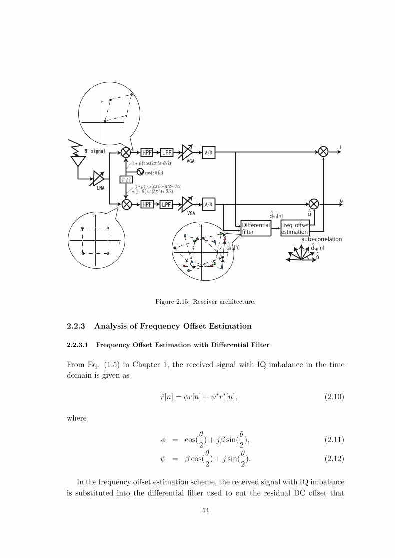
Figure 2.15: Receiver architecture.
2.2.3 Analysis of Frequency Offset Estimation
2.2.3.1 Frequency Offset Estimation with Differential Filter
From Eq. (1.5) in Chapter 1, the received signal with IQ imbalance in the time
domain is given as
r[n] = φr[n] + ψ∗r∗[n], (2.10)
where
φ = cos(θ
2) + jβ sin(
θ
2), (2.11)
ψ = β cos(θ
2) + j sin(
θ
2). (2.12)
In the frequency offset estimation scheme, the received signal with IQ imbalance
is substituted into the differential filter used to cut the residual DC offset that
54

passes through the HPF. The n-th output dSP [n] after the differential filter is
dSP [n] = rSP [n] − rSP [n − 1]
= φ{rSP [n] − rSP [n − 1]} + ψ∗{r∗SP [n] − r∗SP [n − 1]}, n ≥ 1
(2.13)
where
rSP [n] = φrSP [n] + ψ∗r∗SP [n], (2.14)
rSP [n] is the n-th signal with the frequency offset in the STSP period. In the
STSP, the short preamble with the period of N/4 samples are repeated 10 times.
From Eq. (2.13), the auto-correlation value used for frequency offset estimation
with the IQ imbalance is given as
d∗SP [n]dSP [n +
N
4]
= [φ{rSP [n] − rSP [n − 1]} + ψ∗{r∗SP [n] − r∗SP [n − 1]}]∗
·[φ{rSP [n +N
4] − rSP [n +
N
4− 1]} + ψ∗{r∗SP [n +
N
4] − r∗SP [n +
N
4− 1]}]
= ρ1[n] + ρ2[n] + ρ3[n] + ρ4[n] + ρ5[n]
+Δ(|φ|2vv∗) + Δ(φ∗ψ∗v∗) + Δ(φ∗ψ∗(v∗)2)
+Δ(φψv) + Δ(φψv2) + Δ(|ψ|2v) + Δ(|ψ|2v∗) + Δ(|ψ|2vv∗), (2.15)
where,
ρ1[n] = |φ|2∣∣∣sSP [n] exp(j
2πα
Nn) − sSP [n − 1] exp(j
2πα
N(n − 1))
∣∣∣2 exp(j2πα
4),
(2.16)
ρ2[n] = φ∗ψ∗{s∗SP [n] exp(−j2πα
Nn) − s∗SP [n − 1] exp(−j
2πα
N(n − 1))}2 exp(−j
2πα
4),
(2.17)
ρ3[n] = φψ{sSP [n] exp(j2πα
Nn) − sSP [n − 1] exp(j
2πα
N(n − 1))}2 exp(j
2πα
4),
(2.18)
ρ4[n] = |ψ|2∣∣∣sSP [n] exp(j
2πα
Nn) − sSP [n − 1] exp(j
2πα
N(n − 1))
∣∣∣2 exp(−j2πα
4),
(2.19)
55

ρ5[n] = |φ|2v[n +N
4]{s∗SP [n] exp(−j
2πα
Nn) − s∗SP [n − 1] exp(−j
2πα
N(n − 1))}
− |φ|2v[n +N
4− 1]{s∗SP [n] exp(−j
2πα
Nn) − s∗SP [n − 1] exp(−j
2πα
N(n − 1))}
+ |φ|2v∗[n]{sSP [n] exp(j2πα
Nn) − sSP [n − 1] exp(j
2πα
N(n − 1))} exp(j
2πα
4)
− |φ|2v∗[n − 1]{sSP [n] exp(j2πα
Nn) − sSP [n − 1] exp(j
2πα
N(n − 1))} exp(j
2πα
4),
(2.20)
and Δ(|φ|2vv∗), Δ(φ∗ψ∗v∗), Δ(φ∗ψ∗(v∗)2), Δ(φψv), Δ(φψv2), Δ(|ψ|2v), Δ(|ψ|2v∗),and Δ(|ψ|2vv∗) are the terms including the noise components that are |φ|2vv∗,φ∗ψ∗v∗, φ∗ψ∗(v∗)2, φψv, φψv2, |ψ|2v, |ψ|2v∗, and |ψ|2vv∗, respectively. Also, sSP [n]
is the n-th sample of the STSP symbol.
The estimated frequency offset with STSP, α, is given as
α =4
2πarg{
9N4
−1∑n=N
d∗SP [n]dSP [n +
N
4]}, (2.21)
where n = N corresponds to the time index of the first symbol of t5 and n = 9N4−1
corresponds to the time index of the last symbol of t9. Here, the STSP symbols
from t5 to t10 are used for frequency offset estimation. The auto-correlations be-
tween t1 and t4 are not used because of passible gain shift of the LNA [2.19]. The
total amount of the distortion in the sum of the auto-correlations depends on the
number of the samples for summation and the waveform of the preamble signals.
2.2.3.2 MSE Performance
To evaluate the performance of frequency offset estimation with the differential
filter, the MSE is analyzed. From Eq. (2.12), the absolute value of ψ is relatively
small. Also |v|2 is negligible as compared with the signal amplitude if the SNR is
large enough. Therefore, Δ terms in Eq. (2.15) are neglected and it is assumed
that Eq. (2.15) consists of 5 terms from ρ1[n] to ρ5[n], which indicates the effect
of IQ imbalance. Vectors corresponding to those terms are given in Fig. 2.16.
Without IQ imbalance, Eq. (2.15) has only one vector, ρ1[n]. ρ2[n] is conjugate
of ρ3[n]. Thus the addition of ρ2[n] and ρ3[n] resolves in a vector with only a real
component. ρ5[n] contains the noise components. The summation of terms from
ρ2[n] to ρ5[n] deteriorates the accuracy of frequency offset estimation.
56

Figure 2.16: Vectors representation of auto-correlation.
Based on Eq. (2.15), the error of the estimation is given as
α − α = α − 4
2π[arg{
9N4
−1∑n=N
ρ1[n] + ρ2[n] + ρ3[n] + ρ4[n] + ρ5[n]}]. (2.22)
The variance of ρ5[n] is expressed as
σ2v = E{|
9N4
−1∑n=N
ρ5[n]|2}
= E{|9N4
−1∑n=N
ρ′[n] + ρ′′[n] + ρ′′′[n] + ρ′′′′[n]|2}.
(2.23)
where from Eq. (2.20),
ρ′[n] = |φ|2v[n +N
4]{s∗SP [n] exp(−j
2πα
Nn) − s∗SP [n − 1] exp(−j
2πα
N(n − 1))},
(2.24)
ρ′′[n] = −|φ|2v[n +N
4− 1]{s∗SP [n] exp(−j
2πα
Nn) − s∗SP [n − 1] exp(−j
2πα
N(n − 1))},
(2.25)
ρ′′′[n] = |φ|2v∗[n]{sSP [n] exp(j2πα
Nn) − sSP [n − 1] exp(j
2πα
N(n − 1))} exp(j
2πα
4),
(2.26)
57

Figure 2.17: Cancelation in auto-correlation.
ρ′′′′[n] = −|φ|2v∗[n − 1]{sSP [n] exp(j2πα
Nn) − sSP [n − 1] exp(j
2πα
N(n − 1))} exp(j
2πα
4).
(2.27)
Here,
ρ′[n] = ρ′′′[n +N
4], (2.28)
ρ′′[n] = ρ′′′′[n +N
4]. (2.29)
As a result, due to ρ5[n], the STSP symbols from t6 to t9 are canceled and only
the following terms remains after the summation as shown in Fig. 2.17.
9N4
−1∑n=N
ρ5[n]
=
5N4
−1∑n=N
[|φ|2v∗[n]{sSP [n] exp(j2πα
Nn) − sSP [n − 1] exp(j
2πα
N(n − 1))} exp(j
2πα
4)
−|φ|2v∗[n − 1]{sSP [n] exp(j2πα
Nn) − sSP [n − 1] exp(j
2πα
N(n − 1))} exp(j
2πα
4)]
+
9N4
−1∑n=2N
[|φ|2v[n +N
4]{s∗SP [n] exp(−j
2πα
Nn) − s∗SP [n − 1] exp(−j
2πα
N(n − 1))}
−|φ|2v[n +N
4− 1]{s∗SP [n] exp(−j
2πα
Nn) − s∗SP [n − 1] exp(−j
2πα
N(n − 1))}].
(2.30)
Thus, Eq. (2.23) is approximated as
σ2v = 4 · N
4· Ed · 1
2 · SNR, (2.31)
58

where SNR = Es/σ2n, Es = E{|sSP [n]|2}, and Ed = E{|rSP [n] − rSP [n − 1]|2}.
Here, it is assumed that
|φ|2 ≈ 1, (2.32)
and
|9N4
−1∑n=N
{ρ1[n] + ρ2[n] + ρ3[n] + ρ4[n]}| � |9N4
−1∑n=N
ρ5[n]|.
(2.33)
With the above approximations, the MSE of frequency offset estimation is then
obtained as
E{|α − α|2}
= |α − 4
2π[arg{
9N4
−1∑n=N
ρ1[n] + ρ2[n] + ρ3[n] + ρ4[n]}]|2
+σ2
v
E{|∑ 9N4
−1
n=N ρ1[n] + ρ2[n] + ρ3[n] + ρ4[n]|2}
= |α − 4
2π[arg{
9N4
−1∑n=N
ρ1[n] + ρ2[n] + ρ3[n] + ρ4[n]}]|2 +2
5 · SNR. (2.34)
The normalized MSE of frequency offset estimation, NMSE{α}, is given as
NMSE{α} =E{|α − α|2}
α2. (2.35)
2.2.4 Numerical Results
2.2.4.1 Simulation Conditions
The MSE of the frequency offset estimation is evaluated through computer sim-
ulation. The simulation conditions are shown in Table 2.2. Information bits are
modulated with QPSK on each subcarrier. The number of DFT/IDFT points is
set to 64 while 52 subcarriers are used for the LTSP symbols, which follows the
IEEE802.11a/g standard. The 1st order butterworth filter is employed as the Rx
HPF. The cutoff frequency of the received HPF is set to 10[kHz]. The normalized
frequency offset is from 0.1 to 0.5. The mismatch of the amplitude is set at a range
of 0.01 to 0.05 and the mismatch of the phase is set at a range of 1 to 5[degrees]
[2.21].
59

Table 2.2: Simulation conditions.
Trial number 10,000 timesModulation scheme QPSK+OFDM
Number of subcarrier 64Number of data subcarrier 52
Channel AWGNRx HPF 1st order Butterworth filter
fB=10[kHz]Normalized frequency offset 0.1-0.5
Gain mismatch β 0.01-0.05Phase mismatch θ 1-5 [degrees]
Figure 2.18: MSE vs. SNR (β=0.05, θ=5[degrees]).
2.2.4.2 MSE Performance of Frequency Offset Estimation under IQ imbalance
Fig. 2.18 shows the relationship between the MSE performance and the SNR. Here,
the gain mismatch is set to 0.05, the phase mismatch is set to 5[degrees]. The MSE
curves for the theoretical analysis is close to the numerical results obtained through
computer simulation when the SNR is more than 10[dB]. The difference between
the analysis and simulation is due to the noise components in Eq. (2.15) that are
neglected in the MSE derivation.
Fig. 2.19 shows the MSE performance of frequency offset estimation when the
60

Figure 2.19: MSE vs. normalized frequency offset (θ=5[degrees], β=0.05).
normalized frequency offset is varied. It is assumed that the gain mismatch β is
0.05, the phase mismatch θ is 5[degrees], and the SNR is 20, 25, and 30[dB]. The
MSE curves for the theoretical analysis are very close to the simulated curves. It
can be seen from Fig. 2.19 that the normalized MSE performance improves as
the frequency offset increases. The dependency of the MSE on the normalized
frequency offset is due to the amount of the residual distortion caused by IQ im-
balance after the sum of the auto-correlation samples in Eq. (2.21). The distortion
changes according to the waveform of the preamble symbols with frequency off-
set as shown in Eq. (2.15). This fluctuation is observed without thermal noise
(SNR = ∞).
Fig. 2.20 shows the MSE performance vs. gain mismatch. Here, the normalized
frequency offset is set to 0.3, the phase mismatch is set to 5[degrees], and the SNR
is 20, 25, and 30[dB]. The MSE curves for the theoretical analysis are very close to
the ones obtained through computer simulation. As the gain mismatch increases,
the MSE performance of frequency offset estimation is deteriorated.
Fig. 2.21 shows the MSE performance vs. phase mismatch. Here, the normal-
ized frequency offset is set to 0.3, the gain mismatch is set to 0.05, and the SNR
is 20, 25, and 30[dB]. Again, the MSE curves for the theoretical analysis are very
close to the ones for the computer simulation. As the phase mismatch increases,
the MSE increases.
61

Figure 2.20: MSE vs. gain mismatch (normalized freq. offset=0.3, θ=5[degrees]).
Figure 2.21: MSE vs. phase mismatch (normalized freq. offset=0.3, β=0.05).
2.2.5 Conclusions
In this section, the performance of the frequency offset estimation with the differ-
ential filter in the presence of IQ imbalance has been analyzed. Frequency offset is
62

estimated through the auto-correlation of the preamble symbols that goes through
the differential filter. IQ imbalance deteriorates the accuracy of the frequency offset
estimation scheme. The theoretical curves matches the numerical results obtained
through the computer simulation when the SNR is more than 10[dB]. It has been
shown that the MSE varies according to the amount of frequency offset. This is
due to the residual distortion of the auto-correlation caused by IQ imbalance and
it depends on the waveform of the preamble symbols.
2.3 Time Domain IQ Imbalance Estimation Scheme in the
Presence of Frequency Offset and Time-varying DC
Offset for Direct Conversion Receivers
A direct conversion architecture reduces the cost and power consumption of a
receiver. However, the direct conversion receiver may suffer from DC offset, fre-
quency offset, and IQ imbalance. This section presents a time domain IQ imbalance
estimation scheme for OFDM direct conversion receivers. The proposed IQ imbal-
ance estimation scheme operates in the presence of the time-varying DC offset and
the frequency offset. The proposed scheme calculates the IQ imbalance from a
simple equation. It employs the knowledge of the preamble symbols of the IEEE
802.11 a/g standards while it does not require the impulse response of the channel.
2.3.1 Introduction
In IEEE 802.11a/g, the high data rate transmission is realized because an OFDM
modulation scheme is used as the 2nd modulation. At the receiving end, a direct
conversion architecture has been implemented, which reduces the cost and power
consumption of the receiver. However, as mentioned in Chapter 1, OFDM direct
conversion receivers may suffer from the DC offset, the frequency offset, and the IQ
imbalance [2.1]-[2.22]. These distortions deteriorate the quality of the demodulated
signal. They should be compensated within the received frame since the amount
of mismatch depends on the transmitter.
Several joint compensation schemes have been presented [2.23]-[2.21]. In [2.23],
the frequency offset and the IQ imbalance are estimated using a nonlinear least-
squares scheme. This scheme requires the covariance matrix of the received sam-
ples. In [2.4], the IQ imbalance as well as the frequency offset and the DC offset are
estimated using the maximum likelihood criterion. Although this scheme achieves
a performance close to the Cramer-Rao bound, it requires a large amount of com-
63
putation and channel response. In [2.24], a frequency offset and IQ imbalance
estimation scheme is proposed on the basis of simple calculation. The scheme in
[2.21] carries out frequency offset and IQ imbalance estimation in the time domain.
However, these schemes assume the absence of DC offset. Blind estimation and
compensation schemes in the time domain have also been proposed [2.25]-[2.27].
Although the amount of computation for each iteration of the adaptive processes
is relatively small, these schemes do not assume the time-varying DC offset. If the
time-varying DC offset is present, the convergence time may exceed the duration
of the short preamble.
The level of DC offset varies due to the gain switching in the LNA. However,
none of the above studies take into account the time-varying DC offset, frequency
offset, and IQ imbalance at the same time.
In this section, a novel time domain IQ imbalance estimation scheme is inves-
tigated allowing for the time-varying DC offset and the frequency offset. In the
proposed scheme, the differential filter is employed to remove the time-varying DC
offset. In previous sections, it has been shown that the differential filter effectively
estimates the frequency offset in the presence of the time-varying DC offset [2.19]-
[2.29]. In the proposed scheme, from the output of the differential filter, the IQ
imbalance as well as the frequency offset is estimated from a simple equation. The
proposed scheme employs the knowledge of the preamble symbols of the IEEfE
802.11a/g standards, while it does not require the impulse response of the chan-
nel. Therefore, this scheme is suitable for low-cost and low-power-consumption
receivers.
This section is organized as follows. Subsection 2.3.2 gives the system model
and the IQ imbalance model. In subsection 2.3.3, the frequency offset estimation
using the differential filter is explained. Subsection 2.3.4 describes the proposed
IQ imbalance estimation. In subsection 2.3.5 numerical results obtained through
computer simulation are presented. Subsection 2.3.6 gives our conclusions.
2.3.2 System Model
In this section, the IQ imbalance estimation is employed on the training sequence of
IEEE 802.11a/g [2.8][2.9]. To maintain the received signal amplitude at a suitable
fixed level, the AGC is used. In a WLAN receiver, the AGC controls the receiver
gain in the middle of the STSP. In the 802.11a/g standards, gain control of more
than 50dB is required [2.6]. The assumed RF architecture in this section is shown
in Fig. 2.23. As shown in the figure, gain control is applied in both the LNA and
the VGAs. Here, an LNA with two gain modes is assumed [2.7]-[2.14]. This type
64

Figure 2.22: DC offset and the output of differential filter.
of LNA has been discussed in [2.7] and [2.11]. The VGAs at baseband compensate
the rest of the required gain.
In the direct conversion receiver, the DC offset may be eliminated by the HPFs,
as shown in Fig. 2.23 [2.1][2.7]. However, as the gain of the LNA changes, the
DC offset level varies [2.12]. Figures 2.22 (a), (b), and (c) show the received signal
(absolute value) of the training sequence preamble when the gain of the LNA is
changed. At the beginning of the STSP, the gain of the LNA is set to the maximum
because the power of the received signal is unknown to the receiver. If the power of
the received signal is sufficiently large, the LNA is switched to the low-gain mode
between t4 and t5. The DC offset level then decreases rapidly and the fluctuating
DC offset level is input into the HPF. Here, the fluctuation of the DC offset level
is modeled as a two-step function as shown in Fig. 2.22 (a) [2.12]. The transient
response of the HPF due to the fluctuation of the DC offset level appears at
65

Figure 2.23: Receiver architecture.
the output of the HPF as shown in Fig. 2.22 (b). The component deteriorates
the accuracy of frequency offset estimation and IQ imbalance estimation. In the
proposed scheme, the transient response is removed using the differential filter. The
cutoff frequency of the HPF is set to a relatively low value so as not to eliminate the
data subcarriers adjacent to the DC subcarrier in the data period. Since the cutoff
frequency of the HPF is low, the transient response decreases gradually. Thus, the
differential filter can suppress the effect of the residual DC offset as shown in Fig.
2.22 (c).
2.3.3 Frequency Offset Estimation
2.3.3.1 Frequency Offset, DC Offset, and IQ Imbalance Model
In order to clarify the signal model with the frequency offset, the DC offset, and
the IQ imbalance, the following explanation omits the noise term, v[k], in Eq.
(1.1) for simplicity. From Eq. (1.5) in Chapter 1, the received signal with the IQ
imbalance in the time domain is given as
r[n] = φr[n] + ψ∗r∗[n] + δ[n], (2.36)
66

where
φ = cos(θ
2) + jβ sin(
θ
2), (2.37)
ψ = β cos(θ
2) + j sin(
θ
2), (2.38)
and δ[n] is the DC offset that occurs at the mixer.
The frequency offset is estimated in the presence of the time-varying DC offset
and the IQ imbalance. After coarse estimation, the LTSP symbols are used for
channel estimation for each subcarrier.
2.3.3.2 Frequency Offset Estimation Using Differential Filter
In this frequency offset estimation scheme, the received signal with IQ imbalance
is substituted into the differential filter used to eliminate the residual DC offset
that passes through the HPF. The n-th output dSP [n] after the differential filter is
dSP [n] = rSP [n] − rSP [n − 1]
= φ{rSP [n] − rSP [n − 1]} + ψ∗{r∗SP [n] − r∗SP [n − 1]} + Δδ[n, n − 1], n ≥ 1,
(2.39)
where
rSP [n] = φrSP [n] + ψ∗r∗SP [n], (2.40)
rSP [n] is the n-th signal with the frequency offset in the STSP period, and Δδ[n, n−1] is the difference between the n-th and [n−1]-th residual DC offsets. In the STSP,
a short preamble with a period of N/4 samples is repeated 10 times. From Eq.
(2.39), the autocorrelation value for frequency offset estimation with the DC offset
67

and the IQ imbalance is given by
d∗SP [n]dSP [n +
N
4]
= |φ|2|rSP [n +N
4] − rSP [n +
N
4− 1]|2 exp(j
2πα
4)
(2.41a)
+φ∗ψ∗(rSP [n +N
4] − rSP [n +
N
4− 1])2 exp(−j
2πα
4)
(2.41b)
+φψ(rSP [n +N
4] − rSP [n +
N
4− 1])2 exp(j
2πα
4)
(2.41c)
+|ψ|2|rSP [n +N
4] − rSP [n +
N
4− 1]|2 exp(−j
2πα
4)
(2.41d)
+O(Δδ[n +N
4, n +
N
4− 1], Δδ[n, n − 1]). (2.41e)
Here, O(Δδ[n+ N4, n+ N
4−1], Δδ[n, n−1]) is the product of Δδ[n+ N
4, n+ N
4−1] and
Δδ[n, n−1]∗, N is the number of samples, and α is the normalized frequency offset
in one OFDM symbol period. By averaging over 10 STSP symbols, the normalized
frequency offset α is estimated from the first term (2.41a). The additional MSE in
frequency offset estimation due to the IQ imbalance is caused by the terms given
in (2.41b), (2.41c), and (2.41d). However, it is less than 10−3 of the square of
the frequency offset [2.29]. Thus, the IQ imbalance is neglected at this stage for
estimation of the frequency offset.
2.3.4 IQ Imbalance Estimation
2.3.4.1 IQ Imbalance Estimation
The IQ imbalance is also estimated from the outputs of the differential filter. From
Eq. (2.39), the 3 preamble symbols repeated in N/4 samples in the STSP can be
expressed as
dSP [n − N
4] = rSP [n − N
4] − rSP [n − N
4− 1]
= φ{rSP [n] − rSP [n − 1]} exp(−j2πα
4)
+ ψ∗{r∗SP [n] − r∗SP [n − 1]} exp(j2πα
4)
= φdSP [n]γ−1 + ψ∗d∗SP [n]γ, (2.42)
68
dSP [n] = rSP [n] − rSP [n − 1]
= φ{rSP [n] − rSP [n − 1]} + ψ∗{r∗SP [n] − r∗SP [n − 1]}= φdSP [n] + ψ∗d∗
SP [n], (2.43)
dSP [n +N
4] = rSP [n +
N
4] − rSP [n +
N
4− 1]
= φ{rSP [n +N
4] − rSP [n +
N
4− 1]}
+ ψ∗{r∗SP [n +N
4] − r∗SP [n +
N
4− 1]}
= φ{rSP [n] − rSP [n − 1]} exp(j2πα
4)
+ ψ∗{r∗SP [n] − r∗SP [n − 1]} exp(−j2πα
4)
= φdSP [n]γ + ψ∗d∗SP [n]γ−1. (2.44)
Here,
dSP [n] = rSP [n] − rSP [n − 1], (2.45)
γ = exp(j2πα
4). (2.46)
Solving Eqs. (2.42), (2.43), and (2.44) as simultaneous equations, the following
equation is derived.
dSP [n − N4] − dSP [n]γ−1
(dSP [n]γ−1 − dSP [n + N4])∗
=ψ∗
φ∗ = ε. (2.47)
Here, with the assumption of small θ, φ and ψ are approximated as
φ = cos(θ
2) + jβ sin(
θ
2) ≈ 1 + jβ
θ
2, (2.48)
ψ = β cos(θ
2) + j sin(
θ
2) ≈ β + j
θ
2, (2.49)
using the first-order approximation of the Taylor expansion. Thus, Eq. (2.47)
becomesβ − j θ
2
1 − jβ θ2
≈ εI + jεQ. (2.50)
β and θ can then be calculated as follows.
β ≈ 2εI
2 − εQθ, (2.51)
69

θ ≈−(ε2
I + ε2Q − 1) −
√(ε2
I + ε2Q − 1)2 + 4ε2
Q
εQ
. (2.52)
To obtain ε in Eq. (2.47), α in Eq. (2.46) is substituted with the value estimated
in Section 2.3.3.
In terms of complexity, the estimation of ε requires the following number of
calculations;
Cε = Nsp × [2·Cadd + 1·Cmult] + 1·Cdiv, (2.53)
where Cadd, Cmult, and Cdiv are the numbers of complex additions, multiplications,
and divisions, respectively, and Nsp represents the number of samples in the STSP.
The complexity is almost equivalent to the conventional scheme in [2.21].Note that, similar to [2.21], the proposed scheme works well if α is more than
0.1. This can be understood by taking the noise term into consideration in Eq.(2.47). If the noise is included, the left side of Eq. (2.47) turns to
ψ∗{s∗SP [n] exp(−j 2πα
N n) − s∗SP [n − 1] exp(−j 2πα
N [n − 1])}(γ − γ−1) + O(φ, ψ, γ−1, v[n − N4 − 1], v[n − N
4 ], v[n − 1], v[n])
φ∗{s∗SP [n] exp(−j 2πα
N n) − s∗SP [n − 1] exp(−j 2πα
N [n − 1])}(γ − γ−1) + O(φ, ψ, γ, v[n − 1], v[n], v[n + N4 − 1], v[n + N
4 ]).
(2.54)
Here, O(φ, ψ, γ−1, v[n− N4− 1], v[n− N
4], v[n− 1], v[n]) is the product of φ, ψ, γ−1,
v[n− N4−1], v[n− N
4], v[n−1], v[n]. O(φ, ψ, γ, v[n−1], v[n], v[n+ N
4−1], v[n+ N
4])
is also the product of φ, ψ, γ, v[n−1], v[n], v[n+ N4−1], v[n+ N
4]. If the frequency
offset α is small, the term (γ − γ−1) approaches 0. The left side of Eq. (2.47) is
then approximated as
dSP [n − N4] − dSP [n]γ−1
(dSP [n]γ−1 − dSP [n + N4])∗
≈ O(φ, ψ, γ, v[n − N4− 1], v[n − N
4], v[n − 1], v[n])
O(φ, ψ, γ, v[n − 1], v[n], v[n + N4− 1], v[n + N
4])
. (2.55)
Thus, the estimation of IQ imbalance becomes inaccurate. In this case, the time
difference among the outputs of the differential filter in Eqs. (2.42), (2.43), and
(2.44) should be set to longer than N/4. The effective frequency offset then in-
creases although the number of samples required to calculate Eq. (2.47) decreases.
2.3.4.2 IQ Imbalance Compensation
In the LTSP and the following data period, IQ imbalance is compensated on the
basis of the phase mismatch and gain mismatch estimated in the STSP. By con-
70

Table 2.3: Simulation conditions.Number of trials 10,000 times
Modulation scheme Preamble: QPSK+OFDMData: 64QAM+OFDM
Number of subcarriers 64Number of data subcarriers 52
Channel AWGNRx HPF 1st-order Butterworth filter
fc=10[kHz]Normalized DC offset 35/15[dB]
Normalized frequency offset α 0.3Gain mismatch β 0.01-0.05Phase mismatch θ 0-5 [degrees]
solidating Eqs. (1.7) and (1.8) into a system of equations, we arrive at[rdI
rdQ
]=
[(1 + β) cos( θ
2) −(1 + β) sin( θ
2)
−(1 − β) sin( θ2) (1 − β) cos( θ
2)
][rdI
rdQ
]
= Ω
[rdI
rdQ
], (2.56)
where rdI, rdQ
, rdI, and rdQ
are the I and Q components of the received signal with
and without IQ imbalance, respectively. The IQ imbalance is compensated using
Ω−1.
2.3.5 Simulation Results
2.3.5.1 Simulation Conditions
The MSE of the IQ imbalance estimation is evaluated through computer simula-
tion. The simulation conditions are shown in Table 2.3. The number of trials is
10,000 times. Information bits are modulated with QPSK in the preamble period
and 64 quadrature amplitude modulation (QAM) in the data period on each sub-
carrier. The number of DFT/IDFT points is set to 64, while 48 subcarriers are
used for the data subcarriers and 4 subcarriers are used for the pilot subcarriers,
which follows the IEEE 802.11a/g standards. As a channel model, AWGN channel
is assumed. A 1st-order Butterworth filter is employed as the HPF. The cutoff
frequency of the HPF is set to 10[kHz]. The normalized frequency offset, α, is 0.3.
The gain mismatch is set from 0.01 to 0.05 and the phase mismatch is varied from
0 to 5[degrees] [2.21].
71

Figure 2.24: Normalized MSE performance of phase mismatch estimation vs. phase mismatch(β=0.05, normalized freq. offset = 0.3).
The gain of the LNA can be selected between 35 and 15[dB] [2.15]. The isolation
between the LO output and the LNA input is assumed to be -60[dB]. Therefore,
if the power of the LO signal is set to 0[dBm], the DC offset level is -25/-45[dBm].
On the other hand, the received signal power is set to -53[dBm], which is equiv-
alent to -70[dBm] on each subcarrier in the LTSP. In this case, the DC offset is
10[dB] larger than the signal power on each subcarrier.
2.3.5.2 Normalized MSE Performance of Phase Mismatch Estimation vs. PhaseMismatch
Figure 2.24 shows the normalized MSE performance of phase mismatch estimation.
In this figure, ‘Conventional’ refers to the IQ imbalance estimation scheme in the
time domain presented in [2.21]. The gain mismatch β is set to 0.05 and the
normalized frequency offset α is set to 0.3. In Fig. 2.24, the proposed scheme has
better estimation performance.The reason for this is that the conventional scheme
suffers from the residual DC offset. In this figure, the MSE improves as the phase
mismatch increases. This is because the MSE is normalized by the mismatch
θ. Furthermore, the normalized MSE performance improves as Eb/N0 increases
72
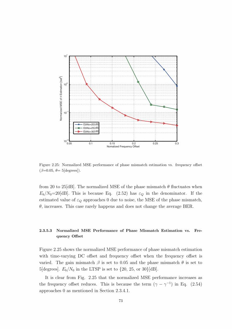
Figure 2.25: Normalized MSE performance of phase mismatch estimation vs. frequency offset(β=0.05, θ= 5[degrees]).
from 20 to 25[dB]. The normalized MSE of the phase mismatch θ fluctuates when
Eb/N0=20[dB]. This is because Eq. (2.52) has εQ in the denominator. If the
estimated value of εQ approaches 0 due to noise, the MSE of the phase mismatch,
θ, increases. This case rarely happens and does not change the average BER.
2.3.5.3 Normalized MSE Performance of Phase Mismatch Estimation vs. Fre-quency Offset
Figure 2.25 shows the normalized MSE performance of phase mismatch estimation
with time-varying DC offset and frequency offset when the frequency offset is
varied. The gain mismatch β is set to 0.05 and the phase mismatch θ is set to
5[degrees]. Eb/N0 in the LTSP is set to {20, 25, or 30}[dB].
It is clear from Fig. 2.25 that the normalized MSE performance increases as
the frequency offset reduces. This is because the term (γ − γ−1) in Eq. (2.54)
approaches 0 as mentioned in Section 2.3.4.1.
73

Figure 2.26: Normalized MSE performance of gain mismatch estimation (θ= 5[degrees], normal-ized freq. offset=0.3).
2.3.5.4 Normalized MSE Performance of Gain Mismatch Estimation
Figure 2.26 shows the normalized MSE performance of the gain mismatch estima-
tion with the time-varying DC offset and frequency offset when the gain mismatch
value is varied. The phase mismatch θ is set to 5[degrees] and the normalized
frequency offset α is set to 0.3. Eb/N0 in the LTSP is set to {20, 25, or 30}[dB].
It can be seen from Fig. 2.26 that the normalized MSE performance improves
as the gain mismatch increases. This is because the MSE is normalized by the gain
mismatch β. As Eb/N0 increases to 10[dB], the normalized MSE is reduced by a
factor of about 10.
2.3.5.5 BER Performance
The BER performance versus Eb/N0 in the AWGN channel is shown in Fig. 2.27.
The simulation conditions are the same as those with the static DC offset. From
Fig. 2.27, it can be concluded that the performance degradation due to the pro-
posed scheme is about 4[dB]. This plot is simulated using 1st order interpolation
for phase compensation using pilot subcarriers. 125 OFDM symbols are transmit-
74

Figure 2.27: BER performance with 1st order interpolation (normalized freq. offset=0.3, β=0.05,θ=5[degrees]).
ted for each packet and 64QAM is assumed. The number of DFT/IDFT points
is set to 64. The OFDM receiver is considered with normalized frequency offset
α = 0.3, gain imbalance β = 0.05, and phase mismatch θ = 5[degrees].
‘With Foffset and IQ Compe (Conventional)’ refers to the case with frequency
offset compensation and the IQ imbalance compensation presented in [2.21]. ‘With-
out Compe’ represents the simulation in the case of no frequency offset compensa-
tion or IQ imbalance compensation, ‘With Foffset Compe’ refers to frequency offset
compensation, and ‘With Foffset and IQ Compe’ refers to the case of frequency
offset compensation and IQ imbalance compensation. In addition, ‘Reference’ rep-
resents the simulation when phase compensation by pilot subcarriers is carried out
under the frequency offset and the IQ imbalance. In each OFDM symbol, following
the IEEE 802.11 a/g standards, 4 pilot subcarriers are inserted. ‘Theory’ is the
theoretical BER curve for 64QAM.
As shown in this figure, the proposed scheme exhibits superior estimation perfor-
mance since the conventional scheme suffers from the residual DC offset. Moreover,
neither frequency offset compensation nor IQ imbalance compensation degrades
the performance significantly. Comparing the proposed scheme with theoretical
75

results, there is a difference of 8[dB], in which 4[dB] of the difference is due to
nonideal channel equalization by the pilot subcarriers. Thus, the BER using the
proposed IQ imbalance estimation scheme exhibits about 4[dB] degradation with
the large DC offset, the frequency offset, and the IQ imbalance. However, our
proposed scheme has less complexity than existing algorithms.
2.3.6 Conclusions
The direct conversion receiver has disadvantages such as the DC offset, the fre-
quency offset, and the IQ imbalance. In this section, a low-complexity IQ imbal-
ance estimation scheme allowing for the time-varying DC offset and the frequency
offset has been proposed. The IQ imbalance is calculated using a simple equation
without requiring the impulse response of the channel. Therefore, the proposed
scheme is suitable for low-cost and low-power-consumption terminals. Computer
simulations show that the BER performance using the proposed IQ imbalance es-
timation scheme is satisfactory when Eb/N0 is more than 20[dB], in which 64QAM
is used for the 1st modulation. The system exhibits degradation of about 4[dB]
with the large time-varying DC offset, the frequency offset, and the IQ imbalance.
2.4 Frequency Domain IQ Imbalance Estimation Scheme
in the Presence of DC Offset and Frequency Offset
The direct conversion receivers in OFDM systems suffer from DC offset, frequency
offset, and IQ imbalance. We have proposed the IQ imbalance estimation scheme
in the presence of DC offset and frequency offset, which uses the preamble signals
in the time domain as mentioned in Section 2.3. In this scheme, the DC offset
is eliminated by the differential filter. However, the accuracy of IQ imbalance
estimation is deteriorated when the frequency offset is small. To overcome this
problem, a new IQ imbalance estimation scheme in the frequency domain has been
proposed in this chapter. The IQ imbalance is estimated with pilot subcarriers.
Numerical results obtained through computer simulation show that estimation
accuracy and BER performance can be improved even if the frequency offset is
small.
2.4.1 Introduction
As mentioned in Chapter 1, OFDM direct conversion receivers may suffer from the
DC offset, the frequency offset, and the IQ imbalance [2.1][2.2]. These distortions
76
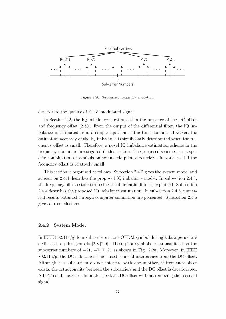
Figure 2.28: Subcarrier frequency allocation.
deteriorate the quality of the demodulated signal.
In Section 2.2, the IQ imbalance is estimated in the presence of the DC offset
and frequency offset [2.30]. From the output of the differential filter, the IQ im-
balance is estimated from a simple equation in the time domain. However, the
estimation accuracy of the IQ imbalance is significantly deteriorated when the fre-
quency offset is small. Therefore, a novel IQ imbalance estimation scheme in the
frequency domain is investigated in this section. The proposed scheme uses a spe-
cific combination of symbols on symmetric pilot subcarriers. It works well if the
frequency offset is relatively small.
This section is organized as follows. Subection 2.4.2 gives the system model and
subsection 2.4.4 describes the proposed IQ imbalance model. In subsection 2.4.3,
the frequency offset estimation using the differential filter is explained. Subsection
2.4.4 describes the proposed IQ imbalance estimation. In subsection 2.4.5, numer-
ical results obtained through computer simulation are presented. Subsection 2.4.6
gives our conclusions.
2.4.2 System Model
In IEEE 802.11a/g, four subcarriers in one OFDM symbol during a data period are
dedicated to pilot symbols [2.8][2.9]. These pilot symbols are transmitted on the
subcarrier numbers of −21, −7, 7, 21 as shown in Fig. 2.28. Moreover, in IEEE
802.11a/g, the DC subcarrier is not used to avoid interference from the DC offset.
Although the subcarriers do not interfere with one another, if frequency offset
exists, the orthogonality between the subcarriers and the DC offset is deteriorated.
A HPF can be used to eliminate the static DC offset without removing the received
signal.
77

2.4.3 Frequency Offset Estimation Using Differential Filter
In this frequency offset estimation scheme, the received signal with IQ imbalance
is substituted into the differential filter used to eliminate the residual DC offset
that passes through the HPF. The n-th output, dSP [n], after the differential filter
is
dSP [n] = rSP [n] − rSP [n − 1]
= φ{rSP [n] − rSP [n − 1]} + ψ∗{r∗SP [n] − r∗SP [n − 1]} + Δδ[n, n − 1], n ≥ 1,
(2.57)
where
rSP [n] = φrSP [n] + ψ∗r∗SP [n], (2.58)
rSP [n] is the n-th signal with the frequency offset in the STSP period, and Δδ[n, n−1] is the difference between the n-th and [n − 1]-th residual DC offsets. In IEEE
802.11a/g standards, the coarse frequency offset estimation is carried out in STSP
and the fine frequency offset estimation is carried out in LTSP [2.8][2.9]. In this
section, the frequency offset estimation is calculated from auto-correlation value
of STSP and LTSP received signals with IQ imbalance and frequency offset. From
Eq. (2.21), the estimated frequency offset with STSP, α′, is given as
α′ =4
2πarg{
9N4
−1∑n=N
d∗SP [n]dSP [n +
N
4]}, (2.59)
where n = N corresponds to the time index of the first symbol of t5 and n = 9N4−1
corresponds to the time index of the last symbol of t9. Here, the STSP symbols
from t5 to t10 are used for frequency offset estimation. The auto-correlations be-
tween t1 and t4 are not used because of passible gain shift of the LNA [2.28].
The coarse frequency offset value obtained from STSP is used for compensation in
LTSP. The estimated frequency offset with LTSP, α′′, is then given as
α′′ =1
2πarg{
N−1∑n=1
d∗LP [n]dLP [n + N ]}, (2.60)
where dLP [n] is the n-th output of the differential filter in LTSP. As a result, the
fine frequency estimation α is expressed as
α = α′ + α′′. (2.61)
The estimated frequency offset obtained from Eqs. (2.59) and (2.60) is deteriorated
by the IQ imbalance because the frequency offset estimation in the time domain
78
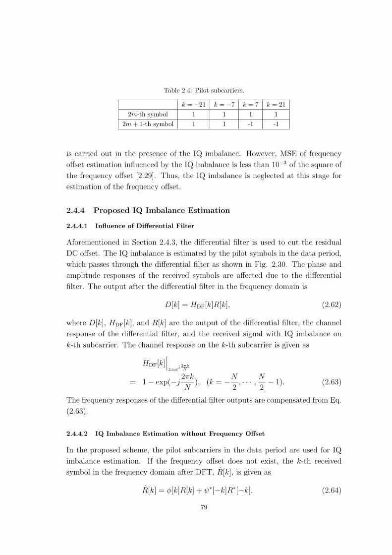
Table 2.4: Pilot subcarriers.
k = −21 k = −7 k = 7 k = 212m-th symbol 1 1 1 1
2m + 1-th symbol 1 1 -1 -1
is carried out in the presence of the IQ imbalance. However, MSE of frequency
offset estimation influenced by the IQ imbalance is less than 10−3 of the square of
the frequency offset [2.29]. Thus, the IQ imbalance is neglected at this stage for
estimation of the frequency offset.
2.4.4 Proposed IQ Imbalance Estimation
2.4.4.1 Influence of Differential Filter
Aforementioned in Section 2.4.3, the differential filter is used to cut the residual
DC offset. The IQ imbalance is estimated by the pilot symbols in the data period,
which passes through the differential filter as shown in Fig. 2.30. The phase and
amplitude responses of the received symbols are affected due to the differential
filter. The output after the differential filter in the frequency domain is
D[k] = HDF[k]R[k], (2.62)
where D[k], HDF[k], and R[k] are the output of the differential filter, the channel
response of the differential filter, and the received signal with IQ imbalance on
k-th subcarrier. The channel response on the k-th subcarrier is given as
HDF[k]∣∣∣z=ej 2πk
N
= 1 − exp(−j2πk
N), (k = −N
2, · · · ,
N
2− 1). (2.63)
The frequency responses of the differential filter outputs are compensated from Eq.
(2.63).
2.4.4.2 IQ Imbalance Estimation without Frequency Offset
In the proposed scheme, the pilot subcarriers in the data period are used for IQ
imbalance estimation. If the frequency offset does not exist, the k-th received
symbol in the frequency domain after DFT, R[k], is given as
R[k] = φ[k]R[k] + ψ∗[−k]R∗[−k], (2.64)
79

Figure 2.29: Vector representation of pilot subcarriers with IQ imbalance.
with
R[k] =
⎧⎨⎩S[k] k ∈ ND,
P [k] k ∈ NP,(2.65)
where S[k] is the k-th data subcarrier, P [k] is the k-th pilot subcarrier, ND is the
set of indices for the data subcarriers, and NP is the set of indices for the pilot
subcarriers. In Eq. (2.64),
φ[k] = φH[k], (2.66)
ψ[k] = ψH[k], (2.67)
and H[k] is the channel response of the k-th subcarrier. From Eq. (2.64), the
symbol on the k-th subcarrier OFDM symbol is affected by the the symbol on the
[−k]-th subcarrier due to the IQ imbalance. To estimate the IQ imbalance, the
pilot symbols shown in Table 2.4 are transmitted. The IQ imbalance is estimated
from the m-th and (m+1)-th consecutive OFDM symbols. Those two pilot symbols
are written as
Pm[k] = φ[k]Pm[k] + ψ∗[−k]P ∗m[−k], (2.68)
Pm+1[k] = φ[k]Pm+1[k] + ψ∗[−k]P ∗m+1[−k]. (2.69)
80

The mirror subcarriers of Eqs. (2.68) and (2.69) are also written as
Pm[−k] = φ[−k]Pm[−k] + ψ∗[k]P ∗m[k], (2.70)
Pm+1[−k] = φ[−k]Pm+1[−k] + ψ∗[k]P ∗m+1[k]. (2.71)
By substituting the values of the pilot symbols from Table 2.4 into Eqs. (2.68)-
(2.71) as shown in Fig. 2.29, φ and ψ are calculated as
ψ∗[−k] =Pm[k] + Pm+1[k]
2, (2.72)
φ[k] =Pm[k] − Pm+1[k]
2, (2.73)
φ[−k] =Pm[−k] + Pm+1[−k]
2, (2.74)
ψ∗[k] =Pm[−k] − Pm+1[−k]
2. (2.75)
From Eqs. (2.72) to (2.75), it is given as
ψ∗
φ∗ =ψ∗[−k] + ψ∗[k]
φ∗[k] + φ∗[−k], for k ∈ NP. (2.76)
From Eqs. (2.51) (2.52) and (2.76), β and θ are calculated. In the data period,
the received signal is compensated with the estimations of φ and ψ given in Eqs.
(2.37) and (2.38). The received symbol after IQ imbalance compensation, R[k], is
expressed as
R[k] =φ∗R[k] − ψ∗R[−k]
|φ|2 − |ψ|2 , for k ∈ ND ∪ NP. (2.77)
If the IQ imbalance is compensated completely, Eq. (2.77) is given as
R[k] = H[k]R[k], for k ∈ ND ∪ NP. (2.78)
The compensated symbol shown in Eq. (2.78) contains the channel response on
the k-th subcarrier. From the estimated channel response on each pilot subcarrier,
the channel response of the other subcarriers are compensated with the 1st order
interpolation.
2.4.4.3 IQ imbalance Estimation in the presence of Frequency Offset
In the time domain, the frequency offset causes additional phase rotation in the
data period. The frequency offset is estimated and compensated in the time domain
and IQ imbalance estimation is carried out in the frequency domain as shown
81

Figure 2.30: Receiver architecture of proposed scheme.
in Fig. 2.30. From Eq. (1.6), the n-th received signal after frequency offset
compensation in the time domain, r′[n], is expressed as
r′[n] = φr[n] + ψ∗r∗[n] exp(−j
2π(α + α)
Nn). (2.79)
The received symbol with the frequency offset in the frequency domain, R′[k], is
then given as
R′[k]
=N−1∑n=0
r′[n] exp(−j
2πl
Nn)
= φR[k] +ψ∗
N
(N−1∑n=0
R∗[−k] exp(−j2π(α + α)
Nn)
+N−1∑n=0
N2 −1∑
n=−N2
k′ �=−k
R∗[k′] exp(−j2π(k′ + k)
Nn) exp(−j
2π(α + α)
Nn)
).
(2.80)
From Eq. (2.80), it is shown that the ICI from all the subcarriers and the
closstalk from the symmetric subcarriers to the k-th subcarrier deteriorate the
accuracy of IQ imbalance estimation as shown in Fig. 2.31. Moreover, the aver-
82

Figure 2.31: Effect of ICI and frequency offset.
aging does not ignore the accuracy since the ICI components are affected by the
frequency offset.
2.4.5 Simulation Results
2.4.5.1 Simulation Conditions
The MSE of the IQ imbalance estimation is evaluated through computer simu-
lation. The simulation conditions are shown in Table 2.5. Information bits are
modulated with QPSK on each subcarrier. The number of DFT/IDFT points is
set to 64 while 52 subcarriers are used for the LTSP symbols, which follows the
IEEE 802.11a/g standard. The 1st order butterworth filter is employed as the Rx
HPF. The cutoff frequency of the received HPF is set to 10[kHz]. The DC offset
is set to 10[dB] [2.28]. The normalized frequency offset varies from 0.1 to 0.5. The
mismatch of amplitude is set to values from 0 to 0.1 and the mismatch of phase is
set to change from 0 to 10[degrees] [2.21].
2.4.5.2 Normalized MSE Performance vs. Frequency Offset
Figures 2.32 and 2.33 show the normalized MSE performance of gain and phase
mismatch estimation, respectively, when the frequency offset α is varied. The
phase mismatch β is set to 0.05 and the phase mismatch θ is set to 5[degrees].
Eb/N0 is set to {10, 15, or 20}[dB]. In those figures, ‘Conventional scheme’ refers
to the IQ imbalance estimation scheme in the time domain as shown in Section 2.3
[2.30]. It is clear that the proposed scheme is superior to the convetional scheme
when the frequency offset α is less than 0.2.
83

Table 2.5: Simulation conditions.
Trial number 10,000 timesModulation scheme QPSK+OFDM (Preamble)
64QAM+OFDM (Data)Number of subcarrier 64
Number of data Subcarrier 52Channel AWGNRx HPF 1st order Butterworth filter
fB=10[kHz]DC offset 10 [dB]
Normalized frequency offset 0.001-0.1Gain mismatch β 0.01-0.05Phase mismatch θ 1-5 [degrees]
Figure 2.32: Normalized MSE performance of gain mismatch estimation (β=0.05, θ=5[degrees]).
In both figures, the fluctuation in the MSE of the proposed scheme for different
frequency offset is due to the effect of the frequency offset in the second term of
the right side of Eq. (2.80). This tendency can be observed without ICI (R[k] =
0, for k ∈ ND) in the numerical results. This is because the frequency offset
rotates the phase of ψ∗ in the second term of Eq. (2.80).
From Eq. (2.50), with the assumption of small θ, β and θ depend on εI and εQ,
84

Figure 2.33: Normalized MSE performance of phase mismatch estimation (β=0.05, θ=5[degrees]).
respectively. To see the effect of the frequency offset, the real and imaginary parts
of the second term of Eq. (2.80) without the thermal noise are shown in in Figs.
2.34 and 2.35, respectively, when the frequency offset α is varied. In the figures,
‘Simulation’ indicates the numerical values obtained through computer simulation
and ‘Ideal’ means the value without frequency offset. The fluctuation of the real
part directly corresponds to the MSE of β estimation through Eqs. (2.49) and
(2.72) as indicated in Fig. 2.32. Also, the fluctuation of the imaginary part is
strongly related to the MSE of θ estimation through Eqs. (2.49) and (2.72) as
shown in Fig. 2.33.
2.4.5.3 Normalized MSE Performance vs. Gain Mismatch and Phase Mismatch
Figure 2.36 shows the normalized MSE performance of gain mismatch estimation
with the DC offset and the frequency offset when the gain mismatch value is varied.
The phase mismatch θ is set to 5[degrees] and the frequency offset α is set to 0.001.
Eb/N0 is set to {10, 15, or 20}[dB]. The MSE performance of the proposed scheme
is superior than the conventional scheme. It can be seen from Fig. 2.36 that the
normalized MSE performance improves as the gain mismatch increases. This is
because the MSE is normalized by the gain mismatch β. The normalized MSE of
the proposed scheme is reduced by a factor of about 10 − 100 as compared to the
conventional scheme.
85

Figure 2.34: Real part of the second term of Eq. (2.80) (SNR = ∞, β=0.05, θ=5[degrees]).
Figure 2.35: Imaginary part of the second term of Eq. (2.80) (SNR = ∞, β=0.05, θ=5[degrees]).
Figure 2.37 shows the normalized MSE performance of phase mismatch estima-
tion with the DC offset and the frequency offset when the phase mismatch value
is varied. The phase mismatch β is set to 0.05 and the frequency offset α is set to
86
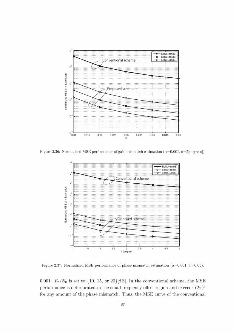
Figure 2.36: Normalized MSE performance of gain mismatch estimation (α=0.001, θ=5[degrees]).
Figure 2.37: Normalized MSE performance of phase mismatch estimation (α=0.001, β=0.05).
0.001. Eb/N0 is set to {10, 15, or 20}[dB]. In the conventional scheme, the MSE
performance is deteriorated in the small frequency offset region and exceeds (2π)2
for any amount of the phase mismatch. Thus, the MSE curve of the conventional
87

Figure 2.38: BER vs. normalized frequency offset α (64QAM, β=0.05, θ=5[degrees]).
scheme is set to (2π)2 and normalized, here. The MSE performance of the pro-
posed scheme is again superior than the conventional scheme. It can be seen from
Fig. 2.37 that the normalized MSE curves of both the proposed and conventional
schemes improve as the phase mismatch increases. This is because the MSE is nor-
malized by the phase mismatch θ. The normalized MSE of the proposed scheme
reduces by a factor of about 104 − 105 as compared with the conventional scheme.
2.4.5.4 BER Performance vs. Frequency Offset
Figure 2.38 shows the BER performance versus the frequency offset α. The gain
mismatch β is set to 0.05, the phase mismatch θ is set to 5 [degrees], and the
frequency offset α ranges from 0.001 to 0.3.
As shown in this figure, the BER curve for the conventional scheme decreases
as the frequency offset α increases. This is because IQ imbalance estimation does
not work well when the frequency offset is small as mentioned in Section 2.4.4
[2.30]. On the other hand, the BER curve of the proposed scheme is deteriorated
as the frequency offset α grows. This is again due to the ICI caused by the fre-
quency offset. From this figure, the proposed scheme exhibits superior estimation
performance as compared with the conventional scheme when the frequency offset
is small.
88

Figure 2.39: BER vs. Eb/N0 (64QAM, β=0.05, θ=5[degrees]).
2.4.5.5 BER Performance vs. Eb/N0
Figure 2.39 shows the BER performance in the presence of the frequency offset.
64QAM is used for data modulation. These plots are simulated using the 1st order
interpolation for phase compensation by pilot subcarriers. The gain mismatch
is β = 0.05, phase mismatch is θ = 5[degrees], and frequency offset α is set to
{0, 0.001, 0.01, or 0.05}. In this figure, ‘Conventional scheme’ refers to the IQ
imbalance estimation scheme in the time domain as shown in Section 2.4.4 [2.30].
‘No compensation’ represents the simulation in the case of no IQ imbalance and
frequency offset compensation, ‘THEORY’ is the theoretical BER curve for 64QAM
modulation.
As shown in Fig. 2.39, the BER curve of the conventional scheme actually
makes the BER worse because of inaccurate estimation of the IQ imbalance. The
proposed IQ imbalance estimation improves the BER performance. However, the
BER performance is deteriorated as the frequency offset α increases. This is be-
cause the estimated value in Eq. (2.80) suffers from the phase rotation due to the
frequency offset.
89
2.4.6 Conclusions
In this section, a low-complexity IQ imbalance estimation scheme in the presence
of the DC offset and the frequency offset has been proposed. The conventional
scheme uses the preamble signals in the time domain. However, the BER per-
formance is deteriorated when the frequency offset is small. In the proposed IQ
imbalance estimation scheme, the pilot subcarriers in the frequency domain are
employed. The numerical results obtained through computer simulation shows
that the proposed scheme works well when the frequency offset is small. The pro-
posed scheme improves the accuracy of estimation by a factor of 10 − 102 for the
gain mismatch and 104 − 105 for the phase mismatch with the small frequency
offset.
2.5 Conclusions of Chapter 2
In Chapter 2, the frequency offset and IQ imbalance estimation scheme in the
presence of time-varying DC offset for direct conversion receivers has been pro-
posed. In the proposed scheme, the key idea is to use a differential filter for the
reduction of the DC offset. The frequency offset and IQ imbalance are estimated
with simple calculation from the outputs of the differential filter in the presence
of the DC offset. Thus, the proposed low-complexity frequency offset and IQ im-
balance estimation schemes are suitable for low-cost and low-power-consumption
direct conversion receivers.
2.6 References
[2.1] W. Namgoong and T. H. Meng, “Direct-conversion RF Receiver Design,”
IEEE Trans. on Commun., vol.49, no.3, pp.518-529, March 2001.
[2.2] R. Svitek and S. Raman, “DC offsets in direct-conversion receivers: charac-
terization and implications,” IEEE Microwave Magazine, vol.6, no.3, pp.76-
86, Sept. 2005.
[2.3] D. Hui, B. Lidoff, and K. Zangi, “Enhanced DC Estimation via Sequence-
Specific Frequency Offset,” Proc. of the 56th IEEE Vehicular Technology
Conference, vol.1, pp.161-165, Sept. 2002.
[2.4] G. T. Gil, I. H. Sohn, Y. H. Lee, Y. I. Song, and J. K. Park, “Joint ML
Estimation of Carrier Frequency, Channel, I/Q Mismatch, and DC offset
90

in Communications Receivers,” IEEE Trans. on Vehi. Tech., vol.54, no.1,
pp.338-349, Jan. 2005.
[2.5] C. K. Ho, S.Sun, and P.He, “Low complexity frequency offset estimation
in the presence of DC offset,” Proc. of IEEE International Conference on
Communications, vol.3, pp.2051-2055, May 2003.
[2.6] T. Fujisawa, J. Hasegawa, K. Tsuchie, T. Shiozawa, T. Fujita, T. Saito,
and Y. Unekawa, “A Single-Chip 802.11a MAC/PHY With a 32-b RISC
Processor,” IEEE Journal of Solid-State Circuits, vol.38, no.11, pp.2001-
2009, Nov. 2003.
[2.7] H. Yoshida, T. Kato, T. Toyoda, I. Seto, R. Fujimoto, T. Kimura, O. Watan-
abe, T. Arai, T. Itakura, and H. Tsurumi, “Fully Differential Direct Conver-
sion Receiver for W-CDMA using an Active Harmonic Mixer,” Proc. of IEEE
Radio Frequency Integrated Circuit Symposium, pp.395-398, Jun. 2003.
[2.8] IEEE.802.11a-Part 11: Wireless LAN Medium Access Control (MAC) and
Physical Layer (PHY) specifications; Highspeed Physical Layer in the 5GHZ
Band.
[2.9] IEEE.802.11g-Part 11: Wireless LAN Medium Access Control (MAC) and
Physical Layer (PHY) specifications; Highspeed Physical Layer in the
2.4GHZ Band.
[2.10] W. Chen, T. Lee, and T. Lu, “A 5-GHz Direct Conversion Receiver with
I/Q Phase and Gain Error Calibration,” Proc. of IEEE Radio Frequency
Integrated Circuit Symposium, pp.201-204, Jun. 2005.
[2.11] R. G. Meyer, W. D. Mack, and J. Hageraats, “A 2.5 GHz BiCMOS
Transceiver for Wireless LAN,” Proc. of International Solid-State Circuits
Conference, pp.310-311, Feb 1997.
[2.12] S. Otaka, T. Yamaji, R. Fujimoto, and H. Tanimoto, “A Low Offset 1.9-GHz
Direct Conversion Receiver IC with Spurious Free Dynamic Range of over
67 dB,” IEICE Trans. on Fundamentals, vol.E84-A, no.2, pp.513-519, Feb.
2001.
[2.13] J. Olsson, “WLAN/WCDMA Dual-Mode Receiver Architecture Design
Trade-Offs,” Proc. of the 6th IEEE Circuits and Systems Symposium, vol.2,
pp.725-728, May 2004.
91

[2.14] M. Faulkner, “DC Offset and IM2 Removal in Direct Conversion,” IEE Proc.
Communications, vol.149, no.3, pp.179-184, June 2002.
[2.15] T. Liu and E. Westerwick, “5 GHz CMOS Radio Transceiver Front-end
Chipset,” Proc. of International Solid-State Circuits Conference, pp.320-321,
Feb. 2000.
[2.16] B. Razavi, “Design Considerations for Direct-Conversion Receivers,” IEEE
Trans. on Circuits and Systems II: Analog and Digital Signal Processing,
vol.44, no.6, pp.428-435, June 1997.
[2.17] A. A. Abidi, “Direct-Conversion Radio Transceivers for Digital Communi-
cations,” IEEE Journal of Solid-State Circuits, vol.30, no.12, pp.1399-1410,
Dec. 1995.
[2.18] R. B. Palipana and K. Chung, “The Effects of Receiver Impairments in
Terrestrial Digital Video Broadcasting,” Proc. of the 9th Asia-Pacific Con-
ference on Communications, vol.3, pp.1143-1146, Sept. 2003.
[2.19] M. Inamori, A. M. Bostamam, Y. Sanada, and H. Minami, “Frequency
Offset Compensation Scheme under DC Offset for OFDM Direct Conversion
Receivers,” Proc. of the 9th International Symposium on Wireless Personal
Multimedia Communications, pp.378-382, Sept. 2006.
[2.20] M. Inamori, A. M. Bostamam, Y. Sanada, and H. Minami, “Frequency Offset
Estimation Scheme in the Presence of Time-varying DC Offset for OFDM
Direct Conversion Receivers,” IEICE Trans. on Commun., vol.E90-B, no.10,
pp.2884-2890, Oct. 2007.
[2.21] J. Tubbax, A. Fort, L. V. Perre, S. Donnay, M. Moonen, and H. D. Man,
“Joint Compensation of IQ Imbalance and Frequency Offset in OFDM
Systems,” Proc. of IEEE Global Telecommunications Conference, vol.3,
pp.2365-2369, May 2003.
[2.22] D. S. Hilborn, S. P. Stapleton, and H. K. Cavers, “An Adaptive Direct
Conversion Transmitter,” IEEE Trans. on Veh. Tech., vol.43, no.2, pp.223-
233, May 1994.
[2.23] G. Xing, M. Shen, and H. Liu, “Frequency Offset and I/Q Imbalance Com-
pensation for Direct Conversion Receivers,” IEEE Trans. on Commun., vol.4,
pp.673-680, March 2005.
92
[2.24] S. D. Rore, E. L. Estraviz, F. Horlin, and L. V. Perre, “Joint Estimation
of Carrier Frequency Offset and IQ Imbalance for 4G Mobile Wireless Sys-
tems,” Proc. of IEEE International Conference on Communications, vol.5,
pp.2066-2071, June 2006.
[2.25] A. C. Douglas and S. Haykin, “On the Relationship Between Blind Deconvo-
lution and Blind Source Separation,” Proc. of the 31st Asilomar Conference
on Signals, Systems & Computers, vol.2, pp.1591-1595, Nov. 1997.
[2.26] M. Valkama, M. Renfors, and V. Koivunen, “Advanced Methods for I/Q
Imbalance Compensation in Communication Receivers,” IEEE Trans. Signal
Processing, vol.49, no.10, pp.2335-2344, Oct. 2001.
[2.27] P. Rykaczewski, J. Brakensiek, and F. Jondral, “Decision Directed Methods
of I/Q Imbalance Compensation in OFDM Systems,” Proc. of the IEEE
69th Vehicular Technology Conference-Fall, vol.1, pp.484-487, Sept. 2004.
[2.28] M. Inamori, A. M. Bostamam, Y. Sanada, and H. Minami, “Frequency Offset
Estimation Scheme in the Presence of Time-varying DC Offset for OFDM
Direct Conversion Receivers,” IEICE Trans. on Commun., vol.E90-B, no.10,
pp.2884-2890, Oct. 2007.
[2.29] M. Inamori, A. M. Bostamam, Y. Sanada, and H. Minami, “Frequency Offset
Estimation Scheme in the Presence of Time-varying DC Offset and IQ Im-
balance for OFDM Direct Conversion Receivers,” Proc. of the 18th Annual
International Symposium on Personal Indoor and Mobile Radio Communi-
cations, pp.1-5, Sept. 2007.
[2.30] M. Inamori, A. M. Bostamam, Y. Sanada, and H. Minami, “IQ Imbalance
Compensation Scheme in the Presence of Frequency Offset and Dynamic DC
Offset for a Direct Conversion Receiver,” IEEE Trans. on Wireless Commu-
nications, vol.8, no.5, pp.2214-2220, May 2009.
93


Chapter 3
Effect of Timing Jitter on
Quadrature Charge Sampling
This chapter evaluates the effect of timing jitter on quadrature charge sampling
for an RF-sampling receiver. In contrast to the voltage sampling, the charge
sampling mixer integrates the signal current instead of tracking the signal voltage.
The charge sampling mixer has been applied to RF direct sampling in wireless
receivers. The effect of timing jitter on charge sampling has been analyzed in
some literatures. However, in wireless receivers, quadrature sampling is required
in order to demodulate I-phase and Q-phase signals. Different from simple charge
sampling, timing jitter causes crosstalk between these signals. In this chapter, the
effect of timing jitter on quadrature sampling is investigated.
3.1 Introduction
RF front-end and ADCs are the key components of receiver architectures. If it
is possible to convert an RF signal directly to the digital samples, the analog
components of the receiver can be simplified. However, as there is no ADCs that
can be operated at RF, existing receivers cannot convert the received signal from
analog to digital domain directly [3.1].
Lately, new receiver architectures have been proposed [3.2]-[3.6]. These receivers
sample the received signal in RF. In these architectures, charge sampling mixers
are used, and sampling and downconversion are carried out simultaneously. The
baseband signal is then extracted through the discrete time analog filters.
The effect of timing jitter on charge sampling has been analyzed, for example, in
[3.7][3.8]. It has been shown that the effect of timing jitter on the SNR performance
of charge sampling is different from that of voltage sampling. If the timing jitter
95
is small, the SNR of charge sampling is worse than that of voltage sampling.
However, none of these literatures have assumed the application of the charge
sampling mixer to wireless receivers. In the wireless receiver, the received signal
consists of the I-phase and Q-phase components, which are sampled by quadrature
sampling [3.4][3.9]. The receiver may lose the orthogonality between the I-phase
and Q-phase components due to timing jitter and suffer from crosstalk between
them.
In this chapter, the effect of timing jitter on quadrature charge sampling for
an RF-sampling receiver is investigated. The signal-to-interference and noise ratio
(SINR) of the downconverted signal is evaluated with different data rates and
modulation schemes. In addition, this chapter models the distributions of timing
jitter based on the structure of the PLL. In the literature, such as in [3.7][3.8][3.10],
it is assumed that timing jitter can be modeled with a Gaussian distribution.
However, with a finite number of samples, the distribution of timing jitter has not
only a white noise component, but also a doubly integrated white noise component
(1/f2) [3.11][3.12]. It is also shown that the SINRs of charge sampling and voltage
sampling are almost equivalent when the jitter is sufficiently small.
This chapter is organized as follows. Section 3.2 gives the model of the phase
noise of the PLL. In Section 3.3, the effect of the phase noise on the received sig-
nal constellation is analyzed. Section 3.4 shows the numerical results obtained by
computer simulation. In this section, the phase noise is generated with random
numbers based on the model given in Section 3.2. The SNR and SINR of quadra-
ture charge sampling are presented, and the BER is simulated with AWGN. Section
3.5 gives our conclusions.
3.2 System Model
3.2.1 Receiver Architecture
The receiver architecture assumed in this chapter is shown in Fig. 3.1. In this
architecture, the received signal is sampled with the quadrature charge sampler.
The quadrature charge sampler samples the received signal at RF. The sampled
signals are then input into the finite impulse response (FIR) filters. Here, it is
assumed that all the coefficients of the FIR filters are set to 1 and they work as an
LPF. The LPF extracts the baseband aliasing component of the sampled signal.
Thus, with the charge sampler and the FIR filters, down conversion of the RF
signal can be achieved.
96

Figure 3.1: Block diagram of the receiver.
Figure 3.2: Simple integrating charge sampling circuit.
3.2.2 Charge Sampling Circuit
The simple circuit of the charge sampler is shown in Fig. 3.2 [3.7]. The input
voltage is first transformed into a corresponding current with a transconductance
element. For simplicity, it is assumed that this element performs ideal V-to-I con-
version. The output current of the transconductor is integrated into the sampling
capacitor during a predetermined period with the sampling switch Pint. After the
integration period, the output is sampled with the switch Pout, and the sampling
capacitor is discharged with the switch Pres before a new sample is taken.
3.2.3 PLL Model
The system model of the PLL is shown in Fig. 3.3. It is assumed that the output
signal is synchronized with that of the carrier signal for simplicity. This assump-
tion holds for a direct conversion receiver because the amount of phase rotation of
97

Figure 3.3: Block diagram of the PLL.
Figure 3.4: Typical PSD of the PLL phase noise.
the demodulated signal can be detected in the digital domain, and phase synchro-
nization may be achieved ideally with a digitally controlled oscillator [3.6].
The output from the PLL contains the phase noise whose spectrum has the
typical shape shown in Fig. 3.4. There are two major noise sources[3.11]. One is the
voltage-controlled oscillator (VCO), the other one is the temperature-compensated
crystal oscillator (TCXO) [3.12]. The phase noise caused by the TCXO is low-pass-
filtered by the transfer function of the PLL, and its power spectrum is concentrated
at around the carrier frequency. On the other hand, the power spectrum density
(PSD) of the phase noise caused by the VCO is much lower than that of the noise
caused by the TCXO at around the output frequency of the PLL. It can be seen
in Fig. 3.4 that the PSD value increases with frequency until it reaches a peak
and then decreases in proportion to the logarithm of frequency. It is the dominant
source of the phase noise if the frequency is far away from the output frequency.
For simplicity, it is assumed here that the PSD of the phase noise consists of two
components as shown in Fig. 3.5 [3.11]. One has a white spectrum shape with a
98

Figure 3.5: Modeled PSD of the PLL phase noise.
density of Ng. This component is dominant at frequency regions lower and higher
than the output frequency. The other one has a nonwhite spectrum shape with a
density of Nn at the output frequency. This PSD can be modeled by a single-pole
low-pass filter with a cutoff frequency of fB [3.12]. This component is dominant
around the output frequency.
3.3 Numerical Analysis
In this section, the effect of the phase noise modeled in Section 3.2 on signal
constellation with single carrier QAM and OFDM modulation is analyzed. The
SNR and SINR are then derived.
3.3.1 Single Carrier QAM
The transmitted signal is modulated with single carrier QAM and transmitted over
the AWGN channel. The received signal is given as
r(t) = s(t) + v(t)
= AI(t)mI cos(ωct) + AQ(t)mQ sin(ωct) + v(t), (3.1)
where AI and AQ are the amplitudes, and mI and mQ are the information signals
of the I-phase and Q-phase components, respectively.
The received RF signal is sampled as shown in Fig. 3.6. Here, the sampling
process is modeled by the multiplication of the received signal by the rectangular
signal and integration. It is also assumed that the phase of the rectangular signal
is synchronized with the received carrier signal. Each sampled signal of the I-phase
or Q-phase components is an integrated half cycle of the carrier signal as shown in
Fig. 3.7.
99
Figure 3.6: Quadrature sampling.
Here, the timing jitter on the I-phase or Q-phase signals is represented as τ [n].
The narrow-band Gaussian noise v(t) is given by
v(t) = vI(t) cos(ωct) + vQ(t) sin(ωct). (3.2)
When the symbol rate is fs, one symbol is transmitted from − 14fc
tofsfc
−1
fc+ 3
4fc.
The n-th sampled signal of the I-phase component rI [n] is then given by
rI [n] =1
Δ
∫ ( nfc
+Δ2
)+τ [n]
( nfc
−Δ2
)+τ [n]
{s(t) + v(t)} dt
= (AI [n]mI + vI [n])sinc(fcΔ) cos(ωcτ [n])
+(AQ[n]mQ + vQ[n])sinc(fcΔ) sin(ωcτ [n]), (3.3)
where Δ is the integration period, and AI [n], AQ[n], vI [n], and vQ[n] are given as
follows.
AI [n] =
∫ ( nfc
+Δ2
)+τ [n]
( nfc
−Δ2
)+τ [n]
AI(t) dt, (3.4)
AQ[n] =
∫ ( nfc
+Δ2
)+τ [n]
( nfc
−Δ2
)+τ [n]
AQ(t) dt, (3.5)
vI [n] =
∫ ( nfc
+Δ2
)+τ [n]
( nfc
−Δ2
)+τ [n]
vI(t) dt, (3.6)
vQ[n] =
∫ ( nfc
+Δ2
)+τ [n]
( nfc
−Δ2
)+τ [n]
vQ(t) dt. (3.7)
100

Figure 3.7: Sampling of the I-phase component.
ωcτ [n] is much less than the cycle of the carrier signal. The following approximation
can then be applied.
sin(ωcτ [n]) ≈ ωcτ [n], (3.8)
cos(ωcτ [n]) ≈ 1 − ωc2τ [n]2/2. (3.9)
From Eqs. (3.8) and (3.9), by setting Δ = 1/2fc, Equation (3.3) is approximated
as
rI [n] ≈ 2(AI [n]mI + vI [n])
π(1 − ωc
2τ [n]2
2) +
2(AQ[n]mQ + vQ[n])
π(ωcτ [n])
≈ 2(AI [n]mI + vI [n])
π+
2(AQ[n]mQ + vQ[n])
π(ωcτ [n]). (3.10)
The n-th sampled signal of the Q-phase component is also given as
rQ[n] =1
Δ
∫ ( nfc
+ 12fc
)+τ [n]
kfc
+τ [n]
{s(t) + v(t)} dt
≈ 2(AQ[n]mQ + vQ[n])
π− 2(AI [n]mI + vI [n])
π(ωcτ [n]). (3.11)
These sampled signals of the I-phase and Q-phase components are input into the
101

LPFs, respectively, the outputs of which are given by
dI =
fc/fs−1∑n=0
rI [n]
=
fc/fs−1∑n=0
2(AI [n]mI + vI [n])
π+
2(AQ[n]mQ + vQ[n])
π(ωcτ [n])
=2(AI [n]mI + vI)(fc/fs)
π+
2(AQ[n]mQ + vQ)(fc/fs)
π(ωcτ), (3.12)
dQ =
fc/fs−1∑n=0
rQ[n]
=
fc/fs−1∑n=0
2(AQmQ + vQ[n])
π− 2(AImI + vI [n])
π(ωcτ [n])
=2(AQmQ + vQ)(fc/fs)
π− 2(AImI + vI)(fc/fs)
π(ωcτ), (3.13)
where
τ =fs
fc
fc/fs−1∑n=0
τ [n], (3.14)
AI =fs
fc
fc/fs−1∑n=0
AI [n], (3.15)
AQ =fs
fc
fc/fs−1∑n=0
AQ[n], (3.16)
vI =fs
fc
fc/fs−1∑n=0
vI [n], (3.17)
vQ =fs
fc
fc/fs−1∑n=0
vQ[n]. (3.18)
Suppose that
G = 2(fc/fs)/π, (3.19)
Eqs. (3.12) and (3.13) become
dI = G{(AImI + vI) + (AQmQ + vQ)(ωcτ)}, (3.20)
dQ = G{(AQmQ + vQ) − (AImI + vI)(ωcτ)}, (3.21)
102

where vI and vQ are the white Gaussian noise with zero mean and a variance of
N0, respectively.
From Eq. (1.13), τ is given as
τ =fs
fc
fc/fs−1∑n=0
τ [n]
=fs
fc
fc/fs−1∑n=0
vp(ntc)
ωc
=fs
ωcfc
fc/fs−1∑n=0
vp(ntc)
=vp
ωc
. (3.22)
Thus, Eqs.(3.20) and (3.21) can be rewritten as
dI = G{(AImI + vI) + (AQmQ + vQ)(vp)}, (3.23)
dQ = G{(AQmQ + vQ) − (AImI + vI)(vp)}. (3.24)
From dI and dQ, the QAM symbol is demodulated.
3.3.2 OFDM Modulation
For the case of OFDM modulation, from Eqs.(3.23) and (3.24), the n-th sampled
signal of the I-phase or Q-phase component is rewritten as
dI [n] = G{(AImI [n] + vI [n]) + (AQmQ[n] + vQ[n])(vp)}, (3.25)
dQ[n] = G{(AQmQ[n] + vQ[n]) − (AImI [n] + vI [n])(vp)}, (3.26)
where
d[n] = dI [n] + jdQ[n]. (3.27)
Therefore, the demodulated signal on the k-th subcarrier can be written as
s[k] =1
N
N−1∑n=0
d[n] exp(j2πkn/N). (3.28)
3.3.3 SNR and SINR
As shown in Eqs. (3.3) and (3.9), timing jitter reduces the received signal am-
plitude from AI [n] to AI [n](1 − ω2cτ [n]2/2). From Eqs. (3.14) and (3.15), the
103

amplitude of the received I-phase signal is given as AI(1−ω2c τ
2/2). Therefore, the
SNR of the sampled I-phase component is calculated as [3.7][3.8]
SNR =(AI + vI)
2
(AI + vI)2(ω2c τ2
2)2
=4
ω4c τ
4. (3.29)
However, as shown in Eq. (3.3), for the case of quadrature sampling, there is a
crosstalk component from the Q-phase signal. Therefore, the SINR of the received
signal is calculated as
SINR =(AI + vI)
2
((AI + vI)ω2
c τ2
2)2 + ((AQ + vQ)ωcτ)2
.
(3.30)
3.3.4 Comparison of Charge Sampling and Voltage Sampling
From Fig. 3.7 and Eq. (3.3), the charge sampling of the I-phase component of
the carrier signal with the integration period of Δ and the timing jitter of τ [n] is
expressed as
1
Δ
∫ ∞
−∞rect
(t − ( nfc
+ τ [n])
Δ
)cos(ωct)dt
=1
Δ
∫ ( nfc
+Δ2
)+τ [n]
( nfc
−Δ2
)+τ [n]
cos(ωct)dt (3.31)
where rect(at) is the rectangular pulse shape with a width of a.
For charge sampling with the integration period of Δ, Eq. (3.31) is rewritten
as
1
Δωc
[sin(ωct)]nfc
+Δ2
+τ [n]
nfc
−Δ2
+τ [n]
=1
Δωc
(sin(2πk + πfcΔ + ωcτ [n]) − sin(2πk − πfcΔ + ωcτ [n]))
=2
Δωc
sin(πfcΔ) cos(ωcτ [n])
= sinc(fcΔ) cos(ωcτ [n]). (3.32)
104

The charge sampling of the Q-phase component is described as
∫ ( nfc
+Δ2
)+τ [n]
( nfc
−Δ2
)+τ [n]
sin(ωct)dt
=2
Δωc
sin(πfcΔ) sin(ωcτ [n])
= sinc(fcΔ) sin(ωcτ [n]). (3.33)
Then the SINR is given as in Eq. (3.30) with the condition of Δ = 1/2fc.
On the other hand, as Δ approaches 0, the rectangular pulse turns into Dirac’s
delta function. Voltage sampling is then expressed as follows:
limΔ→0
1
Δ
∫ ∞
−∞rect
(t − ( nfc
+ τ [n])
Δ
)r(t)dt
=
∫ ∞
−∞δ(t − (
n
fc
+ τ [n]))r(t)dt
= r( n
fc
+ τ [n]). (3.34)
The SINR of the voltage sampling is then given as [3.8]
Eˆr2`
nfc
´˜
Eˆ`
r`
nfc
+ τ [n]´ − r
`nfc
´´2˜
≈E
ˆr2`
nfc
´˜
Eˆr′2`
nfc
´τ2[n]
˜
=E
ˆ`AI
`nfc
´mI
`nfc
´+ nI
`nfc
´´2 cos2`ωc
nfc
´˜
Eˆ``−AI
`nfc
´mI
`nfc
´+ nI
`nfc
´´2 sin`ωc
nfc
´+
`AQ
`nfc
´mQ
`nfc
´+ nQ
`nfc
´´cos
`ωc
nfc
´´2ω2cτ2[n]
˜
=
`AI + vI
´2
`AQ + vQ
´2ω2c τ2
.
(3.35)
Comparing Eqs. (3.30) and (3.35), depending on the phase of the carrier signal, it
is clear that the SNR of voltage sampling can be much better than that of charge
sampling with small timing jitter. However, in terms of the SINR, there is no
significant difference between charge sampling and voltage sampling.
3.4 Numerical Results
3.4.1 Simulation Conditions
The effect of the modeled timing jitter on the received signal is evaluated by
computer simulation. The simulation conditions are shown in Table 3.1.
105

Table 3.1: Simulation conditions.
RF frequency 2.4 GHzNumber of simulated symbols 1,000,000 symbols
Modulation scheme QAM(QPSK, 16QAM, 64QAM)
OFDM(QPSK, 16QAM, 64QAM)
Number of subcarriers 64(OFDM)
Symbol rate fs 0.1,1,10,100[Msymbol/s]
Channel AWGNPSD of nonwhite phase noise Nn -80
Cutoff frequency fB 10 [kHz]PSD of white phase noise Ng -150∼-100 [dBc/Hz]
White noise components of the phase noise are assumed to have PSDs ranging
from −150 to −100 [dBc/Hz]. For example, the noise of the PLL proposed in
[3.13] shows a PSD of −110 [dBc/Hz]. The non-white noise component is modeled
by the single-pole low-pass filter with a cutoff frequency of 10 [kHz]. The PSD
of this component, Nn, is simulated with −80 [dBc/Hz] [3.13]. The simulation
is conducted with the symbol rates ranging from 0.1 to 100 [Msymbol/sec]. The
effects of the timing jitter on the SINR and BER performances are evaluated with
single carrier QAM and OFDM modulation.
3.4.2 SNR and SINR
Figures 3.8 and 3.9 show the SNR and SINR of the I-phase component defined in
Eqs. (3.29) and (3.30) as functions of the symbol rate. Eb/N0 is set to 14 [dB]. The
SNR and SINR show the same performance curves for both modulation schemes.
As the symbol rate decreases, both the SNR and SINR improve due to the noise
reduction capability of the FIR filter. The SNR remains unchanged among three
different modulation schemes, whereas the SINR largely depends on them. This is
due to the fact that the SINR is defined by the crosstalk term between the I-phase
and Q-phase components. With the same Eb/N0, the crosstalk term becomes larger
as the modulation index increases. Also, the SINR is significantly lower than the
SNR. Thus, instead of the SNR, the SINR should be calculated for quadrature
charge sampling in wireless receivers.
106

Figure 3.8: SNR and SINR versus symbol rate, (single carrier, Eb/N0 = 14 [dB]).
3.4.3 BER
The BER performance versus Eb/N0 with single carrier 64QAM is shown in Fig.
3.10. The symbol rate is 100 [Msymbol/s]. In this figure, when Ng is more than
-110 [dBc/Hz], the BER performance is worse than the theoretical performance.
This is due to the crosstalk component caused by the timing jitter in the quadrature
charge sampling mixers.
This result can be confirmed with a simple approximation. Assume that Ng
is -100 [dBc/Hz] and the symbol rate is 100 [Msymbol/s]. From Eq. (1.13),
E[(ωcτ [n])2] = −20 [dB], and from Eq. (3.30), the SINR of the sampled signal
is about 20 [dB]. When Eb/N0 = 14 [dB], i.e., Es/N0 = 22 [dB], the variance of
the thermal noise is almost the same as that of the interference. Thus, the BER
with the timing jitter and Eb/N0 = 14 [dB] should be the same as the theoretical
performance with Eb/N0 = 11 [dB], which is the result obtained in Fig. 3.10.
The BER performance versus the symbol rate with single carrier 64QAM is
shown in Fig. 3.4.3. Eb/N0 is set to 14 [dB]. As shown in this figure, as the symbol
rate increases, the BER increases. This is because the averaging effect of the FIR
filter decreases as the bandwidth increases.
107

Figure 3.9: SNR and SINR versus symbol rate, (OFDM, Eb/N0 = 14 [dB]).
Figure 3.10: BER versus Eb/No, (Ng =-100 [dBc/Hz], symbol rate=100 [Msymbol/s], singlecarrier 64QAM).
3.5 Conclusions of Chapter 3
In this chapter, the effect of timing jitter on quadrature charge sampling has been
derived and evaluated through computer simulation. Instead of the SNR, the
108

Figure 3.11: BER versus symbol rate (Ng = -100 [dBc/Hz], Eb/N0 = 14 [dB], single carrier64QAM).
SINR of the demodulated signal has been analyzed for wireless communication
applications. It has been shown that timing jitter deteriorates the SINR of the
demodulated signal due to crosstalk between the I-phase and Q-phase components
of the received signal. The BER performances with both single carrier QAM
and OFDM modulation schemes has shown the error floor with higher data rates.
Therefore, in a wideband system, the timing jitter in quadrature charge sampling
may limit the performance of the receiver. It has also been shown that the SINRs
of charge sampling and voltage sampling are almost the same, while the SNR of
voltage sampling is better than that of charge sampling.
3.6 References
[3.1] R. H. Walden, “Performance Trends for Analog-to-Digital Converters,”
IEEE Communications Magazine, vol.37, no.2, pp.96-101, Feb. 1999.
[3.2] J. Yuan, “A Charge Sampling Mixer with Embedded Filter Function for
Wireless Applications,” Proc. of the 2nd International Conference on Mi-
crowave and Millimeter Wave Technology, pp.315-318, Sept. 2000.
109

[3.3] S. Karvonen, T. Riley, and J. Kostamovaara, “Charge Sampling Mixer with
ΔΣ Quantized Impulse Response,” Proc. of International Symposium on
Circuits and Systems, vol.1, pp.129-132, May 2002.
[3.4] K. Muhammad, D. Leipold, B. Staszewski, Y. C. Ho, C. M. Hung, K. Mag-
gio, C. Fernando, T. Jung, J. Wallberg, J. S. Koh, S. John, I. Deng, O.
Moreira, R. Staszewski, R. Katz, and O. Friedman, “Discrete-Time Blue-
tooth Receiver in a 0.13μm Digital CMOS Process,” Proc. of International
Solid-State Circuits Conference, vol.1, pp.268-527, Feb. 2004.
[3.5] K. Muhammad and R. B. Staszewski, “Direct RF Sampling Mixer with
Recursive Filtering in Charge Domain,” Proc. of International Symposium
on Circuits and Systems, vol.1, pp.577-580, May 2004.
[3.6] R. B. Staszewski, K. Muhammad, D. Leipold, C. M. Hung, Y. C. Ho, J.
L. Wallberg, C. Fernando, K. Maggio, R. Staszewski, T. Jung, J. S. Koh,
S. John, D. I. Yuanying, V. Sarda, O. M. Tamayo, V. Mayega, R. Katz,
O. Friedman, O. E. Eliezer, E. Obaldia, and P. T. Balsara, “All-Digital
TX Frequency Synthesizer and Discrete-Time Receiver for Bluetooth Ra-
dio in 130-nm CMOS,” IEEE Journal of Solid-State Circuits, vol.39, no.12,
pp.2278-2291, Dec. 2004.
[3.7] S. Karvonen, T. Riley, and J. Kostamovaara, “On the Effects of Timing
Jitter in Charge Samping,” Proc. of International Symposium on Circuits
and Systems, vol.1, pp.737-740, May 2003.
[3.8] G. Xu and J. Yuan, “Performance Analysis of General Charge Sampling,”
IEEE Trans. on Circuts and Systems-II:Express Briefs, vol.52, no.2, pp.107-
111, Feb. 2005.
[3.9] S. Karvonen, T. A. D. Riley, and J. Kostamovaara, “A CMOS Quadrature
Charge-Domain Sampling Circuit with 66-dB SFDR up to 100HMz,” IEEE
Trans. on Circuits and Systems-I, vol.52, no.2, pp.105-117, March 2003.
[3.10] M. Shinagawa, Y. Akazawa, and T. Wakimoto, “Jitter Analysis of High-
Speed Sampling Systems,” IEEE Journal of Solid-State Circuits, vol.25,
no.1, pp.220-224, Feb. 1990.
[3.11] N. D. Dait, M. Harteneck, C. Sandner, and A. Wiesbauer, “Numerical Mod-
eling of PLL Jitter and the Impact of its Non-white Spectrum on the SNR of
Sampled Signals,” Proc. of Southwest Symposium on Mixed-Signal Design,
pp.38-44, Feb. 2001.
110

[3.12] N. D. Dalt, “Effect of Jitter on Asynchronous Sampling with Finite Number
of Samples,” IEEE Trans. on Circuits and Systems-II: Express Briefs, vol.51,
no.12, pp.660-664, Dec. 2004.
[3.13] R. B. Staszewski, C. Hung, D. Leipold, and P. T. Balsara, ”A First Multi-
gigahertz Digitally Controlled Oscillator for Wireless Applications,” IEEE
Trans. on Microwave Theory and Techniques, vol.51, no.11, pp.2154-2164,
Nov. 2003.
111


Chapter 4
Correlated Noise Cancellation
Scheme in Fractional Sampling
OFDM System
In this chapter, compensation schemes for signal distortion in FS OFDM receivers
are evaluated. The OFDM system with FS can achieve diversity with a single
antenna. In FS system, as the number of subcarriers and the oversampling ratio
increase, the correlation among the noise components over different subcarriers
deteriorates the BER performance. In Section 4.1, a correlated noise cancellation
scheme in FS OFCDM system is investigated. For applicability to OFDM systems,
the effect of the correlation among the noise components in FS OFDM system is
derived in Section 4.2. A metric weighting scheme for the coded FS OFDM system
is also proposed and investigated.
4.1 Fractional Sampling OFCDM with Alternative Spread-
ing Code
OFCDM has received large attention as a modulation scheme to realize high data
rate transmission. On the other hand, FS is a diversity scheme with a single
antenna, which achieves path diversity through oversampling and parallel signal
demodulation. In this section, the OFCDM system with FS is investigated. FS
causes correlation among noise components as the sampling rate is higher than
the Nyquist rate. This correlation may deteriorate the BER performance at the
receiver as the number of subcarriers and oversampling ratio increase. To over-
come this problem, correlated noise cancellation scheme in FS OFCDM system is
113

discussed in this section.
4.1.1 Introduction
OFCDM has received large attention as a modulation scheme to realize high data
rate transmission, which is based on code division multiple access (CDMA) [4.1]-
[4.3]. The OFCDM system transmits signals using more than 1000 subcarriers that
are orthogonally overlapped in the frequency domain.
On the other hand, various diversity schemes have been actively investigated
for the OFCDM-based system [4.4][4.5]. One of the typical diversity schemes is
antenna diversity in which multiple antenna elements are implemented in the re-
ceiver [4.4]. However, it may be difficult to implement multiple antenna elements
in small devices. Therefore, a new diversity scheme called FS has been proposed
in [4.6]. This scheme tries to acquire diversity gain through the signal sampled
faster than the Nyquist rate in the receiver. FS is known to covert a single-input
single-output (SISO) channel into a single-input multiple-output (SIMO) channel.
In [4.6], subcarrier-based noise whitening and MRC have been investigated because
of their low complexity. However, as the number of subcarriers and the oversam-
pling ratio increase, the correlation among the noise components over different
subcarriers deteriorates the BER performance.
To solve this problem, an OFCDM system with the alternative spreading code
is investigated. This spreading code has positive and negative components alter-
natively. Therefore, the OFCDM system with the alternative spreading code can
cancel the correlated noise components. The performance of the FS OFCDM sys-
tem with the alternative spreading code is evaluated through computer simulation
in this section.
Firstly, a system model is described briefly in subsection 4.1.2. The signal
processing of the proposed scheme for the FS OFCDM system is then discussed
in subsection 4.1.3. Numerical results are shown in subsection 4.1.4. Finally,
conclusions are presented in subsection 4.1.5.
4.1.2 System Model
4.1.2.1 Transmitter Model
Figure 4.1 shows the block diagram of an OFCDM transmitter [4.1][4.2]. The input
data is modulated with QPSK and is serial-to-parallel (S/P) converted to N/Sf
parallel sequences, where N denotes the number of subcarriers and Sf denotes the
spreading factor in the frequency domain. Each modulated symbol is duplicated
114

Figure 4.1: OFCDM transmitter block diagram.
Figure 4.2: Receiver block diagram.
into Sf parallel copies. Each branch of the symbol stream is then multiplied by a
chip from the spreading code with the repetition period of Sf , which is represented
as
s[(x − 1)Sf + i] = d[x]qi,
1 ≤ x ≤ N/Sf , 0 ≤ i≤Sf − 1, (4.1)
where s[(x − 1)Sf + i] is the i-th spread data component of the x-th data symbol
transmitted over the [(x − 1)Sf ]-th subcarrier, and d[x] is the x-th data symbol,
and qi is the i-th spreading code. The spread data sequence is modulated to the
multi-carrier signal by IDFT, and the GI is inserted to the modulated signal.
4.1.2.2 Receiver Structure with Fractional Sampling
At the receiver side, FS and MRC are used to achieve diversity over a multipath
channel [4.6]. The block diagram of an OFCDM receiver with FS is shown in Fig.
115

Figure 4.3: Correlation of the noise components (logarithmic representation of absolute value).
4.2. The received signal is downconverted to baseband and fractionally sampled.
The sampled signals are separated to G branches. The GI is removed on each of
the branches. The samples are serial-parallel converted and put into DFT. The
outputs of the DFT are then parallel-to-serial (P/S) converted. The signals on
all G branches are put into the whitening filter as the noise components of the
fractionally sampled signals are correlated. The output of the whitening filter are
then combined together as mentioned in subsection 1.4.3. The combined signal is
despread and demodulated, which is represented as
d[x] =
Sf−1∑i=0
s[(x − 1)Sf + i]qi. (4.2)
In FS system, the received signal is sampled at a rate higher than the Nyquist
rate in order to acquire the diversity gain. As the sampling rate G increases, G
OFDM demodulators are required. The computational complexity is increased by
a factor G as compared to usual OFDM system. In addition, the covariance matrix
is required for noise whitening.
4.1.3 Proposed Scheme
4.1.3.1 Despreading with Non-alternative Spreading Code
Suppose that the spreading code with the following condition is employed.
qi = qi+1 = · · · = qi+Sf−1. (4.3)
116

From Eq. (1.42) in Chapter 1, the correlated noise after despreading from the
k-th to the (k + Sf − 1)-th subcarriers, γnon[k, k + Sf − 1], is expressed as
γnon[k, k + Sf − 1]
=
Sf+k−1∑k1=k
(G−1∑g1=0
N−1∑k2=0k2 �=k1
G−1∑g2=0
H ′g1
[k1][Rn[k1, k2]]g1,g2ωg2 [k2])
=G−1∑g1=0
N−1∑k2=0k2 �=k1
G−1∑g2=0
(H ′g1
[k][Rn[k, k2]]g1,g2
+H ′g1
[k + 1][Rn[k + 1, k2]]g1,g2 + · · · +H ′
g1[k + Sf − 1][Rn[k + Sf − 1, k2]]g1,g2)ωg2 [k2].
(4.4)
The correlation among the noise components, R12w, over the subcarriers and over-
sampling indexes (k1G + g1 ≤ 100, k2G + g2 ≤ 100) is shown in Fig. 4.3, where
the non-diagonal elements of this matrix are almost periodic over the neighboring
indexes. Moreover, from Eq. (1.36), if the number of subcarriers increases and
the spreading factor is small enough, the following approximation on the noise
covariance matrices can be assumed.
R− 1
2w [k] ≈ R
− 12
w [k + 1] ≈ · · · ≈ R− 1
2w [k + Sf − 1]. (4.5)
Thus, from Eqs. (4.5),
[Rn[k, k2]]g1,g2 ≈ [Rn[k + 1, k2]]g1,g2
≈ · · · ≈ [Rn[k + Sf − 1, k2]]g1,g2 . (4.6)
If the correlation of the channel responses of the subcarriers is high, the following
approximation is also derived.
H ′g1
[k] ≈ H ′g1
[k + 1] ≈ · · · ≈ H ′g1
[k + Sf + 1]. (4.7)
From Eqs. (4.6) and (4.7), the correlated noise after despreading can be approxi-
mated as follows.
γnon[k, k + Sf − 1]
≈G−1∑g1=0
N−1∑k2=0k2 �=k1
G−1∑g2=0
Sf (H′g1
[k][Rn[k, k2]]g1,g2)ωg2 [k2].
(4.8)
117

If the size of the matrix and the spreading factor increases, the total amount of
the correlated noise in Eq. (1.42) grows. Therefore, the BER performance is
deteriorated with the correlated noise component.
4.1.3.2 Despreading with Alternative Spreading Code
If the number of the subcarriers and the oversampling ratio increase, the total
amount of the correlated noise in Eq. (1.42) grows. To solve this problem, a
spreading code which has the following property is used.
q2i = −q2i+1, i = 0, 1, · · · , Sf/2 − 1. (4.9)
This code is referred to as the alternative spreading code in this section. From
Eqs. (1.27) and (4.6), the correlated noise is approximated as
γalt[k, k + Sf − 1]
=
Sf+k∑k1=k
G−1∑g1=0
N−1∑k2=0k2 �=k1
G−1∑g2=0
q(k1−k)H′g1
[k1] · [Rn[k1, k2]]g1,g2ωg2 [k2].
(4.10)
From Eqs. (4.7), (4.9), and (4.10), the correlated noise after despreading from the
k-th to (k + Sf − 1)-th subcarriers, γalt, is given as
γalt[k, k + Sf − 1]
≈Sf+k∑k1=k
G−1∑g1=0
H ′g1
[k] ·N−1∑k2=0k2 �=k1
(−1)(k−k1){G−1∑g2=0
[Rn[k1, k2]]g1,g2ωg2 [k2]}.
(4.11)
The inside of the braces in Eq. (4.11) cancels between the k1-th and (k1 + 1)-th
subcarriers because of the element, (−1)(k−k1). This element is based on the prop-
erty of the alternative spreading code given in Eq. (4.9) Thus, despreading with
the alternative spreading code cancels most of the correlated noise components.
However, the drawback of this scheme is that the number of available spreading
codes reduces to half. This is also due to the constraint shown in Eq. (4.9).
4.1.4 Numerical Results
4.1.4.1 Simulation Conditions
The FS OFCDM system with the alternative spreading code is evaluated through
computer simulation. Simulation conditions are shown in Table 4.1, which assume
118

Table 4.1: Simulation conditions.
Bandwidth 80MHzNumber of subcarriers 256/512/1024
Guard Interval 12.8/25.6/51.2[μsec]Subcarrier spacing Δf 78.1/39.1/19.5 [kHz]Number of IDFT points 256/512/1024DFT sampling speed Ts 12.5 [nsec]
Data modulation QPSKChannel estimation Ideal
Fractional sampling ratio G 1,2,4Spreading factor Sf 2/4/8/16
Channel model Rayleigh fading16 path uniform/24 path exponential
the 4G system is assumed. The data is modulated with QPSK. The received signal
is sampled at the rates of 1/Ts, 2/Ts, and 4/Ts. The spreading factor, Sf , is set
from 2 to 16 in this simulation. Channel estimation is assumed to be ideal. Here,
two channel models are considered. One is a 16 path Rayleigh fading model with
a uniformed delay profile as shown in Fig. 4.5(a) [4.6]. The interval between the
path delays in this model is Ts/4. The other one is a 24 path Rayleigh fading
model with an exponential delay profile as shown in Fig. 4.5(b) [4.2]. The interval
between the path delays is 5Ts. The composite impulse response of the transmit
and receive pulse shaping filters is assumed to be a sinc pulse with a duration of
2Ts [4.6]. Fig. 4.4 shows the frequency response of the pulse shaping filters with
the impulse response of the rectangular pulse and the truncated sinc pulse. If the
rectangular pulse is applied, the non-diagonal elements of R1/2w equal to 0, which
means no correlated noise components. Therefore, the BER performance with the
rectangular pulse is equivalent to that of a SIMO model [4.7].
4.1.4.2 BER Improvement with Alternative Spreading Code
Figures 4.6 and 4.7 show the BER performance of the 16 and 24 path Rayleigh
fading channel models, respectively. The number of subcarriers is 1024 and the
spreading factor is 2. Numerical results of the 1×4 SIMO model are shown in the
same figure as a reference. This SIMO model is assumed to receive uncorrelated
signals at each antenna.
From these figures, when the oversampling ratio is 1 or 2, the BERs with both
alternative and non-alternative spreading codes are almost the same. On the other
119

Figure 4.4: PSD vs. normalized frequency with different pulse shapes.
hand, if the oversampling ratio is 4, the BER with the non-alternative spreading
code is larger than that with the oversampling ratio of 2. This is due to the
correlated noise components in Eq. (1.42). On the contrary, the BER with the
alternative spreading code reduces as the oversampling ratio increases. This is
because the alternative spreading code cancels the correlated noise components
among the adjacent subcarriers as shown in Eq. (4.11). In Fig. 4.7, the improve-
ment on the BER curve is limited in comparison with Fig. 4.6. The reason is
that the delay spread assumed in the exponentially decay model is larger. There-
fore, the fluctuation on the channel responses among the adjacent subcarriers is
larger and the approximation in Eq. (4.7) becomes inaccurate. Thus, the residual
component of the correlated noise after despreading limits the improvement of the
BER performance.
4.1.4.3 Number of Subcarriers
In Figs. 4.8 and 4.9, the relationship between the BER and the number of subcar-
riers for both alternative and non-alternative spreading codes is presented. Here,
Eb/N0 is set to 15[dB], the spreading factor is set to 2, and the oversampling ratio
is set to G = {1, 2, 4}. In Fig. 4.9, the BERs are deteriorated when the number
120

(a) 16 path Rayleigh fading model with uniform delay spread.
(b) 24 path Rayleigh fading model with exponential delay spread.
Figure 4.5: Multipath channel models.
of subcarriers is 256. This is because the delay spread is large on the 24 path
Rayleigh fading channel and some of the paths have larger delays than the GI.
When the number of subcarriers is more than 512, the largest delay of the paths
is accommodated within the GI. In both figures, the BERs of G = {1, 2} remain
fairly constant. As the number of subcarriers increases, the BER with the non-
alternative spreading code increases when G = 4 and the number of subcarriers
is 1024. This is because of the correlated noise components between the adjacent
subcarriers. The reason is that the value of the element in Rn[k, j] in Eq. (1.41)
is of the order of 10−4 and the total amount of the correlated noise components
becomes close to that of the white noise.
4.1.4.4 Spreading Factor Sf
In Figs. 4.10 and 4.11, the relationship between the BER and the spreading fac-
tor for both alternative and non-alternative spreading codes on different channel
models is presented. Here, Eb/N0 is set to 15[dB] and the oversampling ratio is
set to G = {1, 2, 4}. The number of subcarriers is 1024. In Fig. 4.10, the BERs
with G = {1, 2} remain fairly constant. As the spreading factor increases, the
121

Figure 4.6: BER performance vs. Eb/N0 on the 16 path Rayleigh fading channel with the uniformdelay profile (number of subcarriers: 1024, Sf=2).
Table 4.2: Spreading code.
1st low 1 1 1 1 1 1 1 1 1 1 1 1 1 1 1 12nd low 1 -1 1 -1 1 -1 1 -1 1 -1 1 -1 1 -1 1 -13rd low 1 1 -1 -1 1 1 -1 -1 1 1 -1 -1 1 1 -1 -15th low 1 1 1 1 -1 -1 -1 -1 1 1 1 1 -1 -1 -1 -19th low 1 1 1 1 1 1 1 1 -1 -1 -1 -1 -1 -1 -1 -1
BER with the alternative spreading code decreases when G = 4. This is due to
the effect of frequency diversity. In contrast, when G = 4, the BER with the non-
alternative spreading code is deteriorated as the spreading factor increases. The
reason behind is the correlated noise given in Eq. (4.8). If the spreading factor,
Sf , increases, the variance of the noise also grows with the factor of Sf2. As for
the results corresponding to the alternative spreading code, the BER is improved
as the spreading factor increases. This is because the alternative spreading code
can cancel the correlated noise. More diversity gain is obtained with the proposed
spreading code in Fig. 4.11. This is due to the assumed channel model. Since the
delay spread assumed in the exponential delay model is larger than that in the uni-
form decay model, the correlation among the channel responses of the subcarriers
122

Figure 4.7: BER performance vs. Eb/N0 on the 24 path Rayleigh fading channel with theexponential delay profile (number of subcarriers: 1024, Sf=2).
is smaller in Fig. 4.11.
4.1.4.5 Spreading Code
In order to show the validity of the alternative spreading code, the relationship
between the BER and G for various spreading codes on the two different channel
models is presented in Figs. 4.12 and 4.13. Here, Eb/N0 is set to 15[dB] and the
number of subcarriers is 1024. The 1st, 2nd, 3rd, 5th, and 9th rows of the Walsh-
Hadamard matrix with the size of 16 are used as the spreading codes [4.2]. Table
4.2 shows the spreading code used in this simulation. The 2nd row corresponds
to the proposed alternative spreading code. Both Figs. 4.12 and 4.13 show that
BERs with G = {1, 2} are almost the same for all spreading codes. Moreover, the
figures also show that the alternative spreading code gives the best result when
G = 4 while the worst result is given by the 1st row (non-alternative spreading
code). The results with the other codes (3rd, 5th, 9th) are spread between them.
The reason is that the pair of the blocks of “1” and “-1” in the spreading code
cancels the correlated noise components if the channel responses corresponding to
those blocks are sufficiently close. As the size of the block reduces, the difference
between the corresponding channel responses in those blocks decreases and the
123
Figure 4.8: BER performance vs. number of subcarriers on the 16 path Rayleigh fading channelwith the uniform delay profile (Sf = 2, Eb/N0 = 15[dB]).
residual of the correlated noise components diminishes.
4.1.5 Conclusions
The FS OFCDM system with the alternative spreading code has been investigated
in this section. In the FS OFCDM system, the correlation between the noise
components may deteriorate the BER performance at the receiver with the increase
of the number of subcarriers and oversampling ratio. The proposed spreading
code mitigates the effect of the correlated noise components and improves the
BER performance, especially when the oversampling rate is 4. It has also been
shown that the FS OFCDM system with the alternative spreading code can obtain
frequency diversity effect.
4.2 Effect of Pulse Shaping Filters on a Fractional Sam-
pling OFDM System with Subcarrier-Based Maximal
Ratio Combining
In this section, the effect of the impulse response of pulse shaping filters on a FS
OFDM system is investigated. FS achieves path diversity with a single antenna
124

Figure 4.9: BER performance vs. number of subcarriers on the 24 path Rayleigh fading channelwith the exponential delay profile (Sf = 2, Eb/N0 = 15[dB]).
Figure 4.10: BER performance vs. spreading factor Sf on the 16 path Rayleigh fading channelwith the uniform delay profile (number of subcarriers:1024, Eb/N0 = 15[dB]).
125

Figure 4.11: BER performance vs. spreading factor Sf on the 24 path Rayleigh fading channelwith the exponential delay profile (number of subcarriers:1024, Eb/N0 = 15[dB]).
Figure 4.12: BER performance vs. G with different spreading codes on the 16 path Rayleighfading channel with the uniform delay profile (number of subcarriers:1024, Eb/N0 = 15[dB]).
126
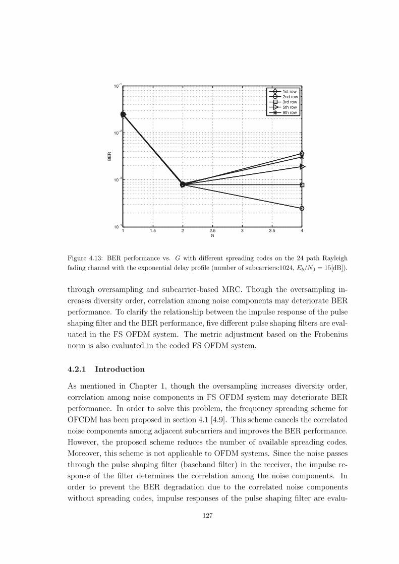
Figure 4.13: BER performance vs. G with different spreading codes on the 24 path Rayleighfading channel with the exponential delay profile (number of subcarriers:1024, Eb/N0 = 15[dB]).
through oversampling and subcarrier-based MRC. Though the oversampling in-
creases diversity order, correlation among noise components may deteriorate BER
performance. To clarify the relationship between the impulse response of the pulse
shaping filter and the BER performance, five different pulse shaping filters are eval-
uated in the FS OFDM system. The metric adjustment based on the Frobenius
norm is also evaluated in the coded FS OFDM system.
4.2.1 Introduction
As mentioned in Chapter 1, though the oversampling increases diversity order,
correlation among noise components in FS OFDM system may deteriorate BER
performance. In order to solve this problem, the frequency spreading scheme for
OFCDM has been proposed in section 4.1 [4.9]. This scheme cancels the correlated
noise components among adjacent subcarriers and improves the BER performance.
However, the proposed scheme reduces the number of available spreading codes.
Moreover, this scheme is not applicable to OFDM systems. Since the noise passes
through the pulse shaping filter (baseband filter) in the receiver, the impulse re-
sponse of the filter determines the correlation among the noise components. In
order to prevent the BER degradation due to the correlated noise components
without spreading codes, impulse responses of the pulse shaping filter are evalu-
127

Figure 4.14: Block diagram of a receiver.
ated for the FS OFDM system in this section. The effect of the impulse response
of the filter on the BER performance is then clarified.
This section is organized as follows. Firstly, a system model is described briefly
in subsection 4.2.2. The correlation among the noise components is then discussed
in subsection 4.2.3. Numerical results are shown in subsection 4.2.4. Finally,
conclusions are presented in subsection 4.2.5.
4.2.2 Receiver Structure with Fractional Sampling
At the receiver side, FS and MRC are used to achieve diversity over a multipath
channel [4.6]. The block diagram of an OFDM receiver with FS is shown in Fig.
4.14.
4.2.3 Noise Correlation among Samples
As mentioned in Chapter 1, the second term of the right side of Eq. (1.42) gives
the correlation between the noise components after subcarrier based noise whiten-
ing. These components may deteriorate the BER performance of the receiver. The
correlation among the noise components is determined by the impulse response of
the filter because the noise passes through the pulse shaping filter. An example of
the correlation among the noise components, R12w, over the subcarriers and over-
sampling indexes (k1G + g1 ≤ 100, k2G + g2 ≤ 100) is shown in Fig. 4.15. A
sinc pulse is assume as the impulse response of the pulse shaping filter. From Eq.
(1.36), this is the function of the impulse response of the pulse shaping filter in
the receiver. In order to improve the BER performance, the Frobenius norm of
Rn[k1, k2] should be kept small. Here, the Frobenius norm of a matrix A is given
128

Figure 4.15: Correlation of the noise components (logarithm representation of absolute value).
as
||A||F =
√√√√G−1∑g1=0
G−1∑g2=0
([A]g1,g2)2 (4.12)
where || · ||F denotes the Frobenius norm [4.10].
From Eq. (1.41), Rn[k1, k2] is given as follows.
Rn[k1, k2] = R− 1
2w [k1]R
12w[k1, k2], (4.13)
where R12w[k1, k2] is the (k1, k2)-th subblock of R
12w. The distribution of the eigen-
values for particular types of matrices has been investigated, especially for MIMO
transmission [4.11][4.12]. However, the distribution is not given for general ma-
tricies. Since R12w[k1, k2] does not have a specific matrix structure, the eigenvalues
of R12w[k1, k2] are not able to be analysed. On the other hand, since R
12w[k1] is a
Hermitian matrix and positive semidefinite, the Frobenius norm of the whitening
matrix, R− 1
2w [k1], is given by
||R− 12
w [k1]||2F =G−1∑g=0
(1/λg[k1])2, (4.14)
where λg[k1] is the g-th eigenvalue of R12w[k1] [4.10]. Also, ||Rw[k1]||2F =
∑G−1g=0 (λg[k1])
4.
129
Table 4.3: Simulation conditions
Bandwidth 80MHzNumber of data subcarriers 48/768
Guard interval 0.2/3.2[μsec]Subcarrier spacing Δf 1250/78.1 [kHz]Number of IDFT points 64/1024DFT sampling speed Ts 12.5 [nsec]
Data modulation QPSK, 16QAM, 64QAM/OFDMChannel estimation Ideal
Fractional sampling ratio G 1,2,4Channel model Rayleigh fading
(16path uniform/24path exponential)GSM Typical urban model
Channel coding Convolutional code(R = 1/2, K = 7)
Channel decoding Soft decision Viterbi decoder
From Eq. (1.36), the (g1, g2)-th element of Rw[k1] is given as
[Rw[k1]]g1,g2
= σ2v
1
N
N−1∑nd=−N+1
(N − |nd|)p2((nd + (g2 − g1)/G)Ts)
× e−j2πknd
N . (4.15)
From Eqs. (4.12), (4.14) and (4.15), the inverse of the Frobenius norm of R− 1
2w [k1]
is related to the specturm of the composite response, p2(t), because of the term,
p2((nd + (g2 − g1)/G)Ts)e−j
2πkndN , which is the same as the one in the discrete
Fourier transform. Therefore, in this section, the Frobenius norm of the whitening
matrix for five different impulse responses of the pulse shaping filter is investigated
through computer simulation.
4.2.4 Numerical Results
4.2.4.1 Simulation Conditions
Simulation conditions are shown in Table 4.3, which assumes the 4G system.
The data is modulated with QPSK, 16QAM, and 64QAM, and multiplexed with
OFDM. The bandwidth of the OFDM system is 80MHz. The DFT size is 64 and
1024 while the number of data subcarriers is 48 and 768. The received signal is
130

Table 4.4: 6-ray GSM Typical Urban model parameters.
Tap Relative Average relative Delaynumber time (μs) power (dB) in samples
1 0.0 -3.0 02 0.2 0.0 33 0.5 -2.0 84 1.6 -6.0 255 2.3 -8.0 356 5.0 -10.0 77
Figure 4.16: 6-ray GSM Typical Urban model.
sampled at the rates of 1/Ts, 2/Ts, and 4/Ts (G = 1, 2, 4). As channel coding, a
convolutional code with a coding rate of 1/2 is used. Soft decision Viterbi decoding
is employed in the receiver.
4.2.4.2 Channel Models
In this section, three channel models are assumed in the simulation. One is 6-ray
GSM Typical Urban model. The 6-ray GSM Typical Urban model is one of the
propagation models that are mentioned in the main body of 3GPP TS 45.005. The
parameters of the 6-ray GSM Typical Urban model is defined in Table 4.4. Fig.
4.16 shows the delay profile of 6-ray GSM Typical Urban model. The amplitude
of the path follows Rayleigh distribution. The others are Rayleigh fading channel
models. A 16 path Rayleigh fading model with an uniformed delay profile is shown
in Fig. 4.17(a) [4.6]. The interval between the path delays in this model is Ts/4. A
24 path Rayleigh fading model with an exponential delay profile is shown in Fig.
4.17(b) [4.2]. The interval between the path delays is 5Ts. The channel response
is assumed to be constant during one OFDM symbol interval. The GSM model
131

(a) 16 path Rayleigh fading model with uniform delay spread.
(b) 24 path Rayleigh fading model with exponential delay spread.
Figure 4.17: Multipath Rayleigh fading channel models.
and 24 path Rayleigh fading model are applied to the OFDM system with 1024
subcarriers.
132

(a) Impulse responses of the pulse shaping filter.
(b) Frequency spectrums of the pulse shaping filter.
Figure 4.18: Graphical illustration of the pulse shaping filters.
4.2.4.3 Pulse Shaping Filters
To clarify the effect of the spectrum of the filter on the BER performance, the
pulse shaping filter with the following 5 different impulse responses are employed
both at the transmitter and the receiver [4.6][4.13]. These impulse responses have
different bandwidths and are classified into two different types of sinc-based and
cosine-based pulse shaping filters [4.14].
133
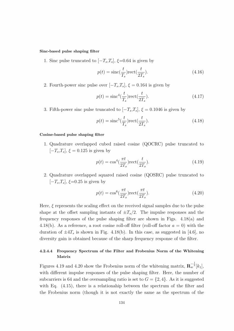
Sinc-based pulse shaping filter
1. Sinc pulse truncated to [−Ts,Ts], ξ=0.64 is given by
p(t) = sinc(t
Ts
)rect(t
2Ts
). (4.16)
2. Fourth-power sinc pulse over [−Ts,Ts], ξ = 0.164 is given by
p(t) = sinc4(t
Ts
)rect(t
2Ts
). (4.17)
3. Fifth-power sinc pulse truncated to [−Ts,Ts], ξ = 0.1046 is given by
p(t) = sinc5(t
Ts
)rect(t
2Ts
). (4.18)
Cosine-based pulse shaping filter
1. Quadrature overlapped cubed raised cosine (QOCRC) pulse truncated to
[−Ts,Ts], ξ = 0.125 is given by
p(t) = cos4(πt
2Ts
)rect(t
2Ts
). (4.19)
2. Quadrature overlapped squared raised cosine (QOSRC) pulse truncated to
[−Ts,Ts], ξ=0.25 is given by
p(t) = cos6(πt
2Ts
)rect(πt
2Ts
). (4.20)
Here, ξ represents the scaling effect on the received signal samples due to the pulse
shape at the offset sampling instants of ±Ts/2. The impulse responses and the
frequency responses of the pulse shaping filter are shown in Figs. 4.18(a) and
4.18(b). As a reference, a root cosine roll-off filter (roll-off factor a = 0) with the
duration of ±4Ts is shown in Fig. 4.18(b). In this case, as suggested in [4.6], no
diversity gain is obtained because of the sharp frequency response of the filter.
4.2.4.4 Frequency Spectrum of the Filter and Frobenius Norm of the WhiteningMatrix
Figures 4.19 and 4.20 show the Frobenius norm of the whitening matrix, R− 1
2w [k1],
with different impulse responses of the pulse shaping filter. Here, the number of
subcarriers is 64 and the oversampling ratio is set to G = {2, 4}. As it is suggested
with Eq. (4.15), there is a relationahip between the spectrum of the filter and
the Frobenius norm (though it is not exactly the same as the spectrum of the
134

Figure 4.19: Frobenius norm of the whitening filter for different impulse responses (Number ofsubcarriers=64, G = 2).
Figure 4.20: Frobenius norm of the whitening filter for different impulse responses (Number ofsubcarriers=64, G = 4).
filter due to the weighting term (N − |nd|)). The number of dip points in the
spectrum is proportional to the number of peak points in the Frobenius norm.
135
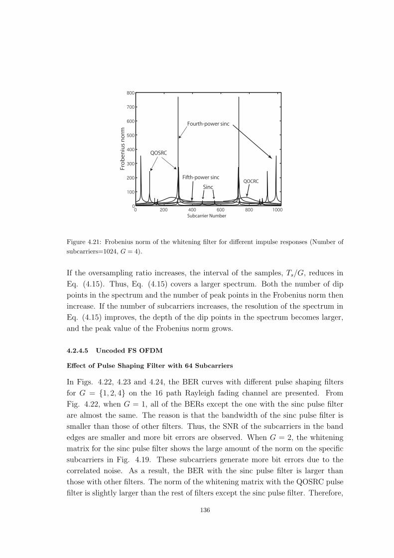
Figure 4.21: Frobenius norm of the whitening filter for different impulse responses (Number ofsubcarriers=1024, G = 4).
If the oversampling ratio increases, the interval of the samples, Ts/G, reduces in
Eq. (4.15). Thus, Eq. (4.15) covers a larger spectrum. Both the number of dip
points in the spectrum and the number of peak points in the Frobenius norm then
increase. If the number of subcarriers increases, the resolution of the spectrum in
Eq. (4.15) improves, the depth of the dip points in the spectrum becomes larger,
and the peak value of the Frobenius norm grows.
4.2.4.5 Uncoded FS OFDM
Effect of Pulse Shaping Filter with 64 Subcarriers
In Figs. 4.22, 4.23 and 4.24, the BER curves with different pulse shaping filters
for G = {1, 2, 4} on the 16 path Rayleigh fading channel are presented. From
Fig. 4.22, when G = 1, all of the BERs except the one with the sinc pulse filter
are almost the same. The reason is that the bandwidth of the sinc pulse filter is
smaller than those of other filters. Thus, the SNR of the subcarriers in the band
edges are smaller and more bit errors are observed. When G = 2, the whitening
matrix for the sinc pulse filter shows the large amount of the norm on the specific
subcarriers in Fig. 4.19. These subcarriers generate more bit errors due to the
correlated noise. As a result, the BER with the sinc pulse filter is larger than
those with other filters. The norm of the whitening matrix with the QOSRC pulse
filter is slightly larger than the rest of filters except the sinc pulse filter. Therefore,
136

Figure 4.22: BER performance vs. Eb/N0 on the 16 path Rayleigh fading channel with theuniform delay profile (QPSK, Number of subcarriers=64, G = 1).
Figure 4.23: BER performance vs. Eb/N0 on the 16 path Rayleigh fading channel with theuniform delay profile (QPSK, Number of subcarriers=64, G = 2).
the BER performance is also slightly worse.
When G = 4, BER performances of QOSRC pulse filter and the fourth-power
sinc pulse filter are deteriorated. From Fig. 4.20, the norm with the QOSRC pulse
137

Figure 4.24: BER performance vs. Eb/N0 on the 16 path Rayleigh fading channel with theuniform delay profile (QPSK, Number of subcarriers=64, G = 4).
Figure 4.25: BER performance vs. Eb/N0 on the 16 path Rayleigh fading channel with theuniform delay profile (16QAM, Number of subcarriers=64, G = 4).
filter shows the largest and the fourth-power sinc pulse filter shows the second
largest on the specific subcarriers. On those subcarriers more bit errors are pro-
138

Figure 4.26: BER performance vs. Eb/N0 on the 16 path Rayleigh fading channel with theuniform delay profile (64QAM, Number of subcarriers=64, G = 4).
duced. Even though Eb/N0 increases, the BER does not reduce as those with the
QOCRC pulse filter or the fifth-power sinc pulse filter. Therefore, the BER curves
for those pulse filters in Fig. 4.24 are worse than those with the other filters except
the sinc pulse filter. For the case of the sinc pulse filter, the bandwidth of the filter
is smaller than the others as shown in Fig. 4.19. It is suggested in [4.6] that the
excess bandwidth of the filter allows diversity gain in FS. The BER with the sinc
pulse filter is then larger than those with the QOCRC pulse filter or fifth-power
sinc pulse filter that has larger bandwidth.
Through Figs. 4.22-4.24, no diversity gain can be obtained with the root cosine
roll-off filter. It has been suggested in [4.6] that the excessive bandwidth of the
filter gives diversity gain with FS. Thus, the sharp frequency response of the root
cosine filter limits diversity gain.
Figures 4.25 and 4.26 show the BER curves with different pulse shaping filters
for G = 4 when 16QAM or 64QAM modulation is employed. In those figures, the
same tendency on the BER performance can be observed as the case with QPSK
modulation for G = 4. As far as we have investigated, when G = {1, 2}, the BER
performance with 16QAM or 64QAM also shows the same tendency as the case
with QPSK.
139

Figure 4.27: BER performance vs. Eb/N0 on the 16 path Rayleigh fading channel with theuniform delay profile (QPSK, Number of subcarriers=1024, G = 4).
Figure 4.28: BER performance vs. Eb/N0 on the 16 path Rayleigh fading channel with theuniform delay profile (16QAM, Number of subcarriers=1024, G = 4).
Effect of Pulse Shaping Filter with 1024 Subcarriers
The effect of the pulse shaping filters with larger numbers of subcarriers are also
investigated. In Fig. 4.27, the BER curves with different pulse shaping filters for140

Figure 4.29: BER performance vs. Eb/N0 on the 16 path Rayleigh fading channel with theuniform delay profile (64QAM, Number of subcarriers=1024, G = 4).
Figure 4.30: BER performance vs. Eb/N0 on the 24 path Rayleigh fading channel with theexponential delay profile (QPSK, Number of subcarriers=1024, G = 4).
G = 4 are presented. The channel model we assume here is 16 path Rayleigh
fading with a uniform delay profile. When G = 4, the curves of the Frobenius
141

Figure 4.31: BER performance vs. Eb/N0 on the GSM Typical Urban model (QPSK, Numberof subcarriers=1024,G = 4).
norm of the whitening filters shown in Fig. 4.21 are different as compared to those
in Fig. 4.20. In this case, the norm with the fourth-power sinc pulse filter shows
the largest and the one with QOSRC pulse filter shows the second largest on the
specific subcarriers. On those subcarriers more bit errors are produced. However,
the BERs do not increase significantly in Fig. 4.27 as compared to those in Fig.
4.24. For the cases of the fourth-power sinc pulse filter and the QOSRC pulse filter,
though the bit error rates on some particular subcarriers are larger, it is averaged
over the BERs of the large number of subcarriers. On the other hand, the BER
with the sinc filter is larger than those with other filters because of the smaller
bandwidth and limited diversity gain. When G = {1, 2}, the same tendency on
the BER performance can be observed as the cases with 64 subcarriers.
Figures 4.28 and 4.29 show the BER curves with different pulse shaping filters
on the 16 path Rayleigh fading channel model when 16QAM or 64QAM modulation
is applied. In those figures, the same tendency on the BER performance can be
observed as the case with QPSK modulation for G = 4.
Figures 4.30 and 4.31 show the BER performance for QPSK modulation with
different pulse shaping filters on the 24 path Rayleigh fading channel model and
the GSM Typical Urban model. In those figures, the same as the case with the
16 path Rayleigh fading channel model, the BER degradation due to the different
pulse shaping filters is smaller than that of the OFDM system with 64 subcarriers.
142

Since the number of multipath is smaller for the GSM model than the Rayleigh
fading channel model, diversity gain through FS is smaller in Fig. 4.31. Thus, the
BER curves for all the impulse responses of the filter are a little worse than those
in Fig. 4.30.
4.2.4.6 Coded FS OFDM
Figure 4.32 shows the BER curves of the coded FS OFDM with different impulse
responses of the pulse shaping filter. The number of subcarriers is 64 and the
oversampling ratio is set to G = 4, here. A rate 1/2 convolutional code with its
generating matrix G = [1338, 1718] and interleaving specified in the IEEE 802.11a
standard are employed [4.15]. Soft decision Viterbi decoding is performed in the
receiver. As compared to Fig. 4.24, the improvement of the BER curves for the
QOSRC and fourth-power sinc pulse filters are limited. This is because the effect
of the large Frobenius norm is spread over the subcarriers due to the channel
coding and the interleaving. To reduce the effect of the large Frobenius norm,
the metric in the Viterbi decoder is adjusted according to the Frobenius norm on
each subcarrier. Figure 4.33 shows the BER curves of the coded FS OFDM with
the adjusted metric. In this figure, the BER curves with the QOSRC and fourth-
power sinc pulse filters are improved as compared to those in Fig. 4.32. The metric
adjustment can mitigates the effect of the large Frobenius norm.
Figure 4.34 shows the BER curves of the coded FS OFDM with different impulse
responses of the pulse shaping filter when the number of subcarriers is 1024. Figure
4.35 shows the BER curves of the coded FS OFDM with the adjusted metric
according to the Frobenius norm. A rate 1/2 convolutional code with its generating
matrix G = [1338, 1718] and interleaving specified in the IEEE 802.16 standard
are employed [4.16]. In those figures, the same as the coded system, the BER is
averaged over the large number of subcarriers and the difference due to the pulse
shaping filters is smaller than that of the system with 64 subcarriers.
143

Figure 4.32: BER performance vs. Eb/N0 of coded OFDM (QPSK, Number of subcarriers=64,G = 4).
Figure 4.33: BER performance vs. Eb/N0 of coded OFDM with Adjusted Metric (QPSK, Numberof subcarriers=64, G = 4).
144

Figure 4.34: BER performance vs. Eb/N0 of coded OFDM (QPSK, Number of subcarriers=1024,G = 4).
Figure 4.35: BER performance vs. Eb/N0 of coded OFDM with Adjusted Metric (QPSK, Numberof subcarriers=1024, G = 4).
145

4.2.5 Conclusions
In this section, the effect of the pulse shaping filters on the FS OFDM system with
subcarrier-based MRC has been investigated. The Frobenius norm of the whiten-
ing filter closely corresponds to the frequency spectrum of the pulse shaping filter.
It has been shown that the Frobenius norm of the whitening matrix has significant
effect on the BER performance irrespective of modulation schemes and channel
models. If the Frobenius norm is large, the power of the correlated noise compo-
nents increases and the BER on the corresponding subcarrier is deteriorated. If
the number of subcarriers is 64, the average BER also increases. When the number
of subcarriers is 1024, the large amount of the Frobenius norm is concentrated on
the specific subcarriers. Although the higher number of bit errors can be observed
on those subcarriers, it is less significant to the average BER if the number of
subcarriers is large.
When the channel coding is employed, the large Frobenius norm deteriorates the
total BER performance of the system with 64 subcarriers. It has also been shown
that the Viterbi decoder with the adjusted metric according to the Frobenius norm
improves the BER performance.
As a conclusion, it is required to design the pulse shaping filters in order to
reduce the amount of the correlated noise caused by the Frobenius norm and
to obtain diversity gain. The Frobenius norm can be calculated at the stage of
designing the pulse shaping filters. Moreover, when the number of subcarrier is
small and the pulse shaping filter introduces the large amount of the Frobeinus
norm on the specific subcarriers, the adjusted metric based on the Frobenius norm
can mitigate the effect of the correlated noise components in the coded FS OFDM
system.
4.3 Conclusions of Chapter 4
In Chapter 4, the correlated noise cancellation schemes in the FS OFDM system
have been investigated. Despreading with the ASC cancels most of the correlated
noise components in the FS OFCDM system. The performance of FS OFDM
receiver can be improved by designing the parameters such as the bandwidth, the
Frobenius norm of the whitening matrix corresponding to the impulse response
of the pulse shaping filter, and the number of subcarriers. Moreover, the Viterbi
decoder with the adjusted metric according to the Frobenius norm improves the
BER performance of the coded FS OFDM system. It has been also shown that
the effect of correlated noise can be reduced both in FS OFCDM and FS OFDM
146

systems.
4.4 References
[4.1] H. Atarashi and M. Sawahashi, “Investigation of Inter-Carrier Interference
due to Doppler Spread in OFCDM Broadband Packet Wireless Access”,
IEICE Trans. on Commun., vol.E85-B, no.12, pp.2684-2693, Dec. 2002.
[4.2] H. Atarashi, S. Abeta, and M. Sawahashi, “Variable Spreading Factor-
Othogonal Frequency and Code division Multiplexing (VSF-OFCDM) for
Broadband Packet Wireless Access”, IEICE Trans. on Commun., vol.E86-
B, no.1, pp.291-299, Dec. 2003.
[4.3] Y. Kishiyama, N. Maeda, K. Higuchi, H. Atarashi, and M. Sawahashi, “Field
Experiments on Throughput Performance above 100 Mbps in Forward Link
for VSF-OFCDM Broadband Wireless Access”, IEICE Trans. on Commun.,
vol.E88-B, no.2, pp.604-614, Feb. 2005.
[4.4] N. Maeda, H. Atarashi, S. Abeta, and M. Sawahashi, “Antenna Diversity
Reception Appropriate for MMSE Combining in Frequency Domain for For-
ward Link OFCDM Packet Wireless Access”, IEICE Trans. on Commun.,
vol.E85-B, no.10, pp.1966-1977, Oct. 2002.
[4.5] N. Miki, H. Atarashi, and M. Sawahashi, “Effect of Time Diversity in Hy-
brid ARQ Considering Space and Path Diversity for VSF-OFCDM Down-
link Broadband Wireless Access”, Proc. of the 15th IEEE Symposium on
Personal Indoor and Mobile Radio Communications 2004, pp.604-608 vol.1,
Sep. 2004.
[4.6] C. Tepedelenlioglu and R. Challagulla, “Low-Complexity Multipath Diver-
sity Through Fractional Sampling in OFDM,” IEEE Trans., on Signal Pro-
cessing, vol.52, no.11, pp.3104- 3116, Nov. 2004.
[4.7] Y. Kato, M. Inamori, and Y. Sanada, “Multipath Diversity through Frac-
tional Sampling in MB-OFDM,” Proc. of the 5th IEEE VTS Asia Pacific
Wireless Communications Symposium, Aug. 2008.
[4.8] K. Suto and T. Otsuki, “Space-Time-Frequency Block Codes over Frequency
Selective Fading Channels,” IEICE Trans. on Commun., vol.E86-B, no.7,
pp.1939-1945, July 2004.
147

[4.9] M. Inamori, H. Nishimura, Y. Sanada, and M. Ghavami, “Fractional Sam-
pling OFCDM with Alternative Spreading Code,” Proc. of the 11th IEEE
International Conference on Communications Systems, pp.1394-1398, Nov.
2008.
[4.10] G. Golub and C. V. Loan, “Matrix Computations,” 3rd Edition, Johns
Hopkins University Press, 1996.
[4.11] S. L. Loyka, “Channel Capacity of MIMO Architecture using the Exponen-
tial Correlation Matrix,” IEEE Communications Letters, vol.5, no.9, pp.369-
371, Sept. 2001.
[4.12] M. Chiani, M. Z. Win, and A. Zanella, “On the Capacity of Spatially Corre-
lated MIMO Rayleigh-fading Channels,” IEEE Trans. on Information The-
ory, vol.49, no.10, pp.2363-2371, Oct. 2003.
[4.13] K. Zhang, Y. L. Guan, and B. C. Ng, “Full-Rate Orthogonal Space Time
Block Code With Pulse-Shaped Offset QAM for Four Transmit Antennas,”
IEEE Trans. on Wireless Communications, vol.6, no.4, pp.1551-1559, April
2007.
[4.14] I. Sasase, R. Nagayama, and S. Mori, “Bandwidth Efficient Quadrature
Overlapped Squared Raised-Cosine Modulation,” IEEE Trans. on Wireless
Communications, vol.33, pp.101-103, Jan. 1985.
[4.15] Part 11: Wireless LAN Medium Access Control (MAC) and Physical Layer
(PHY) Specifications; Highspeed Physical Layer in the 5GHz Band, 1999,
IEEE.802.11a.
[4.16] Part 16: Air Interface for Fixed Broadband Wireless Access Systems, 2004,
IEEE Std. 802.16.
148
Chapter 5
Overall Conclusions
OFDM system has been employed in many wireless standards to achieve high data
rate transmission. In OFDM receivers, the received signal suffers from distortions
due to RF components, timing jitter, or baseband filters. To implement a low cost
and low power consumption receiver, the compensation of the signal distortion in a
digital domain is necessary. In this dissertation, the digital compensation schemes
for the signal distortion in OFDM receivers were investigated.
5.1 Signal Compensation Schemes in OFDM Direct Con-
version Receivers
Digital compensation schemes for the signal distortion due to RF components in
direct conversion receiver are presented in Chapter 2. The OFDM direct con-
version receivers suffer from the frequency and DC offsets. In Section 2.1, the
frequency offset estimation in the presence of time-varying DC offset for OFDM
direct conversion receivers has been presented. The frequency offset is estimated
based on the preamble symbols in the IEEE 802.11a burst structure. In the pro-
posed scheme, the differential filter is employed to remove the dynamic DC offset.
It has been shown that the residual DC offset is eliminated with the differential
filter by setting the optimum threshold level. The frequency offset can be then esti-
mated accurately with simple calculation. The proposed compensation scheme has
offered the superior frequency offset estimation as compared with the conventional
scheme with high pass filter.
The OFDM direct conversion receiver also suffers from the IQ imbalance as well.
The IQ imbalance deteriorates the performance of the frequency offset estimation
scheme with the differential filter. In Section 2.2, the frequency offset estimation
149

with the differential filter in the presence of IQ imbalance has been analyzed.
The numerical results obtained through computer simulation have shown that the
derived analysis provides close approximation to the performance of the frequency
offset estimation scheme. It has also clarified the dependency of the MSE on the
waveform of the preamble symbols, which is caused by the IQ imbalance.
In Section 2.3, the IQ imbalance estimation in the presence of the frequency
and DC offsets for the OFDM direct conversion receiver has been discussed. The
same differential filter has been employed to remove the time-varying DC offset
as in Section 2.1 and Section 2.2. The IQ imbalance is estimated using a simple
equation without the impulse response of the channel. The numerical results ob-
tained through computer simulations has shown that the BER performance using
the proposed IQ imbalance estimation scheme is satisfactory when Eb/N0 is higher
than 20[dB], in which 64QAM is used for the 1st modulation. However, the ac-
curacy of the IQ imbalance estimation with the proposed scheme is deteriorated
when the frequency offset is small. To overcome this problem, the new IQ imbal-
ance estimation scheme in frequency domain is proposed in Section 2.4. The IQ
imbalance is estimated with pilot subcarriers in data period. Numerical results
obtained through computer simulation show that the estimation accuracy and the
BER performance can be improved even if the frequency offset is small. Thus, the
combination of two low-complexity IQ imbalance estimation schemes is suitable
for low-cost and low-power-comsumption direct conversion receivers.
In Chapter 2, it is shown that the frequency offset and IQ imbalance are es-
timated well by the simple calculation with the differential filter. These signal
compensation schemes enable the low-cost and low-power-comsumption direct con-
version receivers.
5.2 Signal Compensation Schemes in RF-sampling Receivers
In contrast to the front end of the direct conversion receiver, the RF-sampling re-
ceiver is greatly simplified with digital RF processing. However, the RF-sampling
receiver suffers from the timing jitter generated from the phase noise in PLL. In
Chapter 3, the effect of timing jitter on quadrature charge sampling has been dis-
cussed. The distributions of timing jitter based on the structure of two major noise
sources, which are VCO and TCXO in the PLL. The SINR of the downconverted
signal has been evaluated with different data rates and modulation schemes. It
has been shown that timing jitter deteriorates the SINR of the demodulated signal
due to the crosstalk between the I-phase and Q-phase components of the received
150

signal. The BER performances with both single carrier QAM and OFDM modu-
lation schemes has shown the error floor with higher data rates. Therefore, in the
wideband system, the timing jitter in quadrature charge sampling may limit the
performance of the receiver.
5.3 Signal Compensation Schemes in FS OFDM Receivers
One of the important factors of the receiver architecture is the better BER per-
formance. The OFDM receiver can improve the performance with diversity. The
antenna diversity has been receiving large attention, which is standardized in the
physical layer of IEEE 802.11n. However, it is hard to implement multiple anten-
nas in small devices. As the diversity scheme with a single antenna, FS OFDM
system has been investigated. However, as the number of subcarriers and the over-
sampling ratio increase, the correlation among the noise components over different
subcarriers deteriorates the BER performance. Chapter 4 discusses the correlated
noise cancelation schemes in FS OFDM receivers. In Section 4.1, the correlated
noise cancellation scheme in FS OFCDM system has been discussed. To reduce the
correlated noise, ASC, which has positive and negative components alternatively,
is used in the FS OFCDM system. Despreading with the ASC cancels most of
the correlated noise components. Numerical results obtained through computer
simulation show that the proposed scheme can improve the performance of the
receiver with the large oversampling ratio and the number of subcarriers.
In Section 4.2, the effect of the correlation among the noise components in
the FS OFDM system has been investigated. The impulse response of the filter
determines the correlation among the noise components because the noise passes
through the pulse shaping filter in the receiver. To evaluate the effect of corre-
lation among the noise components, five pulse shaping filters are applied to both
the FS OFDM and coded FS OFDM systems. Numerical results obtained through
computer simulations has shown that the Frobenius norm of a whitening matrix
corresponding to the pulse shaping filter has significant effect on the BER per-
formance especially with a small numbers of subcarriers. It has also been shown
that the Viterbi decoder with the adjusted metric according to the Frobenius norm
improves the BER performance of the coded FS OFDM system. The BER per-
formance depends on two facts, which are diversity gain and the Frobenius norm.
The Frobenius norm can be calculated at the stage of designing the pulse shaping
filters. The high-performance FS OFDM receiver can be realized by designing the
parameters such as the bandwidth, the Frobenius norm of the whitening matrix
151

corresponding to the impulse response of the pulse shaping filter, and the number
of subcarriers.
152

Acknowledgements
This dissertation has been a long journey. I have endured and completed this
journey with the help and support from numerous people around me.
This dissertation would not have been possible if not for the stimulating sugges-
tions and encouragement given to me by my supervisor Prof. Yukitoshi Sanada.
I am indebted to his diligence and patience in constantly guiding me towards the
completion of this dissertation and beyond. If not for his careful supervision, this
dissertation could not boast the number of contributions it has achieved.
Furthermore, I would also like to express my gratitude for the referees who
examined this dissertation, Prof. Sasase, Prof. Nakagawa, Prof. Ishikuro and
Prof. Ghavami. Their critical review and constructive suggestions added an extra
layer of polish to this dissertation.
I would like to thank my co-researchers Mr. M. Abe, Mr. K. Saijo, Mr. H.
Yokoshima and Mr. Y. Kondo from Sony Corporation for their suggestions and
discussions. Our joint research started when I was just a bachelor course student
and it has been a great experience to have worked with them for so many years.
As a member of Sanada Laboratory, I would also like to take advantage of this
opportunity to express my thanks towards my other colleagues for their support
and encouragement. Particularly, I would like to thank my doctoral colleague,
Caglar, for his encouragements in overcoming the challenges associated with the
degree. I was able to enjoy my doctorate studies because of the warmth and family-
like atmosphere in the lab. I would also like to express my appreciation my fellow
Research Assistants (RAs) in the GCOE program, Mr. K. Adachi, Maduranga,
Mr. S. Iwamura, Mr. K. Kyochi, Alex, Parn and Safda, for the stimulating research
discussions that helped give my research some perspective.
However, life is not all work and no play. There are other external elements
that have supported me as well throughout this journey. I would like to thank Ken
for taking time out to proofread certain parts of this dissertation. I would also like
to thank my good friend Mari for her support.
Last but not least, I wish to express my heartfelt thanks to my family who have
153

always been a great source of support and and encouragement for me.
154

List of Achievements
Journal Publications
1. M. Inamori, A. M. Bostamam, and Y. Sanada, “Influence of Timing Jitter on
Quadorature Charge Sampling,” IET Communications, Vol.1, No.4, pp.705-
710, Aug. 2007.
2. M. Inamori, A. M. Bostamam, Y. Sanada, and H. Minami, “Frequency Offset
Estimation Scheme in the Presence of Time-varying DC Offset for OFDM
Direct Conversion Receivers,” IEICE Trans. on Communications, Vol.E90-B,
No.10, pp.2884-2890, Oct. 2007.
3. M. Inamori, T. Kawai, T. Kobayashi, H. Nishimura, and Y. Sanada, “Ef-
fect of Pulse Shaping Filters on a Fractional Sampling OFDM System with
Subcarrier-Based Maximal Ratio Combining,” IEICE Trans. on Communica-
tion, vol.E92-B, no.5, pp.1484-1494, May 2009.
4. M. Inamori, A. M. Bostamam, Y. Sanada, and H. Minami, “IQ Imbalance
Compensation Scheme in the Presence of Frequency Offset and Dynamic DC
Offset for a Direct Conversion Receiver,” IEEE Trans. on Wireless Commu-
nications, Vol.8, no.5, pp.2214-2220, May 2009.
5. M. Inamori, S. Takayama, and Y. Sanada, “IQ Imbalance Estimation Scheme
in the Presence of DC Offset and Frequency Offset in the Frequency Domain,”
accepted to IEICE Trans. on Fundamentals.
Other Journal Publications
1. Y. Suzuki, A. M. Bostamam, M. Inamori, and Y. Sanada, “Direct-Sequence
/ Spread-Spectrum Communication System with Sampling Rate Selection
Diversity,” IEICE Trans. on Communications, Vol.E91-B, No.1, pp.267-273,
Jan. 2008.
155

2. H. Nishimura, M. Inamori, and Y. Sanada, “Sampling Rate Selection for Frac-
tional Sampling in OFDM,” IEICE Trans. on Communications, Vol.E91-B,
No.9, pp.2876-2882, Sept. 2008.
Conference Publications
1. M. Inamori, A. M. Bostamam, and Y. Sanada, “Influence of Sampling Jitter
on Discrete Time Receiver,” in Proc. the 16th Annual International Sym-
posium on Personal Indoor and Mobile Radio Communications, Berlin, Ger-
many, Sept. 2005.
2. M. Inamori, A. M. Bostamam, Y. Sanada, and H. Minami, “Frequency Off-
set Compensation Scheme under DC Offset for OFDM Direct Conversion
Receivers,” in Proc. the 9th International Symposium on Wireless Personal
Multimedia Communications, pp.378-382, San Diego, USA, Sept. 2006.
3. M. Inamori, A. M. Bostamam, Y. Sanada, and H. Minami,”Frequency Offset
Estimation Scheme in the Presence of Time-varying DC Offset and IQ Im-
balances for OFDM Direct Direct Conversion Receivers,” in Proc. the 18th
Annual International Symposium on Personal Indoor and Mobile Radio Com-
munications, Athens, Greece, Sept. 2007.
4. M. Inamori, H. Nishimura, Y. Sanada, and M. Ghavami, “Fractional Sam-
pling OFCDM with Alternative Spreading Code,” in Proc. the 11th IEEE
International Conference on Communications Systems, Guangzhou, China,
Nov. 2008.
5. M. Inamori, T. Kawai, T. Kobayashi, H. Nishimura, and Y. Sanada, “Effect
of Frobenius Norm of Whitening Matrix on Fractional Sampling OFDM with
Subcarrier-Based Maximal Ratio Combining,” in Proc. the 2009 RISP In-
ternational Workshop on Nonlinear Circuits and Signal Processing, Hawaii,
U.S.A., March 2009.
6. M. Inamori, A. M. Bostamam, Y. Sanada, and H. Minami, “IQ Imbalance
Compensation Scheme in the Presence of Frequency Offset and Dynamic DC
Offset for a Direct Conversion Receiver,” in Proc. the 69th IEEE Vehicular
Technology Conference, Barcelona, Spain, April 2009.
7. M. Inamori, T. Kawai, T. Kobayashi, H. Nishimura, and Y. Sanada, “Metric
Weighting Scheme on a Coded Fractional Sampling OFDM System,” in Proc.
156

the the 70th IEEE Vehicular Technology Conference, Anchorage, U.S.A.,
Sept. 2009. [accepted]
8. M. Inamori, A. M. Bostamam, and Y. Sanada, “Performance of Frequency
Offset Estimation in the Presence of IQ Imbalance for OFDM Direct Con-
version Receivers,” in Proc. 2009 IEEE Pacific Rim Conference on Commu-
nications, Computers and Signal Processing, Victoria, Canada, Aug. 2009.
[accepted]
9. M. Inamori and Y. Sanada, “Effect of Pulse Shaping Filter on MB-OFDM
with Fractional Sampling,” in Proc. the 12th International Symposium on
Wireless Personal Multimedia Communications, Sendai, Sept. 2009. [ac-
cepted]
10. M. Inamori, S. Takayama, and Y. Sanada, “Frequency Domain IQ Imbalance
Estimation in the Presence of DC Offset and Frequency Offset,” in Proc. the
20th IEEE International Symposium On Personal, Indoor and Mobile Radio
Communications, Tokyo, Sept. 2009. [accepted]
Other Conference Publications
1. Y. Suzuki, A. M. Bostamam, M. Inamori, and Y. Sanada, “Sampling Rate
Selection Diversity for Direct-Sequence Spread Spectrum,” in Proc. SDR
Technical Conference 2006, Orlando, USA, Nov. 2006.
2. H. Nishimura, M. Inamori, and Y. Sanada, “Sampling Rate Selection for Frac-
tional Sampling in OFDM,” in Proc. the 18th Annual International Sympo-
sium on Personal Indoor and Mobile Radio Communications, Athens, Sept.
2007.
3. Y. Kato, M. Inamori, and Y. Sanada, “Multipath Diversity Through Frac-
tional Sampling in MB-OFDM,” in Proc. the 5th IEEE VTS Asia Pacific
Wireless Communications Symposium, Sendai, Japan, Aug. 2008.
4. Y. Suzuki, A. M. Bostamam, M. Inamori, and Y. Sanada, “Sampling Rate
Selection Path Diversity for a RAKE Receiver in DS/SS,” in Proc. the 68th
IEEE Vehicular Technology Conference, Calgary, Canada, Sept. 2008.
5. H. Nishimura, M. Inamori, and Y. Sanada, “Initial Sampling Point Selection
in OFDM Receiver with Fractional Sampling,” in Proc. International Work-
shop on Vision, Communications and Circuits, Xi’an, China, Nov. 2008.
157

6. T. Shinkai, H. Nishimura, M. Inamori, and Y. Sanada, “Experimental Inves-
tigation of Fractional Sampling in IEEE802.11a WLAN System,” in Proc. the
11th IEEE International Conference on Communications Systems, Guangzhou,
China, Nov. 2008.
7. H. Nishimura, M. Inamori, Y. Sanada, and M. Ghavami, “Non-uniform Sam-
pling Point Selection in OFDM Receiver with Fractional Sampling,” in Proc.
2009 IEEE Pacific Rim Conference on Communications, Computers and Sig-
nal Processing, Victroia, Aug. 2009. [accepted]
8. A. Suzuki, M. Inamori, and Y. Sanada, “Symbol Weighting Scheme in OFDM
Receiver with Sigma-Delta A/D Converter,” in Proc. the 12th International
Symposium on Wireless Personal Multimedia Communications, Sendai, Sept.
2009. [accepted]
Technical Reports
1. M. Inamori, A. M. Bostamam, Y. Sanada, “Influence of Sampling Jitter on
the Discrete Time Receiver, “ Technical Reports of IEICE, SR2004-21, March
2005.
2. M. Inamori. M. Bostamam, Y. Sanada, “Influence of Sampling Jitter on the
Discrete Time Receiver, “ IEICE General Conference, B-17-2, March 2005.
3. M. Inamori, A. M. Bostamam, Y. Sanada, H. Minami, “Frequency Offset
Estimation Scheme in the presence of Time-varying DC offset for OFDM
Direct Conversion Receivers , “ Technical Reports of IEICE, SR2006-50, Nov.
2006.
4. M. Inamori, A. M. Bostamam, Y. Sanada, H. Minami, “Frequency Offset Es-
timation Scheme in the Presence of Time-varying DC Offset and IQ Imbalance
for OFDM Direct Conversion Receivers, “ Technical Reports of IEICE,SR2007-
15, May 2007.
5. M. Inamori, Y. Sanada, “Study of Pulse Shaping Filter on MB-OFDM with
Fractional Sampling,” Technical Reports of IEICE,WBS2007-42, Oct. 2007.
6. M. Inamori, A. M. Bostamam, Y. Sanada, H. Minami, “IQ Imbalance Esti-
mation Scheme in the Presence of DC Offset and Frequency Offset for OFDM
Direct Conversion Receivers,” Technical Reports of IEICE, SR2007-54, Nov.
2007.
158

7. M. Inamori, A. M. Bostamam, Y. Sanada, H. Minami, “IQ Imbalance Es-
timation Scheme in the Presence of Time-varying DC offset and Frequency
Offset for OFDM Direct Conversion Receivers,” Technical Reports of IEICE,
SR2007-78, Jan. 2008.
8. M. Inamori, H. Nishimura, Y. Sanada, “Alternative Spreading Code for Frac-
tional Sampling OFCDM, “ Technical Reports of IEICE, SR2008-12, May
2008.
9. M. Inamori, T. Kawai, T. Kobayashi, H. Nishimura, Y. Sanada, “Effect of
pulse shaping filters on fractional sampling OFDM systems with subcarrier-
based maximal ratio combining,” Technical Reports of IEICE, SR2008-42,
Oct. 2008.
10. M. Inamori, Y. Sanada, “Performance Analysis of Frequency Offset Estima-
tion in the Presence of DC Offset and IQ Imbalance for OFDM Direct Con-
version Receivers,” Technical Reports of IEICE, SR2008-90, March 2009.
11. M. Inamori, K. Takashi, T. Kobayashi, H. Nishimura, Y. Sanada, “Met-
ric Weighting Scheme on a Fractional Sampling Coded OFDM System with
Subcarrier-Based Maximal Ratio Combining,” IEICE General Conference, B-
17-22, March 2009.
12. M. Inamori, S. Takayama, Y. Sanada, “Frequency Domain IQ Imbalance Esti-
mation Scheme in the Presence of DC Offset and Frequency Offset,” Technical
Reports of IEICE, SR2009-05, May 2009.
13. M. Inamori, S. Takayama, Y. Sanada, “Frequency Domain IQ Imbalance Es-
timation Scheme in the Presence of DC Offset and Frequency Offset,” IEICE
Society Conference, ABS-1-8, Sept. 2009.
Other Technical Reports
1. Y. Suzuki, A. M. Bostamam, M. Inamori, Y. Sanada, “DS/SS Communication
System with Sampling Rate Selection Diversity,” Technical Reports of IEICE,
SR2006-51, Nov. 2006.
2. H. Nishimura, M. Inamori, Y. Sanada, “Sampling Rate Selection for Frac-
tional Sampling in OFDM,” Technical Reports of IEICE, SR2007-1, May
2007.
159
3. H. Nishimura, M. Inamori, Y. Sanada, “Sampling Rate Selection for Frac-
tional Sampling in OFDM,” Japan Society for Simulation Technology Con-
ference, 11-1, June 2007.
4. H. Nishimura, M. Inamori, Y. Sanada, “Sampling Point Selection in OFDM
Receiver with Fractional Sampling,” Technical Reports of IEICE, SR2007-87,
March 2008.
5. Y. Suzuki, A. M. Bostamam, M. Inamori, Y. Sanada, “Sampling Rate Selec-
tion for a RAKE Receiver in DS/SS,” Technical Reports of IEICE, SR2007-88,
March 2008.
6. Y. Suzuki, A. M. Bostamam, M. Inamori, Y. Sanada, “Sampling Rate Se-
lection for a RAKE Receiver in DS/SS,” IEICE General Conference, BS-1-9,
March 2008.
7. H. Nishimura, M. Inamori, Y. Sanada, “Sampling Point Selection in OFDM
Receiver with Fractional Sampling,” IEICE General Conference, BS-1-10,
March 2008.
8. T. Shinkai, H. Nishimura, M. Inamori, Y. Sanada, “Experimental Investi-
gation of Fractional Sampling in IEEE802.11a WLAN System, “ Technical
Reports of IEICE, SR2008-28, July 2008.
9. H. Nishimura, M. Inamori, Y. Sanada, M.Ghavami, “Non-uniform Sampling
Point Selection in OFDM Receiver with Fractional Sampling,” Technical Re-
ports of IEICE, SR2008-41, Oct. 2008.
10. H. Nishimura, M. Inamori, Y. Sanada, “Complexity Reduction Scheme for
Sampling Point Selection in Fractional Sampling OFDM Receiver,” IEICE
General Conference, B-17-23, March 2009.
11. A. Suzuki, M. Inamori, Y. Sanada, “Symbol Weighting Scheme in OFDM
Receiver with Sigma-Delta A/D Converter,” Technical Reports of IEICE,
WBS2009-2, June 2009.
12. R. C. Kizilirmak, M. Inamori, and Y. Sanada, “Spatial Fading Correlation
for OFDM Antenna Arrays on a per Subcarrier Basis,” IEICE Society Con-
ference, ABS-1-8, Sept. 2009.
Awards
1. NCSP 2009 Student Paper Award, March 2009.
160

2. IEEE VTS Japan 2009 Student Paper Award, April 2009.
161


