29
D IGITAL D ELAY - L OCKED L OOP D ESIGN for SDRAM YUN LAN ECG 721 11/18/2015 1
DIGITAL DELAY-LOCKED LOOP DESIGN for SDRAM
YUN LAN
ECG 721
11/18/2015 1

Outline DLL Introduction
DRAM and SDRAM
Design of All Digital DLL Operation
Design of the components
Simulations
Design Considerations
2
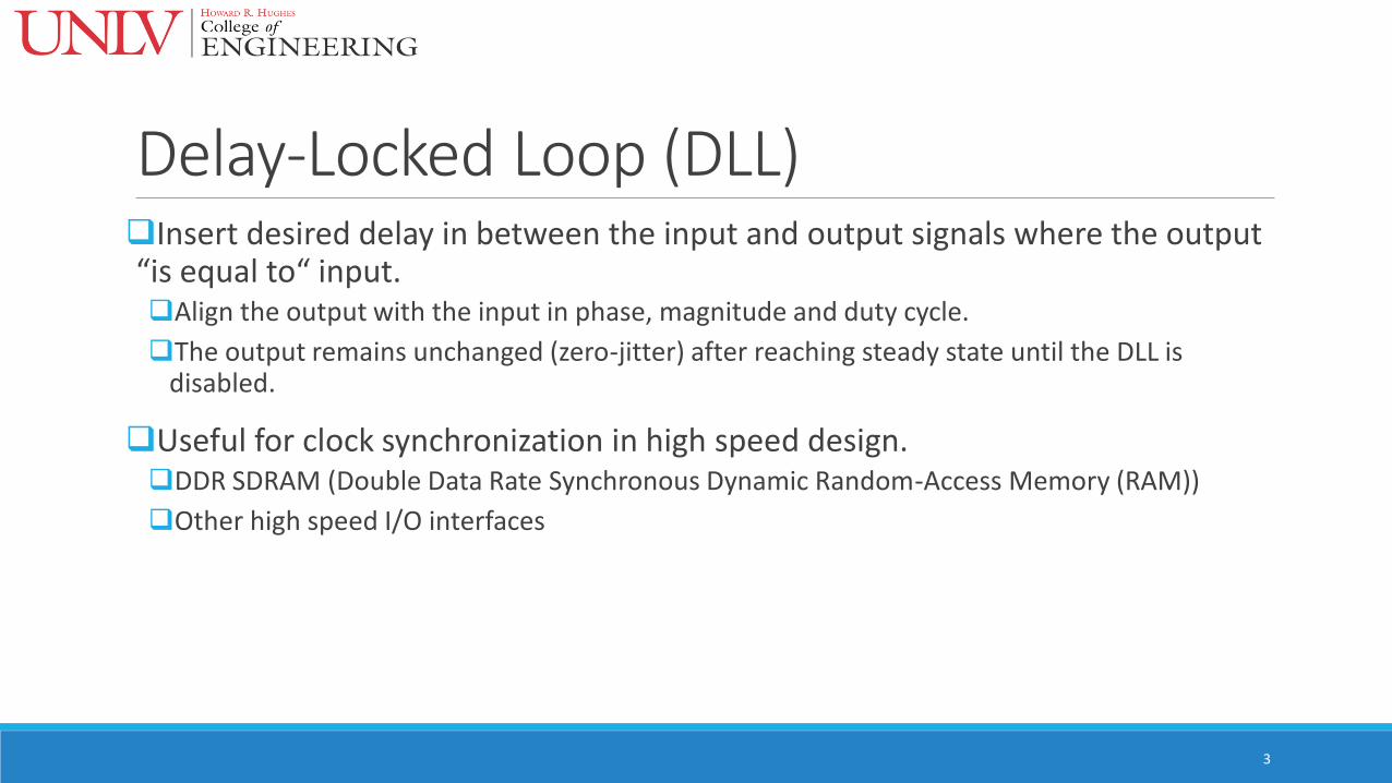
Delay-Locked Loop (DLL) Insert desired delay in between the input and output signals where the output “is equal to“ input. Align the output with the input in phase, magnitude and duty cycle.
The output remains unchanged (zero-jitter) after reaching steady state until the DLL is disabled.
Useful for clock synchronization in high speed design. DDR SDRAM (Double Data Rate Synchronous Dynamic Random-Access Memory (RAM))
Other high speed I/O interfaces
3
DLL for SDRAM What is SDRAM and its operations?
Why is the DLL needed for SDRAM?
4

DRAM to SDRAM Refer DRAM basics in textbook.
DRAM operations Commands: Read, Write and Refresh.
Refresh/Self Refresh: charge/discharge all the capacitive cells every once in a while to keep the contents staying at full logic level.
5
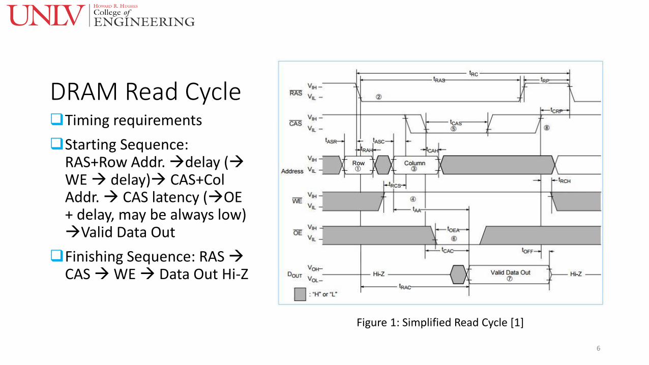
Figure 1: Simplified Read Cycle [1]
DRAM Read Cycle Timing requirements
Starting Sequence: RAS+Row Addr. delay ( WE delay) CAS+Col Addr. CAS latency (OE + delay, may be always low) Valid Data Out
Finishing Sequence: RAS CAS WE Data Out Hi-Z
6
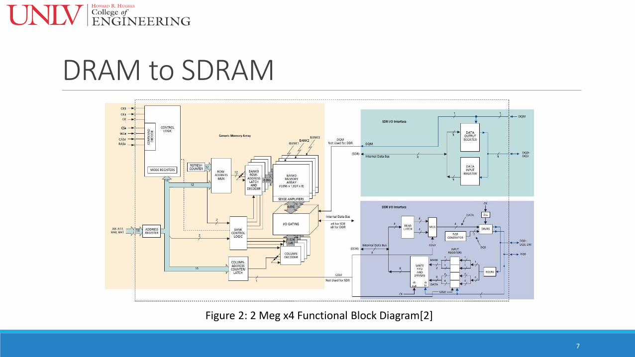
DRAM to SDRAM
7
Figure 2: 2 Meg x4 Functional Block Diagram[2]

Commands in SDRAM
8
Table 1: Truth table for commands in SDRAM [3]
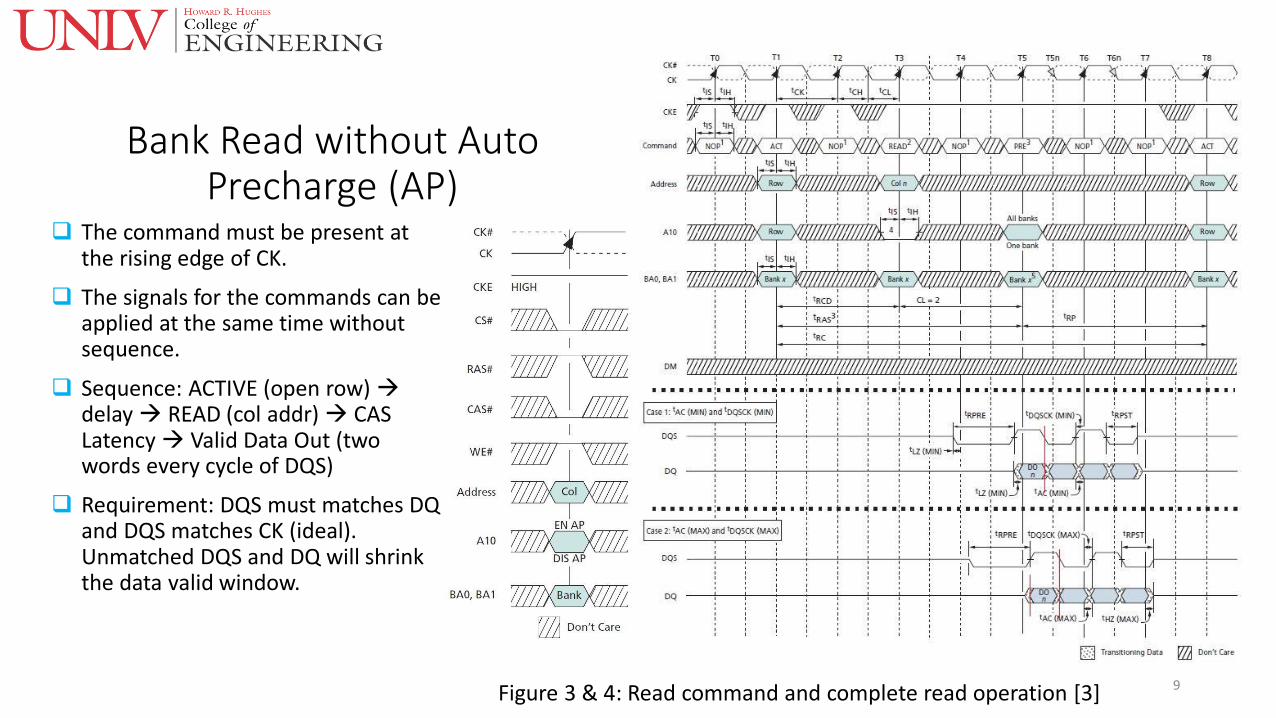
Bank Read without Auto Precharge (AP)
The command must be present at the rising edge of CK.
The signals for the commands can be applied at the same time without sequence.
Sequence: ACTIVE (open row) delay READ (col addr) CAS Latency Valid Data Out (two words every cycle of DQS)
Requirement: DQS must matches DQ and DQS matches CK (ideal). Unmatched DQS and DQ will shrink the data valid window.
9 Figure 3 & 4: Read command and complete read operation [3]

Why is the DLL needed for SDRAM? Synchronize the system clock with DQ and DQS.
Synchronized clock and data will result in maximum data valid window size.
When the edge of DQS is at the center of data valid window: window size cut in half.
Transitioning data region size depends on size of the data word (x8 shown).
10
Figure 5: Data Output Timing and Data Valid Window [3]

Why is the DLL needed for SDRAM? DQ and DQS Synchronization Alternative Methods? Connect DQS directly with system clock? Delay in the input buffer
System clock comes from the memory controller goes into the input buffer.
Delay in the output drivers
Output from the memory goes into output buffer and becomes DQ.
Add a passive (static) delay to model the delay difference between system clock and DQ? Delays in I/O buffer may change with PVT variation.
Variable delays insertion based on the delay difference SMD (Synchronous mirror delay)
PLL (Phase-Locked Loop)
DLL (Delay-Locked Loop)
11

All-Digital DLL Easy to design Discrete delay line
All digital components
Good portability Standard-sized static logic gates
Stable over time Low jitter
Simple linear transfer function Loop filter is a simple counter or shift register
DQS = 0 (external clock) + tD1 + tD + tD2
tD = KF * KDL where KF is an integer ranging from 0 to the number of delay
stages and KDL is the unit delay for each delay element.
12
Figure 6: Digital DLL Block Diagram [4]

Basic Digital DLL Components Phase Detector
Delay insertion Variable delay line (DL) with multiple stages of delay elements Delay elements
Delay stage selector Shift register (SR)
Counter
Input and Output buffer replica
13

DLL Operation DQS = 0 (external clock) + tD1 + tD + tD2
Clk_in: External clock + D1
Clk_out: Clk_in + tD and DQS = Clk_out + D2
Fed_clk: Clk_out + D1’ + D2’ = Clk_in + tD + D1’ + D2’
D1’ + D2’: Feedback delay replica to model the total delays tD1 + tD2
Phase Detector (PD) detects the phase difference between Clk_in and Fed_clk and reports leading or lagging.
SR or counter to increase or decrease the delay in the delay line until Clk_in = Fed_clk (PD in lock). When the clocks are locked, PD will output 0 and the SR will stop shifting to keep the current outputs.
Clk_in = Fed_clk = Clk_in + tD + D1’ + D2’ = 0 tD = 0 – (D1’ + D2’), tD > 0 = N*TCK – (D1’ + D2’)
If TD1’ + TD2’ = TD1 + TD2 , DQS = N*TCK - (TD1’ + TD2’) + TD1 + TD2 = N*TCK.
14
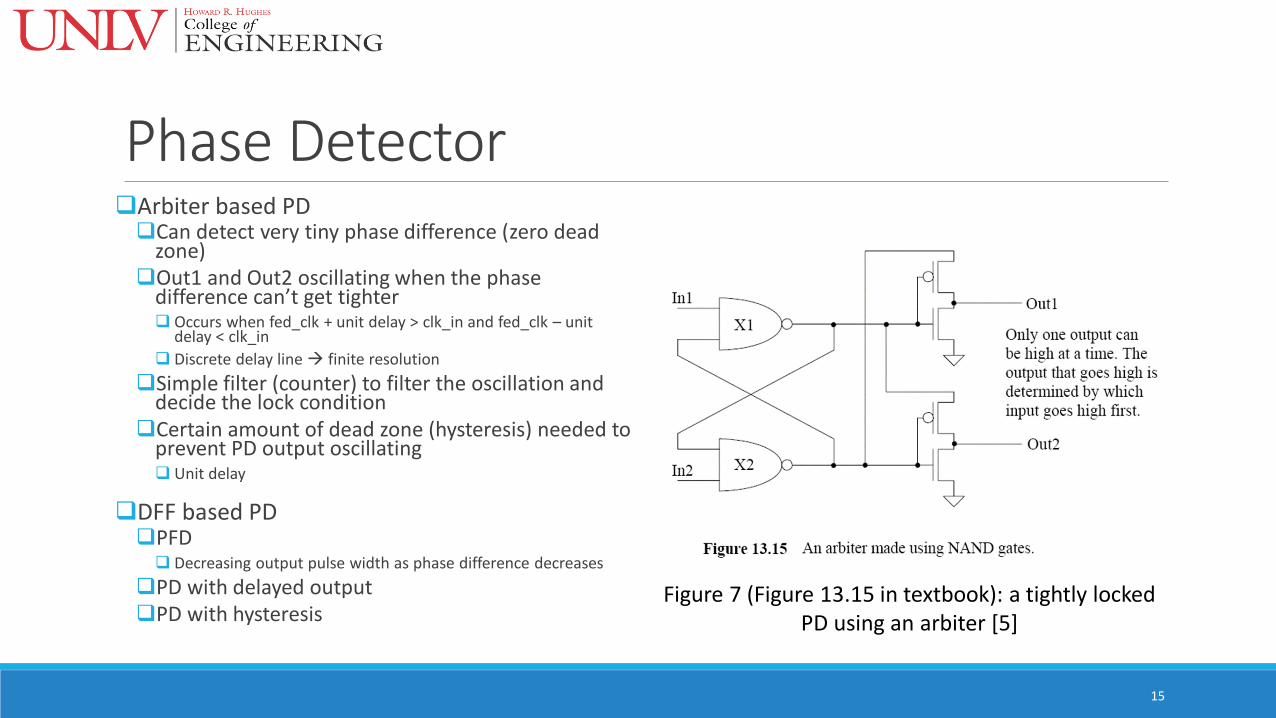
Phase Detector Arbiter based PD Can detect very tiny phase difference (zero dead
zone) Out1 and Out2 oscillating when the phase
difference can’t get tighter Occurs when fed_clk + unit delay > clk_in and fed_clk – unit
delay < clk_in
Discrete delay line finite resolution
Simple filter (counter) to filter the oscillation and decide the lock condition
Certain amount of dead zone (hysteresis) needed to prevent PD output oscillating Unit delay
DFF based PD PFD Decreasing output pulse width as phase difference decreases
PD with delayed output PD with hysteresis
15
Figure 7 (Figure 13.15 in textbook): a tightly locked PD using an arbiter [5]

DFF Based Phase Detector
16
The PD topology shown in Figure 8 will only output once in two clock cycles to give enough time for the SR to adjust the delay.
Potential false lock when the phase difference in time is within (½ *tclk_in – unit delay) to ½ *tclk_in (simulation shown next slide).
The PD topology shown in Figure 9 has the potential metastability that both Out1 and Out2 are high when phase difference is π.
The PD will lock when Φ1 is within Φ2 ± ½*tD. Φ1 > Φ2 + ½*tD: Out1 high; Φ2 > Φ1 + ½*tD
or Φ1 < Φ2 – ½*tD, Out2 high Solution: combine the two topologies and
obtain a PD without false lock and with clocked output.
Figure 8: PD with delayed and clocked output [6]
Figure 9: PD with hysteresis of ½ *tD [7]

False Lock in PD with Delayed Output
17
Figure 10: Schematics and simulation of false lock
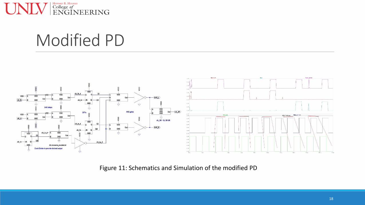
Modified PD
18
Figure 11: Schematics and Simulation of the modified PD

Shift Register and Delay line
19
Figure 13: Bidirectional Shift Registers [8]
Figure 12: Shift register and delay insertion [6]
The delay elements in Figure 12 are 2 NAND gates.
Coarse Delay elements in digital DLL can be almost any digital logics with finite delays. Inverter based NAND + inverter (AND) NAND based
Smaller unit delay higher resolution Shift Register with set and clear
Set certain DFF (Qi) to high to set the point of entry into the delay line
Only one Q will be high at a time Fast-locking DLL

Delay Line Design
20
NAND-NAND delay stage tPLH = tPHL 50% duty cycle Average of 76 ps delay for the number of stages
ranging from 2 to 9. Minimum number of stages is 2 Clk_in goes into the delay line from a NAND gate with the SR output.
Output of the delay line is the delayed and inverted clk_in.
A NAND can be used at the end of delay line to invert the output and remain 50% duty cycles.
Skew in output caused by different inputs (changing) When the clk_in comes into the delay stage from different inputs
(e.g., clk_in to A and NAND_out to B), the final output will have a duty cycle > 50% or < 50%.
Use the same inputs for delayed clk_in in the delay stage path
The output using input B has a larger delay by 8 ps.
Input A is used for delayed clk_in across the delay line.
Clk_in goes into the entry point must use input B to obtain 50% duty cycle.
Figure 14 (Figure 18.15): skew in NAND output [5]
Figure 15: Simulation of 9-stage delay line

Input and Output Buffer Replica Modeling of the input driver and output driver in practical SDRAM design can be difficult since they are complicated. Copy the exact same design Matching delay over PVT variation
Larger layout area
To simplify the design, a simple self-biased differential amplifier from the textbook is used for input buffer.
For output buffer, even number of inverters is used.
Delay Replica contains the exact same designs of input buffer and output buffer.
21
Figure 16 (Figure 18.23): input buffer with logic level outputs [5]

A 550 MHz Digital DLL Design
22
Figure 17: Schematics of a 550 MHz 25 stages Digital DLL SIMULATION

A 550 MHz Digital DLL Design
23
Figure 18: Simulation of the DLL design

To Improve Performance… Duty cycle corrector Ensure the output clock has 50 % duty cycle even when reference external clock doesn’t have 50% duty cycle.
Fine delay line Smaller unit delay than coarse delay line
Total delay must greater or equal to the unit delay of the coarse delay line
Higher resolution locks the external clock tighter
Increasing locking time May be used at the same time with coarse delay line
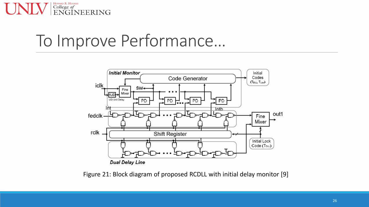
Fast-Locking DLL (Initial delay monitor) Use multiple phase comparator to measure the initial phase difference between the external clock and output
clock.
Using the measured phase, set the corresponding initial point of entry into the delay line so the clocks are almost in phase which saves the time for coarse delay shifting.
24

To Improve Performance…
25
Figure 19: Conventional Duty Cycle Corrector [9] Figure 20: Alternative Fine Delay Elements [10]
To Improve Performance…
26
Figure 21: Block diagram of proposed RCDLL with initial delay monitor [9]
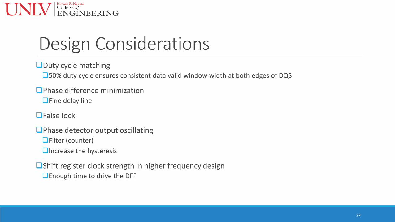
Design Considerations Duty cycle matching 50% duty cycle ensures consistent data valid window width at both edges of DQS
Phase difference minimization Fine delay line
False lock
Phase detector output oscillating Filter (counter)
Increase the hysteresis
Shift register clock strength in higher frequency design Enough time to drive the DFF
27

References [1] “Allocations Note - Understanding DRAM Operation”, IBM Corporation, 1996
[2] “Technical Note – General DDR SDRAM Functionality”, TN-46-05, Micron Technology, Inc., 2001
[3] “512Mb: x4, x8, x16 DDR SDRAM Features”, Datasheet, Micron Technology, Inc., 2000
[4] Becker, Eric A. (2008). DESIGN OF AN INTEGRATED HALF-CYCLE DELAY LINE DUTY CYCLE
CORRECTOR DELAY-LOCKED LOOP (Master’s thesis). Retrieved from cmosedu.com
[5] R. Jacob Baker, “CMOS Circuit Design, Layout, and Simulation,” 3rd ed. Wiley-IEEE Press, 2010
[6] Feng Lin; Miller, J.; Schoenfeld, A.; Ma, M.; Baker, R.J., "A register-controlled symmetrical DLL for double-data-rate DRAM," in Solid-State Circuits, IEEE Journal of , vol.34, no.4, pp.565-568, Apr 1999
[7] Booth, Eric R. (2006). WIDE RANGE, LOW JITTER DELAY-LOCKED LOOP USING A GRADUATED
DIGITAL DELAY LINE AND PHASE INTERPOLATOR (Master’s thesis). Retrieved from cmosedu.com
[8] Allan Li. “Bidirectional Shift Registers”, tutorial, Retrieved from http://www.ee.usyd.edu.au/tutorials/digital_tutorial/part2/hpage.html, Accessed on November 17, 2015.
[9] Shin, Dongsuk; Cho, Joo-Hwan; Young-Jung Choi; Byoung-Tae Chung, "Frequency-independent fast-lock register-controlled DLL with wide-range duty cycle adjuster," in SOC Conference (SOCC), 2010 IEEE International , vol., no., pp.79-82, 27-29 Sept. 2010
[10] Tuvia Liran and Ran Ginosar, “All-Digital DLL Architecture and Applications”, Technical Report, September 2005
28

QUESTIONS?
29


