• Portable Audio Devices• Supports 8-kHz to 192-kHz Sample Rates• White goods• Mono Class-D BTL Speaker Driver (2 W Into• Portable Navigation Devices4 Ω or 1.7 W Into 8 Ω)
• Mono Headphone Driver1.3 Description• Two Single-Ended Inputs With Output Mixing
and Level ControlThe TAS2521 is a low power digital input speaker
• Embedded Power-on-Resetamp with support for 24-bit digital I2S data mono
• Integrated LDO playback.• Built-in Digital Audio Processing Blocks With
In addition to driving a speaker amp upto 4-Ω, theUser-Programmable Biquad Filtersdevice also features a mono headphone driver and a• Integrated PLL Used for Programmable Digitalfully programmable miniDSP for signal processing.Audio ProcessorThe digital audio data format is programmable to• I2S, Left-Justified, Right-Justified, DSP, andwork with popular audio standard protocols (I2S,TDM Audio Interfacesleft/right-justified) in master, slave, DSP and TDM• I2C and SPI control with auto-incrementmodes. The fully programmable miniDSP can support• Full Power-Down Controlseveral functions such equalization for audio, multi-• Power Supplies:band DRC, tone generation and several other user– Analog: 1.5 V–1.95 Vdefined functions. An on-chip PLL provides the high-– Digital Core: 1.65 V–1.95 Vspeed clock needed by the digital signal-processing– Digital I/O: 1.1 V–3.6 Vblock. The volume level can be controlled by register
– Class-D: 2.7 V–5.5 V (SPKVDD ≥ AVDD) control. The audio functions are controlled using the• 24-Pin QFN Package (4mm × 4mm) I2C™ serial bus or SPI bus. The device includes an
on-board LDO that runs off the speaker power supplyto handle all internal device analog and digital powerneeds. The included POR as power-on-resetcircuitreliably resets the device into its default state so noexternal reset is required at normal usage; however,the device does have a reset pin for more complexsystem initialization needs. The device also includestwo analog inputs for mixing and muxing in bothspeaker and headphone analog paths.
1
Please be aware that an important notice concerning availability, standard warranty, and use in critical applications ofTexas Instruments semiconductor products and disclaimers thereto appears at the end of this data sheet.
SLAS687A –FEBRUARY 2013–REVISED FEBRUARY 2013 www.ti.com
This integrated circuit can be damaged by ESD. Texas Instruments recommends that all integrated circuits be handled withappropriate precautions. Failure to observe proper handling and installation procedures can cause damage.
ESD damage can range from subtle performance degradation to complete device failure. Precision integrated circuits may be moresusceptible to damage because very small parametric changes could cause the device not to meet its published specifications.
Figure 1-1. Simplified Block Diagram
NOTEThis data manual is designed using PDF document-viewing features that allow quick accessto information. For example, performing a global search on "page 0 / register 27" producesall references to this page and register in a list. This makes is easy to traverse the list andfind all information related to a page and register. Note that the search string must be of theindicated format. Also, this document includes document hyperlinks to allow the user toquickly find a document reference. To come back to the original page, click the green leftarrow near the PDF page number at the bottom of the file. The hot-key for this function is alt-left arrow on the keyboard. Another way to find information quickly is to use the PDFbookmarks.
SLAS687A –FEBRUARY 2013–REVISED FEBRUARY 2013 www.ti.com
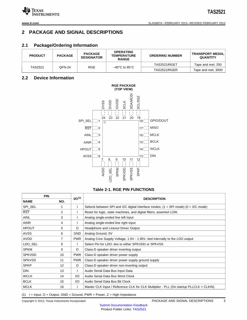
Table 2-1. RGE PIN FUNCTIONS (continued)
PINI/O (1) DESCRIPTION
NAME NO.
MISO 17 O SPI Serial Data Output
GPIO/DOUT 18 I/O/Z GPIO / Audio Serial Bus Output
SCL/SSZ 19 I Either I2C Input Serial Clock or SPI Chip Select Signal depending on SPI_SEL state
SDA/MOSI 20 I Either I2C Serial Data Input or SPI Serial Data Input depending on SPI_SEL state.
SCLK 21 I Serial clock for SPI interface
IOVDD 22 PWR I/O Power Supply, 1.1V - 3.6V
DVDD 23 PWR Digital Power Supply, 1.65V - 1.95V
DVSS 24 GND Digital Ground, 0V
3 ELECTRICAL SPECIFICATIONS
3.1 Absolute Maximum Ratingsover operating free-air temperature range (unless otherwise noted) (1)
VALUEUNIT
MIN MAX
AVDD to AVSS –0.3 2.2 V
DVDD to DVSS –0.3 2.2 V
SPKVDD to SPKVSS –0.3 6 V
IOVDD to IOVSS –0.3 3.9 V
Digital input voltage IOVSS – 0.3 IOVDD + 0.3 V
Analog input voltage AVSS – 0.3 AVDD + 0.3 V
Operating temperature range –40 85 °C
Storage temperature range –55 150 °C
Junction temperature (TJ Max) 105 °C
QFN Power dissipation(with thermal pad soldered to board) (TJ Max – TA) / θJA W
(1) Stresses beyond those listed under Absolute Maximum Ratings may cause permanent damage to the device. These are stress ratingsonly, and functional operation of the device at these or any other conditions beyond those indicated under Recommended OperatingConditions is not implied. Exposure to absolute-maximum-rated conditions for extended periods may affect device reliability.
(1) To minimize battery-current leakage, the SPKVDD voltage level should not be below the AVDD voltage level.(2) All grounds on board are tied together, so they should not differ in voltage by more than 0.2 V maximum for any combination of ground
signals. By use of a wide trace or ground plane, ensure a low-impedance connection between AVSS and DVSS.(3) The maximum input frequency should be 50 MHz for any digital pin used as a general-purpose clock.
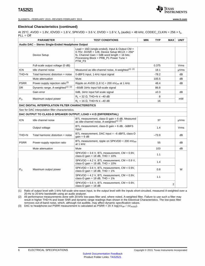
THD+N Total harmonic distortion + noise 0-dBFS input, 1-kHz input signal -78.2 dB
Mute attenuation Mute 103.7 dB
PSRR Power-supply rejection ratio (3) Ripple on AVDD (1.8 V) = 200 mVPP at 1 kHz 47.2 dB
DR Dynamic range, A-weighted (1) (2) –60dB 1kHz input full-scale signal 88.1
Gain error 0dB, 1kHz input full scale signal ±0.3 dB
RL = 32 Ω, THD+N ≤ –40 dB 11PO Maximum output power mW
RL = 16 Ω, THD+N ≤ –40 dB 18
(1) Ratio of output level with 1-kHz full-scale sine-wave input, to the output level with the inputs short-circuited, measured A-weighted over a20-Hz to 20-kHz bandwidth using an audio analyzer.
(2) All performance measurements done with 20-kHz low-pass filter and, where noted, A-weighted filter. Failure to use such a filter mayresult in higher THD+N and lower SNR and dynamic range readings than shown in the Electrical Characteristics. The low-pass filterremoves out-of-band noise, which, although not audible, may affect dynamic specification values.
(3) DAC to headphone-out PSRR measurement is calculated as PSRR = 20 X log(∆VHP / ∆VAVDD).
BTL measurement, class-D gain = 6 dB, -3dBFSOutput voltage 1.4 Vrmsinput
BTL measurement, DAC input = –6 dBFS, class-DTHD+N Total harmonic distortion + noise –73.9 dBgain = 6 dB
BTL measurement, ripple on SPKVDD = 200 mVPPPSRR Power-supply rejection ratio 55 dBat 1 kHz
Mute attenuation Mute 103 dB
SPKVDD = 3.6 V, BTL measurement, CM = 0.9V, 1.1class-D gain = 18 dB, THD = 10%
SPKVDD = 4.2 V, BTL measurement, CM = 0.9 V, 1.4class-D gain = 18 dB, THD = 10%
SPKVDD = 3.6 V, BTL measurement, CM = 0.9V,PO Maximum output power 0.8 Wclass-D gain = 18 dB, THD = 1%
SPKVDD = 4.2 V, BTL measurement, CM = 0.9V, 1.1class-D gain = 18 dB, THD = 1%
SPKVDD = 5.5 V, BTL measurement, CM = 0.9V, 2class-D gain = 18 dB
(1) Ratio of output level with 1-kHz full-scale sine-wave input, to the output level with the inputs short-circuited, measured A-weighted over a20-Hz to 20-kHz bandwidth using an audio analyzer.
(2) All performance measurements done with 20-kHz low-pass filter and, where noted, A-weighted filter. Failure to use such a filter mayresult in higher THD+N and lower SNR and dynamic range readings than shown in the Electrical Characteristics. The low-pass filterremoves out-of-band noise, which, although not audible, may affect dynamic specification values.
(3) DAC to headphone-out PSRR measurement is calculated as PSRR = 20 X log(∆VHP / ∆VAVDD).
BTL measurement, class-D gain = 6 dB, -3dBFSOutput voltage 1.4 Vrmsinput
BTL measurement, DAC input = –6 dBFS, class-DTHD+N Total harmonic distortion + noise –73.6 dBgain = 6 dB
SPKVDD = 3.6 V, BTL measurement, CM = 0.9V, 0.7class-D gain = 18 dB, THD = 10%
SPKVDD = 4.2 V, BTL measurement, CM = 0.9V, 1class-D gain = 18 dB, THD = 10%
SPKVDD = 5.5 V, BTL measurement, CM = 0.9V, 1.7class-D gain = 18 dB, THD = 10%PO Maximum output power W
SPKVDD = 3.6 V, BTL measurement, CM = 0.9V, 0.5class-D gain = 18 dB, THD = 1%
SPKVDD = 4.2 V, BTL measurement, CM = 0.9V, 0.8class-D gain = 18 dB, THD = 1%
SPKVDD = 5.5 V, BTL measurement, CM = 0.9V, 1.3class-D gain = 18 dB, THD = 1%
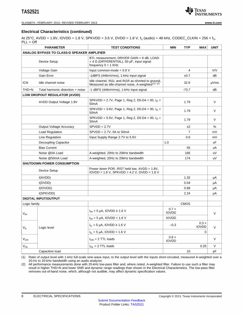
ANALOG BYPASS TO HEADPHONE AMPLIFIER
AC-COUPLED LOAD = 16 Ω (SINGLE-ENDED),Device Setup DRIVER GAIN = 0 dB, Input and output common-
mode = 0.9 V, input signal frequency fi = 1kHz
Voltage Gain Input common-mode = 0.9 V 1 V/V
Gain Error -1dBFS (446mVrms), 1-kHz input signal ±0.8 dB
Idle channel, IN1L and IN1R ac-shorted to ground,ICN Idle channel noise 10.2 μVmsMeasured as idle-channel noise, A-weighted (1) (2)
THD+N Total harmonic distortion + noise -1 dBFS (446mVrms), 1-kHz input signal -80.4 dB
(1) Ratio of output level with 1-kHz full-scale sine-wave input, to the output level with the inputs short-circuited, measured A-weighted over a20-Hz to 20-kHz bandwidth using an audio analyzer.
(2) All performance measurements done with 20-kHz low-pass filter and, where noted, A-weighted filter. Failure to use such a filter mayresult in higher THD+N and lower SNR and dynamic range readings than shown in the Electrical Characteristics. The low-pass filterremoves out-of-band noise, which, although not audible, may affect dynamic specification values.
www.ti.com SLAS687A –FEBRUARY 2013–REVISED FEBRUARY 2013
5.2 Circuit Configuration with Internal LDO
Figure 5-2. Application Schematics for LDO
5.3 Device Connections
5.3.1 Digital Pins
Only a small number of digital pins are dedicated to a single function; whenever possible, the digital pinshave a default function, and also can be reprogrammed to cover alternative functions for variousapplications.
The fixed-function pins are RST LDO_SEL and the SPI_SEL pin, which are HW control pins. Dependingon the state of SPI_SEL, the two control-bus pins SCL/SSZ and SDA/MOSI are configured for either I2Cor SPI protocol.
Other digital IO pins can be configured for various functions via register control. An overview of availablefunctionality is given in Section 5.3.3.
5.3.2 Analog Pins
Analog functions can also be configured to a large degree. For minimum power consumption, analogblocks are powered down by default. The blocks can be powered up with fine granularity according to theapplication needs.
SLAS687A –FEBRUARY 2013–REVISED FEBRUARY 2013 www.ti.com
5.3.3 Multifunction Pins
Table 5-1 shows the possible allocation of pins for specific functions. The PLL input, for example, can beprogrammed to be any of 4 pins (MCLK, BCLK, DIN, GPIO).
Table 5-1. Multifunction Pin Assignments
1 2 3 4 5 6 7
Pin Function MCLK BCLK WCLK DIN GPIO SCLK MISO/DOUT
A PLL Input S (1) S (2) E S (3)
B Codec Clock Input S (1),D (4) S (2) S (3)
C I2S BCLK input S (2),D
D I2S BCLK output E (5)
E I2S WCLK input E, D
F I2S WCLK output E
G I2S DIN E, D
H I2S DOUT E
I General Purpose Output I E
I General Purpose Output II E
J General Purpose Input I E
J General Purpose Input II E
J General Purpose Input III E
K INT1 output E E
L INT2 output E E
M Secondary I2S BCLK input E E
N Secondary I2S WCLK input E E
O Secondary I2S DIN E E
P Secondary I2S BCLK OUT E E
Q Secondary I2S WCLK OUT E E
R Secondary I2S DOUT E
S Aux Clock Output E E
(1) S(1): The MCLK pin can drive the PLL and Codec Clock inputs simultaneously.(2) S(2): The BCLK pin can drive the PLL and Codec Clock and audio interface bit clock inputs simultaneously.(3) S(3): The GPIO/DOUT pin can drive the PLL and Codec Clock inputs simultaneously.(4) D: Default Function(5) E: The pin is exclusively used for this function, no other function can be implemented with the same pin. (If GPIO/DOUT has been
allocated for General Purpose Output, it cannot be used as the INT1 output at the same time.)
5.4 Audio Analog I/O
The TAS2521 features a mono audio DAC. It supports a wide range of analog interfaces to supportdifferent headsets such as 16-Ω to 200-Ω impedance and analog line outputs. TheTAS2521 can drive aspeaker upto 4-Ω impedance.
5.5 Analog Signals
The TAS2521 analog signals consist of:• Analog inputs AINR and AINL, which can be used to pass-through or mix analog signals to output
stages• Analog outputs class-D speaker driver and headphone/lineout driver providing output capability for the
www.ti.com SLAS687A –FEBRUARY 2013–REVISED FEBRUARY 2013
5.5.1 Analog Inputs AINL and AINR
AINL (pin 3 or C2) and AINR (pin 4 or B2) are inputs to Mixer P and Mixer M along with the DAC output.Also AINL and AINR can be configured inputs to HP driver. Page1 / register 12 provides control signals fordetermining the signals routed through Mixer P, Mixer M and HP driver. Input of Mixer P can beattenuated by Page1 / register 24, input of Mixer M can be attenuated by Page1 / register 25 and input ofHP driver can be attenuated by Page1 / register 22. Also AINL and AINR can be configured to a monauraldifferential input with use Mixer P and Mixer M by Page1 / register 12 setting.
For more detailed information see the TAS2521 Application Reference Guide (SLAU456).
5.6 Audio DAC and Audio Analog Outputs
The mono audio DAC consists of a digital audio processing block, a digital interpolation filter, a digitaldelta-sigma modulator, and an analog reconstruction filter. The high oversampling ratio (normally DOSR isbetween 32 and 128) exhibits good dynamic range by ensuring that the quantization noise generatedwithin the delta-sigma modulator stays outside of the audio frequency band. Audio analog outputs includemono headphone and lineout and mono class-D speaker outputs. Because the TAS2521 contains a monoDAC, it inputs the mono data from the left channel, the right channel, or a mix of the left and rightchannels as [(L + R) ÷ 2], selected by page 0, register 63, bits D5–D4.
For more detailed information see the TAS2521 Application Reference Guide (SLAU456).
5.6.1 DAC
The TAS2521 mono audio DAC supports data rates from 8 kHz to 192 kHz. The audio channel of themono DAC consists of a signal-processing engine with fixed processing blocks, a programmable miniDSP,a digital interpolation filter, multibit digital delta-sigma modulator, and an analog reconstruction filter. TheDAC is designed to provide enhanced performance at low sampling rates through increased oversamplingand image filtering, thereby keeping quantization noise generated within the delta-sigma modulator andobserved in the signal images strongly suppressed within the audio band to beyond 20 kHz. To handlemultiple input rates and optimize power dissipation and performance, the TAS2521 allows the systemdesigner to program the oversampling rates over a wide range from 1 to 1024 by configuring page 0,register 13 and page 0 / register 14. The system designer can choose higher oversampling ratios for lowerinput data rates and lower oversampling ratios for higher input data rates.
The TAS2521 DAC channel includes a built-in digital interpolation filter to generate oversampled data forthe delta-sigma modulator. The interpolation filter can be chosen from three different types, depending onrequired frequency response, group delay, and sampling rate.
The DAC path of the TAS2521 features many options for signal conditioning and signal routing:• Digital volume control with a range of -63.5 to +24dB• Mute function
In addition to the standard set of DAC features the TAS2521 also offers the following special features:• Digital auto mute• Adaptive filter mode
5.6.1.1 DAC Processing Blocks — Overview
The TAS2521 implements signal-processing capabilities and interpolation filtering via processing blocks.These fixed processing blocks give users the choice of how much and what type of signal processing theymay use and which interpolation filter is applied.
The choices among these processing blocks allows the system designer to balance power conservationand signal-processing flexibility. Table 5-2 gives an overview of all available processing blocks of the DACchannel and their properties. The resource-class column gives an approximate indication of powerconsumption for the digital (DVDD) supply; however, based on the out-of-band noise spectrum, the analogpower consumption of the drivers (AVDD) may differ.
SLAS687A –FEBRUARY 2013–REVISED FEBRUARY 2013 www.ti.com
The signal-processing blocks available are:• First-order IIR• Scalable number of biquad filters
The processing blocks are tuned for common cases and can achieve high image rejection or low groupdelay in combination with various signal-processing effects such as audio effects and frequency shaping.The available first-order IIR and biquad filters have fully user-programmable coefficients.
Processing First-Order Number of ResourceInterpolation Filter ChannelBlock No. IIR Available Biquads Class
PRB_P1 A Mono Yes 6 6
PRB_P2 A Mono No 3 4
PRB_P3 B Mono Yes 6 4
For more detailed information see the TAS2521 Application Reference Guide (SLAU456).
5.6.2 Digital Mixing and Routing
The TAS2521 has four digital mixing blocks. Each mixer can provide either mixing or multiplexing of thedigital audio data. The first mixer/multiplexer can be used to select input data for the mono DAC from leftchannel, right channel, or (left channel + right channel) / 2 mixing. This digital routing can be configured bywriting to page 0, register 63, bits D5–D4.
5.6.3 Analog Audio Routing
The TAS2521 has the capability to route the DAC output to either the headphone or the speaker output. Ifdesirable, both output drivers can be operated at the same time while playing at different volume levels.The TAS2521 provides various digital routing capabilities, allowing digital mixing or even channelswapping in the digital domain. All analog outputs other than the selected ones can be powered down foroptimal power consumption.
For more detailed information see the TAS2521 Application Reference Guide (SLAU456).
5.6.4 5V LDO
The TAS2521 has a built-in LDO which can generate the analog supply (AVDD) also the digital supply(DVDD) from input voltage range of 2.7 V to 5.5 V with high PSRR. If combined power supply current is50 mA or less, then this LDO can deliver power to both analog and digital power supplies. If the onlyspeaker power supply is present and LDO Select pin is enabled, the LDO can power up without requiringother supplies. This LDO requires a minimum dropout voltage of 300 mV and can support load currents upto 50 mA. For stability reasons the LDO requires a minimum decoupling capacitor of 1 µF (±50%) on theanalog supply (AVDD) pin and the digital supply (DVDD) pin. If use this LDO output voltage for the digitalsupply (DVDD) pin, the analog supply (AVDD) pin connected to the digital supply (DVDD) externally isrequired.
The LDO is by default powered down for low sleep mode currents and can be enabled driving theLDO_SELECT pin to SPKVDD (Speaker power supply). When the LDO is disabled the AVDD pin is tri-stated and the device AVDD needs to be powered using external supply. In that case the DVDD pin isalso tri-stated and the device DVDD needs to be powered using external supply. The output voltage of thisLDO can be adjusted to a few different values as given in the Table 5-3.
www.ti.com SLAS687A –FEBRUARY 2013–REVISED FEBRUARY 2013
Table 5-3. AVDD LDO Settings
Page-1, Register 2, D(5:4) LDO Output
00 1.8 V
01 1.6 V
10 1.7 V
00 1.5 V
For more detailed information see the TAS2521 Application Reference Guide (SLAU456).
5.6.5 POR
TAS2521 has a POR (Power On Reset) function. This function insures that all registers are automaticallyset to defaults when a proper power up sequence is executed.
For more detailed information see the TAS2521 Application Reference Guide (SLAU456).
5.6.6 CLOCK Generation and PLL
The TAS2521 supports a wide range of options for generating clocks for the DAC sections as well asinterface and other control blocks. The clocks for the DAC require a source reference clock. This clock canbe provided on a variety of device pins, such as the MCLK, BCLK, or GPIO pins. The source referenceclock for the codec can be chosen by programming the CODEC_CLKIN value on page 0, register 4, bitsD1–D0. The CODEC_CLKIN can then be routed through highly-flexible clock dividers shown in togenerate the various clocks required for the DAC and the miniDSP section. In the event that the desiredaudio clocks cannot be generated from the reference clocks on MCLK, BCLK, or GPIO, the TAS2521 alsoprovides the option of using the on-chip PLL which supports a wide range of fractional multiplicationvalues to generate the required clocks. Starting from CODEC_CLKIN, the TAS2521 provides severalprogrammable clock dividers to help achieve a variety of sampling rates for the DAC and clocks for theminiDSP sections.
For more detailed information see the TAS2521 Application Reference Guide (SLAU456).
5.6.7 Digital Audio and Control Interface
5.6.7.1 Digital Audio Interface
Audio data is transferred between the host processor and the TAS2521 via the digital audio data serialinterface, or audio bus. The audio bus on this device is flexible, including left- or right-justified dataoptions, support for I2S or PCM protocols, programmable data-length options, a TDM mode formultichannel operation, flexible master/slave configurability for each bus clock line, and the ability tocommunicate with multiple devices within a system directly.
The audio bus of the TAS2521 can be configured for left- or right-justified, I2S, DSP, or TDM modes ofoperation, where communication with standard telephony PCM interfaces is supported within the TDMmode. These modes are all MSB-first, with data width programmable as 16, 20, 24, or 32 bits byconfiguring page 0, register 27, bits D5–D4. In addition, the word clock and bit clock can be independentlyconfigured in either master or slave mode for flexible connectivity to a wide variety of processors. Theword clock is used to define the beginning of a frame, and may be programmed as either a pulse or asquare-wave signal. The frequency of this clock corresponds to the maximum of the selected DACsampling frequencies.
For more detailed information see the TAS2521 Application Reference Guide (SLAU456).
5.6.7.2 Control Interface
The TAS2521 control interface supports SPI or I2C communication protocols, with the protocol selectableusing the SPI_SEL pin. For SPI, SPI_SEL should be tied high; for I2C, SPI_SEL should be tied low. It isnot recommended to change the state of SPI_SEL during device operation.
SLAS687A –FEBRUARY 2013–REVISED FEBRUARY 2013 www.ti.com
5.6.7.2.1 I2C Control Mode
The TAS2521 supports the I2C control protocol, and will respond to the I2C address of 0011 000. I2C is atwo-wire, open-drain interface supporting multiple devices and masters on a single bus. Devices on theI2C bus only drive the bus lines LOW by connecting them to ground; they never drive the bus lines HIGH.Instead, the bus wires are pulled HIGH by pullup resistors, so the bus wires are HIGH when no device isdriving them LOW. This way, two devices cannot conflict; if two devices drive the bus simultaneously,there is no driver contention.
5.6.7.2.2 SPI Digital Interface
In the SPI control mode,the TAS2521 uses the pins SCL/SSZ=SSZ, SCLK=SCLK, MISO=MISO,SDA/MOSI=MOSI as a standard SPI port with clock polarity setting of 0 (typical microprocessor SPIcontrol bit CPOL = 0). The SPI port allows full-duplex, synchronous, serial communication between a hostprocessor (the master) and peripheral devices (slaves). The SPI master (in this case, the host processor)generates the synchronizing clock (driven onto SCLK) and initiates transmissions. The SPI slave devices(such as the TAS2521) depend on a master to start and synchronize transmissions. A transmission beginswhen initiated by an SPI master.The byte from the SPI master begins shifting in on the slave MOSI pinunder the control of the master serial clock(driven onto SCLK). As the byte shifts in on the MOSI pin, abyte shifts out on the MISO pin to the master shif tregister.
For more detailed information see the TAS2521 Application Reference Guide (SLAU456).
5.6.7.3 Power Supply
The TAS2521 integrates a large amount of digital and analog functionality, and each of these blocks canbe powered separately to enable the system to select appropriate power supplies for desired performanceand power consumption. The device has separate power domains for digital IO, digital core, analog core,analog input, headphone driver, and speaker drivers. If desired, all of the supplies (except for the suppliesfor speaker drivers, which can directly connect to the battery) can be connected together and be suppliedfrom one source in the range of 1.65 to 1.95V. Individually, the IOVDD voltage can be supplied in therange of 1.1V to 3.6V. For improved power efficiency, the digital core power supply can range from 1.26Vto 1.95V. The analog core supply can either be derived from the internal LDO accepting an SPKVDDvoltage in the range of 2.7V to 5.5V, or the AVDD pin can directly be driven with a voltage in the range of1.5V to 1.95V. The speaker driver voltages (SPKVDD) can range from 2.7V to 5.5V.
For more detailed information see the TAS2521 Application Reference Guide (SLAU456).
5.6.7.4 Device Special Functions
• Interrupt generation• Flexible pin multiplexing
For more detailed information see the TAS2521 Application Reference Guide (SLAU456).
5.6.7.5 miniDSP
The TAS2521 features a miniDSP core which is tightly coupled to the DAC. The fully programmablealgorithms for the miniDSP must be loaded into the device after power up. The miniDSP has direct accessto the digital audio stream, offering the possibility for advanced, very low-group-delay DSP algorithms. TheminiDSP has 512 programmable instructions, 896 data memory locations, and 512 programmablecoefficients (in the adaptive mode, each bank has 256 programmable coefficients).
www.ti.com SLAS687A –FEBRUARY 2013–REVISED FEBRUARY 2013
5.6.7.5.1 Software
Software development for the TAS2521 is supported through TI's comprehensive PurePath™ Studiosoftware development environment, a powerful, easy-to-use tool designed specifically to simplify softwaredevelopment on Texas Instruments miniDSP audio platforms. The graphical development environmentconsists of a library of common audio functions that can be dragged and dropped into an audio signal flowand graphically connected together. The DSP code can then be assembled from the graphical signal flowwith the click of a mouse. See the TAS2521 product folder on www.ti.com to learn more about PurePathStudio and the latest status on available, ready-to-use DSP algorithms.
NOTE: Page numbers for previous revisions may differ from page numbers in the current version.
Changes from Original (February 2013) to Revision A Page
• Deleted PO (Max Output power) SPKVDD = 5.5 V, THD = 10% .............................................................. 6• Changed PO (Max Output power) SPKVDD = 5.5 V value From: TYP = 2.1 W To: MAX = 2 W ......................... 6
TAS2521IRGER ACTIVE VQFN RGE 24 3000 RoHS & Green NIPDAU Level-2-260C-1 YEAR -40 to 85 TAS2521
TAS2521IRGET ACTIVE VQFN RGE 24 250 RoHS & Green NIPDAU Level-2-260C-1 YEAR -40 to 85 TAS2521
(1) The marketing status values are defined as follows:ACTIVE: Product device recommended for new designs.LIFEBUY: TI has announced that the device will be discontinued, and a lifetime-buy period is in effect.NRND: Not recommended for new designs. Device is in production to support existing customers, but TI does not recommend using this part in a new design.PREVIEW: Device has been announced but is not in production. Samples may or may not be available.OBSOLETE: TI has discontinued the production of the device.
(2) RoHS: TI defines "RoHS" to mean semiconductor products that are compliant with the current EU RoHS requirements for all 10 RoHS substances, including the requirement that RoHS substancedo not exceed 0.1% by weight in homogeneous materials. Where designed to be soldered at high temperatures, "RoHS" products are suitable for use in specified lead-free processes. TI mayreference these types of products as "Pb-Free".RoHS Exempt: TI defines "RoHS Exempt" to mean products that contain lead but are compliant with EU RoHS pursuant to a specific EU RoHS exemption.Green: TI defines "Green" to mean the content of Chlorine (Cl) and Bromine (Br) based flame retardants meet JS709B low halogen requirements of <=1000ppm threshold. Antimony trioxide basedflame retardants must also meet the <=1000ppm threshold requirement.
(3) MSL, Peak Temp. - The Moisture Sensitivity Level rating according to the JEDEC industry standard classifications, and peak solder temperature.
(4) There may be additional marking, which relates to the logo, the lot trace code information, or the environmental category on the device.
(5) Multiple Device Markings will be inside parentheses. Only one Device Marking contained in parentheses and separated by a "~" will appear on a device. If a line is indented then it is a continuationof the previous line and the two combined represent the entire Device Marking for that device.
(6) Lead finish/Ball material - Orderable Devices may have multiple material finish options. Finish options are separated by a vertical ruled line. Lead finish/Ball material values may wrap to twolines if the finish value exceeds the maximum column width.
Important Information and Disclaimer:The information provided on this page represents TI's knowledge and belief as of the date that it is provided. TI bases its knowledge and belief on informationprovided by third parties, and makes no representation or warranty as to the accuracy of such information. Efforts are underway to better integrate information from third parties. TI has taken andcontinues to take reasonable steps to provide representative and accurate information but may not have conducted destructive testing or chemical analysis on incoming materials and chemicals.TI and TI suppliers consider certain information to be proprietary, and thus CAS numbers and other limited information may not be available for release.
In no event shall TI's liability arising out of such information exceed the total purchase price of the TI part(s) at issue in this document sold by TI to Customer on an annual basis.
Images above are just a representation of the package family, actual package may vary.Refer to the product data sheet for package details.
RGE 24 VQFN - 1 mm max heightPLASTIC QUAD FLATPACK - NO LEAD
4204104/H
NOTES:
1. All linear dimensions are in millimeters. Any dimensions in parenthesis are for reference only. Dimensioning and tolerancing
per ASME Y14.5M.
2. This drawing is subject to change without notice.
3. The package thermal pad must be soldered to the printed circuit board for thermal and mechanical performance.
PACKAGE OUTLINE
www.ti.com
4219016 / A 08/2017
VQFN - 1 mm max height
PLASTIC QUAD FLATPACK- NO LEAD
RGE0024H
A
0.08 C
0.1 C A B
0.05 C
B
SYMM
SYMM
4.1
3.9
4.1
3.9
PIN 1 INDEX AREA
1 MAX
0.05
0.00
SEATING PLANE
C
2X 2.5
2.7±0.1
2X
2.5
20X 0.5
1
6
7
12
13
18
19
24
24X
0.30
0.18
24X
0.48
0.28
(0.2) TYP
PIN 1 ID
(OPTIONAL)
25
NOTES: (continued)
4. This package is designed to be soldered to a thermal pad on the board. For more information, see Texas Instruments
literature number SLUA271 (www.ti.com/lit/slua271).5. Solder mask tolerances between and around signal pads can vary based on board fabrication site.
EXAMPLE BOARD LAYOUT
4219016 / A 08/2017
www.ti.com
VQFN - 1 mm max height
RGE0024H
PLASTIC QUAD FLATPACK- NO LEAD
SYMM
SYMM
LAND PATTERN EXAMPLE
SCALE: 20X
2X
(1.1)
2X(1.1)
(3.825)
(3.825)
( 2.7)
1
6
7 12
13
18
1924
25
24X (0.58)
24X (0.24)
20X (0.5)
(R0.05)
(Ø0.2) VIA
TYP
SOLDER MASK DETAILS
NON SOLDER MASK
DEFINED
(PREFERRED)
SOLDER MASK
DEFINED
0.07 MAX
ALL AROUND
0.07 MIN
ALL AROUND
METAL
SOLDER MASK
OPENING
SOLDER MASK
OPENING
METAL UNDER
SOLDER MASK
NOTES: (continued)
6. Laser cutting apertures with trapezoidal walls and rounded corners may offer better paste release. IPC-7525 may have alternate
design recommendations..
EXAMPLE STENCIL DESIGN
4219016 / A 08/2017
www.ti.com
VQFN - 1 mm max height
RGE0024H
PLASTIC QUAD FLATPACK- NO LEAD
SYMM
SYMM
SOLDER PASTE EXAMPLE
BASED ON 0.125 mm THICK STENCIL
EXPOSED PAD
78% PRINTED COVERAGE BY AREA
SCALE: 20X
(3.825)
(3.825)
(0.694)
TYP
(0.694)
TYP
4X ( 1.188)
1
6
712
13
18
1924
24X (0.24)
24X (0.58)
20X (0.5)
(R0.05) TYP
METAL
TYP
25
IMPORTANT NOTICE AND DISCLAIMER
TI PROVIDES TECHNICAL AND RELIABILITY DATA (INCLUDING DATASHEETS), DESIGN RESOURCES (INCLUDING REFERENCE DESIGNS), APPLICATION OR OTHER DESIGN ADVICE, WEB TOOLS, SAFETY INFORMATION, AND OTHER RESOURCES “AS IS” AND WITH ALL FAULTS, AND DISCLAIMS ALL WARRANTIES, EXPRESS AND IMPLIED, INCLUDING WITHOUT LIMITATION ANY IMPLIED WARRANTIES OF MERCHANTABILITY, FITNESS FOR A PARTICULAR PURPOSE OR NON-INFRINGEMENT OF THIRD PARTY INTELLECTUAL PROPERTY RIGHTS.These resources are intended for skilled developers designing with TI products. You are solely responsible for (1) selecting the appropriate TI products for your application, (2) designing, validating and testing your application, and (3) ensuring your application meets applicable standards, and any other safety, security, or other requirements. These resources are subject to change without notice. TI grants you permission to use these resources only for development of an application that uses the TI products described in the resource. Other reproduction and display of these resources is prohibited. No license is granted to any other TI intellectual property right or to any third party intellectual property right. TI disclaims responsibility for, and you will fully indemnify TI and its representatives against, any claims, damages, costs, losses, and liabilities arising out of your use of these resources.TI’s products are provided subject to TI’s Terms of Sale (www.ti.com/legal/termsofsale.html) or other applicable terms available either on ti.com or provided in conjunction with such TI products. TI’s provision of these resources does not expand or otherwise alter TI’s applicable warranties or warranty disclaimers for TI products.