Digital Light Processing and MEMS: Timely Convergence for a Bright Future Larry J. Hornbeck Texas Instruments Inc. Dallas, Texas Keywords: Digital Micromirror Device™, DMD™, Digital Light Processing™, DLP™, spatial light modulator, SLM, microelectromechanical systems, MEMS, digital imaging, projection displays, hardcopy. Projection displays and microelectromechanical systems (MEMS) have evolved independently, occasionally crossing paths as early as the 1960s. But the commercially viable use of MEMS for projection displays was elusive until the recent invention of Texas Instruments Digital Light Processing™ (DLP™) technology. DLP technology is based on the Digital Micromirror DeviceTM (DMD™) microchip, a MEMS array of semiconductor-based digital light switches that precisely control a light source for projection display and hardcopy applications. DLP technology enables digital, high-resolution, color projection displays that have high contrast, are bright, are seamless, and have the accuracy of color and gray scale that only digital control can achieve. This paper begins with an introduction to DMD and DLP technologies, including the historical context from which to view their development. Next, we present information regarding its architecture, projection operation, fabrication, and reliability. Finally, the paper provides an update about current DLP business opportunities in both projection displays and hardcopy. Section 1.0 Introduction Section 2.0 DMD Architechture Section 3.0 Projection Operation Section 4.0 Fabrication Section 5.0 Reliability Section 6.0 DLP Business Opportunities Section 7.0 Summary Section 8.0 Acknowledgements Section 9.0 References 1.0 Introduction Larry J. Hornbeck Texas Instruments Inc. Dallas, Texas The world is rapidly moving to an all-digital communications and entertainment infrastructure. DMD and DLP technologies are introduced in the context of that infrastructure. 1.1 The Final Link In the near future, most of the technologies necessary to achieve an all-digital communications and entertainment infrastructure will be available at the right performance and price levels. This will make an all-digital infrastructure chain such as the one shown in Figure 1 commercially viable.
Transcript
Digital Light Processing and MEMS: Timely Convergence for a Bright Future
Larry J. Hornbeck Texas Instruments Inc.
Dallas, Texas
Keywords: Digital Micromirror Device™, DMD™, Digital Light Processing™, DLP™, spatial light modulator, SLM, microelectromechanical systems, MEMS, digital imaging, projection displays, hardcopy.
Projection displays and microelectromechanical systems (MEMS) have evolved independently, occasionally crossing paths as early as the 1960s. But the commercially viable use of MEMS for projection displays was elusive until the recent invention of Texas Instruments Digital Light Processing™ (DLP™) technology. DLP technology is based on the Digital Micromirror DeviceTM (DMD™) microchip, a MEMS array of semiconductor-based digital light switches that precisely control a light source for projection display and hardcopy applications. DLP technology enables digital, high-resolution, color projection displays that have high contrast, are bright, are seamless, and have the accuracy of color and gray scale that only digital control can achieve. This paper begins with an introduction to DMD and DLP technologies, including the historical context from which to view their development. Next, we present information regarding its architecture, projection operation, fabrication, and reliability. Finally, the paper provides an update about current DLP business opportunities in both projection displays and hardcopy.
1.0 Introduction Larry J. Hornbeck Texas Instruments Inc. Dallas, Texas
The world is rapidly moving to an all-digital communications and entertainment infrastructure. DMD and DLP technologies are introduced in the context of that infrastructure.
1.1 The Final Link
In the near future, most of the technologies necessary to achieve an all-digital communications and entertainment infrastructure will be available at the right performance and price levels. This will make an all-digital infrastructure chain such as the one shown in Figure 1 commercially viable.
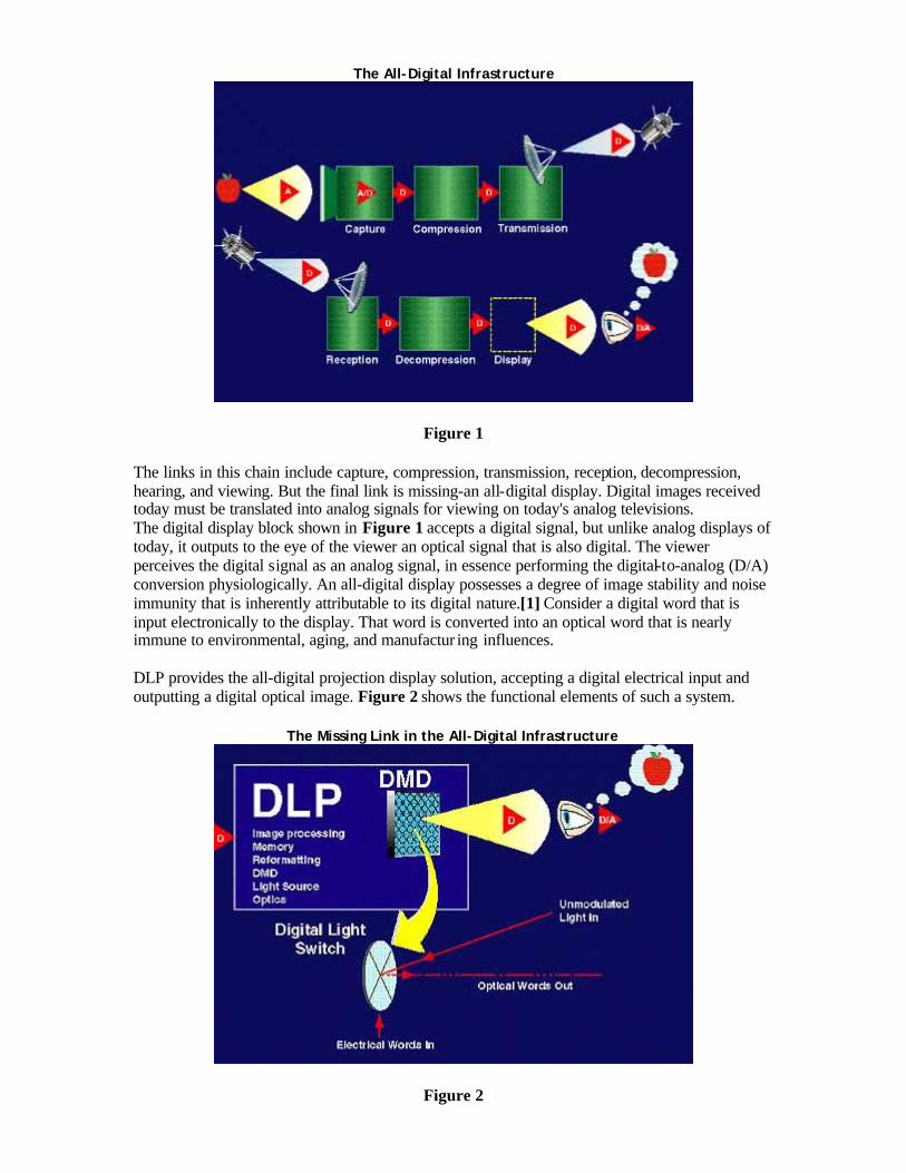
The All-Digital Infrastructure
Figure 1
The links in this chain include capture, compression, transmission, reception, decompression, hearing, and viewing. But the final link is missing-an all-digital display. Digital images received today must be translated into analog signals for viewing on today's analog televisions. The digital display block shown in Figure 1 accepts a digital signal, but unlike analog displays of today, it outputs to the eye of the viewer an optical signal that is also digital. The viewer perceives the digital signal as an analog signal, in essence performing the digital-to-analog (D/A) conversion physiologically. An all-digital display possesses a degree of image stability and noise immunity that is inherently attributable to its digital nature.[1] Consider a digital word that is input electronically to the display. That word is converted into an optical word that is nearly immune to environmental, aging, and manufactur ing influences. DLP provides the all-digital projection display solution, accepting a digital electrical input and outputting a digital optical image. Figure 2 shows the functional elements of such a system.
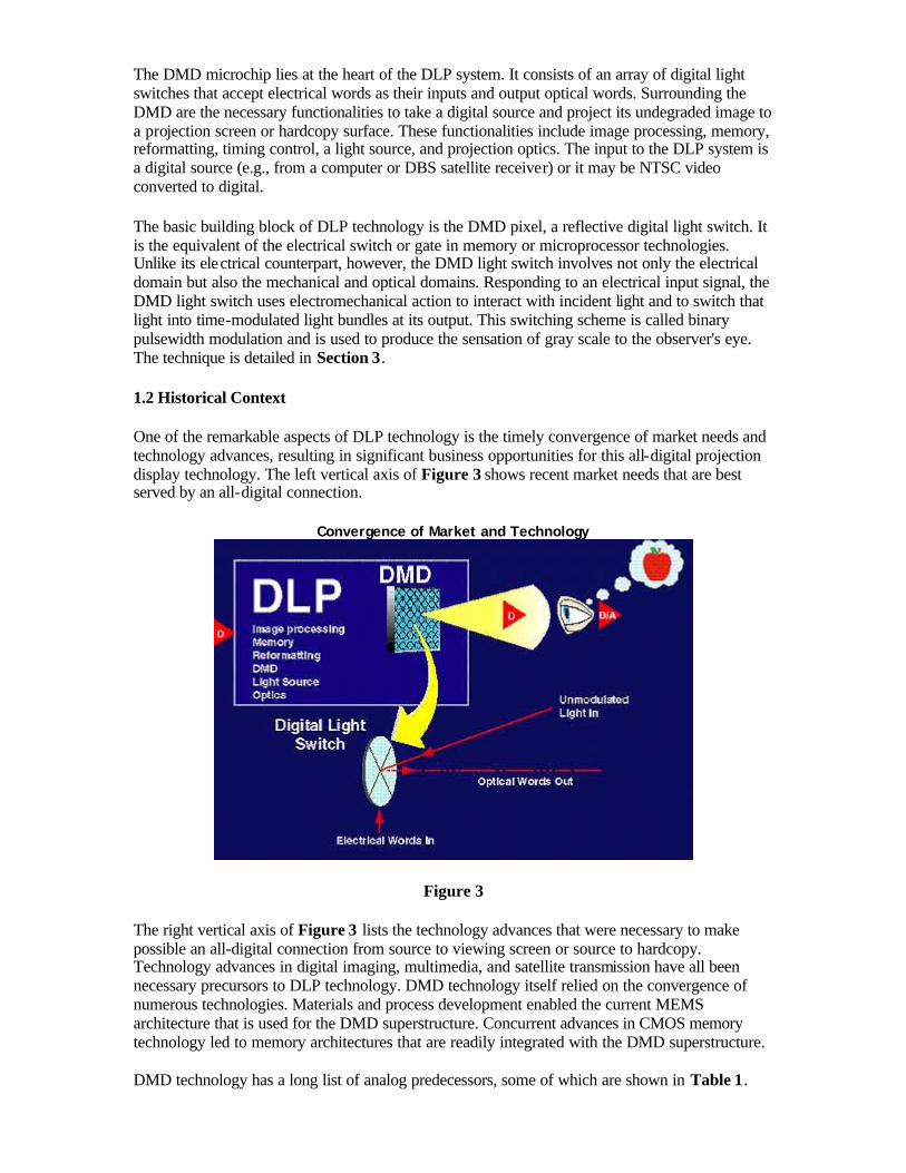
The Missing Link in the All-Digital Infrastructure
Figure 2
The DMD microchip lies at the heart of the DLP system. It consists of an array of digital light switches that accept electrical words as their inputs and output optical words. Surrounding the DMD are the necessary functionalities to take a digital source and project its undegraded image to a projection screen or hardcopy surface. These functionalities include image processing, memory, reformatting, timing control, a light source, and projection optics. The input to the DLP system is a digital source (e.g., from a computer or DBS satellite receiver) or it may be NTSC video converted to digital.
The basic building block of DLP technology is the DMD pixel, a reflective digital light switch. It is the equivalent of the electrical switch or gate in memory or microprocessor technologies. Unlike its electrical counterpart, however, the DMD light switch involves not only the electrical domain but also the mechanical and optical domains. Responding to an electrical input signal, the DMD light switch uses electromechanical action to interact with incident light and to switch that light into time-modulated light bundles at its output. This switching scheme is called binary pulsewidth modulation and is used to produce the sensation of gray scale to the observer's eye. The technique is detailed in Section 3.
1.2 Historical Context
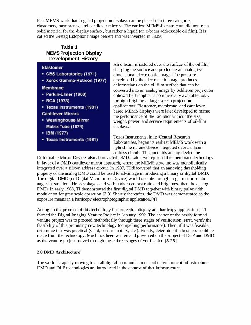
One of the remarkable aspects of DLP technology is the timely convergence of market needs and technology advances, resulting in significant business opportunities for this all-digital projection display technology. The left vertical axis of Figure 3 shows recent market needs that are best served by an all-digital connection.
Convergence of Market and Technology
Figure 3
The right vertical axis of Figure 3 lists the technology advances that were necessary to make possible an all-digital connection from source to viewing screen or source to hardcopy. Technology advances in digital imaging, multimedia, and satellite transmission have all been necessary precursors to DLP technology. DMD technology itself relied on the convergence of numerous technologies. Materials and process development enabled the current MEMS architecture that is used for the DMD superstructure. Concurrent advances in CMOS memory technology led to memory architectures that are readily integrated with the DMD superstructure. DMD technology has a long list of analog predecessors, some of which are shown in Table 1.
Past MEMS work that targeted projection displays can be placed into three categories: elastomers, membranes, and cantilever mirrors. The earliest MEMS-like structure did not use a solid material for the display surface, but rather a liquid (an e-beam addressable oil film). It is called the Gretag Eidophor (image bearer) and was invented in 1939!
Table 1 MEMS Projection Display Development History
An e-beam is rastered over the surface of the oil film, charging the surface and producing an analog two-dimensional electrostatic image. The pressure developed by the electrostatic image produces deformations on the oil film surface that can be converted into an analog image by Schlieren projection optics. The Eidophor is commercially available today for high-brightness, large-screen projection applications. Elastomer, membrane, and cantilever-based MEMS displays were later developed to mimic the performance of the Eidiphor without the size, weight, power, and service requirements of oil-film displays. Texas Instruments, in its Central Research Laboratories, began its earliest MEMS work with a hybrid membrane device integrated over a silicon address circuit. TI named this analog device the
Deformable Mirror Device, also abbreviated DMD. Later, we replaced this membrane technology in favor of a DMD cantilever mirror approach, where the MEMS structure was monolithically integrated over a silicon address circuit. In 1987, TI discovered that an annoying thresholding property of the analog DMD could be used to advantage in producing a binary or digital DMD. The digital DMD (or Digital Micromirror Device) would operate through larger mirror rotation angles at smaller address voltages and with higher contrast ratio and brightness than the analog DMD. In early 1988, TI demonstrated the first digital DMD together with binary pulsewidth modulation for gray scale operation.[2,3] Shortly thereafter, the DMD was demonstrated as the exposure means in a hardcopy electrophotographic application.[4] Acting on the promise of this technology for projection display and hardcopy applications, TI formed the Digital Imaging Venture Project in January 1992. The charter of the newly formed venture project was to proceed methodically through three stages of verification. First, verify the feasibility of this promising new technology (compelling performance). Then, if it was feasible, determine if it was practical (yield, cost, reliability, etc.). Finally, determine if a business could be made from the technology. Much has been written and presented on the subject of DLP and DMD as the venture project moved through these three stages of verification.[5-25]
2.0 DMD Architecture
The world is rapid ly moving to an all-digital communications and entertainment infrastructure. DMD and DLP technologies are introduced in the context of that infrastructure.
2.1 The Mirror as a Switch
The address circuit and electromechanical superstructure of each pixel support one simple function, the fast and precise rotation of an aluminum micromirror, 16 µm square, through angles of +10 and p;10 degrees. Figure 4 illustrates the architecture of one pixel, showing the mirror as semitransparent so that the structure underneath can be observed.
DMD Pixel (transparent mirror, rotated)
Figure 4
The schematic diagram of Figure 5 illustrates the optical switching action of the mirror. When the mirror rotates to its on state (+10 degrees), light from a projection source is directed into the pupil of a projection lens and the pixel appears bright on a projection screen. When the mirror rotates to its off sta te (-10 degrees), light is directed out of the pupil of the projection lens and the pixel appears dark. Thus, the optical switching function is simply the rapid directing of light into or out of the pupil of the projection lens.
Figure 5 DMD Optical Switching Principle
2.2 DMD Cell Structure
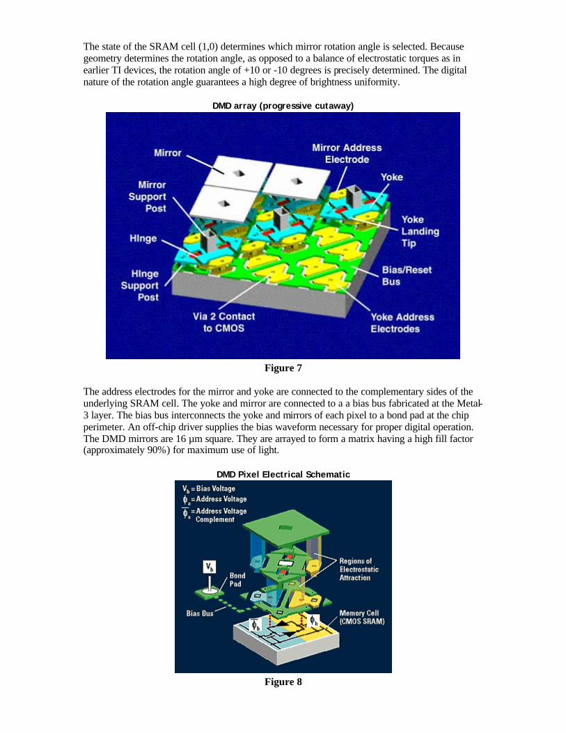
To provide a thorough understanding of the DMD pixel structure and how it is addressed, we employ several figures involving exploded views, cutaway views, and an electrical schematic diagram. Figure 6 shows the pixel structure of Figure 4 in an exploded view illustrating how the various layers interrelate, including the underlying static random access memory (SRAM) cell that is used to address the pixel. Figure 7 shows a progressive cutaway view of a 3 x 3 array of pixels. Figure 8 depicts how each layer is electrically interconnected and defines the bias and address voltages that must be applied to the pixel for proper switching action. The DMD pixel is a monolithically integrated MEMS superstructure cell fabricated over a CMOS SRAM cell. Plasma etching a sacrificial layer develops air gaps between the metal layers of the superstructure. The air gaps free the structure to rotate about two compliant torsion hinges. The mirror is connected to an underlying yoke which in turn is suspended by two thin torsion hinges to support posts. The yoke is electrostatically attracted to the underlying yoke address electrodes. The mirror is electrostatically attracted to mirror address electrodes. The mirror and yoke rotate until the yoke comes to rest against mechanical stops that are at the same potential as the yoke. The position of the mechanical stops limits the mirror rotation angle to +10 or -10 degrees.
DMD Pixel Exploded View Z
Figure 6
The state of the SRAM cell (1,0) determines which mirror rotation angle is selected. Because geometry determines the rotation angle, as opposed to a balance of electrostatic torques as in earlier TI devices, the rotation angle of +10 or -10 degrees is precisely determined. The digital nature of the rotation angle guarantees a high degree of brightness uniformity.
DMD array (progressive cutaway)
Figure 7
The address electrodes for the mirror and yoke are connected to the complementary sides of the underlying SRAM cell. The yoke and mirror are connected to a a bias bus fabricated at the Metal-3 layer. The bias bus interconnects the yoke and mirrors of each pixel to a bond pad at the chip perimeter. An off-chip driver supplies the bias waveform necessary for proper digital operation. The DMD mirrors are 16 µm square. They are arrayed to form a matrix having a high fill factor (approximately 90%) for maximum use of light.
DMD Pixel Electrical Schematic
Figure 8
2.3 Digital Nature of the DMD
The DMD pixel is operated in an electrostatically bistable mode to minimize the address voltage requirements. In this manner, we can achieve large rotation angles with conventional 5 volt CMOS devices. To this end, a bias voltage is applied to the yoke and mirror (see Figure 8). For a mirror that is in its flat or quiescent state, the bias produces no net torque. Nevertheless, the effect of bias on a flat-state mirror is profound.[3] To best illustrate this principle, the energy of a mirror is calculated as a function of rotation angle and bias, as shown in Figure 9. It is assumed that the address voltage is zero. We use energy rather than torques to illustrate the principle, because the stable equilibrium position of the mirror in energy space is simply the position of the local minimum. The stable equilibrium postion of the mirror is determined by the balance of a linear hinge restoring torque and a counteracting nonlinear electrostatic torque. When they are equal, a condition of equilibrium has been achieved and under this condition, the energy is at a local minimum (stable equilibrium) or local maximum (unstable equilibrium).
Potential Energy of a Mirror as a Function of Angle and Bias (address voltage = 0)
Figure 9
For zero bias voltage (upper red curve), the energy of the mirror about zero rotation angle increases parabolically with angle. The parabolic increase results from the energy that must be expended to rotate the hinge. Under the condition of zero bias voltage, the stable equilibrium position is at zero angle; i.e., with only the hinge torques acting on the yoke and mirror, the mirror wants to settle and reside in the flat state. As the bias voltage increases from zero (lower red curve), the potential energy begins to decrease for larger mirror rotation angles because of the attractive torque produced by the bias. The bias does not produce a net torque when the mirror is in its flat state. But the bias does produce a net torque at non-zero rotation angles when the electrostatic symmetry has been broken. When one side of the yoke and hinge is closer to the address electrodes, that side attracts more strongly than the other. At sufficiently high bias voltages, stable equilibrium positions develop at +10 or -10 degrees (yellow curves). The DMD pixel now has three stable equilibrium positions (0, +10 deg, -10 deg). Further increases in bias cause the energy barrier to disappear between the flat state and +10/-10 degrees (green curves). Under this condition, the DMD pixel has only two stable equilibrium postions (+10 or -10 degrees) and is bistable. The bias voltage to just achieve the bistable
condition is called the bistable threshold voltage. It is the bistable bias condition that leads to the smallest address voltage requirement. Just as a ball at the top of a hill requires just a gentle nudge to cause it to roll down the hill in either direction, so do the mirror and yoke require only enough address voltage torque to overcome any imperfections in the structure caused by the hinge or by structural alignment.
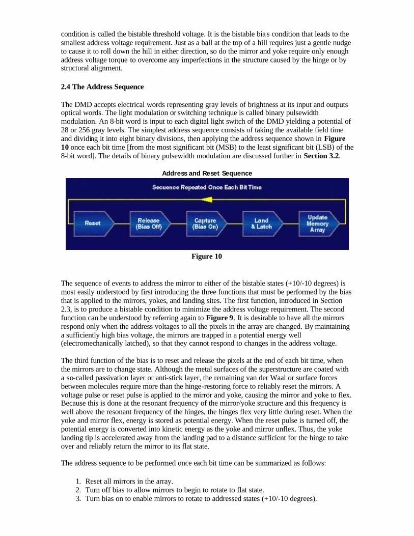
2.4 The Address Sequence
The DMD accepts electrical words representing gray levels of brightness at its input and outputs optical words. The light modulation or switching technique is called binary pulsewidth modulation. An 8-bit word is input to each digital light switch of the DMD yielding a potential of 28 or 256 gray levels. The simplest address sequence consists of taking the available field time and dividing it into eight binary divisions, then applying the address sequence shown in Figure 10 once each bit time [from the most significant bit (MSB) to the least significant bit (LSB) of the 8-bit word]. The details of binary pulsewidth modulation are discussed further in Section 3.2.
Address and Reset Sequence
Figure 10
The sequence of events to address the mirror to either of the bistable states (+10/-10 degrees) is most easily understood by first introducing the three functions that must be performed by the bias that is applied to the mirrors, yokes, and landing sites. The first function, introduced in Section 2.3, is to produce a bistable condition to minimize the address voltage requirement. The second function can be understood by referring again to Figure 9. It is desirable to have all the mirrors respond only when the address voltages to all the pixels in the array are changed. By maintaining a sufficiently high bias voltage, the mirrors are trapped in a potential energy well (electromechanically latched), so that they cannot respond to changes in the address voltage. The third function of the bias is to reset and release the pixels at the end of each bit time, when the mirrors are to change state. Although the metal surfaces of the superstructure are coated with a so-called passivation layer or anti-stick layer, the remaining van der Waal or surface forces between molecules require more than the hinge-restoring force to reliably reset the mirrors. A voltage pulse or reset pulse is applied to the mirror and yoke, causing the mirror and yoke to flex. Because this is done at the resonant frequency of the mirror/yoke structure and this frequency is well above the resonant frequency of the hinges, the hinges flex very little during reset. When the yoke and mirror flex, energy is stored as potential energy. When the reset pulse is turned off, the potential energy is converted into kinetic energy as the yoke and mirror unflex. Thus, the yoke landing tip is accelerated away from the landing pad to a distance sufficient for the hinge to take over and reliably return the mirror to its flat state. The address sequence to be performed once each bit time can be summarized as follows:
1. Reset all mirrors in the array. 2. Turn off bias to allow mirrors to begin to rotate to flat state. 3. Turn bias on to enable mirrors to rotate to addressed states (+10/-10 degrees).
4. Keep bias on to latch mirrors (they will not respond to new address states). 5. Address SRAM array under the mirrors, one line at a time. 6. Repeat sequence beginning at step 1.
2.5 Evolution of the DMD Architecture
The cell structure shown in Figures 6 and 7 is the latest in a series of architectural changes that have improved the optical performance and reliability of the DMD digital light switch (see Figure 11). The basic bistable concept was developed in the Central Research Laboratories of Texas Instruments (now Corporate Research & Development). The first structure, known as the conventional pixel, did not hide the mechanical structures of the hinges or the support posts. This resulted in less area available for the mirror and greater light diffraction from the exposed mechanical structures. The result was a contrast ratio and optical efficiency that could not support a commercial business.
Evolution of DMD Pixel
Figure 11
The first improvement made by the newly formed Digital Imaging Venture Project of Texas Instruments was to hide the hinges and support posts under the mirror (Hidden Hinge 1). This modification resulted in a greater mirror area and less light diffraction with an attendant improvement in contrast ratio (>100:1) and greater optical efficiency. But this structure could not work reliably with 5 volt CMOS levels. Two more superstructure designs were required before reliable operation was achieved. The current structure (Hidden Hinge 3) maximizes the available area for electrostatic attraction, using both the yoke and mirror as active elements. Thus, almost every bit of area is used to develop electrostatic torque, resulting in greater electrical efficiency and reliability.
3.0 Projection Operation
3.1 DMD Optical Switching Principle
The optical switching principle is briefly discussed in Section 2.1 and illustrated in Figure 5 . Light from a projection source illuminates the DMD array at an angle of +2qL from the normal to the plane of mirrors in their flat state. The angle qL is the rotation angle of the mirror when the yoke is touching its mechanical stops, or landed. The mirror in its flat state reflects the incident light to an angle of -2qL. The projection lens is designed so that flat state light misses the pupil of
the projection lens, allowing very little light to be projected through the lens. But the mirrors are only briefly at the flat state as they make a transition from one landed state to the other. When the mirror is in its off state, the reflected light is further removed from the pupil of the projection lens and even less light is collected by the projection lens. When the mirror is in its on state, the reflected light is directed into the pupil of the projection lens, and nearly all the light is collected by the projection lens and imaged to the projection screen. Because of the large rotation angles of the mirror, the off-state light and on-state light are widely separated, allowing fast projection optics to be used. The result is efficient light collection while maintaining a high contrast ratio.
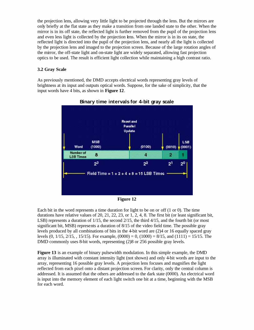
3.2 Gray Scale
As previously mentioned, the DMD accepts electrical words representing gray levels of brightness at its input and outputs optical words. Suppose, for the sake of simplicity, that the input words have 4 bits, as shown in Figure 12.
Binary time intervals for 4-bit gray scale
Figure 12
Each bit in the word represents a time duration for light to be on or off (1 or 0). The time durations have relative values of 20, 21, 22, 23, or 1, 2, 4, 8. The first bit (or least significant bit, LSB) represents a duration of 1/15, the second 2/15, the third 4/15, and the fourth bit (or most significant bit, MSB) represents a duration of 8/15 of the video field time. The possible gray levels produced by all combinations of bits in the 4-bit word are (2)4 or 16 equally spaced gray levels (0, 1/15, 2/15, , 15/15). For example, (0000) = 0, (1000) = 8/15, and (1111) = 15/15. The DMD commonly uses 8-bit words, representing (2)8 or 256 possible gray levels.
Figure 13 is an example of binary pulsewidth modulation. In this simple example, the DMD array is illuminated with constant intensity light (not shown) and only 4-bit words are input to the array, representing 16 possible gray levels. A projection lens focuses and magnifies the light reflected from each pixel onto a distant projection screen. For clarity, only the central column is addressed. It is assumed that the others are addressed to the dark state (0000). An electrical word is input into the memory element of each light switch one bit at a time, beginning with the MSB for each word.
Example of DMD Array of Digital Light Switches Projecting Gray Levels
Figure 13
When the entire array of light switches has been addressed with the MSB, the individual pixels are enabled (reset) so that they can respond in parallel to their MSB state (1 or 0). During each bit time, the next bit is loaded into the memory array. At the end of each bit time, the pixels are reset and they respond in parallel to the next address bit. The process is repeated until all address bits are loaded into memory. Incident light is reflected from the light switches and is switched or modulated into light bundles having durations represented by each bit in the electrical word. To an observer, the light bundles occur over such a small time compared to the integration time of the eye that they give the physical sensation of light having a constant intensity represented by the value of the 4-bit input word.
3.3 Optical Switching Time
Conventionally, the DMD is addressed with an 8-bit word yielding (2)8 = 256 gray levels. For 8-bit gray scale, the minimum duration of a light bundle has to be 1/256 of the total field time. For a one-chip projection system, the DMD is sequentially illuminated with the three primary colors, red, green, and blue (RGB). For NTSC video, the time occupied by one color field is 163 ms or 5.3 ms. The LSB time is, therefore, (16/3) x (1256) = 0.021 ms or 21 µs. The optical switching time of the DMD and projection lens combination must be small compared to 21 µs in order to support 8-bit gray scale for a single -chip projector.
Mechanical and Optical Switching Response Figure 14
Figure 14 shows the measured switching response of the DMD. Three variables are plotted as a function of time: the bias/reset voltage, the cross-over transition from +10 degrees to -10 degrees, and the same-side transition for a mirror that is to remain at +10 degrees. Shortly before the reset pulse is applied, all the SRAM memory cells in the DMD array are updated. The mirrors have not
responded to the new memory states because the bias voltage keeps them electromechanically latched.
The mechanical switching time is the interval between when the reset pulse is applied and the crossover mirrors have landed and settled to a level where they are electromechancially latched and the SRAM cells can once again be updated. The optical switching time is the time from when the light first enters the aperture of the projection lens to when the aperture is fully filled with light from the rotating mirror. Figure 14 shows that the mechanical switching time is measured as ~15 µs and the optical switching time is ~2 µs. The optical switching time is ~10% of the LSB time, and therefore supports 8-bit gray scale under the most demanding condition of a single -chip projector.
3.4 Projection Systems
The choice of how many DMD chips (one, two, or three) to employ in a DLP projection system is determined by the tradeoff between cost, light efficiency, power dissipation, weight, and volume. The single-chip projection system uses a color wheel containing the three primary colors, RGB. The DMD chip is alternately illuminated with RGB. The two-chip system uses dichroic mirrors to split the red (R) from the green and blue (GB). The R illuminates one chip exclusively and a color wheel containing GB alternately illuminates the second chip. The choice of which color goes exclusively to one chip is determined by the spectral content of the lamp. Metal-halide lamps have a high color temperature that produces higher intensities for GB compared to R. Therefore, for that type of lamp, the red is directed exclusively to one chip. This makes up for the deficiency in R and provides the correct color balance for the projected images. Finally, the three-chip system has dichroic mirrors that split RGB separately so that each chip is continuously illuminated with one color. Figure 15 is an example of a single-chip DLP projection system. The light source is usually metal halide because of its greater luminous efficiency (lumens delivered per electrical watt dissipated). A condenser lens collects the light, which is imaged onto the surface of a transmissive color wheel. A second lens collects the light that passes through the color wheel and evenly illuminates the surface of the DMD. Depending on the rotational state of the mirror (+10 or -10 degrees), the light is directed either into the pupil of the projection lens (on) or away from the pupil of the projection lens (off). The projection lens has two functions: (1) to collect the light from each on-state mirror, and (2) to project an enlarged image of the mirror surface to a projection screen.
Single-chip DLP projection system
Figure 15
Figure 16 shows a front-projection display image. The field of view of the projection lens has been increased to show the chip perimeter, including the bond pads and wires. Normally, the chip perimeter has a light shield over it so that the display area is surrounded by a black background.
DLP Front-projection Display Showing Entire Chip Area
Figure 16
4.0 Fabrication
The DMD superstructure is monolithically fabricated over an SRAM address circuit by conventional semiconductor processing techniques, including the steps of sputter metal deposition, lithography, and plasma etching. Plasma etching of an organic sacrificial layer forms the air gap. This sacrificial layer is simply a conventional, hardened positive photoresist layer. However, several of the packaging and testing steps in the fabrication flow differ significantly
from those in a conventional CMOS wafer flow. These differences arise because of the mechanical and optical nature of the product.
4.1 Wafer Process Flow
Figure 17 outlines the DMD superstructure fabrication and packaging flow. A more detailed account of the wafer fabrication portion of the flow is shown in Figure 18. The superstructure process begins with a completed SRAM address circuit employing 0.8 µm, double -level metal CMOS technology. A thick oxide is deposited over Metal-2 of the CMOS and then planarized using a chemical mechanical polish (CMP) technique. The CMP step provides a completely flat substrate for DMD superstructure fabrication, ensuring that the projector's brightness uniformity and contrast ratio are not degraded.
DMD Process Flow
Figure 17
The superstructure process begins with deposition and patterning of aluminum for the Metal-3 layer. An organic sacrificial layer (Spacer-1) is then spin-coated, lithographically patterned, and hardened. The holes or spacervias that are patterned in the spacer form metal support posts after the yoke metal covers their sidewalls. These support posts support the hinges and the electrically independent mirror address electrodes.
Details of DMD Superstructure Process
Figure 18
Next, a thin metal layer (typically 600 Angstroms) is sputter-deposited for the hinges. This metal layer is not patterned at this step, but rather is covered with a plasma-deposited layer of SiO2. This oxide layer is patterned in the shape of the hinges and used as an etch mask for the hinges later in the process. A thicker layer of aluminum is sputter-deposited for the yoke layer, covering the hinge metal and the hinge oxide masks. A second layer of plasma SiO2 is then deposited over the yoke metal to act as a mask. This layer is patterned in the shape of the yoke structures, with an opening over the hinges. A plasma etch patterns both the yoke and hinge metallization layers. As the yoke metal is etched away from over the hinges, the plasma etch stops on the hinge oxide mask. The plasma continues etching into the hinge layer to define the hinge geometries. In this manner, a single plasma etch defines both the thin hinges and the much thicker yoke structures. A significant advantage to this one-step etch process is the architectural benefit of having the hinge metal continuous everywhere under the yoke metallization layer. A second organic sacrificial layer (Spacer-2) is spin-coated, lithographically patterned, and hardened. The holes or spacervias that are patterned in this spacer form the support posts that secure the mirrors to the underlying yokes. Finally, an aluminum layer is sputter-deposited over Spacer-2 to form the mirrors. It also is patterned with an oxide etch mask in the same manner as the yoke layer. This completes the superstructure process with the exception of removing the sacrificial layers to form the air gaps.
4.2 Packaging Flow and Test
After the air gaps are formed, the DMD superstructure is too delicate to survive the conventional saw and cleaning process that is necessary to separate the chips from one another. Therefore, the wafers are partially sawed along the chip scribe lines to a depth that will allow them to be easily broken after the air gaps are formed. The partially sawed and cleaned wafers then proceed to a plasma etcher that is used to selectively strip the organic sacrificial layers from under the DMD
mirror, yoke, and hinge layers. Following this process is a so-called passivation step wherein a thin, self-limiting, anti-stick layer is deposited to lower the surface energy of the contacting parts of the DMD superstructure. This passivation step, in conjunction with the electronic reset sequence, ensures reliable operation for the life of the device. Before separating the chips from one another, each chip is tested (To) for full electrical and optical functionality by an automated wafer tester. The wafers are then mounted onto an adhesive backing so that they will maintain their orientation with respect to one another after chip separation. Each wafer proceeds into a machine that uses a dome-shaped flange to controllably break the wafer along its scribe lines to separate the chips. The separated chips that have passed testing are then selected by a pick-and-place machine and accurately placed into a package and attached with an adhesive. After bond wire attachment, the chips in their individual packages are plasma-cleaned (plasma activation) and passivated again to ensure a high-quality anti-stick layer. Immediately following this operation, a lid with a high-quality optical window is welded to the package weld ring to ensure a hermetic and clean environment for the DMD. Another test (T2) is performed on each packaged part to ensure full functionality. This test is followed by an elevated temperature, full electromechanical operation burn-in and then another test (T3). Another burn-in and several more tests are necessary before the finished DMD parts are qualified.
SEM photomicrographs of completed DMD chips after spacer removal
Figure 19
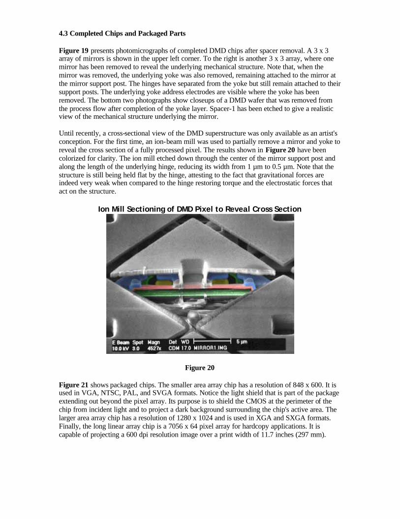
4.3 Completed Chips and Packaged Parts
Figure 19 presents photomicrographs of completed DMD chips after spacer removal. A 3 x 3 array of mirrors is shown in the upper left corner. To the right is another 3 x 3 array, where one mirror has been removed to reveal the underlying mechanical structure. Note that, when the mirror was removed, the underlying yoke was also removed, remaining attached to the mirror at the mirror support post. The hinges have separated from the yoke but still remain attached to their support posts. The underlying yoke address electrodes are visible where the yoke has been removed. The bottom two photographs show closeups of a DMD wafer that was removed from the process flow after completion of the yoke layer. Spacer-1 has been etched to give a realistic view of the mechanical structure underlying the mirror. Until recently, a cross-sectional view of the DMD superstructure was only available as an artist's conception. For the first time, an ion-beam mill was used to partially remove a mirror and yoke to reveal the cross section of a fully processed pixel. The results shown in Figure 20 have been colorized for clarity. The ion mill etched down through the center of the mirror support post and along the length of the underlying hinge, reducing its width from 1 µm to 0.5 µm. Note that the structure is still being held flat by the hinge, attesting to the fact that gravitational forces are indeed very weak when compared to the hinge restoring torque and the electrostatic forces that act on the structure.
Ion Mill Sectioning of DMD Pixel to Reveal Cross Section
Figure 20
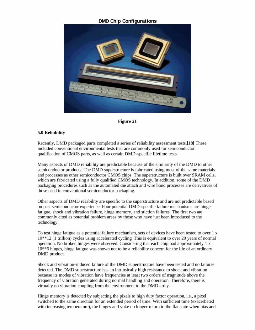
Figure 21 shows packaged chips. The smaller area array chip has a resolution of 848 x 600. It is used in VGA, NTSC, PAL, and SVGA formats. Notice the light shield that is part of the package extending out beyond the pixel array. Its purpose is to shield the CMOS at the perimeter of the chip from incident light and to project a dark background surrounding the chip's active area. The larger area array chip has a resolution of 1280 x 1024 and is used in XGA and SXGA formats. Finally, the long linear array chip is a 7056 x 64 pixel array for hardcopy applications. It is capable of projecting a 600 dpi resolution image over a print width of 11.7 inches (297 mm).
DMD Chip Configurations
Figure 21
5.0 Reliability
Recently, DMD packaged parts completed a series of reliability assessment tests.[18] These included conventional environmental tests that are commonly used for semiconductor qualification of CMOS parts, as well as certain DMD-specific lifetime tests. Many aspects of DMD reliability are predictable because of the similarity of the DMD to other semiconductor products. The DMD superstructure is fabricated using most of the same materials and processes as other semiconductor CMOS chips. The superstructure is built over SRAM cells, which are fabricated using a fully qualified CMOS technology. In addition, some of the DMD packaging procedures such as the automated die attach and wire bond processes are derivatives of those used in conventional semiconductor packaging. Other aspects of DMD reliability are specific to the superstructure and are not predictable based on past semiconductor experience. Four potential DMD-specific failure mechanisms are hinge fatigue, shock and vibration failure, hinge memory, and stiction failures. The first two are commonly cited as potential problem areas by those who have just been introduced to the technology. To test hinge fatigue as a potential failure mechanism, sets of devices have been tested to over 1 x 10**12 (1 trillion) cycles using accelerated cycling. This is equivalent to over 20 years of normal operation. No broken hinges were observed. Considering that each chip had approximately 1 x 10**6 hinges, hinge fatigue was shown not to be a reliability concern for the life of an ordinary DMD product. Shock and vibration-induced failure of the DMD superstructure have been tested and no failures detected. The DMD superstructure has an intrinsically high resistance to shock and vibration because its modes of vibration have frequencies at least two orders of magnitude above the frequency of vibration generated during normal handling and operation. Therefore, there is virtually no vibration coupling from the environment to the DMD array. Hinge memory is detected by subjecting the pixels to high duty factor operation, i.e., a pixel switched to the same direction for an extended period of time. With sufficient time (exacerbated with increasing temperature), the hinges and yoke no longer return to the flat state when bias and
address voltages are removed. If the rotation angle of the yoke is excessive, the pixel will lose address margin and no longer switch to both states. Metal creep is responsible for hinge memory. A study of alternative hinge materials yielded an alloy that has a low creep rate and preserves the address margin over the operating life of the DMD. Stiction failures are caused by an excessive adhesive force between the landing tip and its landing site. If the stiction level is sufficiently high, the electronic reset sequence will not overcome the stiction force and the pixel will fail to switch. Adhesive forces are produced by capillary condensation of volatiles such as water and by short-range forces between surface molecules called van der Waals forces. As mentioned in Section 4.1, to reduce stiction levels, a thin, self-limiting, anti-stick layer is deposited to lower the surface energy of the contacting parts. This so-called passivation step is followed by hermetic packaging to keep water vapor levels low and to prevent capillary condensation. Together, these processes ensure reliable reset operation for the life of the DMD.
6.0 DLP Business Opportunities
We stated earlier that one of the remarkable aspects of DLP technology is the timely convergence of market needs and technology advances resulting in significant business opportunities for this all-digital projection display technology. The market needs for DLP technology fall into two general categories: displays and hardcopy.
6.1 Hardcopy in Evaluation
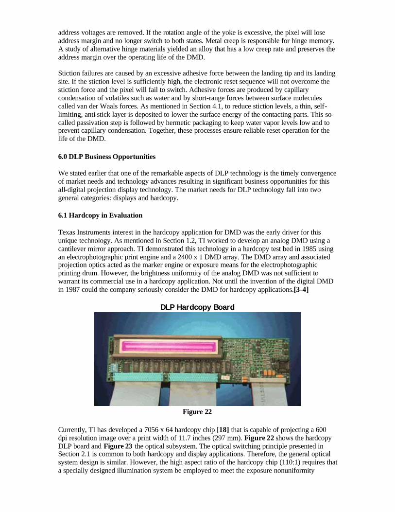
Texas Instruments interest in the hardcopy application for DMD was the early driver for this unique technology. As mentioned in Section 1.2, TI worked to develop an analog DMD using a cantilever mirror approach. TI demonstrated this technology in a hardcopy test bed in 1985 using an electrophotographic print engine and a 2400 x 1 DMD array. The DMD array and associated projection optics acted as the marker engine or exposure means for the electrophotographic printing drum. However, the brightness uniformity of the analog DMD was not sufficient to warrant its commercial use in a hardcopy application. Not until the invention of the digital DMD in 1987 could the company seriously consider the DMD for hardcopy applications.[3-4]
DLP Hardcopy Board
Figure 22
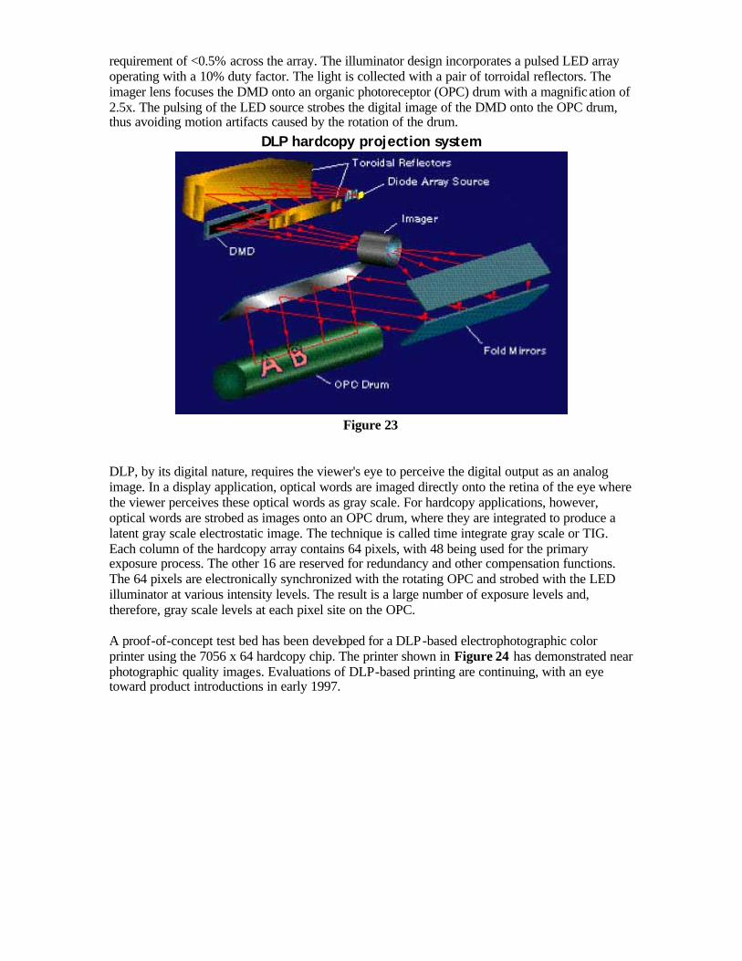
Currently, TI has developed a 7056 x 64 hardcopy chip [18] that is capable of projecting a 600 dpi resolution image over a print width of 11.7 inches (297 mm). Figure 22 shows the hardcopy DLP board and Figure 23 the optical subsystem. The optical switching principle presented in Section 2.1 is common to both hardcopy and display applications. Therefore, the general optical system design is similar. However, the high aspect ratio of the hardcopy chip (110:1) requires that a specially designed illumination system be employed to meet the exposure nonuniformity
requirement of <0.5% across the array. The illuminator design incorporates a pulsed LED array operating with a 10% duty factor. The light is collected with a pair of torroidal reflectors. The imager lens focuses the DMD onto an organic photoreceptor (OPC) drum with a magnification of 2.5x. The pulsing of the LED source strobes the digital image of the DMD onto the OPC drum, thus avoiding motion artifacts caused by the rotation of the drum.
DLP hardcopy projection system
Figure 23
DLP, by its digital nature, requires the viewer's eye to perceive the digital output as an analog image. In a display application, optical words are imaged directly onto the retina of the eye where the viewer perceives these optical words as gray scale. For hardcopy applications, however, optical words are strobed as images onto an OPC drum, where they are integrated to produce a latent gray scale electrostatic image. The technique is called time integrate gray scale or TIG. Each column of the hardcopy array contains 64 pixels, with 48 being used for the primary exposure process. The other 16 are reserved for redundancy and other compensation functions. The 64 pixels are electronically synchronized with the rotating OPC and strobed with the LED illuminator at various intensity levels. The result is a large number of exposure levels and, therefore, gray scale levels at each pixel site on the OPC. A proof-of-concept test bed has been developed for a DLP-based electrophotographic color printer using the 7056 x 64 hardcopy chip. The printer shown in Figure 24 has demonstrated near photographic quality images. Evaluations of DLP-based printing are continuing, with an eye toward product introductions in early 1997.
DLP-Based Printer Prototype and Print Samples
Figure 24
6.2 Display opportunities and products
The market opportunities for DLP projection displays can be divided into three market segments: professional, business and consumer. [25] Table 2 describes the group settings that are served by each display segment.
Table 2 Display Opportunities
Some general statements can be made about each market segment. The professional segment requires front projection and the largest screen size. Several thousand lumens must be delivered to the screen to meet brightness level requirements. To achieve this performance level requires a three-chip DLP system for maximum luminous efficiency (lumens delivered per electrical watt dissipated by the projection lamp). The business segment requires front projection and portability, implying low weight and small volume. A single -chip DLP system and a very efficient metal halide projection lamp are essential to reducing the weight and volume while maintaining brightness. Finally, in the consumer segment, brightness and reliability are keys to capturing the market, but at an affordable price. A brightness/cost tradeoff may indicate that the optimum solution for this market segment is a two-chip DLP system. Consumer projectors may be front or rear projection. Texas Instruments has developed a strategy for the
projection display business. TI will not enter the market directly but rather seek partners who are market makers in the various segments of the projection display business. Texas Instruments will build on its semiconductor product portfolio to deliver DLP subsystems to its partners. These
subsystems will include the DMD as well as digital signal processing (DSP), memory, and other functionalities, thus providing a complete DLP solution for each business partner. Each partner will begin with the DLP subsystem and will complete the manufacture of the display, differentiating it according to the needs of the market the partner serves.
Single-chip DLP board for business projector
Figure 25
The first DLP product will be a VGA resolution (640 x 480) single -chip digital display engine to be shipped in 4th quarter 1995 (4Q95). It is designed to serve the business display market where portability is key. A digital display engine, or DDE, is the DLP subsystem ready for integration with a video interface, power supply, sound, controls, and a cabinet. Figure 25 shows the DLP board for the DDE and Figure 26 shows the complete DDE. The DDE will deliver over 300 lumens to the screen and will weigh approximately 10 pounds. Figures 27 and 28 are examples of prototype DLP projection displays.
Single-Chip Digital Display Engine (DDE) for Business Projector
Figure 26
The DLP video products roadmap begins with the introduction of a business projector at VGA resolutions in 4Q95, followed by SVGA and XGA resolution products in 1996. Professional products will begin in 1996 starting at SVGA and NTSC/PAL resolutions. In early 1997, DLP products will enter the consumer market. Ease of configurability of DLP video products is key to their success in the diverse markets in which they must compete.
7.0 Summary
The convergence of market needs and technology advances has created a unique business opportunity for an all-digital display technology based on the Digital Micromirror Device (DMD). This paper presents an overview of this important new technology in terms of its architecture, projection operation, fabrication, and reliability. Digital Light Processing (DLP) systems incorporating the DMD are being developed for projection displays and hardcopy applications. Hardcopy systems using DLP are in an evaluation phase, with promising, near photographic quality printing having already been demonstrated. DLP-based projection display systems have been demonstrated in a variety of sizes and form factors. By the end of 1995, the first projection displays based on DLP will be available on the market.
8.0 Acknowledgements
The author wishes to express his gratitude to the members of the Digital Imaging Venture Project who, through their inspiration, dedication, and perseverance have transformed DLP technology from a laboratory experiment into an important new business opportunity.
9.0 References
1. R.J. Gove, "DMD Display Systems: The Impact of an All-Digital Display," Society for Information Display International Symposium (June 1994).
2. L.J. Hornbeck and W.E. Nelson, "Bistable Deformable Mirror Device," OSA Technical Digest Series Vol. 8, Spatial Light Modulators and Applications, p. 107 (1988).
3. L.J. Hornbeck, "Deformable-Mirror Spatial Light Modulators," Spatial Light Modulators and Applications III, SPIE Critical Reviews, Vol. 1150, pp. 86-102 (August 1989).
4. W.E. Nelson, L.J. Hornbeck, Micromechanical Spatial Light Modulator for Electrophotographic Printers, SPSE Fourth International Congress on Advances in Non-Impact Printing Technologies, p. 427, March 20, 1988.
5. J.B. Sampsell, "An Overview of Texas Instruments Digital Micromirror Device (DMD) and Its Application to Projection Displays," Society for Information Display Internatl. Symposium Digest of Tech. Papers, Vol. 24, pp. 1012-1015 (May 1993).
6. L.J. Hornbeck, "Current Status of the Digital Micromirror Device (DMD) for Projection Television Applications (Invited Paper)," International Electron Devices Technical Digest, pp. 381-384 (1993).
7. J.M Younse and D.W. Monk, "The Digital Micromirror Device (DMD) and Its Transition to HDTV," Proc. of 13th International Display Research Conf. (Late News Papers), pp. 613-616 (August 31-September 3, 1993).
8. J.B. Sampsell, "The Digital Micromirror Device," 7th ICSS&A, Yokohama, Japan (1993). 9. J.M. Younse, "Mirrors on a Chip," IEEE Spectrum, pp. 27-31 (November 1993). 10. M.A. Mignardi, "Digital Micromirror Array for Projection TV," Solid State Technology,
Vol. 37, pp. 63-66 (July 1994). 11. V. Markandey et al., "Motion Adaptive Deinterlacer for DMD (Digital Micromirror
Device) Based Digital Television," IEEE Trans. on Consumer Electronics, Vol. 40, No. 3, pp. 735-742 (August 1994).
12. V. Markandey and R. Gove, "Digital Display Systems Based on the Digital Micromirror Device," SMPTE 136th Technical Conference and World Media Expo (October 1994).
13. D.W. Monk, "Digital Micromirror Device Technology for Projection Displays," EID Exhibition & Conference, Sandown, UK (October 26, 1994).
14. R.J. Gove et al., "High Definition Display System Based on Digital Micromirror Device," International Workshop on HDTV (October 1994).
15. J.B. Sampsell, "An Overview of the Performance Envelope of Digital Micromirror Device Based Projection Display Systems," SID 94 Digest, pp. 669-672 (1994).
16. C. Tew et al., "Electronic Control of a Digital Micromirror Device for Projection Displays," IEEE International Solid -State Circuits Digest of Technical Papers, Vol. 37, pp. 130-131 (1994).
17. W.E. Nelson and R.L. Bhuva, "Digital Micromirror Device Imaging Bar for Hardcopy," Color Hardcopy and Graphic Arts IV, SPIE, Vol. 2413, San Jose, CA (February 1995).
18. M.R. Douglass and D.M. Kozuch, "DMD Reliability Assessment for Large-Area Displays," Society for Information Display International Symposium Digest of Technical Papers, Vol. 26 (Applications Session A3), pp. 49-52 (May 23-25, 1995).
19. E. Chiu et al., "Design and Implementation of a 525 mm2 CMOS Digital Micromirror Device (DMD) Chip," IEEE VLSI Conference (May 1995).
20. B.R. Critchley, P.W. Blaxtan, B. Eckersley, R.O. Gale, and M. Burton, "Picture Quality in Large Screen Projectors Using the Digital Micromirror Device," SID 95 Digest, pp. 524-527 (1995).
21. G. Sextro, T. Ballew, J. Iwal, "High-Definition Projection System Using DMD Display Technology," SID 95 Digest, pp. 70-73 (1995).
22. G. Feather, "Digital Light Processing: Projection Display Advantages of the Digital Micromirror Device," 19th Montreux Television Symposium (June 1995).
23. G. Hewlett and W. Werner, "Analysis of Electronic Cinema Projection with the Texas Instruments Digital Micromirror Device Display System," presented at 137th SMPTE Technical Conference (September 6-9, 1995).
24. L. Yoder, "The Fundamentals of Using the Digita l Micromirror Device (DMD) for Projection Displays," presented at International Conference on Integrated Micro/Nanotechnology for Space Applications, Houston, Texas (October 1995).
25. J.M. Younse, "Projection Display Systems Based on the Digital Micromirror Device (DMD)," SPIE Conference on Microelectronic Structures and Micrelectromechanical Devices for Optical Processing and Multimedia Applications, Austin, Texas (October 24, 1995).