DIGITAL NOTES ON COMPUTER ORGANIZATION B.TECH II YEAR - I SEM (2018-19) DEPARTMENT OF INFORMATION TECHNOLOGY MALLA REDDY COLLEGE OF ENGINEERING & TECHNOLOGY (Autonomous Institution – UGC, Govt. of India) (Affiliated to JNTUH, Hyderabad, Approved by AICTE - Accredited by NBA & NAAC – ‘A’ Grade - ISO 9001:2015 Certified) Maisammaguda, Dhulapally (Post Via. Hakimpet), Secunderabad – 500100, Telangana State, INDIA.
Transcript
DIGITAL NOTES
ON COMPUTER ORGANIZATION
B.TECH II YEAR - I SEM (2018-19)
DEPARTMENT OF INFORMATION TECHNOLOGY
MALLA REDDY COLLEGE OF ENGINEERING & TECHNOLOGY (Autonomous Institution – UGC, Govt. of India)
(Affiliated to JNTUH, Hyderabad, Approved by AICTE - Accredited by NBA & NAAC – ‘A’ Grade - ISO 9001:2015 Certified) Maisammaguda, Dhulapally (Post Via. Hakimpet), Secunderabad – 500100, Telangana State, INDIA.
MALLA REDDY COLLEGE OF ENGINEERING & TECHNOLOGY
DEPARTMENT OF INFORMATION TECHNOLOGY
(R17A0510) COMPUTER ORGANIZATION OBJECTIVES:
• To understand basic components of system • To explore the memory organization • To explore I/O organization in depth • Ability to analyze the hardware and software issues related to computers and the interface between
the two. UNIT I : BASIC STRUCTURE OF COMPUTERS: Computer Types, Functional unit, Basic OPERATIONAL concepts, Bus structures, Software, Performance, multiprocessors and multi computers. Data Representation. Fixed Point Representation. Floating – Point Representation. Error Detection codes. REGISTER TRANSFER LANGUAGE AND MICRO OPERATIONS : Register Transfer language. Register Transfer Bus and memory transfers, Arithmetic Micro operations, logic micro operations, shift micro operations, Arithmetic logic shift unit. UNIT-II: Basic Computer Organization and Design: Instruction codes. Computer Registers Computer instructions, Timing and Control, Instruction cycle. Memory Reference Instructions, Input – Output and Interrupt, Complete Computer Description. Micro Programmed Control: Control memory, Address sequencing, micro program example, design of control unit, micro Programmed control UNIT-III: Computer Processing Unit Organization: General Register Organization ,STACK organization, Instruction Formats, Addressing modes, Data Transfer and Manipulation ,Program Control. CISC and RISC. Computer Arithmetic: Addition and subtraction, multiplication Algorithms, Division Algorithms, Floating – point Arithmetic operations. BCD Adder UNIT-IV: Input-Output Organization: Peripheral Devices, Input-Output Interface, Asynchronous data transfer Modes of Transfer, Priority Interrupt Direct memory Access, Input –Output Processor (IOP) Pipeline And Vector Processing: Parallel Processing, Pipelining, Arithmetic Pipeline, Instruction Pipeline, Dependencies, Vector Processing. UNIT-V: Memory Organization: Memory Hierarchy, Main Memory –RAM And ROM Chips, Memory Address map, Auxiliary memory-magnetic Disks, Magnetic tapes, Associate Memory,-Hardware Organization, Match Logic, Cache Memory –Associative Mapping , Direct Mapping, Set associative mapping ,Writing in to cache and cache Initialization , Cache Coherence ,Virtual memory-Address Space and memory Space ,Address mapping using pages, Associative memory page table ,page Replacement . TEXT BOOKS: 1. “Computer Organization” special edition-MRCET,TATA McGraw Hill. 2017 2. Computer Organization – Carl Hamacher, Zvonks Vranesic, SafeaZaky, Vth Edition, McGraw Hill. 3. Computer Systems Architecture – M.Moris Mano, IIIrd Edition, Pearson/PHI REFERENCES: 1. Computer Organization and Architecture – William Stallings Sixth Edition, Pearson/PHI 2. Structured Computer Organization – Andrew S. Tanenbaum, 4th Edition PHI/Pearson 3. Fundamentals or Computer Organization and Design, - Sivaraama Dandamudi Springer Int. Edition. 4. Computer Architecture a quantitative approach, John L. Hennessy and David A. Patterson, Fourth Edition Elsevier 5. Computer Architecture: Fundamentals and principles of Computer Design, Joseph D. Dumas II, BS
Publication.
MALLA REDDY COLLEGE OF ENGINEERING & TECHNOLOGY
DEPARTMENT OF INFORMATION TECHNOLOGY
INDEX
S. No Unit Topic Page no
1 I Computer Types 1
2 I Functional unit 4
3 I Basic OPERATIONAL concepts 6
4 I Bus structures 8
5 I Software, Performance 9
6 I multiprocessors and multi computers 11
7 I Data Representation 11
8 I Error Detection codes. 12
9 I Register Transfer language 13
10
II Basic Computer Organization and Design:
11 II
Instruction codes. Computer Registers 29
12 II
Memory reference instructions 40
13 II
Instruction cycle 41
14 II
Micro Programmed Control 42
15 II
Address sequencing 43
16 III
Computer Processing Unit Organization
17 III
General Register Organization 45
18 III
STACK organization, Instruction Formats 46
19 III
Addressing modes 50
20 III
Data Transfer and Manipulation ,Program Control 55
21 III
Computer airthmatic 60
22 III
Multiplication Algorithm 63
23 III
Division algorithm 63
24 IV
Input-Output Organization
25 IV
Peripheral Devices, Input-Output Interface 76
26 IV
Asynchronous data transfer Modes of Transfer 77
27 IV
Priority Interrupt Direct memory Access 82
28 IV
Input –Output Processor (IOP) 84
29 IV
Pipeline And Vector Processing
30 IV
Parallel Processing, Pipelining 85
31 IV
Arithmetic Pipeline, Instruction Pipeline 86
32 IV
Dependencies, Vector Processing 87
33 V Memory Organization
34 V
Memory Hierarchy, Main Memory –RAM And ROM Chips 89
36 V Match Logic, Cache Memory –Associative Mapping , Direct
Mapping 92
37 V Set associative mapping ,Writing in to cache and cache
Initialization 93
V Cache Coherence ,Virtual memory-Address Space and memory
Space 94
V
Address mapping using pages, Associative memory page table 95
V
page Replacement 96
Computer Organization [IT II – I ]
Computer Organization Page 1
UNIT I Basic Structure Of Computers: Computer Types, Functional unit, Basic OPERATIONAL concepts, Bus structures, Software, Performance, multiprocessors and multi computers. Data Representation: Fixed Point Representation. Floating – Point Representation. Error Detection codes. Register Transfer Language And Micro Operations: Register Transfer language. Register Transfer Bus and memory transfers, Arithmetic Micro operations, logic micro operations, shift micro operations, Arithmetic logic shift unit. Basic Structure of Computers Computer Architecture in general covers three aspects of computer design namely: Computer Hardware, Instruction set Architecture and Computer Organization. Computer hardware consists of electronic circuits, displays, magnetic and optical storage media and communication facilities. Instruction set Architecture is programmer visible machine interface such as instruction set, registers, memory organization and exception handling. Two main approaches are mainly CISC (Complex Instruction Set Computer) and RISC (Reduced Instruction Set Computer) Computer Organization includes the high level aspects of a design, such as memory system, the bus structure and the design of the internal CPU.
Computer Types
Computer is a fast electronic calculating machine which accepts digital input, processes it according to the internally stored instructions (Programs) and produces the result on the output device. The internal operation of the computer can be as depicted in the figure below:
Figure 1: Fetch, Decode and Execute steps in a Computer System
Computer Organization [IT II – I ]
Computer Organization Page 2
The computers can be classified into various categories as given below:
Micro Computer Laptop Computer Work Station Super Computer Main Frame Hand Held Multi core
Micro Computer: A personal computer; designed to meet the computer needs of an individual. Provides access to a wide variety of computing applications, such as word processing, photo editing, e-mail, and internet.
Laptop Computer: A portable, compact computer that can run on power supply or a battery unit. All components are integrated as one compact unit. It is generally more expensive than a comparable desktop. It is also called a Notebook.
Work Station: Powerful desktop computer designed for specialized tasks. Generally used for tasks that requires a lot of processing speed. Can also be an ordinary personal computer attached to a LAN (local area network).
Super Computer: A computer that is considered to be fastest in the world. Used to execute tasks that would take lot of time for other computers. For Ex: Modeling weather systems, genome sequence, etc (Refer site: http://www.top500.org/)
Main Frame: Large expensive computer capable of simultaneously processing data for hundreds or thousands of users. Used to store, manage, and process large amounts of data that need to be reliable, secure, and centralized.
Hand Held: It is also called a PDA (Personal Digital Assistant). A computer that fits into a pocket, runs on batteries, and is used while holding the unit in your hand. Typically used as an appointment book, address book, calculator and notepad.
Multi Core: Have Multiple Cores – parallel computing platforms. Many Cores or computing elements in a single chip. Typical Examples: Sony Play station, Core 2 Duo, i3, i7 etc.
GENERATION OF COMPUTERS
Development of technologies used to fabricate the processors, memories and I/O units of the computers has been divided into various generations as given below:
First generation Second generation Third generation Fourth generation Beyond the fourth generation
First generation: 1946 to 1955: Computers of this generation used Vacuum Tubes. The computes were built using stored program concept. Ex: ENIAC, EDSAC, IBM 701. Computers of this age typically used about ten thousand vacuum tubes. They were bulky in size had slow operating speed, short life time and limited programming facilities.
Second generation: 1955 to 1965: Computers of this generation used the germanium transistors as the active switching electronic device. Ex: IBM 7000, B5000, IBM 1401. Comparatively smaller in size About ten times faster operating speed as compared to first generation vacuum tube based computers. Consumed less power, had fairly good reliability. Availability of large memory was an added advantage.
Third generation: 1965 to 1975: The computers of this generation used the Integrated Circuits as the active electronic components. Ex: IBM system 360, PDP minicomputer etc. They were still smaller in size. They had powerful CPUs with the capacity of executing 1 million instructions per second (MIPS). Used to consume very less power consumption.
Fourth generation: 1976 to 1990: The computers of this generation used the LSI chips like microprocessor as their active electronic element. HCL horizen III, and WIPRO‟S Uniplus+ HCL‟s Busybee PC etc. They used high speed microprocessor as CPU. They were more user friendly and highly reliable systems. They had large storage capacity disk memories.
Beyond Fourth Generation: 1990 onwards: Specialized and dedicated VLSI chips are used to control specific functions of these computers. Modern Desktop PC‟s, Laptops or Notebook Computers.
Computer Organization [IT II – I ]
Computer Organization Page 4
Functional Unit A computer in its simplest form comprises five functional units namely input unit, output unit memory unit, arithmetic & logic unit and control unit. Figure 2 depicts the functional units of a computer system.
Figure 2: Basic functional units of a computer Let us discuss about each of them in brief:
1. Input Unit: Computer accepts encoded information through input unit. The
standard input device is a keyboard. Whenever a key is pressed, keyboard controller sends the code to CPU/Memory.
Examples include Mouse, Joystick, Tracker ball, Light pen, Digitizer, Scanner etc.
2. Memory Unit: Memory unit stores the program instructions (Code), data and results of computations etc. Memory unit is classified as:
Primary /Main Memory
Secondary /Auxiliary Memory
Computer Organization [IT II – I ]
Computer Organization Page 5
Primary memory is a semiconductor memory that provides access at high speed. Run time program instructions and operands are stored in the main memory. Main memory is classified again as ROM and RAM. ROM holds system programs and firmware routines such as BIOS, POST, I/O Drivers that are essential to manage the hardware of a computer. RAM is termed as Read/Write memory or user memory that holds run time program instruction and data. While primary storage is essential, it is volatile in nature and expensive. Additional requirement of memory could be supplied as auxiliary memory at cheaper cost. Secondary memories are non volatile in nature.
3. Arithmetic and logic unit: ALU consist of necessary logic circuits like adder, comparator etc., to perform operations of addition, multiplication, comparison of two numbers etc.
4. Output Unit: Computer after computation returns the computed results, error messages, etc. via output unit. The standard output device is a video monitor, LCD/TFT monitor. Other output devices are printers, plotters etc.
5. Control Unit: Control unit co-ordinates activities of all units by issuing control signals. Control signals issued by control unit govern the data transfers and then appropriate operations take place. Control unit interprets or decides the operation/action to be performed.
The operations of a computer can be summarized as follows:
1. A set of instructions called a program reside in the main memory of computer.
2. The CPU fetches those instructions sequentially one-by-one from the main memory, decodes them and performs the specified operation on associated data operands in ALU.
3. Processed data and results will be displayed on an output unit.
4. All activities pertaining to processing and data movement inside the computer machine are governed by control unit.
Computer Organization [IT II – I ]
Computer Organization Page 6
OPERAND/s
Basic Operational Concepts
An Instruction consists of two parts, an Operation code and operand/s as shown below:
Let us see a typical instruction ADD LOCA, R0
This instruction is an addition operation. The following are the steps to execute the
instruction: Step 1: Fetch the instruction from main memory into the processor
Step 2: Fetch the operand at location LOCA from main memory into the processor Step 3: Add the memory operand (i.e. fetched contents of LOCA) to the contents of register R0 Step 4: Store the result (sum) in R0. The same instruction can be realized using two instructions as
Load LOCA, R1 Add R1,
R0 The steps to execute the instructions can be enumerated as below:
Step 1: Fetch the instruction from main memory into the processor Step 2: Fetch the operand at location LOCA from main memory into
the processor Register R1
Step 3: Add the content of Register R1 and the contents of register R0 Step 4: Store the result (sum) in R0.
OPCODE
Computer Organization [IT II – I ]
Computer Organization Page 7
Figure 3 below shows how the memory and the processor are connected. As shown in the diagram, in addition to the ALU and the control circuitry, the processor contains a number of registers used for several different purposes. The instruction register holds the instruction that is currently being executed. The program counter keeps track of the execution of the program. It contains the memory address of the next instruction to be fetched and executed. There are n general purpose registers R0 to Rn-1 which can be used by the programmers during writing programs.
Figure 3: Connections between the processor and the memory
The interaction between the processor and the memory and the direction of flow of information is as shown in the diagram below:
Figure 4: Interaction between the memory and the ALU
Computer Organization [IT II – I ]
Computer Organization Page 8
BUS STRUCTURES
Group of lines that serve as connecting path for several devices is called a bus (one bit per line). Individual parts must communicate over a communication line or path for exchanging data, address and control information as shown in the diagram below. Printer example – processor to printer. A common approach is to use the concept of buffer registers to hold the content during the transfer.
Figure 5: Single bus structure
SOFTWARE
If a user wants to enter and run an application program, he/she needs a System Software. System Software is a collection of programs that are executed as needed to perform functions such as:
Receiving and interpreting user commands Entering and editing application programs and storing then as files in secondary
storage devices Running standard application programs such as word processors, spread sheets,
games etc… Operating system - is key system software component which helps the user to exploit the below underlying hardware with the programs.
USER PROGRAM and OS ROUTINE INTERACTION Let‟s assume computer with 1 processor, 1 disk and 1 printer and application program is in machine code on disk. The various tasks are performed in a coordinated fashion, which is called multitasking. t0, t1 …t5 are the instances of time and the interaction during various instances as given below:
t0: the OS loads the program from the disk to memory t1: program executes t2: program accesses disk t3: program executes some more t4: program accesses printer t5: program terminates
Computer Organization [IT II – I ]
Computer Organization Page 9
Figure 6 :User program and OS routine sharing of the
processor PERFORMANCE The most important measure of the performance of a computer is how quickly it can execute programs. The speed with which a computer executes program is affected by the design of its hardware. For best performance, it is necessary to design the compiles, the machine instruction set, and the hardware in a coordinated way. The total time required to execute the program is elapsed time is a measure of the performance of the entire computer system. It is affected by the speed of the processor, the disk and the printer. The time needed to execute a instruction is called the processor time. Just as the elapsed time for the execution of a program depends on all units in a computer system, the processor time depends on the hardware involved in the execution of individual machine instructions. This hardware comprises the processor and the memory which are usually connected by the bus. The pertinent parts of the fig. c is repeated in fig. d which includes the cache memory as part of the processor unit. Let us examine the flow of program instructions and data between the memory and the processor. At the start of execution, all program instructions and the required data are stored in the main memory. As the execution proceeds, instructions are fetched one by one over the bus into the processor, and a copy is placed in the cache later if the same instruction or data item is needed a second time, it is read directly from the cache. The processor and relatively small cache memory can be fabricated on a single IC chip. The internal speed of performing the basic steps of instruction processing on chip is very high and is considerably faster than the speed at which the instruction and data can be fetched from the main memory. A program will be executed faster if the movement of instructions and data between the main memory and the processor is minimized, which is achieved by using the cache.
Computer Organization [IT II – I ]
Computer Organization Page 10
For example:- Suppose a number of instructions are executed repeatedly over a short period of time as happens in a program loop. If these instructions are available in the cache, they can be fetched quickly during the period of repeated use. The same applies to the data that are used repeatedly. Processor clock: Processor circuits are controlled by a timing signal called clock. The clock designer the regular time intervals called clock cycles. To execute a machine instruction the processor divides the action to be performed into a sequence of basic steps that each step can be completed in one clock cycle. The length P of one clock cycle is an important parameter that affects the processor performance. Processor used in today‟s personal computer and work station have a clock rates that range from a few hundred million to over a billion cycles per second. Basic performance equation: We now focus our attention on the processor time component of the total elapsed time. Let „T‟ be the processor time required to execute a program that has been prepared in some high-level language. The compiler generates a machine language object program that corresponds to the source program. Assume that complete execution of the program requires the execution of N machine cycle language instructions. The number N is the actual number of instruction execution and is not necessarily equal to the number of machine cycle instructions in the object program. Some instruction may be executed more than once, which in the case for instructions inside a program loop others may not be executed all, depending on the input data used. Suppose that the average number of basic steps needed to execute one machine cycle instruction is S, where each basic step is completed in one clock cycle. If clock rate is „R‟ cycles per second, the program execution time is given by
T=N*S/R
this is often referred to as the basic performance equation. We must emphasize that N, S & R are not independent parameters changing one may affect another. Introducing a new feature in the design of a processor will lead to improved performance only if the overall result is to reduce the value of T. Performance measurements: It is very important to be able to access the performance of a computer, comp designers use performance estimates to evaluate the effectiveness of new features. The previous argument suggests that the performance of a computer is given by the execution time T, for the program of interest. Inspite of the performance equation being so simple, the evaluation of „T‟ is highly complex. Moreover the parameters like the clock speed and various architectural features are not reliable indicators of the expected performance. Hence measurement of computer performance using bench mark programs is done to make comparisons possible, standardized programs must be used.
Computer Organization [IT II – I ]
Computer Organization Page 11
The performance measure is the time taken by the computer to execute a given bench mark. Initially some attempts were made to create artificial programs that could be used as bench mark programs. But synthetic programs do not properly predict the performance obtained when real application programs are run. A non profit organization called SPEC- system performance evaluation corporation selects and publishes bench marks. The program selected range from game playing, compiler, and data base applications to numerically intensive programs in astrophysics and quantum chemistry. In each case, the program is compiled under test, and the running time on a real computer is measured. The same program is also compiled and run on one computer selected as reference. The „SPEC‟ rating is computed as follows. Running time on the reference computer SPEC rating = --------------------------------------------------- Running time on the computer under test If the SPEC rating = 50 Multiprocessor & microprocessors: Large computers that contain a number of processor units are called multiprocessor system. These systems either execute a number of different application tasks in parallel or execute subtasks of a single large task in parallel. All processors usually have access to all memory locations in such system & hence they are called shared memory multiprocessor systems. The high performance of these systems comes with much increased complexity and cost. In contrast to multiprocessor systems, it is also possible to use an interconnected group of complete computers to achieve high total computational power. These computers normally have access to their own memory units when the tasks they are executing need to communicate data they do so by exchanging messages over a communication network. This properly distinguishes them from shared memory multiprocessors, leading to name message-passing multi computer. Data Representation: Information that a Computer is dealing with
Data Numeric Data
Numbers( Integer, real) Non-numeric Data Letters, Symbols Relationship between data elements Data Structures
Linear Lists, Trees, Rings, etc Program(Instruction)
Numeric Data Representation
Decimal Binary Octal Hexadecimal
Computer Organization [IT II – I ]
Computer Organization Page 12
Fixed Point
Representation: It‟s the representation for integers only where the decimal point is always fixed. i.e at the end of rightmost point. it can be again represented in two ways.
1. Sign and Magnitude Representation In this system, he most significant (leftmost) bit in the word as a sign bit. If the sign bit is 0, the number is positive; if the sign bit is 1, the number is negative. The simplest form of representing sign bit is the sign magnitude representation. One of the draw back for sign magnitude number is addition and subtraction need to consider both sign of the numbers and their relative magnitude. Another drawback is there are two representation for 0(Zero) i.e +0 and -0.
2. One’s Complement (1’s) Representation In this representation negative values are obtained by complementing each bit of the corresponding positive number. For example 1s complement of 0101 is 1010 . The process of forming the 1s complement of a given number is equivalent to subtracting that number from 2n -1 i.e from 1111 for 4 bit number. Two‟s Complement (2‟s) Representation Forming the 2s complement of a number is done by subtracting that number from 2n . So 2s complement of a number is obtained by adding 1 to 1s complement of that number. Ex: 2‟s complement of 0101 is 1010 +1 = 1011 NB: In all systems, the leftmost bit is 0 for positive number and 1 for negative number. Floating-point representation Floating-point numbers are so called as the decimal or binary point floats over the base
depending on the exponent value. It consists two components. • Exponent • Mantissa Example: Avogadro's number can be written as 6.02x10²³ in base 10. And the mantissa and exponent are 6.02 and 1023 respctivly. But computer floating-point numbers are usually based on base two. So 6.02x10²³ is approximately (1 and 63/64)x278 or 1.111111 (base two) x 21001110 (base two) Error Detection Codes Parity System Hamming Distance CRC Check sum Register Transfer Language And Micro Operations: Register Transfer language:
Digital systems are composed of modules that are constructed from digital components, such as registers, decoders, arithmetic elements, and control logic
The modules are interconnected with common data and control paths to form a digital computer system
The operations executed on data stored in registers are called microoperations A microoperation is an elementary operation performed on the information
stored in one or more registers Examples are shift, count, clear, and load Some of the digital components from before are registers that implement
microoperations The internal hardware organization of a digital computer is best defined by
specifying
o The set of registers it contains and their functions o The sequence of microoperations performed on the binary information
stored o The control that initiates the sequence of microoperations
Use symbols, rather than words, to specify the sequence of microoperations The symbolic notation used is called a register transfer language A programming language is a procedure for writing symbols to specify a given
computational process Define symbols for various types of microoperations and describe associated
hardware that can implement the microoperations Register Transfer
Designate computer registers by capital letters to denote its function The register that holds an address for the memory unit is called MAR The program counter register is called PC
Computer Organization [IT II – I ]
Computer Organization Page 14
IR is the instruction register and R1 is a processor register The individual flip-flops in an n-bit register are numbered in sequence from 0 to
n-1 Refer to Figure 4.1 for the different representations of a register
Designate information transfer from one register to
another by R2 R1 This statement implies that the hardware is available
o The outputs of the source must have a path to the inputs of the destination
o The destination register has a parallel load capability If the transfer is to occur only under a predetermined control condition,
designate it by
or, If (P = 1) then (R2 R1)
P: R2 R1,
Computer Organization
Computer Organization Page 15
where P is a control function that can be either 0 or 1
Every statement written in register transfer notation implies the presence of the required hardware construction
It is assumed that all transfers occur during a clock edge transition All microoperations written on a single line are to be executed at the
same time T: R2 R1, R1 R2
Computer Organization
Computer Organization Page 16
Bus and Memory Transfers
Rather than connecting wires between all registers, a common bus is used
A bus structure consists of a set of common lines, one for each bit of a register
Control signals determine which register is selected by the bus during each transfer
Multiplexers can be used to construct a common bus Multiplexers select the source register whose binary information is
then placed on the bus The select lines are connected to the selection inputs of the
multiplexers and choose the bits of one register
In general, a bys system will multiplex k registers of n bits each to produce an n- line common bus
This requires n multiplexers – one for each bit The size of each multiplexer must be k x 1 The number of select lines required is log k To transfer information from the bus to a register, the bus lines are
connected to the inputs of all destination registers and the corresponding load control line must be activated
Rather than listing each step as BUS C, R1 BUS,
use R1 C, since the bus is implied
Instead of using multiplexers, three-state gates can be used to
Computer Organization
Computer Organization Page 17
construct the bus system A three-state gate is a digital circuit that exhibits three states Two of the states are signals equivalent to logic 1 and 0 The third state is a high-impedance state – this behaves like an open
circuit, which means the output is disconnected and does not have a logic significance
The three-state buffer gate has a normal input and a control input which determines the output state
With control 1, the output equals the normal input With control 0, the gate goes to a high-impedance state This enables a large number of three-state gate outputs to be connected
with wires to form a common bus line without endangering loading effects
Decoders are used to ensure that no more than one control input is
active at any given time This circuit can replace the multiplexer in Figure 4.3 To construct a common bus for four registers of n bits each using
three-state buffers, we need n circuits with four buffers in each Only one decoder is necessary to select between the four registers Designate a memory word by the letter M It is necessary to specify the address of M when writing
memory transfer operations
Computer Organization
Computer Organization Page 18
Designate the address register by AR and the data register by DR The read operation can be stated as: Read: DR M[AR] The write operation can
be stated as: Write: M[AR] R1
Arithmetic Microoperations
There are four categories of the most common microoperations:
o Register transfer: transfer binary information from one register to another
o Arithmetic: perform arithmetic operations on numeric data stored in registers
o Logic: perform bit manipulation operations on non-numeric data stored in registers
o Shift: perform shift operations on data stored in registers
The basic arithmetic microoperations are addition, subtraction, increment, decrement, and shift
Example of addition: R3 R1 +R2 Subtraction is most often implemented through complementation and
addition Example of subtraction: R3 R1 + R2 + 1 (strikethrough denotes
bar on top – 1‟s complement of R2) Adding 1 to the 1‟s complement produces the 2‟s complement Adding the contents of R1 to the 2‟s complement of R2 is
equivalent to subtracting
Computer Organization
Computer Organization Page 19
Multiply and divide are not included as microoperations A microoperation is one that can be executed by one clock pulse Multiply (divide) is implemented by a sequence of add and shift
microoperations (subtract and shift)
To implement the add microoperation with hardware, we need the registers that hold the data and the digital component that performs the addition
A full-adder adds two bits and a previous carry A binary adder is a digital circuit that generates the arithmetic sum of
two binary numbers of any length A binary added is constructed with full-adder circuits connected in
cascade An n-bit binary adder requires n full-adders
The subtraction A-B can be carried out by the following steps o Take the 1‟s complement of B (invert each bit)
Computer Organization
Computer Organization Page 20
o Get the 2‟s complement by adding 1 o Add the result to A
The addition and subtraction operations can be combined into one common circuit by including an XOR gate with each full-adder
The increment microoperation adds one to a number in a register This can be implemented by using a binary counter – every time the
count enable is active, the count is incremented by one If the increment is to be performed independent of a particular
register, then use half-adders connected in cascade An n-bit binary incrementer requires n half-adders
Each of the arithmetic microoperations can be implemented in one composite arithmetic circuit
The basic component is the parallel adder Multiplexers are used to choose between the different operations The output of the binary adder is calculated from the
following sum: D = A + Y + Cin
Computer Organization
Computer Organization Page 21
Logic Microoperations
Logic operations specify binary operations for strings of bits stored
in registers and treat each bit separately Example: the XOR of R1 and R2 is symbolized by
P: R1 R1 ⊕ R2 Example: R1 = 1010 and R2 = 1100
1010 Content of R1 1100 Content of R2
Computer Organization
Computer Organization Page 22
0110 Content of R1 after P = 1
Symbols used for logical microoperations: o OR: o AND:
o XOR: ⊕
The + sign has two different meanings: logical OR and summation When + is in a microoperation, then summation When + is in a control function, then OR Example:
P + Q: R1 R2 + R3, R4 R5 R6 There are 16 different logic operations that can be performed with
two binary variables
The hardware implementation of logic microoperations requires that
logic gates be inserted for each bit or pair of bits in the registers
Computer Organization
Computer Organization Page 23
All 16 microoperations can be derived from using four logic gates
Logic microoperations can be used to change bit values, delete a
group of bits, or insert new bit values into a register The selective-set operation sets to 1 the bits in A where there are
corresponding 1‟s in B 1010 A before 1100 B (logic operand) 1110 A after
A A B
The selective-complement operation complements bits in A
where there are corresponding 1‟s in B 1010 A before 1100 B (logic operand) 0110 A after
A A ⊕ B
The selective-clear operation clears to 0 the bits in A only where there are corresponding 1‟s in B
1010 A before 1100 B (logic
Computer Organization
Computer Organization Page 24
operand) 0010 A after
A A B
The mask operation is similar to the selective-clear operation, except that the bits of A are cleared only where there are corresponding 0‟s in B
1010 A before 1100 B (logic operand) 1000 A after
A A B The insert operation inserts a new value into a group of bits This is done by first masking the bits to be replaced and then Oring
them with the bits to be inserted 0110 1010 A before 0000 1111 B (mask) 0000 1010 A after masking
0000 1010 A before 1001 0000 B (insert) 1001 1010 A after insertion
The clear operation compares the bits in A and B and produces an all
0‟s result if the two number are equal 1010 A 1010 B
0000 A A ⊕ B
Shift Microoperations
Shift microoperations are used for serial transfer of data They are also used in conjunction with arithmetic, logic, and
other data- processing operations There are three types of shifts: logical, circular, and arithmetic A logical shift is one that transfers 0 through the serial input The symbols shl and shr are for logical shift-left and shift-right by
one position R1 shl R1
The circular shift (aka rotate) circulates the bits of the register around the two ends without loss of information
The symbols cil and cir are for circular shift left and right
Computer Organization
Computer Organization Page 25
The arithmetic shift shifts a signed binary number to the left or right To the left is multiplying by 2, to the right is dividing by 2 Arithmetic shifts must leave the sign bit unchanged A sign reversal occurs if the bit in Rn-1 changes in value after the shift This happens if the multiplication causes an overflow An overflow flip-flop Vs can be used to detect
the overflow Vs = Rn-1 ⊕ Rn-2
A bi-directional shift unit with parallel load could be used to implement this
Two clock pulses are necessary with this configuration: one to load the value and another to shift
In a processor unit with many registers it is more efficient to implement the shift operation with a combinational circuit
The content of a register to be shifted is first placed onto a common bus and the output is connected to the combinational shifter, the shifted number is then loaded back into the register
This can be constructed with multiplexers
Computer Organization
Computer Organization Page 26
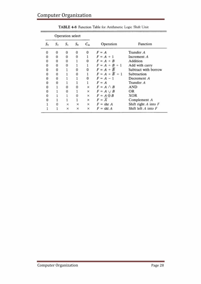
Arithmetic Logic Shift Unit
The arithmetic logic unit (ALU) is a common operational unit
connected to a number of storage registers To perform a microoperation, the contents of specified registers are
placed in the inputs of the ALU The ALU performs an operation and the result is then transferred to a
destination register The ALU is a combinational circuit so that the entire register transfer
operation from the source registers through the ALU and into the destination register can be performed during one clock pulse period
Computer Organization
Computer Organization Page 27
Computer Organization
Computer Organization Page 28
Computer Organization
Computer Organization Page 29
UNIT II Basic Computer Organization and Design
Instruction codes. Computer Registers Computer instructions, Timing and Control, Instruction cycle. Memory Reference Instructions, Input – Output and Interrupt, Complete Computer Description. Micro Programmed Control: Control memory, Address sequencing, micro program example, design of control unit, micro Programmed control ------------------------------------------------------------------------------------------------------------ Instruction Formats:
A computer will usually have a variety of instruction code formats. It
is the function of the control unit within the CPU to interpret each
instruction code and provide the necessary control functions needed to
process the instruction.
The format of an instruction is usually depicted in a rectangular box
symbolizing the bits of the instruction as they appear in memory words or in
a control register. The bits of the instruction are divided into groups called
fields. The most common fields found in instruction formats are:
1 An operation code field that specifies the operation to be performed. 2. An address field that designates a memory address or a processor
registers.
3. A mode field that specifies the way the operand or the effective address is determined.
Other special fields are sometimes employed under certain
circumstances, as for example a field that gives the number of shifts in a
shift-type instruction.
The operation code field of an instruction is a group of bits that define
various processor operations, such as add, subtract, complement, and shift.
The bits that define the mode field of an instruction code specify a variety
of alternatives for choosing the operands from the given address.
Operations specified by computer instructions are executed on some
data stored in memory or processor registers, Operands residing in
processor registers are specified with a register address. A register address
is a binary number of k bits that defines one of 2k registers in the CPU. Thus
a CPU with 16 processor registers R0 through R15 will have a register
address field of four bits. The binary number 0101, for example, will
Computer Organization
Computer Organization Page 30
designate register R5.
Computers may have instructions of several different lengths
containing varying number of addresses. The number of address fields in
the instruction format of a computer depends on the internal organization of
its registers. Most computers fall into one of three types of CPU
organizations: 1 Single accumulator organization.
2 General register organization.
3 Stack organization.
All operations are performed with an implied accumulator register.
The instruction format in this type of computer uses one address field. For
example, the instruction that specifies an arithmetic addition is defined by
an assembly language instruction as ADD.
Where X is the address of the operand. The ADD instruction in this
case results in the operation AC ← AC + M[X]. AC is the accumulator
register and M[X] symbolizes the memory word located at address X.
An example of a general register type of organization was presented
in Fig. 7.1. The instruction format in this type of computer needs three
register address fields. Thus the instruction for an arithmetic addition may
be written in an assembly language as
ADD R1, R2, R3
To denote the operation R1 ← R2 + R3. The number of address fields
in the instruction can be reduced from three to two if the destination register
is the same as one of the source registers. Thus the instruction
ADD R1, R2
Would denote the operation R1 ← R1 + R2. Only register addresses
for R1 and R2 need be specified in this instruction.
Computers with multiple processor registers use the move instruction
with a mnemonic MOV to symbolize a transfer instruction. Thus the
instruction
MOV R1, R2
Denotes the transfer R1 ← R2 (or R2 ← R1, depending on the
particular computer). Thus transfer-type instructions need two address fields
Computer Organization
Computer Organization Page 31
to specify the source and the destination.
General register-type computers employ two or three address fields in
their instruction format. Each address field may specify a processor register
or a memory word. An instruction symbolized by
ADD R1, X
Would specify the operation R1 ← R + M [X]. It has two address
fields, one for register R1 and the other for the memory address X.
The stack-organized CPU was presented in Fig. 8-4. Computers with
stack organization would have PUSH and POP instructions which require
an address field. Thus the instruction
PUSH X
Will push the word at address X to the top of the stack. The stack
pointer is updated automatically. Operation-type instructions do not need an
address field in stack-organized computers. This is because the operation is
performed on the two items that are on top of the stack. The instruction
ADD in a stack computer consists of an operation code only with no address
field. This operation has the effect of popping the two top numbers from the
stack, adding the numbers, and pushing the sum into the stack. There is no
need to specify operands with an address field since all operands are
implied to be in the stack.
To illustrate the influence of the number of addresses on computer
programs, we will evaluate the arithmetic statement X = (A + B) ∗ (C + D).
Using zero, one, two, or three address instruction. We will use the
symbols ADD, SUB, MUL, and DIV for the four arithmetic operations;
MOV for the transfer-type operation; and LOAD and STORE for transfers
to and from memory and AC register. We will assume that the operands are
in memory addresses A, B, C, and D, and the result must be stored in
memory at address X.
Three-Address Instructions Computers with three-address instruction formats can use each
address field to specify either a processor register or a memory operand.
The program in assembly language that evaluates X = (A + B) ∗ (C + D) is
shown below, together with comments that explain the register transfer
Computer Organization
Computer Organization Page 32
operation of each instruction.
ADD R1, A, B R1 ←
M [A] + M [B]
ADD R2, C, D R2 ←
M [C] + M [D]
MUL X, R1, R2 M [X]
← R1 ∗ R2
It is assumed that the computer has two processor registers, R1 and R2. The symbol M [A] denotes the operand at memory address symbolized by A. The advantage of the three-address format is that it results in short programs
when evaluating arithmetic expressions. The disadvantage is that the binary-
coded instructions require too many bits to specify three addresses. An
example of a commercial computer that uses three-address instructions is
the Cyber 170. The instruction formats in the Cyber computer are restricted
to either three register address fields or two register address fields and one
memory address field.
Two-Address Instructions Two address instructions are the most common in commercial computers.
Here again each address field can specify either a processor register or a
memory word. The program to evaluate X = (A + B) ∗ (C + D) is as
follows: MOV R1, A R1 ← M [A]
ADD R1, B R1 ← R1 + M [B]
MOV R2, C R2 ← M [C]
ADD R2, D R2 ← R2 + M [D]
MUL R1, R2 R1 ← R1∗R2
MOV X, R1 M [X] ← R1
The MOV instruction moves or transfers the operands to and from
memory and processor registers. The first symbol listed in an instruction is
assumed to be both a source and the destination where the result of the
operation is transferred.
Computer Organization
Computer Organization Page 33
One-Address Instructions One-address instructions use an implied accumulator (AC) register for
all data manipulation. For multiplication and division there is a need for a
second register. However, here we will neglect the second and assume that
the AC contains the result of tall operations. The program to evaluate X =
(A + B) ∗ (C + D) is
LOAD A AC ← M [A]
ADD B AC ← A [C] + M [B] STORE T M [T] ← AC
LOAD C AC ← M [C]
ADD D AC ← AC + M [D]
MUL T AC ← AC ∗ M [T]
STORE X M [X] ← AC
All operations are done between the AC register and a memory
operand. T is the address of a temporary memory location required for
storing the intermediate result.
Zero-Address Instructions A stack-organized computer does not use an address field for the
instructions ADD and MUL. The PUSH and POP instructions, however,
need an address field to specify the operand that communicates with the
stack. The following program shows how X = (A + B) ∗ (C + D) will be
written for a stack organized computer. (TOS stands for top of stack) PUSH A TOS ← A
PUSH B TOS ← B
ADD
PUSH
C
TOS ← (A + B)
TOS ← C
PUSH D TOS ← D
ADD TOS ← (C + D)
MUL
POP
X
TOS ← (C + D) ∗ (A + B)
M [X] ← TOS
To evaluate arithmetic expressions in a stack computer, it is necessary
to convert the expression into reverse Polish notation. The name “zero-
address” is given to this type of computer because of the absence of an
Computer Organization
Computer Organization Page 34
address field in the computational instructions.
Instruction Codes A set of instructions that specify the operations, operands, and the sequence by which processing has to occur. An instruction code is a group of bits that tells the computer to perform a specific operation part.
Format of Instruction The format of an instruction is depicted in a rectangular box symbolizing the bits of an instruction. Basic fields of an instruction format are given below: 1. An operation code field that specifies the operation to be performed. 2. An address field that designates the memory address or register. 3. A mode field that specifies the way the operand of effective address is
determined. Computers may have instructions of different lengths containing varying number of addresses. The number of address field in the instruction format depends upon the internal organization of its registers.
Addressing Modes To understand the various addressing modes to be presented in this section,
it is imperative that we understand the basic operation cycle of the computer.
The control unit of a computer is designed to go through an instruction cycle
that is divided into three major phases:
1. Fetch the instruction from memory 2. Decode the instruction.
3. Execute the instruction.
There is one register in the computer called the program counter of PC that
keeps track of the instructions in the program stored in memory. PC holds the
address of the instruction to be executed next and is incremented each time an
instruction is fetched from memory. The decoding done in step 2 determines
the operation to be performed, the addressing mode of the instruction and the
location of the operands. The computer then executes the instruction and
returns to step 1 to fetch the next instruction in sequence.
In some computers the addressing mode of the instruction is specified
with a distinct binary code, just like the operation code is specified. Other
computers use a single binary code that designates both the operation and
the mode of the instruction. Instructions may be defined with a variety of
Computer Organization
Computer Organization Page 35
addressing modes, and sometimes, two or more addressing modes are
combined in one instruction.
1. The operation code specified the operation to be performed. The
mode field is sued to locate the operands needed for the operation. There
may or may not be an address field in the instruction. If there is an address
field, it may designate a memory address or a processor register. Moreover,
as discussed in the preceding section, the instruction may have more than
one address field, and each address field may be associated with its own
particular addressing mode.
Although most addressing modes modify the address field of the
instruction, there are two modes that need no address field at all. These are
the implied and immediate modes. 1 Implied Mode: In this mode the operands are specified implicitly in the
definition of the instruction. For example, the instruction “complement accumulator” is
an implied-mode instruction because the operand in the accumulator register is implied
in the definition of the instruction. In fact, all register reference instructions that sue an
accumulator are implied-mode instructions.
Op code Mode Address
Figure 1: Instruction format with mode field
Zero-address instructions in a stack-organized computer are implied-
mode instructions since the operands are implied to be on top of the stack.
2 Immediate Mode: In this mode the operand is specified in the instruction
itself. Inother words, an immediate- mode instruction has an operand field rather than
an address field. The operand field contains the actual operand to be used in
conjunction with the operation specified in the instruction. Immediate-mode
instructions are useful for initializing registers to a constant value.
It was mentioned previously that the address field of an instruction
may specify either a memory word or a processor register. When the
address field specifies a processor register, the instruction is said to be in the
register mode.
3 Register Mode: In this mode the operands are in registers that reside within
the CPU.The particular register is selected from a register field in the instruction. A k-
bit field can specify any one of 2k registers.
4 Register Indirect Mode: In this mode the instruction specifies a register in the
CPUwhose contents give the address of the operand in memory. In other words, the
Computer Organization
Computer Organization Page 36
selected register contains the address of the operand rather than the operand itself.
Before using a register indirect mode instruction, the programmer must
ensure that the memory address fo the operand is placed in the processor
register with a previous instruction. A reference to the register is then
equivalent to specifying a memory address. The advantage of a register
indirect mode instruction is that the address field of the instruction sues
fewer bits to select a register than would have been required to specify a
memory address directly. 5 Auto increment or Auto decrement Mode: This is similar to the register indirect
modeexcept that the register is incremented or decremented after (or before) its value is
used to access memory. When the address stored in the register refers to a table of data
in memory, it is necessary to increment or decrement the register after every access to
the table. This can be achieved by using the increment or decrement instruction.
However, because it is such a common requirement, some computers incorporate a
special mode that automatically increments or decrements the content of the register
after data access.
The address field of an instruction is used by the control unit in the
CPU to obtain the operand from memory. Sometimes the value given in the
address field is the address of the operand, but sometimes it is just an
address from which the address of the operand is calculated. To differentiate
among the various addressing modes it is necessary to distinguish between
the address part of the instruction and the effective address used by the
control when executing the instruction. The effective address is defined to
be the memory address obtained from the computation dictated by the given
addressing mode. The effective address is the address of the operand in a
computational-type instruction. It is the address where control branches in
response to a branch-type instruction. We have already defined two
addressing modes in previous chapter.
6 Direct Address Mode: In this mode the effective address is equal to the address part
ofthe instruction. The operand resides in memory and its address is given directly by
the address field of the instruction. In a branch-type instruction the address field
specifies the actual branch address.
7 Indirect Address Mode: In this mode the address field of the instruction gives
theaddress where the effective address is stored in memory. Control fetches the
instruction from memory and uses its address part to access memory again to read the
Computer Organization
Computer Organization Page 37
effective address.
8 Relative Address Mode: In this mode the content of the program counter is added to
theaddress part of the instruction in order to obtain the effective address. The address
part of the instruction is usually a signed number (in 2‟s complement representation)
which can be either positive or negative. When this number is added to the content of
the program counter, the result produces an effective address whose position in
memory is relative to the address of the next instruction. To clarify with an example,
assume that the program counter contains the number 825 and the address part of the
instruction contains the number 24. The instruction at location 825 is read from
memory during the fetch phase and the program counter is then incremented by one
to 826 + 24 = 850. This is 24 memory locations forward from the address of the next
instruction. Relative addressing is often used with branch-type instructions when the
branch address is in the area surrounding the instruction word itself. It results in a
shorter address field in the instruction format since the relative address can be
specified with a smaller number of bits compared to the number of bits required to
designate the entire memory address.
9 Indexed Addressing Mode: In this mode the content of an index register is added
to theaddress part of the instruction to obtain the effective address. The index
register is a special CPU register that contains an index value. The address field of
the instruction defines the beginning address of a data array in memory. Each
operand in the array is stored in memory relative to the beginning address. The
distance between the beginning address and the address of the operand is the index
value stores in the index register. Any operand in the array can be accessed with
the same instruction provided that the index register contains the correct index
value. The index register can be incremented to facilitate access to consecutive
operands. Note that if an index-type instruction does not include an address field in
its format, the instructionconverts to the register indirect mode of operation. Some
computers dedicate one CPU register to function solely as an index register. This
register is involved implicitly when the index-mode instruction is used. In
computers with many processor registers, any one of the CPU registers can contain
the index number. In such a case the register must be specified explicitly in a
register field within the instruction format.
10 Base Register Addressing Mode: In this mode the content of a base register is
added tothe address part of the instruction to obtain the effective address. This is
similar to the indexed addressing mode except that the register is now called a base
register instead of an index register. The difference between the two modes is in
the way they are used rather than in the way that they are computed. An index
Computer Organization
Computer Organization Page 38
register is assumed to hold an index number that is relative to the address part of
the instruction. A base register is assumed to hold a base address and the address
field of the instruction gives a displacement relative to this base address. The base
register addressing mode is used in computers to facilitate the relocation of
programs in memory. When programs and data are moved from one segment of
memory to another, as required in multiprogramming systems, the address values
of the base register requires updating to reflect the beginning of a new memory
segment.
Numerical Example
Computer Organization
Computer Organization Page 39
Computer Registers
Data Register(DR) : hold the operand(Data) read from memory
Accumulator Register(AC) : general purpose processing register
Instruction Register(IR) : hold the instruction read from memory
Temporary Register(TR) : hold a temporary data during processing
Address Register(AR) : hold a memory address, 12 bit width
Program Counter(PC) : »hold the address of the next instruction to be read from memory after the current instruction is executed »Instruction words are read and executed in sequence unless a branch instruction is encountered »A branch instruction calls for a transfer to a nonconsecutive instruction in the program »The address part of a branch instruction is transferred to PC to become the address of the next instruction Input Register(INPR) : receive an 8-bit character from an input device
Output Register(OUTR) : hold an 8-bit character for an output device The following registers are used in Mano‟s example computer.
Register Number Register Register
symbol of bits name Function-----------------------
DR 16 Data register Holds memory operands
AR 12 Address register Holds address for memory
AC 16 Accumulator Processor register
IR 16 Instruction register Holds instruction code
PC 12 Program counter Holds address of instruction
TR 16 Temporary register Holds temporary data
INPR 8 Input register Holds input character
OUTR 8 Output register Holds output character
Computer Organization
Computer Organization Page 40
Computer Instructions: The basic computer has 16 bit instruction register (IR) which can denote either memory reference or register reference or input-output instruction.
1. Memory Reference – These instructions refer to memory address as an operand. The other operand is always accumulator. Specifies 12 bit address, 3 bit opcode (other than 111) and 1 bit addressing mode for direct and indirect addressing. Example – IR register contains = 0001XXXXXXXXXXXX, i.e. ADD after fetching and decoding of instruction we find out that it is a memory reference instruction for ADD operation.
Hence, DR <- M[AR] AC <- AC+ DR, SC <- 0
2. Register Reference – These instructions perform operations on registers rather than memory addresses. The IR(14-12) is 111 (differentiates it from memory reference) and IR(15) is 0 (differentiates it from input/output instructions). The rest 12 bits specify register operation. Example – IR register contains = 0111001000000000, i.e. CMA after fetch and decode cycle we find out that it is a register reference instruction for complement accumulator.
Hence, AC <- ~AC
3. Input/Output – These instructions are for communication between computer and outside environment. The IR(14-12) is 111 (differentiates it from memory reference) and IR(15) is 1 (differentiates it from register reference instructions). The rest 12 bits specify I/O operation. Example – IR register contains = 1111100000000000, i.e. INP after fetch and decode cycle we find out that it is an input/output instruction for inputing character. Hence, INPUT character from peripheral device.
Timing and Control
All sequential circuits in the Basic Computer CPU are driven by a master clock, with the exception of the INPR register. At each clock pulse, the control unit sends control signals to control inputs of the bus, the registers, and the ALU. Control unit design and implementation can be done by two general methods:
A hardwired control unit is designed from scratch using traditional digital logic design techniques to produce a minimal, optimized circuit. In other words, the control unit is like an ASIC (application-specific integrated circuit).
A microprogrammed control unit is built from some sort of ROM. The desired control signals are simply stored in the ROM, and retrieved in sequence to drive the microoperations needed by a particular instruction.
Computer Organization
Computer Organization Page 41
Instruction Cycle
The CPU performs a sequence of microoperations for each instruction. The sequence for each instruction of the Basic Computer can be refined into 4 abstract phases:
Program execution can be represented as a top-down design:
1. Program execution a. Instruction 1
i. Fetch instruction ii. Decode
iii. Fetch operand iv. Execute
b. Instruction 2 i. Fetch instruction
ii. Decode iii. Fetch operand iv. Execute
c. Instruction 3 ...
Program execution begins with:
PC ← address of first instruction, SC ← 0
After this, the SC is incremented at each clock cycle until an instruction is completed, and then it is cleared to begin the next instruction. This process repeats until a HLT instruction is executed, or until the power is shut off.
Instruction Fetch and Decode The instruction fetch and decode phases are the same for all instructions, so the control functions and microoperations will be independent of the instruction code. Everything that happens in this phase is driven entirely by timing variables T0, T1 and T2. Hence, all control inputs in the CPU during fetch and decode are functions of these three variables alone.
T0: AR ← PC
T1: IR ← M[AR], PC ← PC + 1
T2: D0-7 ← decoded IR(12-14), AR ← IR(0-11), I ← IR(15)
For every timing cycle, we assume SC ← SC + 1 unless it is stated that SC ← 0.
Computer Organization
Computer Organization Page 42
Micro Programmed Control: Control Memory The control unit in a digital computer initiates sequences of microoperations The complexity of the digital system is derived form the number of
sequences that are performed When the control signals are generated by hardware, it is hardwired In a bus-oriented system, the control signals that specify
microoperations are groups of bits that select the paths in multiplexers, decoders, and ALUs.
The control unit initiates a series of sequential steps of microoperations The control variables can be represented by a string of 1‟s and 0‟s called a
control word A microprogrammed control unit is a control unit whose binary control
variables are stored in memory A sequence of microinstructions constitutes a microprogram The control memory can be a read-only memory Dynamic microprogramming permits a microprogram to be loaded
and uses a writable control memory A computer with a microprogrammed control unit will have two
separate memories: a main memory and a control memory The microprogram consists of microinstructions that specify various
internal control signals for execution of register microoperations These microinstructions generate the microoperations to:
o fetch the instruction from main memory o evaluate the effective address o execute the operation o return control to the fetch phase for the next instruction
The control memory address register specifies the address of the microinstruction
The control data register holds the microinstruction read from memory The microinstruction contains a control word that specifies one
or more microoperations for the data processor The location for the next microinstruction may, or may not be the
next in sequence Some bits of the present microinstruction control the generation of the
address of the next microinstruction The next address may also be a function of external input conditions While the microoperations are being executed, the next address is
computed in the next address generator circuit (sequencer) and then transferred into the CAR to read the next microinstructions
Typical functions of a sequencer are: o incrementing the CAR by one o loading into the CAR and address from control memory o transferring an external address o loading an initial address to start the control operations
A clock is applied to the CAR and the control word and next-address
Computer Organization
Computer Organization Page 43
information are taken directly from the control memory The address value is the input for the ROM and the control work is the
output No read signal is required for the ROM as in a RAM
The main advantage of the microprogrammed control is that once the
hardware configuration is established, there should be no need for h/w or wiring changes
To establish a different control sequence, specify a different set of microinstructions for control memory
Address Sequencing
Microinstructions are stored in control memory in groups, with each group
specifying a routine Each computer instruction has its own microprogram routine to
generate the microoperations The hardware that controls the address sequencing of the control memory
must be capable of sequencing the microinstructions within a routine and be able to branch from one routine to another
Steps the control must undergo during the execution of a single computer instruction:
o Load an initial address into the CAR when power is turned on in the computer. This address is usually the address of the first microinstruction that activates the instruction fetch routine – IR holds instruction
o The control memory then goes through the routine to determine the effective address of the operand – AR holds operand address
o The next step is to generate the microoperations that execute the instruction by considering the opcode and applying a mapping
o After execution, control must return to the fetch routine by executing an unconditional branch
The microinstruction in control memory contains a set of bits to initiate microoperations in computer registers and other bits to specify the method by which the next address is obtained
Conditional branching is obtained by using part of the microinstruction to select a specific status bit in order to determine its condition
The status conditions are special bits in the system that provide parameter information such as the carry-out of an adder, the sign bit of a number, the mode bits of an instruction, and i/o status conditions
The status bits, together with the field in the microinstruction that specifies a branch address, control the branch logic
The branch logic tests the condition, if met then branches, otherwise, increments the CAR
If there are 8 status bit conditions, then 3 bits in the microinstruction are used to specify the condition and provide the selection variables for the multiplexer
Computer Organization
Computer Organization Page 44
For unconditional branching, fix the value of one status bit to be one load the branch address from control memory into the CAR
A special type of branch exists when a microinstruction specifies a branch to the first word in control memory where a microprogram routine is located
The status bits for this type of branch are the bits in the opcode Assume an opcode of four bits and a control memory of 128 locations The mapping process converts the 4-bit opcode to a 7-bit address for
control memory This provides for each computer instruction a microprogram routine
with a capacity of four microinstructions
Subroutines are programs that are used by other routines to accomplish a particular task and can be called from any point within the main body of the microprogram
Frequently many microprograms contain identical section of code Microinstructions can be saved by employing subroutines that use
common sections of microcode Microprograms that use subroutines must have a provisions for storing
the return address during a subroutine call and restoring the address during a subroutine return
A subroutine register is used as the source and destination for the addresses
Computer Organization
Computer Organization Page 45
UNIT III Computer Processing Unit Organization
Introduction to CPU
The operation or task that must perform by CPU is: • Fetch Instruction: The CPU reads an instruction from memory. • Interpret Instruction: The instruction is decoded to determine what action is required. • Fetch Data: The execution of an instruction may require reading data from memory or I/O module. • Process data: The execution of an instruction may require performing some arithmetic or logical operation on data. • Write data: The result of an execution may require writing data to memory or an I/O module. To do these tasks, it should be clear that the CPU needs to store some data temporarily. It must remember the location of the last instruction so that it can know where to get the next instruction. It needs to store instructions and data temporarily while an instruction is being executed. In other words, the CPU needs a small internal memory. These storage locations are generally referred as registers. The major components of the CPU are an arithmetic and logic unit (ALU) and a control unit (CU). The ALU does the actual computation or processing of data. The CU controls the movement of data and instruction into and out of the CPU and controls the operation of the ALU. The CPU is connected to the rest of the system through system bus. Through system bus, data or information gets transferred between the CPU and the other component of the system. The system bus may have three components: Data Bus: Data bus is used to transfer the data between main memory and CPU. Address Bus: Address bus is used to access a particular memory location by putting the address of the memory location. Control Bus: Control bus is used to provide the different control signal generated by CPU to different part of the system. As for example, memory read is a signal generated by CPU to indicate that a memory read operation has to be performed. Through control bus this signal is transferred to memory module to indicate the required operation.
Figure 1: CPU with the system bus.
There are three basic components of CPU: register bank, ALU and Control Unit. There
Computer Organization
Computer Organization Page 46
are several data movements between these units and for that an internal CPU bus is used. Internal CPU bus is needed to transfer data between the various registers and the ALU.
Figure 2 : Internal Structure of CPU Stack Organization: A useful feature that is included in the CPU of most computers is a stack or last in, first out (LIFO) list. A stack is a storage device that stores information in such a manner that the item stored last is the first item retrieved. The operation of a stack can be compared to a stack of trays. The last tray placed on top of the stack is the first to be taken off. The stack in digital computers is essentially a memory unit with an address register that can only( after an initial value is loaded in to it).The register that hold the address for the stack is called a stack pointer (SP) because its value always points at the top item in stack. Contrary to a stack of trays where the tray it self may be taken out or inserted, the physical registers of a stack are always available for reading or writing. The two operation of stack are the insertion and deletion of items. The operation of insertion is called PUSH because it can be thought of as the result of pushing a new item on top. The operation of deletion is called POP because it can be thought of as the result of removing one item so that the stack pops up. However, nothing is pushed or popped in a computer stack. These operations are simulated by incrementing or decrementing the stack pointer register.
Computer Organization
Computer Organization Page 47
Register stack: A stack can be placed in a portion of a large memory or it can be organized as a collection of a finite number of memory words or registers. Figure X shows the organization of a 64-word register stack. The stack pointer register SP contains a binary number whose value is equal to the address of the word that is currently on top of the stack. Three items are placed in the stack: A, B, and C in the order. item C is on the top of the stack so that the content of sp is now 3. To remove the top item, the stack is popped by reading the memory word at address 3 and decrementing the content of SP. Item B is now on top of the stack since SP holds address 2. To insert a new item, the stack is pushed by incrementing SP and writing a word in the next higher location in the stack. Note that item C has read out but not physically removed. This does not matter because when the stack is pushed, a new item is written in its place. In a 64-word stack, the stack pointer contains 6 bits because 26 =64. since SP has only six bits, it cannot exceed a number grater than 63(111111 in binary). When 63 is incremented by 1, the result is 0 since 111111 + 1 =1000000 in binary, but SP can accommodate only the six least significant bits. Similarly, when 000000 is decremented by 1, the result is 111111. The one bit register Full is set to 1 when the stack is full, and the one-bit register EMTY is set to 1 when the stack is empty of items. DR is the data register that holds the binary data to be written in to or read out of the stack.
Figure 3: Block Diagram Of A 64-Word Stack Initially, SP is cleared to 0, Emty is set to 1, and Full is cleared to 0, so that SP points to the word at address o and the stack is marked empty and not full. if the stack is not full , a new item is inserted with a push operation. the push operation is implemented with the following sequence of micro-operation. SP ←SP + 1 (Increment stack pointer) M(SP) ← DR (Write item on top of the stack) if (sp=0) then (Full ← 1) (Check if stack is full) Emty ← 0 ( Marked the stack not empty)
Computer Organization
Computer Organization Page 48
The stac pointer is incremented so that it points to the address of the next-higher word. A memory write operation inserts the word from DR into the top of the stack. Note that SP holds the address of the top of the stack and that M(SP) denotes the memory word specified by the address presently available in SP, the first item stored in the stack is at address 1. The last item is stored at address 0, if SP reaches 0, the stack is full of item, so FULLL is set to 1. This condition is reached if the top item prior to the last push was in location 63 and after increment SP, the last item stored in location 0. Once an item is stored in location 0, there are no more empty register in the stack. If an item is written in the stack, Obviously the stack can not be empty, so EMTY is cleared to 0. DR← M[SP] Read item from the top of stack SP ← SP-1 Decrement stack Pointer if( SP=0) then (Emty ← 1) Check if stack is empty FULL ← 0 Mark the stack not full The top item is read from the stack into DR. The stack pointer is then decremented. if its value reaches zero, the stack is empty, so Emty is set to 1. This condition is reached if the item read was in location 1. once this item is read out , SP is decremented and reaches the value 0, which is the initial value of SP. Note that if a pop operation reads the item from location 0 and then SP is decremented, SP changes to 111111, which is equal to decimal 63. In this configuration, the word in address 0 receives the last item in the stack. Note also that an erroneous operation will result if the stack is pushed when FULL=1 or popped when EMTY =1. Memory Stack : A stack can exist as a stand-alone unit as in figure 4 or can be implemented in a random access memory attached to CPU. The implementation of a stack in the CPU is done by assigning a portion of memory to a stack operation and using a processor register as a stack pointer. Figure shows a portion of computer memory partitioned in to three segment program, data and stack. The program counter PC points at the address of the next instruction in the program. The address register AR points at an array of data. The stack pointer SP points at the top of the stack. The three register are connected to a common address bus, and either one can provide an address for memory. PC is used during the fetch phase to read an instruction. AR is used during the execute phase to read an operand. SP is used to push or POP items into or from the stack. As show in figure :4 the initial value of SP is 4001 and the stack grows with decreasing addresses. Thus the first item stored in the stack is at address 4000, the second item is stored at address 3999, and the last address hat can be used for the stack is 3000. No previous are available for stack limit checks. We assume that the items in the stack communicate with a data register DR. A new item is inserted with the push operation as follows. SP← SP-1 M[SP] ← DR The stack pointer is decremented so that it points at the address of the next word. A Memory write operation insertion the word from DR into the top of the stack. A new item is deleted with a pop operation as follows. DR← M[SP] SP←SP + 1 The top item is read from the stack in to DR. The stack pointer is then incremented to point at the next item in the stack. Most computer do not provide hardware to check for stack overflow (FULL) or underflow (Empty). The stack limit can be checked by using two prossor register :
Computer Organization
Computer Organization Page 49
one to hold upper limit and other hold the lower limit. after the pop or push operation SP is compared with lower or upper limit register.
Figure 4: computer memory with program, data and stack segments INSTRUCTION FORMATS: We know that a machine instruction has an opcode and zero or more operands. Encoding an instruction set can be done in a variety of ways. Architectures are differentiated from one another by the number of bits allowed per instruction (16, 32, and 64 are the most common), by the number of operands allowed per instruction, and by the types of instructions and data each can process. More specifically, instruction sets are differentiated by the following features: 1. Operand storage in the CPU (data can be stored in a stack structure or in registers) 2. Number of explicit operands per instruction (zero, one, two, and three being the most common) 3. Operand location (instructions can be classified as register-to-register, register-to-memory or memory-to-memory, which simply refer to the combinations of operands allowed per instruction) 4. Operations (including not only types of operations but also which instructions can access memory and which cannot) 5. Type and size of operands (operands can be addresses, numbers, or even characters) Number of Addresses: One of the characteristics of the ISA(Industrial Standard Architecture) that shapes the architecture is the number of addresses used in an instruction. Most operations can be divided into binary or unary operations. Binary operations such as addition and
Computer Organization
Computer Organization Page 50
multiplication require two input operands whereas the unary operations such as the logical NOT need only a single operand. Most operations produce a single result. There are exceptions, however. For example, the division operation produces two outputs: a quotient and a remainder. Since most operations are binary, we need a total of three addresses: two addresses to specify the two input operands and one to specify where the result should go. Three-Address Machines: In three-address machines, instructions carry all three addresses explicitly. The RISC processors use three addresses. Table X1 gives some sample instructions of a three-address machine. In these machines, the C statement A = B + C * D - E + F + A is converted to the following code: mult T,C,D ; T = C*D add T,T,B ; T = B + C*D sub T,T,E ; T = B + C*D - E add T,T,F ; T = B + C*D - E + F add A,T,A ; A = B + C*D - E + F + A Table :T1 Sample three-address machine instructions Instruction
Semantics
add dest,src1,src2 Adds the two values at src1 and src2 and stores the result in dest M(dest) = [src1] + [src2]
sub dest,src1,src2 Subtracts the second source operand at src2 from the first at src1 and stores the result in dest M(dest) = [src1] - [src2]
mult dest,src1,src2 Multiplies the two values at src1 and src2 and stores the result in dest M(dest) = [src1] * [src2]
We use the notation that each variable represents a memory address that stores the value associated with that variable. This translation from symbol name to the memory address is done by using a symbol table. As you can see from this code, there is one instruction for each arithmetic operation. Also notice that all instructions, barring the first one, use an address twice. In the middle three instructions, it is the temporary T and in the last one, it is A. This is the motivation for using two addresses, as we show next. Two-Address Machines : In two-address machines, one address doubles as a source and destination. Usually, we use dest to indicate that the address is used for destination. But you should note that this address also supplies one of the source operands. The Pentium is an example processor that uses two addresses. Sample instructions of a two-address machine On these machines, the C statement
Computer Organization
Computer Organization Page 51
A = B + C * D - E + F + A is converted to the following code: load T,C ; T = C mult T,D ; T = C*D add T,B ; T = B + C*D sub T,E ; T = B + C*D - E add T,F ; T = B + C*D - E + F add A,T ; A = B + C*D - E + F + A Table :T2 Sample Two-address machine instructions: Instruction
Semantics
load dest,src Copies the value at src to dest M(dest) = [src]
add dest,src Adds the two values at src and dest and stores the result in dest M(dest) = [dest] + [src]
sub dest,src Subtracts the second source operand at src from the first at dest and stores the result in dest M(dest) = [dest] - [src]
mult dest,src Multiplies the two values at src and dest and stores the result in dest M(dest) = [dest] * [src]
Since we use only two addresses, we use a load instruction to first copy the C value into a temporary represented by T. If you look at these six instructions, you will notice that the operand T is common. If we make this our default, then we don‟t need even two addresses: we can get away with just one address. One-Address Machines : In the early machines, when memory was expensive and slow, a special set of registers was used to provide an input operand as well as to receive the result from the ALU. Because of this, these registers are called the accumulators. In most machines, there is just a single accumulator register. This kind of design, called accumulator machines, makes sense if memory is expensive. In accumulator machines, most operations are performed on the contents of the accumulator and the operand supplied by the instruction. Thus, instructions for these machines need to specify only the address of a single operand. There is no need to store the result in memory: this reduces the need for larger memory as well as speeds up the computation by reducing the number of memory accesses. A few sample accumulator machine instructions are shown in Table X3. In these machines, the C statement A = B + C * D - E + F + A is converted to the following code: load C ; load C into the accumulator mult D ; accumulator = C*D add B ; accumulator = C*D+B sub E ; accumulator = C*D+B-E add F ; accumulator = C*D+B-E+F
Computer Organization
Computer Organization Page 52
add A ; accumulator = C*D+B-E+F+A store A ; store the accumulator contents in A
load addr Copies the value at address addr into the accumulator accumulator = [addr]
store addr Stores the value in the accumulator at the memory address addr M(addr) = accumulator
add addr Adds the contents of the accumulator and value at address addr accumulator = accumulator + [addr]
sub addr Subtracts the value at memory address addr from the contents of the accumulator accumulator = accumulator - [addr]
mult addr Multiplies the contents of the accumulator and value at address addr accumulator = accumulator * [addr]
Zero-Address Machines : In zero-address machines, locations of both operands are assumed to be at a
default location. These machines use the stack as the source of the input operands and the result goes back into the stack. Stack is a LIFO (last-in-first-out) data structure that all processors support, whether or not they are zero-address machines. As the name implies, the last item placed on the stack is the first item to be taken out of the stack. A good analogy is the stack of trays you find in a cafeteria.
All operations on this type of machine assume that the required input operands are the top two values on the stack. The result of the operation is placed on top of the stack. Table X4 gives some sample instructions for the stack machines.
push addr Places the value at address addr on top of the stack push([addr])
pop addr Stores the top value on the stack at memory address addr M(addr) = pop
add Adds the top two values on the stack and pushes the result onto the stack push(pop + pop)
sub Subtracts the second top value from the top value of the stack and pushes the result onto the stack push(pop – pop)
mult Multiplies the top two values in the stack and pushes the result onto the stack push(pop * pop)
Notice that the first two instructions are not zero-address instructions. These
Computer Organization
Computer Organization Page 53
two are special instructions that use a single address and are used to move data between memory and stack.
All other instructions use the zero-address format. Let‟s see how the stack machine translates the arithmetic expression we have seen in the previous subsections. In these machines, the C statement
A = B + C * D - E + F + A is converted to the following code:
push E ; <E> push C ; <C, E> push D ; <D, C, E> mult ; <C*D, E> push B ; <B, C*D, E> add ; <B+C*D, E> sub ; <B+C*D-E> push F ; <F, B+D*C-E> add ; <F+B+D*C-E> push A ; <A, F+B+D*C-E> add ; <A+F+B+D*C-E> pop A ; < >
On the right, we show the state of the stack after executing each instruction.
The top element of the stack is shown on the left. Notice that we pushed E early because we need to subtract it from (B+C*D).
Stack machines are implemented by making the top portion of the stack internal to the processor. This is referred to as the stack depth. The rest of the stack is placed in memory. Thus, to access the top values that are within the stack depth, we do not have to access the memory. Obviously, we get better performance by increasing the stack depth.
INSTRUCTION TYPES
Most computer instructions operate on data; however, there are some that do not. Computer manufacturers regularly group instructions into the following categories: • Data movement • Arithmetic • Boolean • Bit manipulation (shift and rotate) • I/O • Transfer of control • Special purpose
Data movement instructions are the most frequently used instructions. Data is moved from memory into registers, from registers to registers, and from registers to memory, and many machines provide different instructions depending on the source and destination. For example, there may be a MOVER instruction that always requires two register operands, whereas a MOVE instruction allows one register and one memory operand.
Computer Organization
Computer Organization Page 54
Some architectures, such as RISC, limit the instructions that can move data to and from memory in an attempt to speed up execution. Many machines have ariations of load, store, and move instructions to handle data of different sizes. For example, there may be a LOADB instruction for dealing with bytes and a LOADW instruction for handling words.
Arithmetic operations include those instructions that use integers and floating point numbers. Many instruction sets provide different arithmetic instructions for various data sizes. As with the data movement instructions, there are sometimes different instructions for providing various combinations of register and memory accesses in different addressing modes.
Boolean logic instructions perform Boolean operations, much in the same way that arithmetic operations work. There are typically instructions for performing AND, NOT, and often OR and XOR operations.
Bit manipulation instructions are used for setting and resetting individual bits
(or sometimes groups of bits) within a given data word. These include both arithmetic and logical shift instructions and rotate instructions, both to the left and to the right. Logical shift instructions simply shift bits to either the left or the right by a specified amount, shifting in zeros from the opposite end. Arithmetic shift instructions, commonly used to multiply or divide by 2, do not shift the leftmost bit, because this represents the sign of the number. On a right arithmetic shift, the sign bit is replicated into the bit position to its right. On a left arithmetic shift, values are shifted left, zeros are shifted in, but the sign bit is never moved. Rotate instructions are simply shift instructions that shift in the bits that are shifted out. For example, on a rotate left 1 bit, the leftmost bit is shifted out and rotated around to become the rightmost bit.
I/O instructions vary greatly from architecture to architecture. The basic
schemes for handling I/O are programmed I/O, interrupt-driven I/O, and DMA devices. These are covered in more detail in Chapter 5.
Control instructions include branches, skips, and procedure calls. Branching
can be unconditional or conditional. Skip instructions are basically branch instructions with implied addresses. Because no operand is required, skip instructions often use bits of the address field to specify different situations (recall the Skipcond instruction used by MARIE). Procedure calls are special branch instructions that automatically save the return address. Different machines use different methods to save this address. Some store the address at a specific location in memory, others store it in a register, while still others push the return address on a stack. We have already seen that stacks can be used for other purposes.
Special purpose instructions include those used for string processing, high
level language support, protection, flag control, and cache management. Most architectures provide instructions for string processing, including string manipulation and searching. Addressing Modes
We have examined the types of operands and operations that may be specified by machine instructions. Now we have to see how is the address of an operand specified, and how are the bits of an instruction organized to define the operand addresses and operation of that instruction.
Computer Organization
Computer Organization Page 55
Addressing Modes: The most common addressing techniques are
• Immediate • Direct • Indirect • Register • Register Indirect • Displacement • Stack All computer architectures provide more than one of these addressing modes.
The question arises as to how the control unit can determine which addressing mode is being used in a particular instruction. Several approaches are used. Often, different opcodes will use different addressing modes. Also, one or more bits in the instruction format can be used as a mode field. The value of the mode field determines which addressing mode is to be used.
What is the interpretation of effective address. In a system without virtual memory, the effective address will be either a main memory address or a register. In a virtual memory system, the effective address is a virtual address or a register. The actual mapping to a physical address is a function of the paging mechanism and is invisible to the programmer. To explain the addressing modes, we use the following notation:
A = contents of an address field in the instruction that refers to a
memory
R = contents of an address field in the instruction that refers to a
register
EA = actual (effective) address of the location containing the
referenced operand
(X) = contents of location X
Immediate Addressing: The simplest form of addressing is immediate addressing, in which the
operand is actually present in the instruction: OPERAND = A
This mode can be used to define and use constants or set initial values of variables. The advantage of immediate addressing is that no memory reference other than the instruction fetch is required to obtain the operand. The disadvantage is that the size of the number is restricted to the size of the address field, which, in most instruction sets, is small compared with the world length.
Computer Organization
Computer Organization Page 56
Figure 4.1: Immediate Addressing Mod
The instruction format for Immediate Addressing Mode is shown in the Figure 4.1. Direct Addressing:
A very simple form of addressing is direct addressing, in which the address field contains the effective address of the operand:
EA = A It requires only one memory reference and no special calculation.
Figure 4.2: Direct Addressing Mode Indirect Addressing:
With direct addressing, the length of the address field is usually less than the word length, thus limiting the address range. One solution is to have the address field refer to the address of a word in memory, which in turn contains a full-length address of the operand. This is know as indirect addressing:
Register addressing is similar to direct addressing. The only difference is that the address field refers to a register rather than a main memory address:
EA = R
Computer Organization
Computer Organization Page 57
The advantages of register addressing are that only a small address field is
needed in the instruction and no memory reference is required. The disadvantage of register addressing is that the address space is very limited.
Figure 4.4: Register Addressing Mode.
The exact register location of the operand in case of Register Addressing Mode is shown in the Figure 34.4. Here, 'R' indicates a register where the operand is present. Register Indirect Addressing:
Register indirect addressing is similar to indirect addressing, except that the address field refers to a register instead of a memory location. It requires only one memory reference and no special calculation.
EA = (R) Register indirect addressing uses one less memory reference than indirect
addressing. Because, the first information is available in a register which is nothing but a memory address. From that memory location, we use to get the data or information. In general, register access is much more faster than the memory access.
Computer Organization
Computer Organization Page 58
Diaplacement Addressing: A very powerful mode of addressing combines the capabilities of direct
addressing and register indirect addressing, which is broadly categorized as displacement addressing:
EA = A + (R) Displacement addressing requires that the instruction have two address fields, at
least one of which is explicit. The value contained in one address field (value = A) is used directly. The other address field, or an implicit reference based on opcode, refers to a register whose contents are added to A to produce the effective address. The general format of Displacement Addressing is shown in the Figure 4.6. Three of the most common use of displacement addressing are:
For relative addressing, the implicitly referenced register is the program counter (PC). That is, the current instruction address is added to the address field to produce the EA. Thus, the effective address is a displacement relative to the address of the instruction. Base-Register Addressing:
The reference register contains a memory address, and the address field contains a displacement from that address. The register reference may be explicit or implicit. In some implementation, a single segment/base register is employed and is used implicitly. In others, the programmer may choose a register to hold the base address of a segment, and the instruction must reference it explicitly. Indexing:
The address field references a main memory address, and the reference register contains a positive displacement from that address. In this case also the register reference is sometimes explicit and sometimes implicit.
Generally index register are used for iterative tasks, it is typical that there is a need to increment or decrement the index register after each reference to it. Because
Computer Organization
Computer Organization Page 59
this is such a common operation, some system will automatically do this as part of the same instruction cycle. This is known as auto-indexing. We may get two types of auto-indexing: -one is auto-incrementing and the other one is -auto-decrementing.
If certain registers are devoted exclusively to indexing, then auto-indexing can be invoked implicitly and automatically. If general purpose register are used, the auto index operation may need to be signaled by a bit in the instruction. Auto-indexing using increment can be depicted as follows:
EA = A + (R) R = (R) + 1
Auto-indexing using decrement can be depicted as follows:
EA = A + (R) R = (R) - 1
In some machines, both indirect addressing and indexing are provided, and it is possible to employ both in the
same instruction. There are two possibilities: The indexing is performed either before or after the indirection. If indexing is performed after the indirection, it is termed post indexing EA = (A) + (R)
First, the contents of the address field are used to access a memory location containing an address. This address is then indexed by the register value. With pre indexing, the indexing is performed before the indirection: EA = ( A + (R)
An address is calculated, the calculated address contains not the operand, but the address of the operand. Stack Addressing:
A stack is a linear array or list of locations. It is sometimes referred to as a pushdown list or last-in- first-out queue. A stack is a reserved block of locations. Items are appended to the top of the stack so that, at any given time, the block is partially filled. Associated with the stack is a pointer whose value is the address of the top of the stack. The stack pointer is maintained in a register. Thus, references to stack locations in memory are in fact register indirect addresses.
The stack mode of addressing is a form of implied addressing. The machine instructions need not include a memory reference but implicitly operate on the top of the stack.
Computer Organization
Computer Organization Page 60
COMPUTER ARITHMETIC
Introduction:
Data is manipulated by using the arithmetic instructions in digital computers. Data is manipulated to produce results necessary to give solution for the computation problems. The Addition, subtraction, multiplication and division are the four basic arithmetic operations. If we want then we can derive other operations by using these four operations.
To execute arithmetic operations there is a separate section called arithmetic processing unit in central processing unit. The arithmetic instructions are performed generally on binary or decimal data. Fixed-point numbers are used to represent integers or fractions. We can have signed or unsigned negative numbers. Fixed-point addition is the simplest arithmetic operation.
If we want to solve a problem then we use a sequence of well-defined steps. These steps are collectively called algorithm. To solve various problems we give algorithms.
In order to solve the computational problems, arithmetic instructions are used in digital computers that manipulate data. These instructions perform arithmetic calculations.
And these instructions perform a great activity in processing data in a digital computer. As we already stated that with the four basic arithmetic operations addition, subtraction, multiplication and division, it is possible to derive other arithmetic operations and solve scientific problems by means of numerical analysis methods.
A processor has an arithmetic processor(as a sub part of it) that executes arithmetic operations. The data type, assumed to reside in processor, registers during the execution of an arithmetic instruction. Negative numbers may be in a signed magnitude or signed complement representation. There are three ways of representing negative fixed point - binary numbers signed magnitude, signed 1‟s complement or signed 2‟s complement. Most computers use the signed magnitude representation for the mantissa.
Addition and Subtraction :
Addition and Subtraction with Signed –Magnitude Data
We designate the magnitude of the two numbers by A and B. Where the signed numbers are added or subtracted, we find that there are eight different conditions to consider, depending on the sign of the numbers and the operation performed. These conditions are listed in the first column of Table 4.1. The other columns in the table show the actual operation to be performed with the magnitude of the numbers. The last column is needed to present a negative zero. In other words, when two equal numbers are subtracted, the result should be +0 not -0. The algorithms for addition and subtraction are derived from the table and can be stated as follows (the words parentheses should be used for the subtraction algorithm).
Addition and Subtraction of Signed-Magnitude Numbers
Computer Organization
Computer Organization Page 61
Computer Arithmetic Addition and Subtraction
SIGNED MAGNITUDEADDITION AND SUBTRACTION
Addition: A + B ; A: Augend; B: Addend Subtraction: A - B: A: Minuend; B: Subtrahend
Hardware Implementation Bs B Register
AVF Complementer M(Mode Control)
E Output Parallel Adder Input Carry Carry S
As A Register Load Sum
Computer Arithmetic Addition and Subtraction
Algorithm:
The flowchart is shown in Figure 7.1. The two signs A, and B, are compared by an exclusive-OR gate.
If the output of the gate is 0 the signs are identical; If it is 1, the signs are different.
END END
Augend in AC Addend in B
Add Subtract Algorithm
V Overflow
Hardware
SIGNED 2’S COMPLEMENT ADDITION AND SUBTRACTION
AC AC + B V overflow
AC AC + B’+ 1 V overflow
Minuend in AC Subtrahend in B
AC
Complementer and Parallel Adder
B Register
Operation
Add Magnitude
Subtract Magnitude When A>B When A<B When A=B
(+A) + (+B) (+A) + (- B) (- A) + (+B) (- A) + (- B) (+A) - (+B) (+A) - (- B) (- A) - (+B) (- A) - (- B)
+(A + B)
- (A + B)
+(A + B) - (A + B)
+(A - B) - (A - B)
+(A - B)
- (A - B)
- (B - A) +(B - A)
- (B - A)
+(B - A)
+(A - B) +(A - B)
+(A - B)
+(A - B)
Computer Organization
Computer Organization Page 62
For an add operation, identical signs dictate that the magnitudes be added. For a subtract operation, different signs dictate that the magnitudes be added.
The magnitudes are added with a microoperation EA A + B, where EA is a register that combines E and A. The carry in E after the addition constitutes an overflow if it is equal to 1. The value of E is transferred into the add-overflow flip-flop AVF.
The two magnitudes are subtracted if the signs are different for an add operation or identical for a subtract operation. The magnitudes are subtracted by adding A to the 2's complemented B. No overflow can occur if the numbers are subtracted so AVF is cleared to 0.
1 in E indicates that A >= B and the number in A is the correct result. If this numbs is zero, the sign A must be made positive to avoid a negative zero.
0 in E indicates that A < B. For this case it is necessary to take the 2's complement of the value in A. The operation can be done with one microoperation A A' +1.
However, we assume that the A register has circuits for microoperations complement and increment, so the 2's complement is obtained from these two microoperations.
In other paths of the flowchart, the sign of the result is the same as the sign of A. so no change in A is required. However, when A < B, the sign of the result is the complement of the original sign of A. It is then necessary to complement A, to obtain the correct sign.
The final result is found in register A and its sign in As. The value in AVF provides an overflow indication. The final value of E is immaterial.
Figure 7.2 shows a block diagram of the hardware for implementing the addition and subtraction operations.
It consists of registers A and B and sign flip-flops As and Bs. Subtraction is done by adding A to the 2's complement of B.
The output carry is transferred to flip-flop E , where it can be checked to determine the relative magnitudes of two numbers.
The add-overflow flip-flop AVF holds the overflow bit when A and B are added.
The A register provides other microoperations that may be needed when we specify the sequence of steps in the algorithm.
Computer Organization
Computer Organization Page 63
Multiplication Algorithm:
In the beginning, the multiplicand is in B and the multiplier in Q. Their corresponding signs are in Bs and Qs respectively. We compare the signs of both A and Q and set to corresponding sign of the product since a double-length product will be stored in registers A and Q. Registers A and E are cleared and the sequence counter SC is set to the number of bits of the multiplier. Since an operand must be stored with its sign, one bit of the word will be occupied by the sign and the magnitude will consist of n-1 bits.
Now, the low order bit of the multiplier in Qn is tested. If it is 1, the multiplicand (B) is added to present partial product (A), 0 otherwise. Register EAQ is then shifted once to the right to form the new partial product. The sequence counter is decremented by 1 and its new value checked. If it is not equal to zero, the process is repeated and a new partial product is formed. When SC = 0 we stops the process.
Computer Organization
Computer Organization Page 64
Booth’s algorithm :
Booth algorithm gives a procedure for multiplying binary integers in signed- 2‟s complement representation.
It operates on the fact that strings of 0‟s in the multiplier require no addition but just
Computer Organization
Computer Organization Page 65
shifting, and a string of 1‟s in the multiplier from bit weight 2k to weight 2m can be treated as 2k+1 – 2m.
For example, the binary number 001110 (+14) has a string 1‟s from 23 to 21 (k=3, m=1). The number can be represented as 2k+1 – 2m. = 24 – 21 = 16 – 2 = 14. Therefore, the multiplication M X 14, where M is the multiplicand and 14 the multiplier, can be done as M X 24 – M X 21.
Thus the product can be obtained by shifting the binary multiplicand M four times to the left and subtracting M shifted left once.
As in all multiplication schemes, booth algorithm requires examination of the multiplier bits and shifting of partial product.
Computer Organization
Computer Organization Page 66
Prior to the shifting, the multiplicand may be added to the partial product, subtracted from the partial, or left unchanged according to the following rules:
1. The multiplicand is subtracted from the partial product upon encountering the first least significant 1 in a string of 1‟s in the multiplier.
2. The multiplicand is added to the partial product upon
encountering the first 0 in a string of 0‟s in the multiplier.
3. The partial product does not change when multiplier bit is identical to the previous multiplier bit.
The algorithm works for positive or negative multipliers in 2‟s complement representation.
This is because a negative multiplier ends with a string of 1‟s and the last operation will be a subtraction of the appropriate weight.
The two bits of the multiplier in Qn and Qn+1 are inspected.
If the two bits are equal to 10, it means that the first 1 in a string of 1 's has been encountered. This requires a subtraction of the multiplicand from the partial product in AC.
If the two bits are equal to 01, it means that the first 0 in a string of 0's has been encountered. This requires the addition of the multiplicand to the partial product in AC.
When the two bits are equal, the partial product does not change.
Division Algorithms
Division of two fixed-point binary numbers in signed magnitude representation is performed with paper and pencil by a process of successive compare, shift and subtract operations. Binary division is much simpler than decimal division because here the quotient digits are either 0 or 1 and there is no need to estimate how many times the dividend or partial remainder fits into the divisor. The division process is described in Figure
Computer Organization
Computer Organization Page 67
The devisor is compared with the five most significant bits of the dividend. Since the 5-bit number is smaller
than B, we again repeat the same process. Now the 6-bit number is greater than B, so we place a 1 for the quotient bit in the sixth position above the dividend. Now we shift the divisor once to the
right and subtract it from the dividend. The difference is known as a partial remainder because the division could have stopped here to obtain a quotient of 1 and a remainder equal to the partial remainder. Comparing a partial remainder with the divisor continues the process. If the partial remainder is greater than or equal to the divisor, the quotient bit is equal to 1. The divisor is then shifted right and subtracted from the partial remainder. If the partial remainder is smaller than the divisor, the quotient bit is 0 and no subtraction is needed. The divisor is shifted once to the right in any case. Obviously the result gives both a quotient and a remainder.
Hardware Implementation for Signed-Magnitude Data
In hardware implementation for signed-magnitude data in a digital computer, it is convenient to change the process slightly. Instead of shifting the divisor to the right, two dividends, or partial remainders, are shifted to the left, thus leaving the two numbers in the required relative position. Subtraction is achieved by adding A to the 2's complement of B. End carry gives the information about the relative magnitudes.
The hardware required is identical to that of multiplication. Register EAQ is now shifted to the left with 0 inserted into Qn and the previous value of E is lost. The example is given in Figure 4.10 to clear the proposed division process. The divisor is stored in the B register and the double-length dividend is stored in registers A and Q. The dividend is shifted to the left and the divisor is subtracted by adding its 2's complement value. E
In many high-level programming languages we have a facility for specifying floating-point numbers. The most common way is by a real declaration statement. High level programming languages must have a provision for handling floating-point arithmetic operations. The operations are generally built in the internal hardware. If no hardware is available, the compiler must be designed with a package of floating-point software subroutine. Although the hardware method is more expensive, it is much more efficient than the software method. Therefore, floating- point hardware is included in most computers and is omitted only in very small ones.
Basic Considerations :
There are two part of a floating-point number in a computer - a mantissa m and an exponent e. The two parts represent a number generated from multiplying m times a radix r raised to the value of e. Thus
m x re
The mantissa may be a fraction or an integer. The position of the radix point and the value of the radix r are not included in the registers. For example, assume a fraction representation and a radix 10. The decimal number 537.25 is represented in a register with m = 53725 and e = 3 and is interpreted to represent the floating-point number
.53725 x 103
A floating-point number is said to be normalized if the most significant digit of the mantissa in nonzero. So the mantissa contains the maximum possible number of significant digits. We cannot normalize a zero because it does not have a nonzero digit. It is represented in floating-point by all 0‟s in the mantissa and exponent.
Floating-point representation increases the range of numbers for a given register. Consider a computer with 48-bit words. Since one bit must be reserved for the sign, the range of fixed-point integer numbers will be + (247 – 1), which is approximately + 1014. The 48 bits can be used to represent a floating-point number with 36 bits for the mantissa and 12 bits for the exponent. Assuming fraction representation for the mantissa and taking the two sign bits into consideration, the range of numbers that can be represented is
+ (1 – 2-35) x 22047
Computer Organization
Computer Organization Page 70
This number is derived from a fraction that contains 35 1‟s, an exponent of 11 bits (excluding its sign), and because 211–1 = 2047. The largest number that can be accommodated is approximately 10615. The mantissa that can accommodated is 35 bits (excluding the sign) and if considered as an integer it can store a number as large as (235 –1). This is approximately equal to 1010, which is equivalent to a decimal number of 10 digits.
Computers with shorter word lengths use two or more words to represent a floating-point number. An 8-bit microcomputer uses four words to represent one floating-point number. One word of 8 bits are reserved for the exponent and the 24 bits of the other three words are used in the mantissa.
Arithmetic operations with floating-point numbers are more complicated than with fixed-point numbers. Their execution also takes longer time and requires more complex hardware. Adding or subtracting two numbers requires first an alignment of the radix point since the exponent parts must be made equal before adding or subtracting the mantissas. We do this alignment by shifting one mantissa while its exponent is adjusted until it becomes equal to the other exponent. Consider the sum of the following floating-point numbers:
.5372400 x 102
+ .1580000 x 10-1
Floating-point multiplication and division need not do an alignment of the mantissas. Multiplying the two mantissas and adding the exponents can form the product. Dividing the mantissas and subtracting the exponents perform division.
The operations done with the mantissas are the same as in fixed-point numbers, so the two can share the same registers and circuits. The operations performed with the exponents are compared and incremented (for aligning the mantissas), added and subtracted (for multiplication) and division), and decremented (to normalize the result). We can represent the exponent in any one of the three representations - signed-magnitude, signed 2‟s complement or signed 1‟s complement.
Biased exponents have the advantage that they contain only positive numbers. Now it becomes simpler to compare their relative magnitude without bothering about their signs. Another advantage is that the smallest possible biased exponent contains all zeros. The floating-point
Computer Organization
Computer Organization Page 71
QR
AC
E
BR
Registers for Floating Point Arithmetic
FLOATING POINT ARITHMETIC OPERATIONS
Q Qs
B Bs
q
a
Parallel Adder and Comparator Parallel Adder
b
F = m x re where m: Mantissa
r: Radix e: Exponent
representation of zero is then a zero mantissa and the smallest possible exponent. Register Configuration
The register configuration for floating-point operations is shown in figure 4.13. As a rule, the same registers and adder used for fixed-point arithmetic are used for processing the mantissas. The difference lies in the way the exponents are handled.
The register organization for floating-point operations is shown in Fig. 4.13. Three registers are there, BR, AC, and QR. Each register is subdivided into two parts. The mantissa part has the same uppercase letter symbols as in fixed-point representation. The exponent part may use corresponding lower-case letter symbol. Computer Arithmetic 14 Floating Point Arithmetic
As A1 A
Computer Organization Prof. H. Yoon
Figure 4.13: Registers for Floating Point arithmetic operations
Assuming that each floating-point number has a mantissa in signed-magnitude representation and a biased exponent. Thus the AC has a mantissa whose sign is in As, and a magnitude that is in A. The diagram shows the most significant bit of A, labeled by A1. The bit in his position must be a 1 to normalize the number. Note that the symbol AC represents the entire register, that is, the concatenation of As, A and a.
In the similar way, register BR is subdivided into Bs, B, and b and QR into
Computer Organization
Computer Organization Page 72
Qs, Q and q. A parallel-adder adds the two mantissas and loads the sum into A and the carry into E. A separate parallel adder can be used for the exponents. The exponents do not have a district sign bit because they are biased but are represented as a biased positive quantity. It is assumed that the floating- point number are so large that the chance of an exponent overflow is very remote and so the exponent overflow will be neglected. The exponents are also connected to a magnitude comparator that provides three binary outputs to indicate their relative magnitude.
The number in the mantissa will be taken as a fraction, so they binary point is assumed to reside to the left of the magnitude part. Integer representation for floating point causes certain scaling problems during multiplication and division. To avoid these problems, we adopt a fraction representation.
The numbers in the registers should initially be normalized. After each arithmetic operation, the result will be normalized. Thus all floating-point operands are always normalized.
Addition and Subtraction of Floating Point Numbers
During addition or subtraction, the two floating-point operands are kept in AC and BR. The sum or difference is formed in the AC. The algorithm can be divided into four consecutive parts:
1. Check for zeros.
2. Align the mantissas.
3. Add or subtract the mantissas
4. Normalize the result
A floating-point number cannot be normalized, if it is 0. If this number is used for computation, the result may also be zero. Instead of checking for zeros during the normalization process we check for zeros at the beginning and terminate the process if necessary. The alignment of the mantissas must be carried out prior to their operation. After the mantissas are added or subtracted, the result may be un-normalized. The normalization procedure ensures that the result is normalized before it is transferred to memory.
If the magnitudes were subtracted, there may be zero or may have an underflow in the result. If the mantissa is equal to zero the entire floating-point number in the
Computer Organization
Computer Organization Page 73
AC is cleared to zero. Otherwise, the mantissa must have at least one bit that is equal to 1. The mantissa has an underflow if the most significant bit in position A1, is 0. In that case, the mantissa is shifted left and the exponent decremented. The bit in A1 is checked again and the process is repeated until A1 = 1. When A1 = 1, the mantissa is normalized and the operation is completed.
Computer Organization
Computer Organization Page 74
Algorithm for Floating Point Addition and Subtraction
Computer Organization
Computer Organization Page 75
Multiplication:
Computer Arithmetic 17 Floating Point Arithmetic
FLOATING POINT DIVISION BR Divisor
AC Dividend
=0 BR
0 =0 AC
0
QR 0
divide by 0
1 E 0
A>=B A<B
A A+B A A+B shr A a
a+1
a a+b’+1 a a+bias
q a
Divide Magnitude of mantissa as in fixed point numbers
Qs As + Bs Q 0 SC n-1
EA A+B’+1
Computer Organization
Computer Organization Page 76
UNIT – 4 Input-Output Organization: Peripheral Devices, Input-Output Interface, Asynchronous data transfer Modes of Transfer, Priority Interrupt Direct memory Access, Input –Output Processor (IOP) Pipeline And Vector Processing: Parallel Processing, Pipelining, Arithmetic Pipeline, Instruction Pipeline, Dependencies, Vector Processing.
Introduction: The I/O subsystem of a computer provides an efficient mode of communication between the central system and the outside environment. It handles all the input-output operations of the computer system.
Peripheral Devices Input or output devices that are connected to computer are called peripheral devices. These devices are designed to read information into or out of the memory unit upon command from the CPU and are considered to be the part of computer system. These devices are also called peripherals.
For example: Keyboards, display units and printers are common peripheral devices.
There are three types of peripherals:
1. Input peripherals : Allows user input, from the outside world to the computer. Example:
Keyboard, Mouse etc.
2. Output peripherals: Allows information output, from the computer to the outside world.
Example: Printer, Monitor etc
3. Input-Output peripherals: Allows both input(from outised world to computer) as well as,
output(from computer to the outside world). Example: Touch screen etc.
Interfaces Interface is a shared boundary btween two separate components of the computer system which can be used to attach two or more components to the system for communication purposes.
There are two types of interface:
1. CPU Inteface
2. I/O Interface
Let's understand the I/O Interface in details,
Computer Organization
Computer Organization Page 77
Input-Output Interface Peripherals connected to a computer need special communication links for interfacing with CPU. In computer system, there are special hardware components between the CPU and peripherals to control or manage the input-output transfers. These components are called input-output interface units because they provide communication links between processor bus and peripherals. They provide a method for transferring information between internal system and input-output devices.
Asynchronous Data Transfer We know that, the internal operations in individual unit of digital system are synchronized by means of clock pulse, means clock pulse is given to all registers within a unit, and all data transfer among internal registers occur simultaneously during occurrence of clock pulse.Now, suppose any two units of digital system are designed independently such as CPU and I/O interface.
And if the registers in the interface(I/O interface) share a common clock with CPU registers, then transfer between the two units is said to be synchronous.But in most cases, the internal timing in each unit is independent from each other in such a way that each uses its own private clock for its internal registers.In that case, the two units are said to be asynchronous to each other, and if data transfer occur between them this data transfer is said to be Asynchronous Data Transfer.
But, the Asynchronous Data Transfer between two independent units requires that control signals be transmitted between the communicating units so that the time can be indicated at which they send data.
This asynchronous way of data transfer can be achieved by two methods: 1. One way is by means of strobe pulse which is supplied by one of the units to other unit.When transfer has to occur.This method is known as “Strobe Control”. 2. Another method commonly used is to accompany each data item being transferred with a control signal that indicates the presence of data in the bus.The unit receiving the data item responds with another signal to acknowledge receipt of the data.This method of data transfer between two independent units is said to be “Handshaking”.
The strobe pulse and handshaking method of asynchronous data transfer are not restricted to I/O transfer.In fact, they are used extensively on numerous occasion requiring transfer of data between two independent units.So, here we consider the transmitting unit as source and receiving unit as destination. As an example: The CPU, is the source during an output or write transfer and is the destination unit during input or read transfer.
And thus, the sequence of control during an asynchronous transfer depends on whether the transfer is initiated by the source or by the destination.
So, while discussing each way of data transfer asynchronously we see the sequence of control in both terms when it is initiated by source or when it is initiated by destination.In this way, each way of data transfer, can be further divided into parts, source initiated and destination initiated.
We can also specify, asynchronous transfer between two independent units by means of a timing diagram that shows the timing relationship that exists between the control and the data buses.
Computer Organization
Computer Organization Page 78
Now, we will discuss each method of asynchronous data transfer in detail one by one.
1. Strobe Control: The Strobe Control method of asynchronous data transfer employs a single control line to time each transfer .This control line is also known as strobe and it may be achieved either by source or destination, depending on which initiate transfer. Source initiated strobe for data transfer:
The block diagram and timing diagram of strobe initiated by source unit is shown in figure below:
In block diagram we see that strobe is initiated by source, and as shown in timing diagram, the source unit first places the data on the data bus.After a brief delay to ensure that the data settle to a steady value, the source activates a strobe pulse.The information on data bus and strobe control signal remain in the active state for a sufficient period of time to allow the destination unit to receive the data.Actually, the destination unit, uses a falling edge of strobe control to transfer the contents of data bus to one of its internal registers.The source removes the data from the data bus after it disables its strobe pulse.New valid data will be available only after the strobe is enabled again.
Destination-initiated strobe for data transfer:
The block diagram and timing diagram of strobe initiated by destination is shown in figure below:
Computer Organization
Computer Organization Page 79
In block diagram, we see that, the strobe initiated by destination, and as shown in timing diagram, the destination unit first activates the strobe pulse, informing the source to provide the data.The source unit responds by placing the requested binary information on the data bus.The data must be valid and remain in the bus long enough for the destination unit to accept it.The falling edge of strobe pulse can be used again to trigger a destination register.The destination unit then disables the strobe.And source removes the data from data bus after a per determine time interval. Now, actually in computer, in the first case means in strobe initiated by source - the strobe may be a memory-write control signal from the CPU to a memory unit.The source, CPU, places the word on the data bus and informs the memory unit, which is the destination, that this is a write operation.
And in the second case i.e, in the strobe initiated by destination - the strobe may be a memory read control from the CPU to a memory unit.The destination, the CPU, initiates the read operation to inform the memory, which is a source unit, to place selected word into the data bus.
2. Handshaking: The disadvantage of strobe method is that source unit that initiates the transfer has no way of knowing whether the destination has actually received the data that was placed in the bus.Similarly, a destination unit that initiates the transfer has no way of knowing whether the source unit, has actually placed data on the bus.
This problem can be solved by handshaking method.
Hand shaking method introduce a second control signal line that provides a replay to the unit that initiates the transfer.
In it, one control line is in the same direction as the data flow in the bus from the source to destination.It is used by source unit to inform the destination unit whether there are valid data in the bus.The other control line is in the other direction from destination to the source.It is used by the destination unit to inform the source whether it can accept data.And in it also, sequence of control depends on unit that initiate transfer.Means sequence of control depends whether transfer is initiated by source and destination.Sequence of control in both of them are described below:
Computer Organization
Computer Organization Page 80
Source initiated Handshaking:
The source initiated transfer using handshaking lines is shown in figure below:
In its block diagram, we se that two handshaking lines are "data valid", which is generated by the source unit, and "data accepted", generated by the destination unit. The timing diagram shows the timing relationship of exchange of signals between the two units.Means as shown in its timing diagram, the source initiates a transfer by placing data on the bus and enabling its data valid signal.The data accepted signal is then activated by destination unit after it accepts the data from the bus.The source unit then disable its data valid signal which invalidates the data on the bus.After this, the destination unit disables its data accepted signal and the system goes into initial state.The source unit does not send the next data item until after the destination unit shows its readiness to accept new data by disabling the data accepted signal. This sequence of events described in its sequence diagram, which shows the above sequence in which the system is present, at any given time.
Destination initiated handshaking:
The destination initiated transfer using handshaking lines is shown in figure below:
Computer Organization
Computer Organization Page 81
In its block diagram, we see that the two handshaking lines are "data valid", generated by the source unit, and "ready for data" generated by destination unit.Note that the name of signal data accepted generated by destination unit has been changed to ready for data to reflect its new meaning.
In it, transfer is initiated by destination, so source unit does not place data on data bus until it receives ready for data signal from destination unit.After that, hand shaking process is some as that of source initiated.
The sequence of event in it are shown in its sequence diagram and timing relationship between signals is shown in its timing diagram. Thus, here we can say that, sequence of events in both cases would be identical.If we consider ready for data signal as the complement of data accept.Means, the only difference between source and destination initiated transfer is in their choice of initial state.
Modes of I/O Data Transfer Data transfer between the central unit and I/O devices can be handled in generally three types of
modes which are given below: 1. Programmed I/O 2. Interrupt Initiated I/O 3. Direct Memory Access
Computer Organization
Computer Organization Page 82
Programmed I/O Programmed I/O instructions are the result of I/O instructions written in computer program. Each
data item transfer is initiated by the instruction in the program.
Usually the program controls data transfer to and from CPU and peripheral. Transferring data under programmed I/O requires constant monitoring of the peripherals by the CPU.
Interrupt Initiated I/O In the programmed I/O method the CPU stays in the program loop until the I/O unit indicates that
it is ready for data transfer. This is time consuming process because it keeps the processor busy needlessly.
This problem can be overcome by using interrupt initiated I/O. In this when the interface determines that the peripheral is ready for data transfer, it generates an interrupt. After receiving the interrupt signal, the CPU stops the task which it is processing and service the I/O transfer and then returns back to its previous processing task.
Direct Memory Access Removing the CPU from the path and letting the peripheral device manage the memory buses
directly would improve the speed of transfer. This technique is known as DMA.
In this, the interface transfer data to and from the memory through memory bus. A DMA controller manages to transfer data between peripherals and memory unit.
Many hardware systems use DMA such as disk drive controllers, graphic cards, network cards and sound cards etc. It is also used for intra chip data transfer in multicore processors. In DMA, CPU would initiate the transfer, do other operations while the transfer is in progress and receive an interrupt from the DMA controller when the transfer has been completed.
Priority Interrupt A priority interrupt is a system which decides the priority at which various devices, which
generates the interrupt signal at the same time, will be serviced by the CPU. The system has authority to decide which conditions are allowed to interrupt the CPU, while some other interrupt is being serviced. Generally, devices with high speed transfer such as magnetic disks are given high priority and slow devices such as keyboards are given low priority.
When two or more devices interrupt the computer simultaneously, the computer services the device with the higher priority first.
Computer Organization
Computer Organization Page 83
* DMA controller - Interface which allows I/O transfer directly between
Memory and Device, freeing CPU for other tasks
* CPU initializes DMA Controller by sending memory
address and the block size(number of words)
DMA TRANSFER
BG BR
CPU
RD WR Addr Data
Interrupt Random-access memory unit (RAM)
RD WR Addr Data
BR BG
RD WR Addr Data
Interrupt
DS RS DMA
Controller I/O Peripheral
device DMA request
DMA ack.
Read control
Write control
Data bus Address bus
Address select
DIRECT MEMORY ACCESS
High-impedence (disabled)
when BG is enabled
CPU bus signals for DMA transfer
Block diagram of DMA controller
Block of data transfer from high speed devices, Drum, Disk, Tape
Address bus Data bus Read Write
ABUS DBUS
RD WR
Bus request
Bus granted
BR
BG CPU
Address bus
Data bus
DMA select Register select
Read Write
Bus request
Bus grant Interrupt
DS RS RD WR BR
BG Interrupt
Data bus buffers Address bus
buffers
Address register
Word count register
Control register
DMA request DMA acknowledge to I/O device
Control logic
Internal Bus
Computer Organization
Computer Organization Page 84
Input/output Processor An input-output processor (IOP) is a processor with direct memory access capability. In this, the computer system is divided into a memory unit and number of processors.
Each IOP controls and manage the input-output tasks. The IOP is similar to CPU except that it handles only the details of I/O processing. The IOP can fetch and execute its own instructions. These IOP instructions are designed to manage I/O transfers only.
Block Diagram Of I/O Processor:
Below is a block diagram of a computer along with various I/O Processors. The memory unit occupies the central position and can communicate with each processor.
The CPU processes the data required for solving the computational tasks. The IOP provides a path for transfer of data between peripherals and memory. The CPU assigns the task of initiating the I/O program.
The IOP operates independent from CPU and transfer data between peripherals and memory.
The communication between the IOP and the devices is similar to the program control method of transfer. And the communication with the memory is similar to the direct memory access method.
In large scale computers, each processor is independent of other processors and any processor can initiate the operation.
The CPU can act as master and the IOP act as slave processor. The CPU assigns the task of initiating operations but it is the IOP, who executes the instructions, and not the CPU. CPU instructions provide operations to start an I/O transfer. The IOP asks for CPU through interrupt.
Instructions that are read from memory by an IOP are also called commands to distinguish them from instructions that are read by CPU. Commands are prepared by programmers and are stored in memory. Command words make the program for IOP. CPU informs the IOP where to find the commands in memory.
Computer Organization
Computer Organization Page 85
Pipelining and vector processing Parallel processing Execution of Concurrent Events in the computing process to achieve faster Computational Speed
Levels of Parallel Processing
- Job or Program level
- Task or Procedure level
- Inter-Instruction level
- Intra-Instruction level
PARALLEL COMPUTERS Architectural Classification
Flynn's classification
» Based on the multiplicity of Instruction Streams and Data Streams
» Instruction Stream
Sequence of Instructions read from memory
» Data Stream
Operations performed on the data in the processor
What is Pipelining? Pipelining is the process of accumulating instruction from the processor through a pipeline. It
allows storing and executing instructions in an orderly process. It is also known as pipeline processing.
Pipelining is a technique where multiple instructions are overlapped during execution. Pipeline is divided into stages and these stages are connected with one another to form a pipe like structure. Instructions enter from one end and exit from another end.
Pipelining increases the overall instruction throughput.
In pipeline system, each segment consists of an input register followed by a combinational circuit. The register is used to hold data and combinational circuit performs operations on it. The output of combinational circuit is applied to the input register of the next segment.
Computer Organization
Computer Organization Page 86
Pipeline system is like the modern day assembly line setup in factories. For example in a car manufacturing industry, huge assembly lines are setup and at each point, there are robotic arms to perform a certain task, and then the car moves on ahead to the next arm.
Types of Pipeline It is divided into 2 categories:
1. Arithmetic Pipeline
2. Instruction Pipeline
Arithmetic Pipeline Arithmetic pipelines are usually found in most of the computers. They are used for floating point operations, multiplication of fixed point numbers etc. For example: The input to the Floating Point Adder pipeline is:
X = A*2^a
Y = B*2^b
Here A and B are mantissas (significant digit of floating point numbers), while a and b are exponents.
The floating point addition and subtraction is done in 4 parts:
1. Compare the exponents.
2. Align the mantissas.
3. Add or subtract mantissas
4. Produce the result.
Registers are used for storing the intermediate results between the above operations.
Computer Organization
Computer Organization Page 87
Instruction Pipeline In this a stream of instructions can be executed by overlapping fetch, decode and execute phases of an instruction cycle. This type of technique is used to increase the throughput of the computer system.
An instruction pipeline reads instruction from the memory while previous instructions are being executed in other segments of the pipeline. Thus we can execute multiple instructions simultaneously. The pipeline will be more efficient if the instruction cycle is divided into segments of equal duration.
Advantages of Pipelining 1. The cycle time of the processor is reduced. 2. It increases the throughput of the system 3. It makes the system reliable.
Disadvantages of Pipelining 1. The design of pipelined processor is complex and costly to manufacture. 2. The instruction latency is more.
Vector(Array) Processing There is a class of computational problems that are beyond the capabilities of a conventional
computer. These problems require vast number of computations on multiple data items, that will take a conventional computer(with scalar processor) days or even weeks to complete.
Such complex instructions, which operates on multiple data at the same time, requires a better way of instruction execution, which was achieved by Vector processors.
Scalar CPUs can manipulate one or two data items at a time, which is not very efficient. Also, simple instructions like ADD A to B, and store into C are not practically efficient.
Addresses are used to point to the memory location where the data to be operated will be found, which leads to added overhead of data lookup. So until the data is found, the CPU would be sitting ideal, which is a big performance issue.
Hence, the concept of Instruction Pipeline comes into picture, in which the instruction passes through several sub-units in turn. These sub-units perform various independent functions, for example: the first one decodes the instruction, the second sub-unit fetches the data and the thirdsub-unit performs the math itself. Therefore, while the data is fetched for one instruction, CPU does not sit idle, it rather works on decoding the next instruction set, ending up working like an assembly line.
Vector processor, not only use Instruction pipeline, but it also pipelines the data, working on multiple data at the same time.
A normal scalar processor instruction would be ADD A, B, which leads to addition of two operands, but what if we can instruct the processor to ADD a group of numbers(from 0 to n memory location) to another group of numbers(lets say, n to k memory location). This can be achieved by vector processors.
In vector processor a single instruction, can ask for multiple data operations, which saves time, as instruction is decoded once, and then it keeps on operating on different data items.
Computer Organization
Computer Organization Page 88
Applications of Vector Processors Computer with vector processing capabilities are in demand in specialized applications. The following are some areas where vector processing is used:
1. Petroleum exploration.
2. Medical diagnosis.
3. Data analysis.
4. Weather forecasting.
5. Aerodynamics and space flight simulations.
6. Image processing.
7. Artificial intelligence.
Computer Organization
Computer Organization Page 89
UNIT – 5 Memory Organization: Memory Hierarchy, Main Memory –RAM And ROM Chips, Memory Address map, Auxiliary memory-magnetic Disks, Magnetic tapes, Associate Memory,-Hardware Organization, Match Logic, Cache Memory –Associative Mapping , Direct Mapping, Set associative mapping ,Writing in to cache and cache Initialization , Cache Coherence ,Virtual memory-Address Space and memory Space ,Address mapping using pages, Associative memory page table ,page Replacement .
Memory Hierarchy
The total memory capacity of a computer can be visualized by hierarchy of components. The
memory hierarchy system consists of all storage devices contained in a computer system from the slow Auxiliary Memory to fast Main Memory and to smaller Cache memory.
Auxillary memory access time is generally 1000 times that of the main memory, hence it is at the bottom of the hierarchy.
The main memory occupies the central position because it is equipped to communicate directly with the CPU and with auxiliary memory devices through Input/output processor (I/O).
When the program not residing in main memory is needed by the CPU, they are brought in from auxiliary memory. Programs not currently needed in main memory are transferred into auxiliary memory to provide space in main memory for other programs that are currently in use.
The cache memory is used to store program data which is currently being executed in the CPU. Approximate access time ratio between cache memory and main memory is about 1 to 7~10
Computer Organization
Computer Organization Page 90
Memory Access Methods Each memory type, is a collection of numerous memory locations. To access data from any memory, first it must be located and then the data is read from the memory location. Following are the methods to access information from memory locations:
1. Random Access: Main memories are random access memories, in which each memory
location has a unique address. Using this unique address any memory location can be reached in
the same amount of time in any order.
2. Sequential Access: This methods allows memory access in a sequence or in order.
3. Direct Access: In this mode, information is stored in tracks, with each track having a separate
read/write head.
Main Memory The memory unit that communicates directly within the CPU, Auxillary memory and Cache
memory, is called main memory. It is the central storage unit of the computer system. It is a large and fast memory used to store data during computer operations. Main memory is made up of RAM and ROM, with RAM integrated circuit chips holing the major share.
RAM: Random Access Memory
o DRAM: Dynamic RAM, is made of capacitors and transistors, and must be refreshed
every 10~100 ms. It is slower and cheaper than SRAM.
o SRAM: Static RAM, has a six transistor circuit in each cell and retains data, until
powered off.
Computer Organization
Computer Organization Page 91
o NVRAM: Non-Volatile RAM, retains its data, even when turned off. Example: Flash
memory.
ROM: Read Only Memory, is non-volatile and is more like a permanent storage for
information. It also stores the bootstrap loader program, to load and start the operating system
when computer is turned on. PROM(Programmable ROM), EPROM(Erasable PROM)
and EEPROM(Electrically Erasable PROM) are some commonly used ROMs.
Memory Address map:
The addressing of memory can establish by means of a table that specifies the memory address assigned to each chip.
The table, called a memory address map, is a pictorial representation of assigned address space for each chip in the system, shown in the table.
To demonstrate with a particular example, assume that a computer system needs 512 bytes of RAM and 512 bytes of ROM.
The RAM and ROM chips to be used specified in figures.
The component column specifies whether a RAM or a ROM chip used. Moreover, The hexadecimal address column assigns a range of hexadecimal equivalent
addresses for each chip. The address bus lines listed in the third column. Although there 16 lines in the address bus, the table shows only 10 lines because the other 6
not used in this example and assumed to be zero. The small x‟s under the address bus lines designate those lines that must connect to the
address inputs in each chip. Moreover, The RAM chips have 128 bytes and need seven address lines. The ROM chip has
512 bytes and needs 9 address lines. The x‟s always assigned to the low-order bus lines: lines 1 through 7 for the RAM. And lines
1 through 9 for the ROM. It is now necessary to distinguish between four RAM chips by assigning to each a different
address. For this particular example, we choose bus lines 8 and 9 to represent four distinct binary combinations.
Also, The table clearly shows that the nine low-order bus lines constitute a memory space for RAM equal to 29 = 512 bytes.
The distinction between a RAM and ROM address done with another bus line. Here we choose line 10 for this purpose.
When line 10 0, the CPU selects a RAM, and when this line equal to 1, it selects the ROM.
Computer Organization
Computer Organization Page 92
Auxiliary Memory
Devices that provide backup storage are called auxiliary memory. For example: Magnetic disks and tapes are commonly used auxiliary devices. Other devices used as auxiliary memory are magnetic drums, magnetic bubble memory and optical disks.
It is not directly accessible to the CPU, and is accessed using the Input/Output channels.
Cache Memory The data or contents of the main memory that are used again and again by CPU, are stored in
the cache memory so that we can easily access that data in shorter time.
Whenever the CPU needs to access memory, it first checks the cache memory. If the data is not found in cache memory then the CPU moves onto the main memory. It also transfers block of recent data into the cache and keeps on deleting the old data in cache to accomodate the new one.
Hit Ratio
The performance of cache memory is measured in terms of a quantity called hit ratio. When the CPU refers to memory and finds the word in cache it is said to produce a hit. If the word is not found in cache, it is in main memory then it counts as a miss.
The ratio of the number of hits to the total CPU references to memory is called hit ratio.
Hit Ratio = Hit/(Hit + Miss)
Associative Memory It is also known as content addressable memory (CAM). It is a memory chip in which each
bit position can be compared. In this the content is compared in each bit cell which allows very fast table lookup. Since the entire chip can be compared, contents are randomly stored without considering addressing scheme. These chips have less storage capacity than regular memory chips.
Memory Mapping and Concept of Virtual Memory The transformation of data from main memory to cache memory is called mapping. There are 3
main types of mapping:
Associative Mapping
Direct Mapping
Set Associative Mapping
Associative Mapping The associative memory stores both address and data. The address value of 15 bits is 5 digit
octal numbers and data is of 12 bits word in 4 digit octal number. A CPU address of 15 bits is placed in argument register and the associative memory is searched for matching address.
Computer Organization
Computer Organization Page 93
Direct Mapping The CPU address of 15 bits is divided into 2 fields. In this the 9 least significant bits constitute
the index field and the remaining 6 bits constitute the tag field. The number of bits in index field is equal to the number of address bits required to access cache memory.
Set Associative Mapping The disadvantage of direct mapping is that two words with same index address can't reside in cache memory at the same time. This problem can be overcome by set associative mapping.
In this we can store two or more words of memory under the same index address. Each data word is stored together with its tag and this forms a set.
Computer Organization
Computer Organization Page 94
Replacement Algorithms Data is continuously replaced with new data in the cache memory using replacement algorithms.
Following are the 2 replacement algorithms used:
FIFO - First in First out. Oldest item is replaced with the latest item.
LRU - Least Recently Used. Item which is least recently used by CPU is removed.
Writing in to cache and cache Initialization:
The benefit of write-through to main memory is that it simplifies the design of the computer system. With write-through, the main memory always has an up-to-date copy of the line. So when a read is done, main memory can always reply with the requested data.
If write-back is used, sometimes the up-to-date data is in a processor cache, and sometimes it is in main memory. If the data is in a processor cache, then that processor must stop main memory from replying to the read request, because the main memory might have a stale copy of the data. This is more complicated than write-through.
Also, write-through can simplify the cache coherency protocol because it doesn't need the Modifystate. The Modify state records that the cache must write back the cache line before it invalidates or evicts the line. In write-through a cache line can always be invalidated without writing back since memory already has an up-to-date copy of the line. Cache Coherence: In a shared memory multiprocessor with a separate cache memory for each processor , it is possible to have many copies of any one instruction operand : one copy in the main memory and one in each cache memory. When one copy of an operand is changed, the other copies of the operand must be changed also. Cache coherence is the discipline that ensures that changes in the values of shared operands are propagated throughout the system in a timely fashion.
Virtual Memory Virtual memory is the separation of logical memory from physical memory. This separation provides large virtual memory for programmers when only small physical memory is available.
Virtual memory is used to give programmers the illusion that they have a very large memory even though the computer has a small main memory. It makes the task of programming easier because the programmer no longer needs to worry about the amount of physical memory available.
Address mapping using pages:
The table implementation of the address mapping is simplified if the information in the address space. And the memory space is each divided into groups of fixed size.
Moreover, The physical memory is broken down into groups of equal size called blocks, which may range from 64 to 4096 words each.
The term page refers to groups of address space of the same size. Also, Consider a computer with an address space of 8K and a memory space of 4K. If we split each into groups of 1K words we obtain eight pages and four blocks as shown in
the figure. At any given time, up to four pages of address space may reside in main memory in any one
of the four blocks.
Computer Organization
Computer Organization Page 96
Associative memory page table: The implementation of the page table is vital to the efficiency of the virtual memory technique, for each memory reference must also include a reference to the page table. The fastest solution is a set of dedicated registers to hold the page table but this method is impractical for large page tables because of the expense. But keeping the page table in main memory could cause intolerable delays because even only one memory access for the page table involves a slowdown of 100 percent and large page tables can require more than one memory access. The solution is to augment the page table with special high-speed memory made up of associative registers or translation look aside buffers (TLBs) which are called ASSOCIATIVE MEMORY. Page replacement
The advantage of virtual memory is that processes can be using more memory than exists in the machine; when memory is accessed that is not present (a page fault), it must be paged in (sometimes referred to as being "swapped in", although some people reserve "swapped in to refer to bringing in an entire address space).
Swapping in pages is very expensive (it requires using the disk), so we'd like to avoid page faults as much as possible. The algorithm that we use to choose which pages to evict to make space for the new page can have a large impact on the number of page faults that occur.