14
Digital System Design
| Date post: | 28-Dec-2015 |
| Category: |
Documents |
| Upload: | adam-ramsey |
| View: | 246 times |
| Download: | 0 times |
Digital System Design
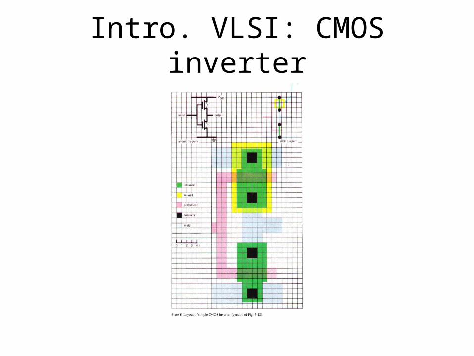
Intro. VLSI: CMOS inverter
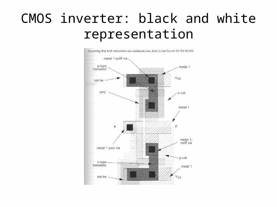
CMOS inverter: black and white representation
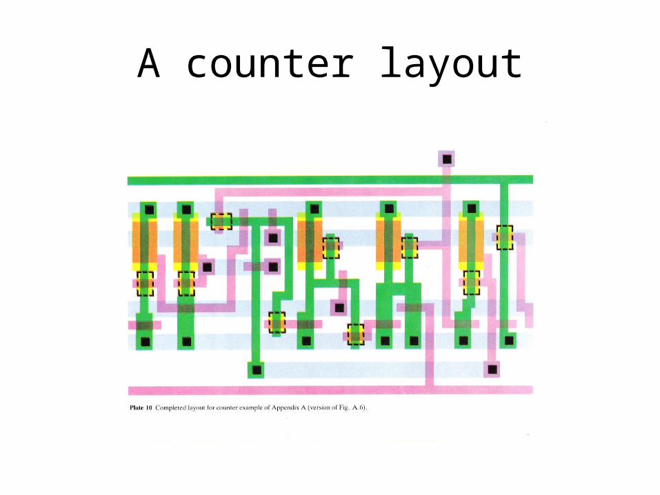
A counter layout
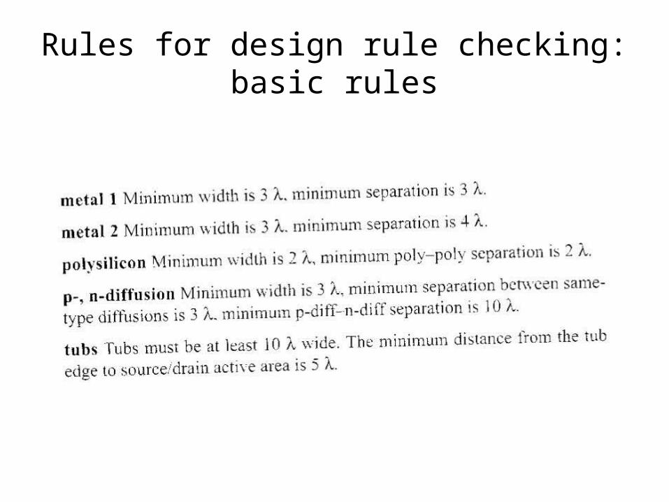
Rules for design rule checking:basic rules
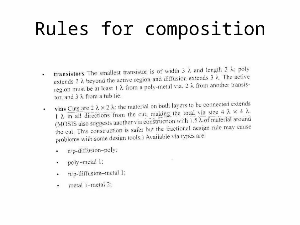
Rules for composition
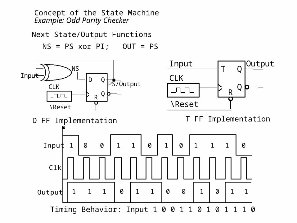
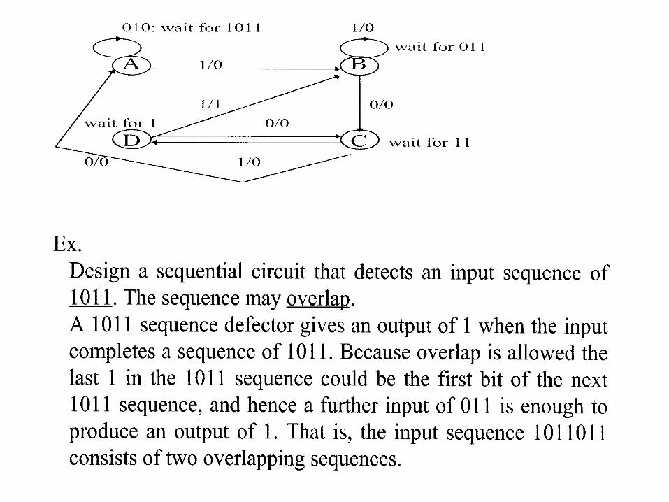
Concept of the State MachineExample: Odd Parity Checker
Next State/Output Functions
NS = PS xor PI; OUT = PS
D
R
Q
Q
Input
CLK PS/Output
\Reset
NS
D FF Implementation
T
R
Q
Q
Input
CLK
Output
\Reset
T FF Implementation
Timing Behavior: Input 1 0 0 1 1 0 1 0 1 1 1 0
Clk
Output
Input 1 0 0 1 1 0 1 0 1 1 1 0
1 1 0 1 0 0 1 1 0 1 1 1
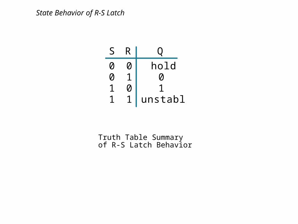
State Behavior of R-S Latch
Truth Table Summary of R-S Latch Behavior
Q
hold 0 1
unstable
S
0 0 1 1
R
0 1 0 1
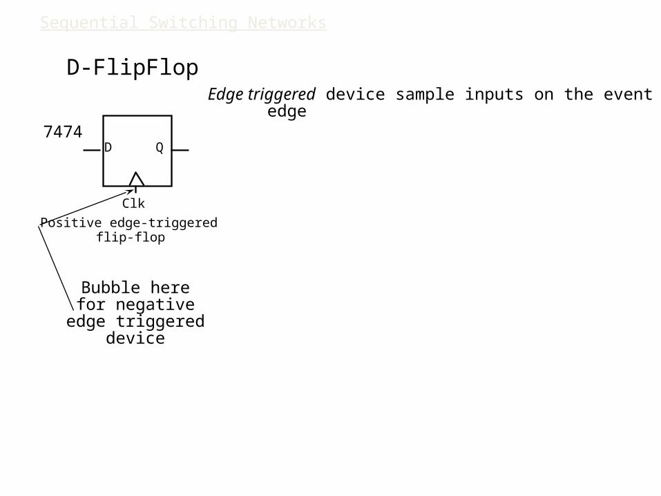
Sequential Switching Networks
Edge triggered device sample inputs on the event edge
7474
Bubble herefor negative
edge triggereddevice
Positive edge-triggered flip-flop
D Q
Clk
D-FlipFlop
In
Q 0
Q 1
Clk
100
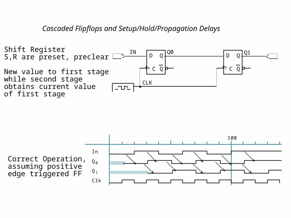
Cascaded Flipflops and Setup/Hold/Propagation Delays
Shift RegisterS,R are preset, preclear
New value to first stagewhile second stageobtains current valueof first stage
Correct Operation,assuming positiveedge triggered FF
IN
CLK
Q0 Q1D
C
Q
Q
D
C
Q
Q
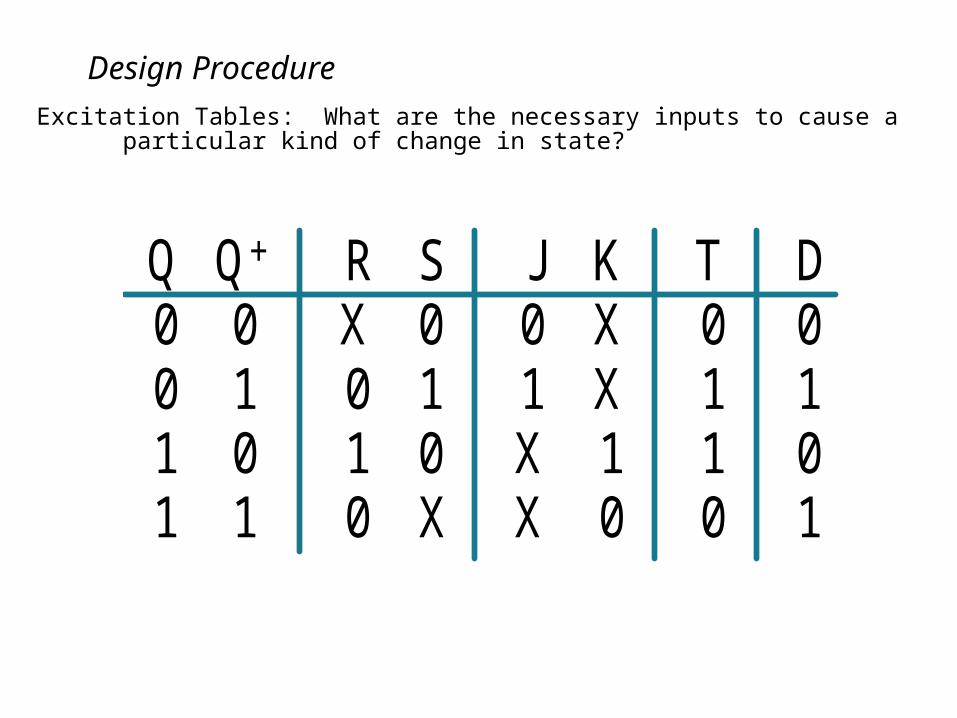
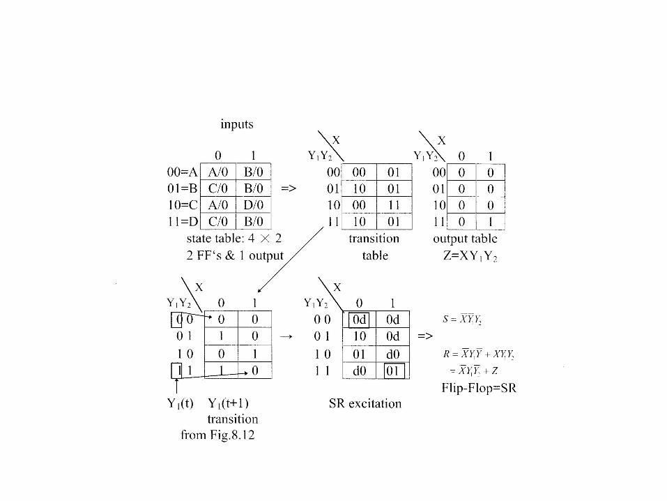
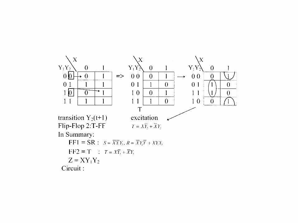
Design ProcedureExcitation Tables: What are the necessary inputs to cause a particular kind of change in state?
D 0 1 0 1
T 0 1 1 0
Q + 0 1 0 1
Q 0 0 1 1
S 0 1 0 X
R X 0 1 0
K X X 1 0
J 0 1 X X