54
ECE 3551 Microcomputer Systems 1 EVM OMAP L137 DSP 6747 + ARM9

ECE 3551 Microcomputer Systems 1
EVM OMAP L137DSP 6747 + ARM9

May 7, 2023 Veton Këpuska 2
Highlights Dual Core
375/456-MHz ARM926EJ-S™ RISC MPU 375/456-MHz C674x VLIW DSP
TMS320C674x Fixed/Floating-Point VLIW DSP Core
Enhanced Direct-Memory-Access Controller 3 (EDMA3)
128K-Byte RAM Shared Memory Two External Memory Interfaces Three Configurable 16550 type UART Modules LCD Controller
May 7, 2023 Veton Këpuska 3
Highlights Two Serial Peripheral Interfaces (SPI) Multimedia Card (MMC)/Secure Digital (SD) Two Master/Slave Inter-Integrated Circuit One Host-Port Interface (HPI) USB 1.1 OHCI (Host) With Integrated PHY
(USB1)
May 7, 2023 Veton Këpuska 4
Outline
•Features1•Board Components2•Board Layout3

May 7, 2023 Veton Këpuska 5
Features
•Features1•Board Components2•Board Layout3

May 7, 2023 Veton Këpuska 6
Features A Texas Instruments OMAP-L137 device with a C674x
VLIW DSP floating point processor and an ARM926EJ-S processor operating up to 300 Mhz.
64 Megabytes SDRAM SPI Boot EEPROM 2 Port Ethernet Phy/switch SD/MMC/MMC Plus media card interfaces TLV320AIC3106 Stereo Codec USB 1.1 High speed interface USB2 2.0 Full speed interface RS-232 Interface

May 7, 2023 Veton Këpuska 7
Features On chip real time clock Configurable boot load options 4 user LEDs/4 position user DIP switch Single voltage power supply (+5V) Expansion connectors for daughter card use Embedded JTAG Emulation 14 Pin TI JTAG/20 Pin ARM JTAG Interfaces

May 7, 2023 Veton Këpuska 8
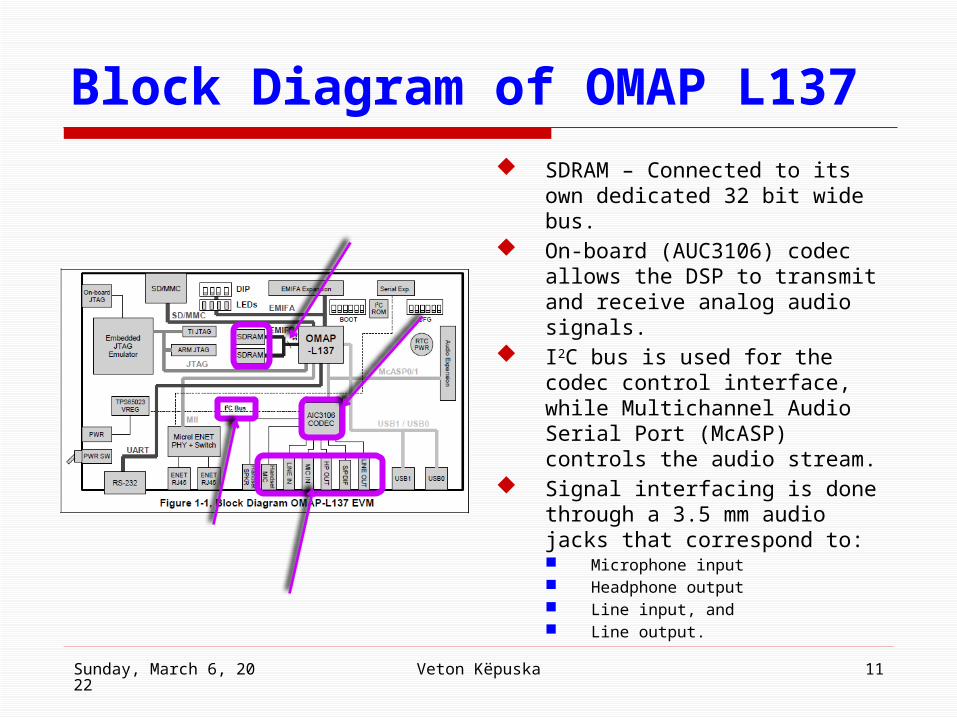
Block Diagram of OMAP L137

May 7, 2023 Veton Këpuska 9
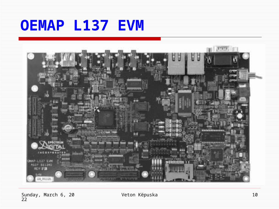
OEMAP L137 EVM
May 7, 2023 Veton Këpuska 10
OEMAP L137 EVM
May 7, 2023 Veton Këpuska 11
Block Diagram of OMAP L137
SDRAM – Connected to its own dedicated 32 bit wide bus.
On-board (AUC3106) codec allows the DSP to transmit and receive analog audio signals.
I2C bus is used for the codec control interface, while Multichannel Audio Serial Port (McASP) controls the audio stream.
Signal interfacing is done through a 3.5 mm audio jacks that correspond to: Microphone input Headphone output Line input, and Line output.

May 7, 2023 Veton Këpuska 12
Block Diagram of OMAP L137
4 user LEDs 4 position DIP switch On-chip real time clock. On board multiplexing allows
interfacing with the daughter cards.
+5 V external power supply is used to power the board. On-board switching voltage
regulators provide the CPU core voltage for peripheral interfacing: +3.3V +1.8V
The boards is held in reset by the on boards power controller until these supplies are within operating specifications.
Code Composer Studio/Eclipse communicates with the EVM through an embedded emulator or via the TI 14 pin or ARM 20 pin external JTAG connectors.

May 7, 2023 Veton Këpuska 13
Basic Operation The EVM is designed to work with:
TI’s Code Composer Studio IDETM, or MontaVista tool environments.
Code Composer/Eclipse communicates with the board through an on board JTAG emulator.

May 7, 2023 Veton Këpuska 14
Boot Switch Settings The EVM has a 5 position
switch that allow users to configure the operational state of the processor when it is released from reset and determine the source for processor booting.
May 7, 2023 Veton Këpuska 15
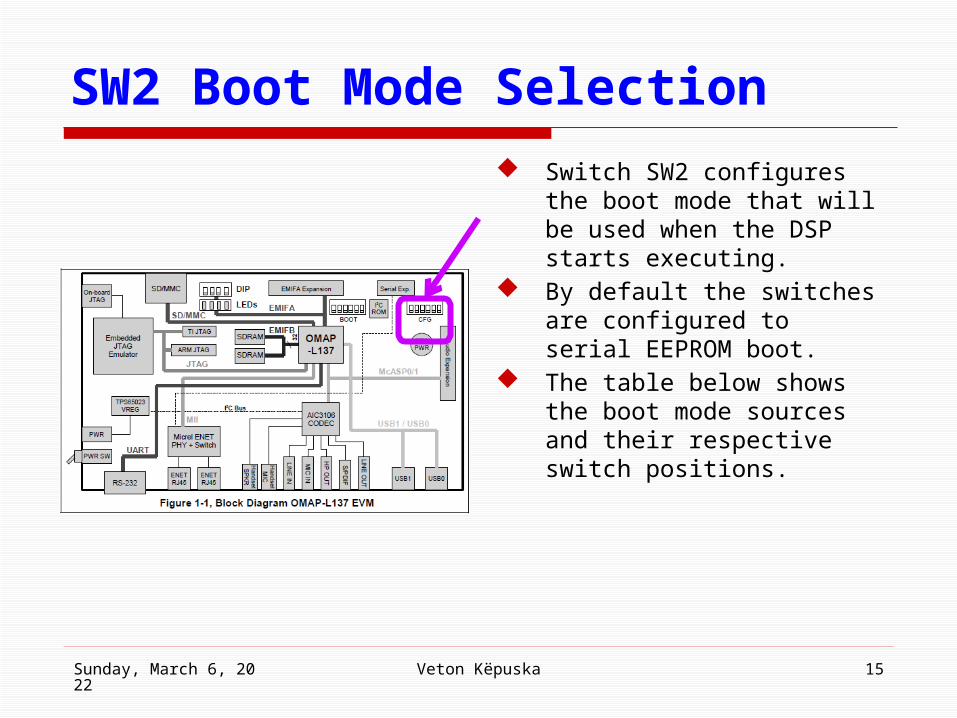
SW2 Boot Mode Selection Switch SW2 configures the
boot mode that will be used when the DSP starts executing.
By default the switches are configured to serial EEPROM boot.
The table below shows the boot mode sources and their respective switch positions.

May 7, 2023 Veton Këpuska 16
SW2 Boot Mode Selection

May 7, 2023 Veton Këpuska 17
Board Components
• Features1• Board Components2• Board Layout3

May 7, 2023 Veton Këpuska 18
Board Components Outline• EMIF-A Interfaces1• EMIF-B SDRAM Memory Interface2• Memory Card Interface3• UART Interface4• USB Interface5• AIC3 106 Interface6• Ethernet Interface7• Daughter Card Interface8

May 7, 2023 Veton Këpuska 19
External Memory InterfaceEMIF-A Interfaces A separate 16 bit EMIF with three chip enables
divide up the address space and allow for asynchronous accesses on the EVM.
The EVM uses this interface for peripheral interfaces to the daughter card.

May 7, 2023 Veton Këpuska 20
EMIF-B SDRAM Memory Interface The OMAP-L137 device incorporates a
dedicated 32 bit wide SDRAM memory bus. The EVM uses two 256 Megabit, 16 bit wide
memories on this bus, for a total of 64 megabytes of memory for program, data, and video storage.
The internal SDRAM controller uses a PLL to control the SDRAM memory timing. Memory refresh for SDRAM is handled automatically by the OMAP-L137 internal SDRAM controller.
May 7, 2023 Veton Këpuska 21
Memory Card Interface The EVM supports SD/MMC/MMC PLUS media
card interfaces. This interface is multiplexed with other function
the EMIFA bus.

May 7, 2023 Veton Këpuska 22
UART Interface The internal UART2 on the OMAP-L137 device is
driven to connector P1. The UART’s interface is routed to the RS-232
line drivers prior to being brought out to a DB-9 connector, P1.

May 7, 2023 Veton Këpuska 23
USB Interface The OMAP-L137 incorporates two on chip USB
controllers. The USB 2.0 interface is brought out to a micro
A/B connector. A jumper is provided to make a flexible host, peripheral, and USB on the go interface.
The second USB 1.1 interface is brought out to an A type host interface connector.
May 7, 2023 Veton Këpuska 24
AIC3106 Interface The EVM incorporates a Texas Instruments
TLV320AIC3106 stereo codec for input and output of audio signals.
The codec samples analog signals on the microphone or line inputs and converts them into digital data so it can be processed by the DSP.
When the DSP is finished with the data it uses the codec to convert the samples back into analog signals on the line output so the user can hear the output.

May 7, 2023 Veton Këpuska 25
AIC3106 Interface The codec communicates using two serial
channels, one to control the codec’s internal
configuration registers and one to send and receive digital audio
samples. The I2C bus is used as the AIC3106’s control
channel. The control channel is generally only used when configuring the codec, it is typically idle when audio data is being transmitted.

May 7, 2023 Veton Këpuska 26
AIC3106 Interface McASP1 is used as the bi-directional data
channel. All audio data flows through the data channel.
Many data formats are supported based on the three variables of: 1) sample width, 2) clock signal source and 3) serial data format.
The EVM examples generally use a 16-bit sample width with the codec in master mode so it generates the frame sync and bit clocks at the correct sample rate without effort on the DSP side.

May 7, 2023 Veton Këpuska 27
AIC3106 Interface The codec is clocked via a 24.576 Mhz
oscillator. The internal sample rate generator subdivides
the default system clock to generate common audio frequencies.
The sample rate is set by a codec register.

May 7, 2023 Veton Këpuska 28
OMAL-L137 Codec Interface

May 7, 2023 Veton Këpuska 29
Ethernet Interface The OMAP-L137 incorporates an Ethernet MAC
which interfaces to a (Microtel KSZ8893MQL) Ethernet switch.
The multi-port 10/100 Mbit interface is isolated and brought out to two RJ-45 standard Ethernet connectors: P9, P10.
The Ethernet addresses is stored in the on board I2C EEPROM.
The 2 Ethernet addresses stored in the EEPROM are the first address and the second address + 1. The first address should always be an even number.

May 7, 2023 Veton Këpuska 30
Ethernet Interface The I2C bus is also used to control
configuration registers in the switch. Two ports provide the ability to input and pass
data for Voice Over IP (VOIP) or other daisy chained applications.
Connector P9 is the primary port for normal operation.
The RJ-45 jacks have 2 LEDs integrated into their connector.
The LEDs are green and yellow and provide link and transmit status from the Ethernet controller.

May 7, 2023 Veton Këpuska 31
Ethernet Interface The MAC address for each EVM is also written
on a label on the bottom of the board. The figure below shows an examples of this.
May 7, 2023 Veton Këpuska 32
I2C0 Interface The I2C0 bus on the OMAP-L137 is ideal for
interfacing to the control registers of many devices.
On the OMAP-L137 EVM the I2C0 bus is used to configure the Ethernet and Codec. An I2C ROM is also interfaced via the serial bus.

May 7, 2023 Veton Këpuska 33
Daughter Cart Interfaces The EVM provides expansion connectors that
can be used to accept plug-in daughter cards. The daughter card allows users to build on their
EVM platform to extend its capabilities and provide customer and application specific I/O.
The EMIF-A signals are brought out as LCD, peripheral, or EMIF signals.

May 7, 2023 Veton Këpuska 34
Outline
• Features1• Board Components2• Board Layout3
May 7, 2023 Veton Këpuska 35
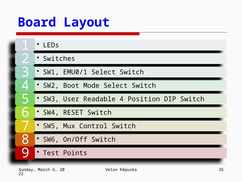
Board Layout• LEDs1• Switches2• SW1, EMU0/1 Select Switch3• SW2, Boot Mode Select Switch4• SW3, User Readable 4 Position DIP Switch5• SW4, RESET Switch6• SW5, Mux Control Switch7• SW6, On/Off Switch8• Test Points9

May 7, 2023 Veton Këpuska 36
Board Layout

May 7, 2023 Veton Këpuska 37
Connectors

May 7, 2023 Veton Këpuska 38
LEDs The EVM has ten (10) LEDs which are located
on the top side of the board. Information regarding the LEDs are shown in
the table.

May 7, 2023 Veton Këpuska 39
Switches The EVM has six (6) switches. The function of these switches are shown in the
table.

May 7, 2023 Veton Këpuska 40
SW1, EMU0/1 Select Switch SW1 is a 2 position DIP switch providing 4
options in selecting the state of the EMU0 and EMU1 pins on the OMAP-L137 processor.
This switch is not needed for the OMAP-L137 processor.
The default is to select pull ups on the EMU0 and EMU1.

May 7, 2023 Veton Këpuska 41
SW2, Boot Mode Select Switch
Switch SW2 is a 6 position DIP switch. Only 5 of the positions are used. Note that only 5 combinations provide valid options.
The boot mode options are described in the table.

May 7, 2023 Veton Këpuska 42
SW2, Boot Mode Select Switch The table below shows the position settings
which select the various boot modes.

May 7, 2023 Veton Këpuska 43
SW3, User Readable 4 Position DIP Switch
Switch SW3 is a 4 position DIP switch mapped to EMIFA data bus lines D8-D11 via a multiplexer.
The table shows what signal each position appears on.
May 7, 2023 Veton Këpuska 44
SW4, RESET Switch Switch SW4 is a push button reset switch that
will RESET the board.

May 7, 2023 Veton Këpuska 45
SW5, Mux Control Switch Switch SW5 is a 6
position DIP switch. This switch allows enabling on mux control signals. The six signals that can be pulled up are shown in the table.
Alternatively the multiplexer control lines can be enabled via daughter card connectors. Additional control lines are mapped to the daughter card connectors.

May 7, 2023 Veton Këpuska 46
SW6, On/Off Switch Switch SW6 is an on/off toggle switch that
allows +5 volts from the J6 connector to be applied to the board.
May 7, 2023 Veton Këpuska 47
Test Points The EVM has 49 test points. All test points
appear on the top of the board. The following figure identifies the position of
each test point. The next table lists each test point and the
signal appearing on that test point.

May 7, 2023 Veton Këpuska 48
Test Points

May 7, 2023 Veton Këpuska 49
OMAP-L137 EVM Test Points
May 7, 2023 Veton Këpuska 50
Power Test Points There are 10 power test point pairs for major
power domains on the EVM. These test points provide a convenient
mechanism to check the EVM’s multiple power supplies.
The table below shows the voltages for each test point and what the supply is used for.

May 7, 2023 Veton Këpuska 51
Power Test Points

May 7, 2023 Veton Këpuska 52
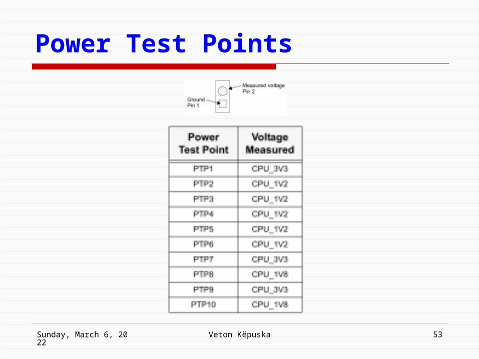
Power Test Points Furthermore the EVM has ten 2 pin power test
points for specific power domains on the L137 device.
These voltages are measured across a resistor which is why there are two points to each test position. The square pad is the ground. The round pad is the measured voltage.
The figure below shows what a typical power test point looks like.
May 7, 2023 Veton Këpuska 53
Power Test Points

May 7, 2023 Veton Këpuska 54
END


