MEASUREMENT 2011, Proceedings of the 8th International Conference, Smolenice, Slovakia 95 Dimensional Micro- and Nanometrology at PTB R. Köning, J. Flügge, D. Hüser, W. Haessler-Grohne, H.U. Danzebrink, G. Dai, U. Brand, V. Nesterov, S. Bütefisch, G. Ehret, M. Wurm, B. Bodermann, E. Buhr, H. Bosse Physikalisch-Technische Bundesanstalt (PTB), Bundesallee 100,38116 Braunschweig, Email: [email protected]Abstract. In this contribution we will provide an overview of the current state and the actually ongoing developments in the field of dimensional micro- and nanometrology at PTB. That is, we will report on the methods and instruments developed, applied and that are in development for high precision, traceable measurements in these important areas of dimensional metrology. Keywords: Dimensional Metrology, Nanometrology, Micrometrology, Traceability 1. Introduction The control of the geometrical dimensions in the industrial production of single components and whole systems demands appropriate measurement techniques. The related measurement instruments have to be chosen according to different criteria like throughput, robustness, price, 3D-capability, in-line ability, measurement range, required resolution and accuracy. Meanwhile, dimensional features in the area of micro- and microsystem technology can be characterized and controlled during production on the basis of traceable measurement results in the same way as in conventional manufacturing process control. In nanotechnology the desired properties of the product often depend much stronger on the geometrical dimensions or even appear as a consequence of the reduced dimensions and therefore even tighter specifications have to be met. Here the progress made in the available measurement equipment over the last two decades has just enabled this field of technology. Dimensional metrology instruments aiming at the smallest measurement uncertainties achievable have to comply with two fundamental requirements. Firstly a well-designed and well-characterized positioning system, which provides a relative movement of the measurement object with its functional dimensional features of interest with respect to the probing system of the measurement instrument, is mandatory. Secondly, a sound physical model of the interaction of the probing system with the dimensional features of the sample should be available and applied in the evaluation of the measurement results. This is particularly important if the size of the features comes close to the resolution limit of the probing system. The measurement of some geometrical properties, for example the diameter of nanoparticles, is simply impossible without considering the probe sample interaction. We will show examples of different probing methods in this paper, namely tactile, opto- tactile, optical and electron beam methods and discuss challenges for future developments in micro- and nanometrology. 2. Micrometrology In micrometrology the dimensions of measurement objects are usually in the range of some 100 m to some mm. Typically the required measurement uncertainties of the dimensional features are in the range of 0.1 μm or below. Several metrology institutes developed, built and meanwhile operate suitable reference measurement systems for dimensional characterization
Transcript
MEASUREMENT 2011, Proceedings of the 8th International Conference, Smolenice, Slovakia
95
Dimensional Micro- and Nanometrology at PTB
R. Köning, J. Flügge, D. Hüser, W. Haessler-Grohne, H.U. Danzebrink, G. Dai, U. Brand, V. Nesterov, S. Bütefisch, G. Ehret, M. Wurm, B. Bodermann, E.
Abstract. In this contribution we will provide an overview of the current state and the actually ongoing developments in the field of dimensional micro- and nanometrology at PTB. That is, we will report on the methods and instruments developed, applied and that are in development for high precision, traceable measurements in these important areas of dimensional metrology.
The control of the geometrical dimensions in the industrial production of single components and whole systems demands appropriate measurement techniques. The related measurement instruments have to be chosen according to different criteria like throughput, robustness, price, 3D-capability, in-line ability, measurement range, required resolution and accuracy. Meanwhile, dimensional features in the area of micro- and microsystem technology can be characterized and controlled during production on the basis of traceable measurement results in the same way as in conventional manufacturing process control. In nanotechnology the desired properties of the product often depend much stronger on the geometrical dimensions or even appear as a consequence of the reduced dimensions and therefore even tighter specifications have to be met. Here the progress made in the available measurement equipment over the last two decades has just enabled this field of technology.
Dimensional metrology instruments aiming at the smallest measurement uncertainties achievable have to comply with two fundamental requirements. Firstly a well-designed and well-characterized positioning system, which provides a relative movement of the measurement object with its functional dimensional features of interest with respect to the probing system of the measurement instrument, is mandatory. Secondly, a sound physical model of the interaction of the probing system with the dimensional features of the sample should be available and applied in the evaluation of the measurement results. This is particularly important if the size of the features comes close to the resolution limit of the probing system. The measurement of some geometrical properties, for example the diameter of nanoparticles, is simply impossible without considering the probe sample interaction.
We will show examples of different probing methods in this paper, namely tactile, opto-tactile, optical and electron beam methods and discuss challenges for future developments in micro- and nanometrology.
2. Micrometrology
In micrometrology the dimensions of measurement objects are usually in the range of some 100 m to some mm. Typically the required measurement uncertainties of the dimensional features are in the range of 0.1 µm or below. Several metrology institutes developed, built and meanwhile operate suitable reference measurement systems for dimensional characterization
MEASUREMENT 2011, Proceedings of the 8th International Conference, Smolenice, Slovakia
96
of microcomponents and microsystems [1-3]. Optimized probe systems adapted to these small objects, which were required have been developed as well. Here the reduction and a better control of the probing force had to be established. The contributions of the PTB also were threefold, namely development of a reference micro-CMM [1], the development of improved probing systems [4-8] and the development of a micro- and nanoforce measurement facility [9,10].
Micro- and Nanoforce facility
Fig. 1. Schematic of the Micro- and Nanoforce measurement facility (left) and the measured force caused by an
incident laser beam
The necessary reduction of the probe size and the probing force required to measure the dimensions of microstructures sufficiently accurate possessed a real challenge. In order to be able to measure these forces as well as the stiffness of AFM cantilevers a Micro- and Nanonewton measurement facility has been built [9,10], which has a measurement range from 10 µN to 1 nN with a resolution of 1 pN. It is based on the measurement of the displacement of a disc pendulum and uses electrostatic stiffness reduction and force compensation. In addition an identical reference pendulum is employed for the compensation of thermal and seismic noise. It is shown in Fig. 1 together with the measurement results of the force acting in case a laser beam ( = 633nm) with an optical power of 7 mW hits the measurement disc.
Microprobe developments Historically an opto-tactile probe was first developed and also transferred to industry as a 2D measurement probe [4]. It basically consists of a fiber ball probe with diameters down to 15 µm which is illuminated by the fibre and whose position is measured with a CCD camera. This system recently was enhanced to provide full 3D probing capability by analysis of the speckle pattern of a fibre ball if it is illuminated by a coherent light source [5].
In addition a 3D tactile microprobe was developed in cooperation with the Institute for Microtechnology at the TU Braunschweig. Here the deformation of a so-called silicon boss membrane is measured by means of integrated piezoresistive transducers [6]. The deformation of the membrane is caused by deflections of a microprobe fixed to the centre part of the membrane (boss). This 3D sensor allows to measure forces as well as displacements and different probe configurations were reported (ball diameter, shaft length, boss type). Both types of probe are used in the CMM (see below). A third development of a probe system which is also suitable for characterization of microcomponents is an assembled cantilever probe (ACP) [7]. Here two AFM-cantilevers are glued together so that they form approxi-
MEASUREMENT 2011, Proceedings of the 8th International Conference, Smolenice, Slovakia
97
Fig 2. Microprobe systems developed and used at the PTB for characterization of microcomponents. Left: opto-tactile 3D probe; middle: Si boss membrane 3D microprobe (with Euro Cent coin for size comparison); right: ACP probe (assembled cantilever probe).
mately a right angle (see fig. 2), so that the deflection of the 1st, vertical cantilever can be transferred to the 2nd, horizontal cantilever and detected by a conventional AFM head. The ACP probes have been used successfully to measure the form of sidewalls of micro gears [7]. Fig. 2 shows the three described microprobe systems, which all allow to measure the dimensional features of interest on the accessible surface areas of microcomponents.
For the characterization of object features which are normally inaccessible for tactile probes or which are completely hidden within the measurement object, like e.g. inclusions, x-ray based industrial computed tomography (CT) techniques are increasingly used. The PTB has contributed to this metrology area by development of suitable standards and by basic investigations with respect to the traceability of the CT measurement results [11] and will continue to investigate the application of CT techniques also in the field of micrometrology.
Reference Micro Coordinate Measuring Machine
Fig. 3. Schematic of the µCMM (left) and typical repeatability of a flatness measurement (md: distance of the measurement trace the of fibre probe from the upper edge of the optical flat)
The CMM is based on a commercially available coordinate measuring machine with improved air bearings and high resolution Zerodur scales using an opto-tactile fibre probe for the localization of microstructures. It has been equipped with a metrology frame, which contains six laser interferometers for high-precision position and guiding deviation measurements, a Zerodur cuboid carrying the mirror surfaces for the laser interferometers to which the fibre probe is fixed, and an invar support for the measuring objects to which the reference mirrors of the interferometers are fixed. This led to a reduced measurement volume of 24 mm x 34 mm x 35 mm. The orthogonality and flatness deviations of the Zerodur measuring surfaces have been measured and taken into account in the equation of motion of
MEASUREMENT 2011, Proceedings of the 8th International Conference, Smolenice, Slovakia
98
the probing sphere. Therefore the CMM is capable of providing directly traceable measurements. As a first performance test, the flatness of an optical flat has been measured with the fibre probe. Measuring-depth-dependent and probing-force-dependent shifts of the probing position were observed. In order to reduce the scattering of the probing points, 77 data sets were taken and averaged for the measurement of one coordinate point. This has led to measuring times of several hours for one plane and to strong thermal drifts. A typical repeatability of this type of measurements is shown in the diagram of figure 3. The expanded measurement uncertainty is 236 nm. If the drift contribution is omitted 61 nm are obtained so that the uncertainty can be considerably reduced by a reduction of the measurement time.
In addition a F25, a µCMM made by Zeiss was investigated. It offers a much larger range of 130 mm x 130 mm x 100 mm, which also leads to an increase of the achievable measurement uncertainty. It closes the gap in the measurement capabilities of the large CMMs and the CMMs. Zeiss specifies an uncertainty of about (0.4 +L/666) m, where L is in mm. Recent investigations at PTB on calibration objects like a special Zerodur ball plate have shown, that measurement uncertainties in the range of 50 nm for the ball positions could be achieved under optimum circumstances with this type of µCMM.
The transition from micro- to nanometrology is smooth. There are objects with outer dimensions in the mm range with either nanosized features of interest or with very small dimensional tolerances, which need to be characterized precisely. In order to deal with this challenge, a metrological large range scanning probe microscope (LR-SPM) was developed at the PTB [12] which allows to use the full positioning range of 25 mm x 25 mm x 5 mm of the so-called Nano Positioning and Nano Measuring Machine [12] for traceable dimensional measurements with a nominal resolution of 0.1 nm. The motion control, data acquisition and data evaluation software of this instrument has recently been enhanced by integration of the CMM software Quindos. Therefore it can now be applied to precisely calibrate 3D reference objects for micro-coordinate metrology. Figure 3 shows on the left side a set of two spheres in a nominal distance of 3 mm with 1 mm radius each and an example of the repeatability of distance calibrations, which was obtained by the LR-SPM using the Si boss membrane probe shown before [6]. Also shown in the same figure on the right side is an SEM image of a precision micropyramid with landmark type test structures, which was produced by focussed ion beam figuring techniques. Such a micropyramid structure can be calibrated by instruments like e.g. the metrological LR-SPM and can then be used as a 3D calibration artefact for other types of SPMs or SEMs [13].
MEASUREMENT 2011, Proceedings of the 8th International Conference, Smolenice, Slovakia
99
Fig. 4. Left: Test object of 2 small spheres in 3 mm nominal distance with 1 mm radius each and repeatability of the distance measurement results as obtained by the metrological LR-SPM of the PTB. Right: SEM (top) and SPM image (34 µm scan range) of a micropyramid which is used as a 3D microscope calibration artefact.
Nanometrology
Nanotechnology usually utilizes size-dependent phenomena that enable novel applications [14], which usually start to appear at feature sizes smaller than 100 nm. It requires the understanding and control of matter and processes at the nanoscale, below 100 nanometres in one or more dimensions. In order to be able to control the related processes, appropriate measurement techniques with an adequate spatial resolution have to be developed and employed. Here we will provide an overview of the measurement capabilities of the PTB in dimensional nanometrology.
As already mentioned in the preceding section there are also microstructures whose dimensional properties, like height, width and distance, have to be measured with uncertainties in the nanometer range. Probably the highest requirements occur in surface metrology. Here the “high resolution topo scan” (HRTS) [15], a 2-dimensional surface profiler, developed at the PTB, started to operate lately. For one-dimensional traceable length calibrations of line scales, photomasks and incremental encoders on substrates up to 600 mm with uncertainties down to a few nm only, the PTB is operating a special vacuum interference comparator, the so-called “Nanometer Comparator” [16,17]. The length of gauge blocks with suitable surface quality can be measured with even lower uncertainty [18]. Such samples are used to determine the thermal expansion coefficients and the compressibility and to investigate the stability of materials. The accurate knowledge of these material parameters, including their uncertainties, is a necessary prerequisite for measurements of larger parts with measurement uncertainties in the single nanometer range. Small angle measuring devices are key components in deflectometer set-ups which are used for high precision flatness and synchrotron mirror metrology [19]. They have also to be used for the characterization of the angle deviation of the scan apparatus, which are required for a reliable determination of the Abbe error contribution to the measurement uncertainty. Such measurements require high precision angle calibrations. Therefore investigations are ongoing to improve the measurement performance of electronic autocollimators and their calibration procedures [20].
Optical methods Optical microscopy is despite its rather low resolution still widely in use in nanotechnology. Progress in the technology of available light sources, in the design of optical materials, elements and their production, the efficiency of the image detectors (CCD-cameras as well as photo diodes and photomultipliers) lead together with the increase of the image data acquisition and processing capabilities to a steady increase of their performance. The PTB already participates in these developments for a long time. High resolution optical UV microscopes operating at a wavelength of 365 nm are already in use for quite a while in the line width and photo mask calibration service.
Fig. 5 shows a schematic of the new deep UV transmission microscope [21], which is currently being set up and which is especially designed for line width (critical dimensions or CD) measurements of micro- and nanostructures. The optical resolution is about 100 nm. The main application will be CD metrology of photo masks used in optical lithography. The high lateral resolution will be obtained by using of 193 nm excimer laser radiation for illumination
in conjunction with a high-aperture objective (NA= 0.9) of highest quality (Strehl ratio 0.99)
MEASUREMENT 2011, Proceedings of the 8th International Conference, Smolenice, Slovakia
100
Fig. 5. Schematic of the new 193 nm microscope and first performance data
The illumination and imaging system will provide various imaging modes, ranging from ordinary brightfield to specially structured illumination schemes. Traceability will be accomplished through an integrated laser interferometer. The mechanical set-up is characterized by an ultra-stable bridge construction on a granite base and has been designed with special emphasis on realizing a positioning stability in the nanometer range. The projected (2) measurement uncertainty for line width measurements on photomasks (chromium on quartz) is only 10 nm.
Another trend is the use of non-imaging methods for the measurements of nanostructures. Figure 6 shows the basic operation principle and the realization of the new DUV scatterometer of the PTB [22]. This versatile setup allows reflectrometric, diffractometric and ellipsometric measurements of a wide range of different samples and various wavelengths ranging from 840 nm down to 193 nm.
Fig. 6. Basic operation principle and realization of the new PTB DUV scatterometer.
The optical diffraction pattern of grating structures does not only contain information about the mean pitch, but also about other dimensional features of interest of the grating structures like the height, top CD or bottom CD and sidewall angle. To extract information on these structure parameters from measured optical diffraction pattern, one has to solve the inverse scattering problem. Therefore it is necessary to rigorously model the interaction of light with a 3D structure geometry, for which PTB uses Maxwell solvers either based on the rigorous coupled wave analysis method (RCWA) or a finite element method (FEM) [23]. Such simulations are also required for the aforementioned line width measurements by means of optical microscopy. Due to the mathematical complexity of this particular task, the PTB closely cooperates with institutes of applied mathematics [24].
The wavelength used at the PTB scatterometers for the characterization of nanograting structures ranges from the VIS over DUV (193 nm) to EUV (13 nm). The latter wavelength range is available at the Berlin synchrotron storage rings BESSY II and the new PTB Metrology Light Source (MLS) [25].
MEASUREMENT 2011, Proceedings of the 8th International Conference, Smolenice, Slovakia
101
In the recent international comparison on 2D gratings called Nano 5 [26], the PTB has participated with a diffractometer (=496 nm, 476 nm and 266 nm) set-up and with the LR-SPM. The measurement results of both instruments on the two comparison standards with nominal pitches of 300 nm and 1000 nm were in good agreement with the comparison reference values. Standard uncertainties of the PTB results e.g. for the mean x-pitch of the 300 nm 2D grating sample were 12 pm for the diffractometer and 5.6 pm for the LR-SPM. In contrary to the diffraction methods the LR-SPM also provides information on the local pitch variation of the sample. Another international comparison on optical diffraction measurements of 1D gratings also showed a good agreement of results between the four participating national metrology institutes [27].
Scanning electron microscopy In the preceding section the importance of appropriate physical models for the simulation of the measurement signal and for the extraction of the measurand out of this signal was emphasized. These are necessary prerequisites for traceable measurements as well as for the accurate determination of the accompanying measurement uncertainties of these precision measurements. In electron beam based metrology, especially in scanning electron microscopy (SEM) the situation is similar, although the primary SEM beam spot offers a much higher resolution of down to 1 nm only. However, the primary electrons initiate a series of elastic and inelastic scattering events in the solid state material which effectively reduce the achievable spatial resolution. For the simulation of these scattering events and for the generation of secondary and backscattered electrons which are detected for SEM image signal generation, the PTB uses its self-developed Monte Carlo based simulation programs [28].
EOMS iso opaque, top CD UV iso opaque: CD @ 50% height
400 nm
1000 nm160 nm
Expected Differencefor h = 74 nm, 84°:CD@ 50% - top CD = 8 nm
8 nm
U95%
U95%
Fig. 7. The Electron Optical Metrology System in the PTB clean room centre and results of CD calibrations by the EOMS (top CD) and UV transmission microscopy (CD at 50 % height of the line features [29]).
On the basis of these simulation programs, the PTB has developed special edge detection algorithms, which are used for traceable SEM line width metrology. One example is an exponential fit operator for determination of the top width of a line which is based on the electron diffusion characteristics of secondary electrons emitted in the vicinity of edges of line structures. Figure 7 shows a photo of the Electron Optical Metrology System (EOMS) which is used for SEM measurements on larger planar objects together with the results of a comparison measurement with UV transmission microscopy on different line features on a chrome on quartz mask [29]. Another application of SEM modeling and measurement of increasing importance, that has been pursued by the PTB, is the traceable characterization of the size and shape of nanoparticles [30]. Here the PTB also collaborates with partners from academia, other national metrology institutes and industry in an EU-funded project.
MEASUREMENT 2011, Proceedings of the 8th International Conference, Smolenice, Slovakia
102
Scanning Probe Microscopy Scanning probe microscopy (SPM) has also an important role in high resolution characterization as well as in the creation and manipulation of nanostructures and nanoobjects. The PTB is involved in the field of scanning probe based dimensional metrology since it emerged.
The first metrology instruments were home-built scanning tunnelling microscopes (STMs) with a capacitive based position feedback employed to overcome the insufficient properties of the piezoelectric materials used to provide the scan motion. The capacitive displacement sensors were calibrated by means of heterodyne interferometry [31,32]. Both, a scanning sample design as well as a scanning probe design were implemented. However, STM measurements can only be performed at well conducting samples and, due to the very small tip sample distance, with very low speed. Therefore the scanning force detection scheme was adapted as soon as it became available [33]. The use of scanning optical near field microscopes was also investigated [34]. Due to the difficulties in the interpretation of the images and the lack of high quality commercially available probes these activities were abandoned. The plans to obtain well defined position standards by producing nanostructures coupled to the surface lattice using SPM based nanolithography were also dismissed due to missing knowledge of the fundamentals of the structure formation process [35]. Also an ultra-precision interference comparator that used two scanning tunnelling microscopes as surface probes [36] was implemented. The instrument was supposed to measure gauge blocks but the measurement uncertainties achieved were far behind those of the optical gauge block interferometers [18] and therefore this approach was not followed further. In addition, in a collaboration with the TU Ilmenau, interferometers where integrated in the AFM Veritekt (built by former company Carl Zeiss Jena) to set up a traceable metrology AFM [37]. Other instrument developments were the successful adaptation and upgrade of the Nano Measuring Machine NMM (from SIOS Messtechnik GmbH) to the metrological LR-SPM already mentioned, the development of a large sample AFM (Nanostation 300, development performed in cooperation with former company S.I.S.) for measuring photomasks [38], the integration of home built STM and AFM with the combined optical and X-ray interferometer (COXI) [39,40] and the AFM designed to study tip-sample interactions [41]. In addition a number of commercial instruments are in use. Currently an AFM with a short scan range (5 m x 5 m x 5 m) is being set up. It comprises of a novel type of CMOS sensor based and FPGA processed interferometers. This AFM is intended for highly accurate measurements of nanostructures like nanoparticles and lithography features in the range below 1 m. A discussion of the metrological design and functional principle of the interferometers is to be published in [42].
Both the LR-SPM and the Nanostation 300 have the capability to probe in full 3D
Fig. 8. Nanostation 300 and an AFM image of a silicon surface with the monoatomic steps resolved.
MEASUREMENT 2011, Proceedings of the 8th International Conference, Smolenice, Slovakia
103
vectorially. The limitation of raster scanning along two horizontal axes with equidistant sampling points has been overcome offering a method to image sidewalls of structure with a high aspect ratio. This is a prerequisite in accurate linewidth metrology. Figure 8 shows a picture of the Nanostation 300 and an AFM image in which the monoatomic steps of the imaged silicon surface are resolved. An absolute position error of 2 to 3 µm over the whole motion range of 300 mm by 550 mm of the coarse positioning, air bearing stage allows to position areas to be investigated underneath the AFM scan head sufficiently well so that the position error can easily be corrected by adjusting the offsets of the AFM scan range. It should be noted that before an AFM scan starts the stage is set down and the air bearings are turned off to eliminate their contribution to the noise. In this way, as shown in figure 8, the instrument is able to resolve monoatomic steps on a silicon surface (step height approx. 0.3 nm) using a tube scanner in the normal scan mode.
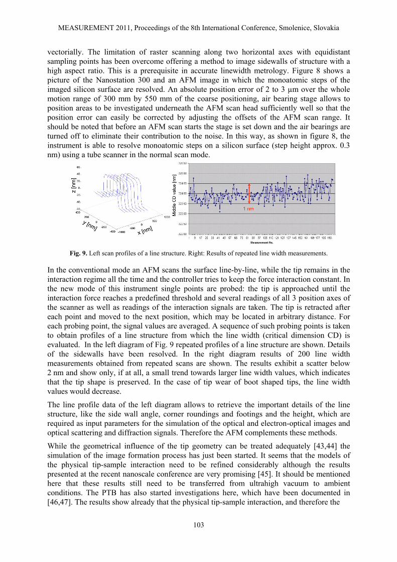
Fig. 9. Left scan profiles of a line structure. Right: Results of repeated line width measurements.
In the conventional mode an AFM scans the surface line-by-line, while the tip remains in the interaction regime all the time and the controller tries to keep the force interaction constant. In the new mode of this instrument single points are probed: the tip is approached until the interaction force reaches a predefined threshold and several readings of all 3 position axes of the scanner as well as readings of the interaction signals are taken. The tip is retracted after each point and moved to the next position, which may be located in arbitrary distance. For each probing point, the signal values are averaged. A sequence of such probing points is taken to obtain profiles of a line structure from which the line width (critical dimension CD) is evaluated. In the left diagram of Fig. 9 repeated profiles of a line structure are shown. Details of the sidewalls have been resolved. In the right diagram results of 200 line width measurements obtained from repeated scans are shown. The results exhibit a scatter below 2 nm and show only, if at all, a small trend towards larger line width values, which indicates that the tip shape is preserved. In the case of tip wear of boot shaped tips, the line width values would decrease.
The line profile data of the left diagram allows to retrieve the important details of the line structure, like the side wall angle, corner roundings and footings and the height, which are required as input parameters for the simulation of the optical and electron-optical images and optical scattering and diffraction signals. Therefore the AFM complements these methods.
While the geometrical influence of the tip geometry can be treated adequately [43,44] the simulation of the image formation process has just been started. It seems that the models of the physical tip-sample interaction need to be refined considerably although the results presented at the recent nanoscale conference are very promising [45]. It should be mentioned here that these results still need to be transferred from ultrahigh vacuum to ambient conditions. The PTB has also started investigations here, which have been documented in [46,47]. The results show already that the physical tip-sample interaction, and therefore the
MEASUREMENT 2011, Proceedings of the 8th International Conference, Smolenice, Slovakia
104
image signal of the AFM, changes drastically at steep sidewalls. Conclusion
The PTB has a strong commitment to both, dimensional micro- and nanotechnology. To be able to perform dimensional measurements at the highest level of accuracy requires specialized and often especially developed instruments and a complete understanding of measurement signals including the interaction of probe and sample. The assumption that this interaction does not vary during the coarse of the measurement is no longer justified.
References
[1] Brand U, Kirchhoff J. A micro-CMM with metrology frame for low uncertainty measurements Measurement Science and Technology 16: 2489-2497, 2005.
[2] Küng A, Meli F, Thalmann R. Ultraprecision micro-CMM using a low force 3D touch probe Measurement Science and Technology 18(1):319-327,2007
[3] Van Seggelen J K, Rosielle P C J N, Schellekens, P H J. Design of a 3-D CMM with elasticall guided z-axis and x-y-axis with less than 2 mm Abbe offset. In proceedings of 3rd Euspen conference,2002, 29-32
[4] Ji G, Schwenke H, Trapet E. Opto-tactile sensor for measuring small structures on coordinate measuring machines. In Proceeding of the annual meeting of the American Society for Precision Engineering, 1998, 25-28.
[5] Neuschaefer-Rube U, Wissmann M. PTB-Mitteilungen 117(4):390–396,2007 (in German)
[6] Dai G, Bütefisch S, Pohlenz F, Danzebrink H U. A high precision micro/nano CMM using piezoresistive tactile probes. Measurement Science and Technology 20: 084001-084010, 2009
[7] Dai G, Wolf H, Weinmann T, Xu M, Pohlenz F, Danzebrink H U. Nanoscale surface measurements at sidewalls of nano- and micro-structurres. Measurement Science and Technology 18: 334-341, 2007.
[8] Nesterov V, Brand U. Modelling and investigation of the mechanical and electrical characteristics of the silicon 3D-boss microprobe for force and deflection measurements. J. Micromech. Microengineering 16: 1116–1127, 2006
[9] Nesterov V. Facility and methods for the measurement of micro and nano forces in the range below 10-5 N with a resolution of 10-12 N (development concept). Measurement Science and Technology 18: 360-366, 2007.
[10] Nesterov V, Mueller M, Frumin L, Brand U. A new facility to realize a nanonewton force standard based on electrostatic methods. Metrologia 46:277-282,2009
[11] Bartscher C M, Hilpert U, Goebbels J, Weidemann G. Enhancement and Proof of Accuracy of Industrial Computed Tomography(CT) Measurements. CIRP Annals-Manufactoring Technology 56(1):495 -498, 2007
[12] Dai G, Pohlenz F, Danzebrink H.U, Xu M, Hasche K, Wilkening G. Metrological large range scanning probe microscope. Review of Scientific. Instruments 75:962–969, 2004
[13] Ritter M, Dziomba T, Kranzmann A, Koenders L. A landmark-based 3D calibration strategy for SPM Measurement Science and Technology 18 (2): 404 – 414,2007
[14] http://www.iso.org and links to the scope of ISO TC 229 on ‘Nanotechnology’
MEASUREMENT 2011, Proceedings of the 8th International Conference, Smolenice, Slovakia
105
[15] Thomsen-Schmidt P. Characterization of a traceable profiler instrument for areal roughness measurements. In Proceedings of Nanoscale 2010, to be published in special issue of Measurement Science and Technology.
[16] Köning R, Flügge J, Bosse H. Recent activities at PTB nanometer comparator In Proceedings of the Conference on Recent Developments in Traceable Dimensional Measurements, 2003,SPIE, Vol. 5190, 391-399
[17] Köning R, Flügge J, Bosse H. Achievement of sub nanometer reproducibility with the Nanometer Comparator. In Proceedings of the Advanced Lithography Conference, 2007, SPIE 6518, 65183F-1 - 65183F-8
[18] Schödel, R, Abou-Zeid, A. PTB’s precision interferometer for high accuracy characterization of thermal expansion properties of low expansion materials, In: Nanoscale calibration standards and methods: dimensional and related measurements in the micro- and nanometer range, Wilkening, G. and Koenders, L., eds.; ISBN 3-527-40502-X; ISBN 978-3-527-40502-2, pp. 500 - 514 (2005)
[19] Geckeler R D. Optimal use of pentaprism in gighly accurate deflectometric scanning. Measurement Science and Technology 18(1): 115-125, 2007.
[20] Just A, Krause M, Probst R Wittekopf R. Calibration of high-resolution electronic autocollimators against an angle comparator. Metrologia 40:288-294, 2003.
[21] Ehret G, Pilarski F, Bergmann D, Bodermann B Buhr E. A new high-aperture 193 nm microscope for the traceable dimensional characterization of micro- and nanostructures Measurement Science and Technology 20(6):084010-084020, 2009
[22] Wurm M, Pilarski F, Bodermann B. A new flexible scatterometer for critical dimension metrology. Review of Scientific Instruments 81: 023701- 023709, 2010
[23] Bodermann, B Ehret G. Comparison of different approaches for modelling microscope images on the basis of rigorous diffraction calculation. In, Proceedings of SPIE 5858, 2005, 09-1 - 09-12
[24] Gross H, Model R, Bär M, Wurm M, Bodermann B, Rathsfeld. A Mathematcial Modeling of indirect measurements in scatterometry Measurement 39 (9): 782–794, 2006.
[25] Scholze F, Laubis C; Ulm G, Dersch U; Pomplun J, Burger S,; Schmidt F. In Proc. of Advanced Lithography Conference, 2008,SPIE 6921,69213R-1 - 69213R-11.
[26] Garnaes J, Dirscherl K. NANO5-2D-Grating-Final report, Metrologia 45:04003, 2008.
[27] Decker J E, Buhr E, Diener A, Eves B Kueng A, Meli F Pekelsky J R, Pan S-P, Yao B-C. Report on an international comparison on one-dimensional (1D) grating pitch Metrologia 46: 04001,2009
[28] Frase C. G. Haessler-Grohne W. Use of Monte Carlo models in the development and validation of CD operators. Surface and Interface Analysis 37(11):11, 942 – 950,2005
[29] Richter J, Heins T, Liebe R, Bodermann B, Diener A, Bergmann D, Frase C G, Bosse H. Calibration of CD mask standards for the 65 nm node:CoG and MoSi. In Proceedings of the 23rd European Mask & Lithography Conference.2007, SPIE 6533, 6533-53
[30] Buhr E, Senftleben N, Klein T, Bergmann D, Gnieser D, Frase C G, Bosse H. Characterization of nanoparticles by scanning electron microscopy in transmission mode. Measurement Science and Technology 20:084025 (9p), 2009
[31] Zhao X. Scanning Probe Microscopes with High resolution capacitive transducers PTB Report, PTB-F-32, ISBN 3-89701-207-3,1998
MEASUREMENT 2011, Proceedings of the 8th International Conference, Smolenice, Slovakia
106
[32] Jusko O, Zhao X, Wolff H,Wilkening G. Design and three dimensional calibration of a measuring scanning tunneling microscope. Review of Scientific Instruments 65(8):2514-2518,1994
[33] B. Barbato, K. Carneiro, J. Garnæs, G. Gori, G. Hughes, C. Jensen, J.F. Jørgensen, O. Jusko, Livi, H. McQuoid, L. Nielsen, G.B. Picotto, G. Wilkening. Scanning Tunneling Microscopy Methods for Roughness and Micro Hardness Measurements. Synthesis Report on BCR project 3423/2/0/284/4/92-BCR-DK(30), (1994)
[34] Danzebrink, H. U, Nahfeldmikroskopischer Sensor mit interner Signalwandlung. PTB report, PTB-F-27, ISBN 3-89439-830-8
[35] Köning R, Jusko O, Koenders L, Schlachetzki. A Systematic Investigation.of Nanostructuring by STM. Journal of Vacuum Science and Technology B14: 48 -53, 1996
[36] Koenders L, Harms C H, Waltereit E, Wilkening G. An ultra-precision interference comparator for dimensional measurements using two tunnelling microscopes as probes. Measurement Science and Technology 14(6):943-952, 2003
[37] Hasche K, Herrmann K, Mirande W, Pohlenz F, Seemann R. Development of Scanning Force Microscopy with Subnanometric Capability. In Proceedings of 4th seminar of quantitative microscopy,2000, PTB report (PTB-F-39),219-225
[38] Discherl K, Cerkas S, Bosse H, Fuß H A. The Nanostation 300 – Development of an SPM for large objects, unpublished
[39] Yacoot A, Kuetgens U, Koenders L, Weimann T. A combined scanning tunnelling microscope and x-ray interferometer. Measurement Science and Technology 12(8):1660-1665, 2001
[40] Yacoot A, Koenders L. From nanometre to millimetre: a feasibility study of the combination of scanning probe microscopy and combined optical and x-ray interferometry. Measurement Science and Technology 14(8):N59-N63, 2003
[41] Yacoot A, Koenders L, Wolff H. An atomic force microscope for the study of the effect of tip sample interaction on dimensional metrology. Measurement Science and Technolog 18 350–9
[42] Strube S, Molnar G, Danzebrink H-U. Compact FPGA based multi-axial interferometer for simultaneous tilt and distance measurement in the sub-nanometre range. In Proceedins of Nanoscale 2010, to be published in a special issue of Measurement Science and Technology.
[43] Villarrubia J S. Algorithms for scanned probe microscope image simulation, surface reconstruction and tip estimation. Journal of Research of the National Institute of Standards and Technology 102:245-254, 1997
[44] Williams P, Williams P M, Shakesheff K M, Davies M C, Jackson D E,Roberts C J and Tendler S J B. Blind reconstruction of scanning probe image data. J. Vac. Sci. Technol. B 14:1577–62, 1996a
[45] Sugimoto Y, Pou P, Abe M, Jellinek P, Perez R, Morita S, Custance O. Chemical identification of individual surface atoms by atomic force microscopy. Nature 446(1):64-67,2007
[46] Yacoot A, Koenders L. Aspects of scanning force microscope probes and their effects on dimensional meaurements. Applied Physics 41(8):103001-103047, 2008
[47] Hüser-Espig D, Haessler Grohne W, Dai G, Bosse H. Investigation of cantilever response of NC-AFM in measuring true 3D structures. In proceedings of Nanoscale 2010 to be published in a special issue of Measurement Science and Technology