Department of EECS EE100/42-43 Spring 2007 Rev. 1 Diodes and Transistors 1. Introduction So far in EE100 you have seen analog circuits. You started with simple resistive circuits, then dynamical systems (circuits with capacitors and inductors) and then op-amps. Then you learned how circuit elements do not operate the same at all frequencies. Now you will learn about two very important circuit elements – diodes 1 and transistors. These elements make the world of digital electronics “tick”. Digital electronics has revolutionized industry over the last 40 years. In the second half of this course, you will learn some of the fundamental concepts (Boolean algebra, microcontrollers, processor I/O and digital systems interfacing) behind this revolution. However, before you do so, you should understand the two devices – diodes and transistors – that were responsible for this revolution. 2. Organization of this document In this document, we will talk about diodes and transistors. First we will discuss very basic semiconductor physics. We won’t discuss the details because the point of this course is electronic circuits, not semiconductor physics. A detailed understanding of semiconductor physics is important only when you deal with microelectronic circuits. We are just building breadboard circuits in this class, thus it is enough if you have an intuitive understanding of the semiconductor physics. If you want to learn the detailed physics behind these devices, you should consider taking EECS 130 at the University of California, Berkeley. Next we will talk about diodes, followed by the bipolar junction transistor. In the case of both devices, we will talk about the nonlinear models, load line analysis and applications. We will conclude this chapter by looking at how transistors can be used as logic devices. This will lead naturally to our discussion of digital systems. Please note that I have chosen to discuss the bipolar junction transistor instead of the field effect transistor. The reason: bipolar transistors are the mainstay of interface elements to microcontrollers. Thus you will be seeing a lot of BJTs when you work with sensor interfaces. 3. Basic Semiconductor Physics [4] [2] [6] A semiconductor is a solid whose electrical conductivity is in between that of a metal and that of an insulator, and can be controlled over a wide range, either permanently or dynamically. Semiconductors are tremendously important technologically and 1 Diodes are really not used in digital circuits anymore. However they are fundamental in circuits like power electronics. Moreover, they are simpler to understand than transistors. So we start our discussion of nonlinear electronics with diodes.
Transcript
Department of EECS EE100/42-43 Spring 2007 Rev. 1
Diodes and Transistors
1. Introduction So far in EE100 you have seen analog circuits. You started with simple resistive circuits, then dynamical systems (circuits with capacitors and inductors) and then op-amps. Then you learned how circuit elements do not operate the same at all frequencies. Now you will learn about two very important circuit elements – diodes1 and transistors. These elements make the world of digital electronics “tick”. Digital electronics has revolutionized industry over the last 40 years. In the second half of this course, you will learn some of the fundamental concepts (Boolean algebra, microcontrollers, processor I/O and digital systems interfacing) behind this revolution. However, before you do so, you should understand the two devices – diodes and transistors – that were responsible for this revolution. 2. Organization of this document In this document, we will talk about diodes and transistors. First we will discuss very basic semiconductor physics. We won’t discuss the details because the point of this course is electronic circuits, not semiconductor physics. A detailed understanding of semiconductor physics is important only when you deal with microelectronic circuits. We are just building breadboard circuits in this class, thus it is enough if you have an intuitive understanding of the semiconductor physics. If you want to learn the detailed physics behind these devices, you should consider taking EECS 130 at the University of California, Berkeley. Next we will talk about diodes, followed by the bipolar junction transistor. In the case of both devices, we will talk about the nonlinear models, load line analysis and applications. We will conclude this chapter by looking at how transistors can be used as logic devices. This will lead naturally to our discussion of digital systems. Please note that I have chosen to discuss the bipolar junction transistor instead of the field effect transistor. The reason: bipolar transistors are the mainstay of interface elements to microcontrollers. Thus you will be seeing a lot of BJTs when you work with sensor interfaces. 3. Basic Semiconductor Physics [4] [2] [6]
A semiconductor is a solid whose electrical conductivity is in between that of a metal and that of an insulator, and can be controlled over a wide range, either permanently or dynamically. Semiconductors are tremendously important technologically and
1 Diodes are really not used in digital circuits anymore. However they are fundamental in circuits like power electronics. Moreover, they are simpler to understand than transistors. So we start our discussion of nonlinear electronics with diodes.
Department of EECS EE100/42-43 Spring 2007 Rev. 1
economically. Silicon is used to create the most semiconductors commercially but dozens of other materials are used as well.
Semiconductor devices, electronic components made of semiconductor materials, are essential in modern electrical devices, from computers to cellular phones to digital audio players.
Elemental or intrinsic semiconductors are materials consisting of elements from group IV of the periodic table. Figure 1 below depicts the lattice arrangement for silicon (Si), one of the more common semiconductors. At sufficiently high temperatures, thermal energy causes the atoms in the lattice to vibrate; when sufficient kinetic energy is present, some of the valence electrons break their bonds with the lattice structure and become available as conduction electrons. These free electrons enable current flow in a semiconductor.
Figure 1. Lattice structure of silicon However, if you have to heat up a semiconductor for electron flow, then how can it be used at room temperature? The answer to this is: doping. Doping consists of adding impurities to the crystalline structure of the semiconductor. For example, if we add phosphorous atoms to silicon, then we will have an extra electron floating around in the lattice because phosphorous has five valence electrons. Thus phosphorous atoms are also called donors, refer to figure 2. A doped semiconductor is also called as an extrinsic semiconductor. Silicon doped with donors is also called n-type semiconductor because of the abundance of electrons.
Department of EECS EE100/42-43 Spring 2007 Rev. 1
Figure 2. Silicon doped with phosporous There is another kind of conduction that can take place in semiconductors. Suppose we dope silicon with elements from group III of the periodic table, say boron. This is shown in figure 3. Now we have some missing orbitals or places where electrons can go. Thus the electrons are moving to the left. The vacancy caused by the departure of a free electron is called a hole. Note that whenever a hole is present, we have, in effect a positive charge. The positive charges also contribute to the conduction process, in the sense that if an electron “jumps” to fill a neighboring hole, thereby neutralizing a positive charge, it correspondingly creates a new hole at a neighboring location. Because elements from group III of the periodic table “accept electrons”, they are also called acceptors. Silicon doped with acceptors is also called a p-type semiconductor because of the abundance of holes.
Figure 3. Silicon doped with boron. The movement of an electron to the left is equivalent to a hole
moving to the right. It is important to point out here that mobility – that is, the ease with which charge carriers move across the lattice differs greatly for electrons and holes. In the case of silicon doped with phosphorous, we have free electrons in the lattice that can move easily. In contrast, when silicon is doped with boron, holes move only if a neighboring electron jumps to fill the empty bond.
Department of EECS EE100/42-43 Spring 2007 Rev. 1
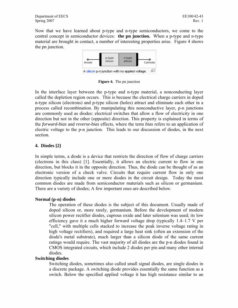
Now that we have learned about p-type and n-type semiconductors, we come to the central concept in semiconductor devices: the pn junction. When a p-type and n-type material are brought in contact, a number of interesting properties arise. Figure 4 shows the pn junction.
Figure 4. The pn junction In the interface layer between the p-type and n-type material, a nonconducting layer called the depletion region occurs. This is because the electrical charge carriers in doped n-type silicon (electrons) and p-type silicon (holes) attract and eliminate each other in a process called recombination. By manipulating this nonconductive layer, p-n junctions are commonly used as diodes: electrical switches that allow a flow of electricity in one direction but not in the other (opposite) direction. This property is explained in terms of the forward-bias and reverse-bias effects, where the term bias refers to an application of electric voltage to the p-n junction. This leads to our discussion of diodes, in the next section. 4. Diodes [2] In simple terms, a diode is a device that restricts the direction of flow of charge carriers (electrons in this class) [1]. Essentially, it allows an electric current to flow in one direction, but blocks it in the opposite direction. Thus, the diode can be thought of as an electronic version of a check valve. Circuits that require current flow in only one direction typically include one or more diodes in the circuit design. Today the most common diodes are made from semiconductor materials such as silicon or germanium. There are a variety of diodes; A few important ones are described below. Normal (p-n) diodes
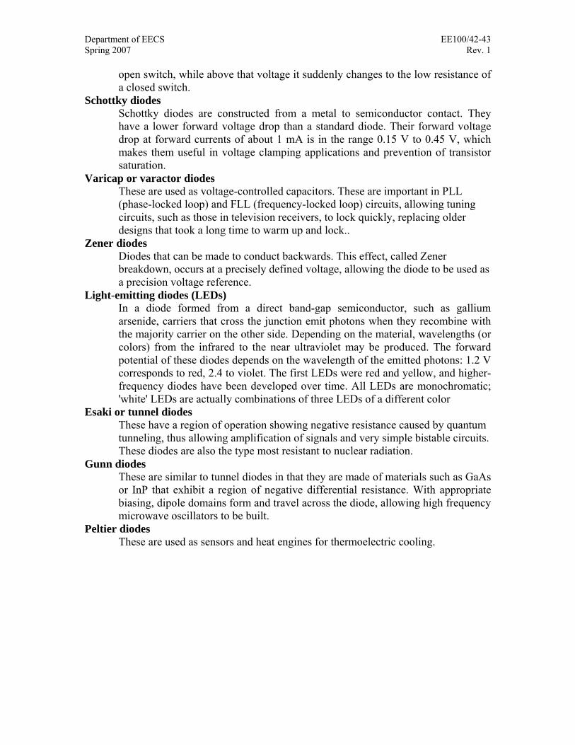
The operation of these diodes is the subject of this document. Usually made of doped silicon or, more rarely, germanium. Before the development of modern silicon power rectifier diodes, cuprous oxide and later selenium was used; its low efficiency gave it a much higher forward voltage drop (typically 1.4–1.7 V per "cell," with multiple cells stacked to increase the peak inverse voltage rating in high voltage rectifiers), and required a large heat sink (often an extension of the diode's metal substrate), much larger than a silicon diode of the same current ratings would require. The vast majority of all diodes are the p-n diodes found in CMOS integrated circuits, which include 2 diodes per pin and many other internal diodes.
Switching diodes Switching diodes, sometimes also called small signal diodes, are single diodes in a discrete package. A switching diode provides essentially the same function as a switch. Below the specified applied voltage it has high resistance similar to an
Department of EECS EE100/42-43 Spring 2007 Rev. 1
open switch, while above that voltage it suddenly changes to the low resistance of a closed switch.
Schottky diodes Schottky diodes are constructed from a metal to semiconductor contact. They have a lower forward voltage drop than a standard diode. Their forward voltage drop at forward currents of about 1 mA is in the range 0.15 V to 0.45 V, which makes them useful in voltage clamping applications and prevention of transistor saturation.
Varicap or varactor diodes These are used as voltage-controlled capacitors. These are important in PLL (phase-locked loop) and FLL (frequency-locked loop) circuits, allowing tuning circuits, such as those in television receivers, to lock quickly, replacing older designs that took a long time to warm up and lock..
Zener diodes Diodes that can be made to conduct backwards. This effect, called Zener breakdown, occurs at a precisely defined voltage, allowing the diode to be used as a precision voltage reference.
Light-emitting diodes (LEDs) In a diode formed from a direct band-gap semiconductor, such as gallium arsenide, carriers that cross the junction emit photons when they recombine with the majority carrier on the other side. Depending on the material, wavelengths (or colors) from the infrared to the near ultraviolet may be produced. The forward potential of these diodes depends on the wavelength of the emitted photons: 1.2 V corresponds to red, 2.4 to violet. The first LEDs were red and yellow, and higher-frequency diodes have been developed over time. All LEDs are monochromatic; 'white' LEDs are actually combinations of three LEDs of a different color
Esaki or tunnel diodes These have a region of operation showing negative resistance caused by quantum tunneling, thus allowing amplification of signals and very simple bistable circuits. These diodes are also the type most resistant to nuclear radiation.
Gunn diodes These are similar to tunnel diodes in that they are made of materials such as GaAs or InP that exhibit a region of negative differential resistance. With appropriate biasing, dipole domains form and travel across the diode, allowing high frequency microwave oscillators to be built.
Peltier diodes These are used as sensors and heat engines for thermoelectric cooling.
Department of EECS EE100/42-43 Spring 2007 Rev. 1
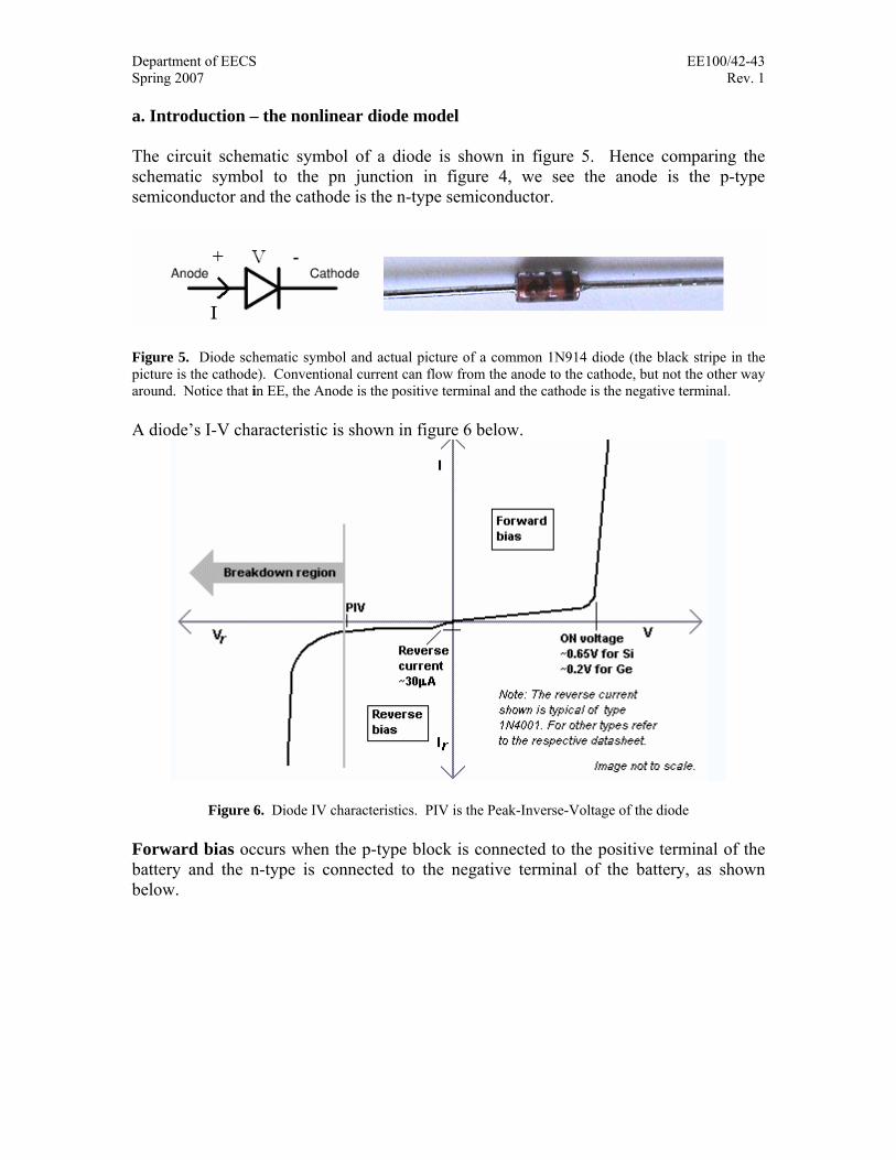
a. Introduction – the nonlinear diode model The circuit schematic symbol of a diode is shown in figure 5. Hence comparing the schematic symbol to the pn junction in figure 4, we see the anode is the p-type semiconductor and the cathode is the n-type semiconductor.
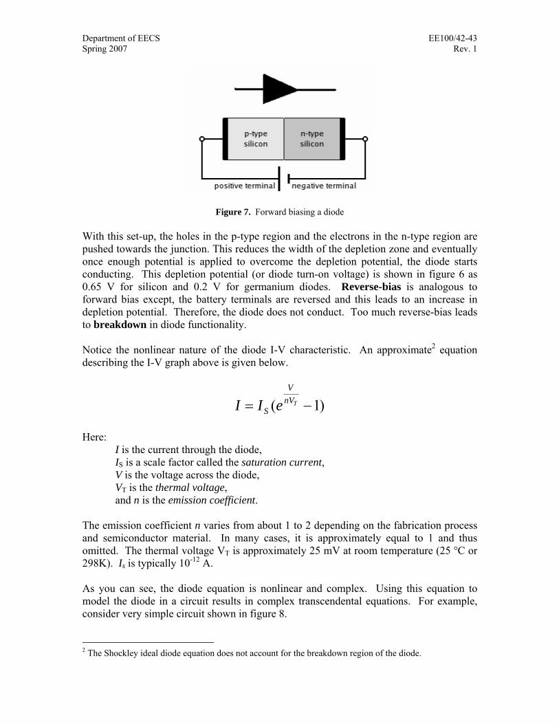
Figure 5. Diode schematic symbol and actual picture of a common 1N914 diode (the black stripe in the picture is the cathode). Conventional current can flow from the anode to the cathode, but not the other way around. Notice that in EE, the Anode is the positive terminal and the cathode is the negative terminal. A diode’s I-V characteristic is shown in figure 6 below.
Figure 6. Diode IV characteristics. PIV is the Peak-Inverse-Voltage of the diode Forward bias occurs when the p-type block is connected to the positive terminal of the battery and the n-type is connected to the negative terminal of the battery, as shown below.
Department of EECS EE100/42-43 Spring 2007 Rev. 1
Figure 7. Forward biasing a diode With this set-up, the holes in the p-type region and the electrons in the n-type region are pushed towards the junction. This reduces the width of the depletion zone and eventually once enough potential is applied to overcome the depletion potential, the diode starts conducting. This depletion potential (or diode turn-on voltage) is shown in figure 6 as 0.65 V for silicon and 0.2 V for germanium diodes. Reverse-bias is analogous to forward bias except, the battery terminals are reversed and this leads to an increase in depletion potential. Therefore, the diode does not conduct. Too much reverse-bias leads to breakdown in diode functionality. Notice the nonlinear nature of the diode I-V characteristic. An approximate2 equation describing the I-V graph above is given below.
)1( −= TnVV
S eII Here:
I is the current through the diode, IS is a scale factor called the saturation current, V is the voltage across the diode, VT is the thermal voltage, and n is the emission coefficient.
The emission coefficient n varies from about 1 to 2 depending on the fabrication process and semiconductor material. In many cases, it is approximately equal to 1 and thus omitted. The thermal voltage VT is approximately 25 mV at room temperature (25 ±C or 298K). Is is typically 10-12 A. As you can see, the diode equation is nonlinear and complex. Using this equation to model the diode in a circuit results in complex transcendental equations. For example, consider very simple circuit shown in figure 8. 2 The Shockley ideal diode equation does not account for the breakdown region of the diode.
Department of EECS EE100/42-43 Spring 2007 Rev. 1
Figure 8. Simple diode circuit Using KVL:
)1000))(1((
)1000( 12
1
1
1
11
−+=
+=+=
T
D
nVV
SD
D
RD
eIV
iVVV
You can solve the last equation above using a tool like Mathematica:
Mathematica gives a value of approximately 0.58 V for the voltage and 11.42 mA for the current. However the point of this exercise is that you cannot solve the equation above without a calculator. Therefore we will now introduce a very important graphical method to solve circuits – load lines. b. Load line Analysis Consider the circuit in figure 8 again. We know the diode I-V is given by:
(1) )1)(10( 025.0121
−= −DV
D eI Using KVL and Ohm’s law:
1 112
1
1
RIViRV
DD
D
+=+=
Note the current going through the diode, resistor and voltage source is the same. This is the key to load lines. It enables us to impose another restriction on the (VD1,ID) pair:
Department of EECS EE100/42-43 Spring 2007 Rev. 1
(2) 1
12 1
RVI D
D−
=
Graphically, we can plot (1) and (2) on the same set of axis. This is done in figure 9 below.
Figure 9. Load line as plotted using MATLAB. Point of intersection is the solution to the system.
The commands to do this in MATLAB are: >> n = 1; >> Vt = 0.025; >> Is = 10^-12; >> VD1 = [-5:0.01:0.6]; >> ID = Is*(exp(VD1/(n*Vt)) - 1); >> plot(VD1,ID); >> hold; >> VD2 = [-5:0.01:12]; >> ID2 = (12-VD2)/R1; >> plot(VD2,ID2); The point of intersection is also called as the Quiescent-point (Q-point) or DC operating point of the system. Thus load lines are a graphical way to solve circuits. Notice that load lines are very useful when a circuit has a single nonlinear element. Although you could use the method when the circuit has multiple nonlinear elements, it becomes tricky.
Department of EECS EE100/42-43 Spring 2007 Rev. 1
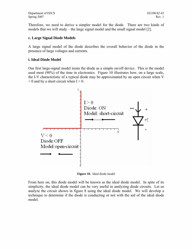
Therefore, we need to derive a simpler model for the diode. There are two kinds of models that we will study – the large signal model and the small signal model [2]. c. Large Signal Diode Models A large signal model of the diode describes the overall behavior of the diode in the presence of large voltages and currents. i. Ideal Diode Model Our first large-signal model treats the diode as a simple on/off device. This is the model used most (90%) of the time in electronics. Figure 10 illustrates how, on a large scale, the I-V characteristic of a typical diode may be approximated by an open circuit when V < 0 and by a short circuit when I > 0.
Figure 10. Ideal diode model From here on, this diode model will be known as the ideal diode model. In spite of its simplicity, the ideal diode model can be very useful in analyzing diode circuits. Let us analyze the circuit shown in figure 8 using the ideal diode model. We will develop a technique to determine if the diode is conducting or not with the aid of the ideal diode model.
Department of EECS EE100/42-43 Spring 2007 Rev. 1
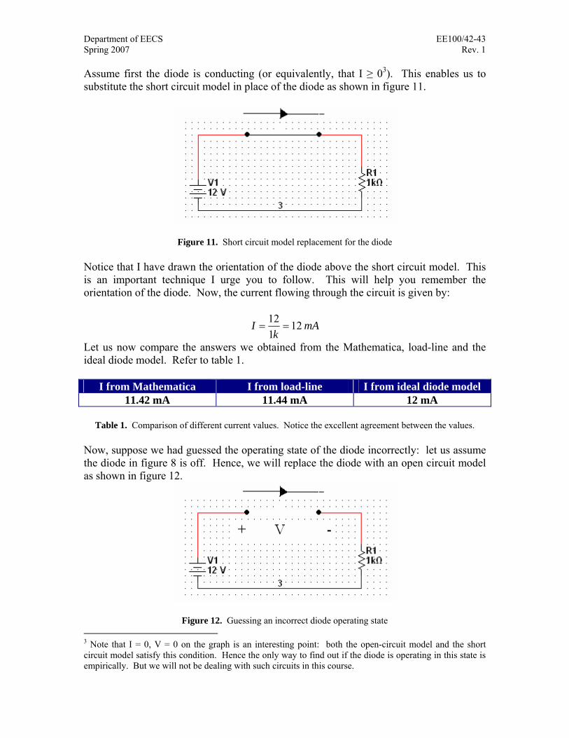
Assume first the diode is conducting (or equivalently, that I ≥ 03). This enables us to substitute the short circuit model in place of the diode as shown in figure 11.
Figure 11. Short circuit model replacement for the diode Notice that I have drawn the orientation of the diode above the short circuit model. This is an important technique I urge you to follow. This will help you remember the orientation of the diode. Now, the current flowing through the circuit is given by:
mAk
I 12112
==
Let us now compare the answers we obtained from the Mathematica, load-line and the ideal diode model. Refer to table 1.
I from Mathematica I from load-line I from ideal diode model 11.42 mA 11.44 mA 12 mA
Table 1. Comparison of different current values. Notice the excellent agreement between the values.
Now, suppose we had guessed the operating state of the diode incorrectly: let us assume the diode in figure 8 is off. Hence, we will replace the diode with an open circuit model as shown in figure 12.
Figure 12. Guessing an incorrect diode operating state 3 Note that I = 0, V = 0 on the graph is an interesting point: both the open-circuit model and the short circuit model satisfy this condition. Hence the only way to find out if the diode is operating in this state is empirically. But we will not be dealing with such circuits in this course.
Department of EECS EE100/42-43 Spring 2007 Rev. 1
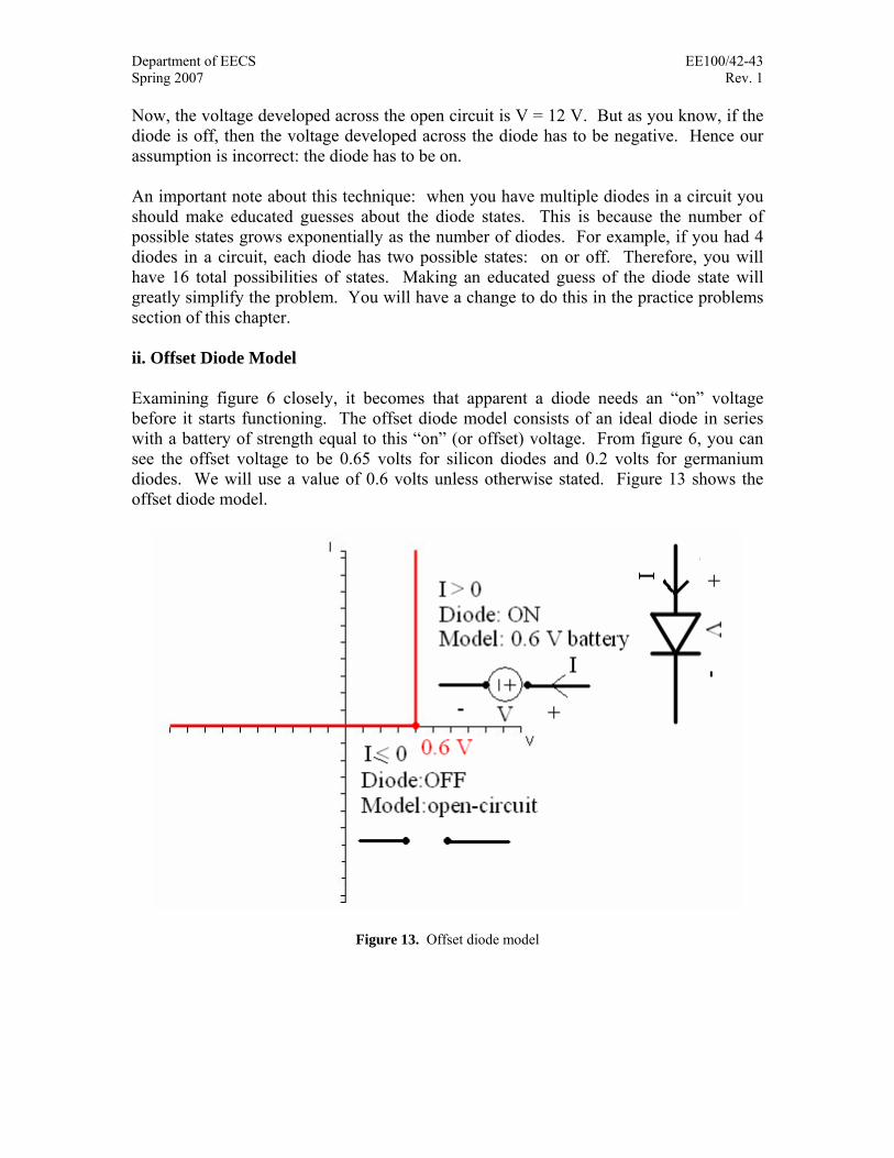
Now, the voltage developed across the open circuit is V = 12 V. But as you know, if the diode is off, then the voltage developed across the diode has to be negative. Hence our assumption is incorrect: the diode has to be on. An important note about this technique: when you have multiple diodes in a circuit you should make educated guesses about the diode states. This is because the number of possible states grows exponentially as the number of diodes. For example, if you had 4 diodes in a circuit, each diode has two possible states: on or off. Therefore, you will have 16 total possibilities of states. Making an educated guess of the diode state will greatly simplify the problem. You will have a change to do this in the practice problems section of this chapter. ii. Offset Diode Model Examining figure 6 closely, it becomes that apparent a diode needs an “on” voltage before it starts functioning. The offset diode model consists of an ideal diode in series with a battery of strength equal to this “on” (or offset) voltage. From figure 6, you can see the offset voltage to be 0.65 volts for silicon diodes and 0.2 volts for germanium diodes. We will use a value of 0.6 volts unless otherwise stated. Figure 13 shows the offset diode model.
Figure 13. Offset diode model
Department of EECS EE100/42-43 Spring 2007 Rev. 1
d. Diode Exercises4 1. Determine the operating point of the diode in figure 14 below and compute the power output of the 12 V battery. The I-V graph of the 1N914 diode is given in figure 15. Hint: Find the Thevenin equivalent seen by the diode and use a load line to find the Q-point. Once you find the diode current and voltage, you can solve for the current through the battery to find the power output.
Figure 14. Simple circuit with one diode
Figure 15. 1N914 I-V characteristic
4These examples are from other textbooks and online sources. Due to a lack of time, we (me and the TAs) are not posting solutions to the problems. If you can email the answers (and complete solutions) to me, I will post it on the website (with proper credits).
Department of EECS EE100/42-43 Spring 2007 Rev. 1
2. Determine the voltage across and current through the diode in figure 16. Assume the diode is ideal.
Figure 16. Circuit for problem 2
3. [Diode Logic] This problem shows you can build logic gates out of diodes. You will learn about logic gates when we talk about digital systems. For the circuit below, fill in the table for the value Vx given the different combinations of values for V1 and V2. Assume the diodes are ideal.
Figure 17. Diode logic gate
V1 (volts) V2 (volts) Vx (volts)
0 0 0 5 5 0 5 5
Table 2. Diode “truth” table
4. [Diode Rectifier] The circuit below can be used to convert an AC voltage to DC. Assuming V1(t) = 5sin(2p60t) volts, sketch Vx(t). USE THE OFFSET DIODE MODEL in your analysis. Assume the circuit has been in operation for a long time (i.e. assume all the transients have died out).
Department of EECS EE100/42-43 Spring 2007 Rev. 1
Figure 18. A very simple AC-DC converter
Note: In a practical AC-DC converter, a 4-diode circuit known as the bridge rectifier is used. There are also Zener diodes at the output for better performance of the AC-DC converter. 5. [Diode Clamp] The circuit below shifts the DC level of a signal. Find and sketch Vx(t).
Figure 19. A diode clamp
Department of EECS EE100/42-43 Spring 2007 Rev. 1
5. Transistors [3] [5] a. Introduction A transistor is a three-terminal semiconductor device that can perform two functions that are fundamental to the design of electronic circuits: amplification and switching. Put simply, amplification consists of magnifying a signal by transferring energy to it from an external source, whereas a transistor switch is a device for controlling a relatively large current between or voltage across two terminals by means of a small control current or voltage applied at a third terminal. There are two main types of transistors: Field-Effect Transistors and Bipolar Junction Transistors. In this course, we will discuss Bipolar Junction Transistors (BJTs). This section in the document is a paraphrase of [3] and [5]. From now on we will use the terms BJT and transistors5 interchangeably. A BJT is formed by joining three sections of semiconductor material, each with a different doping concentration. The three sections can be either a thin n region sandwiched between p+ and p layers, or a p region between n and n+ layers, where the superscript plus indicates more heavily doped material. The resulting BJTs are called pnp and npn transistors, respectively; we discuss only the latter in this document. Figure 20 illustrates the approximate construction, symbols and nomenclature for the two types of BJTs.
Figure 20. The actual shape of a BJT and BJT nomenclature [3] The behavior of npn BJT is discussed below. Operation of a pnp transistor is analogous to that of a npn transistor except that the role of charge carries reversed. In npn transistors,
5 The origin of the term “transistor” will be clear once you understand BJTs
Department of EECS EE100/42-43 Spring 2007 Rev. 1
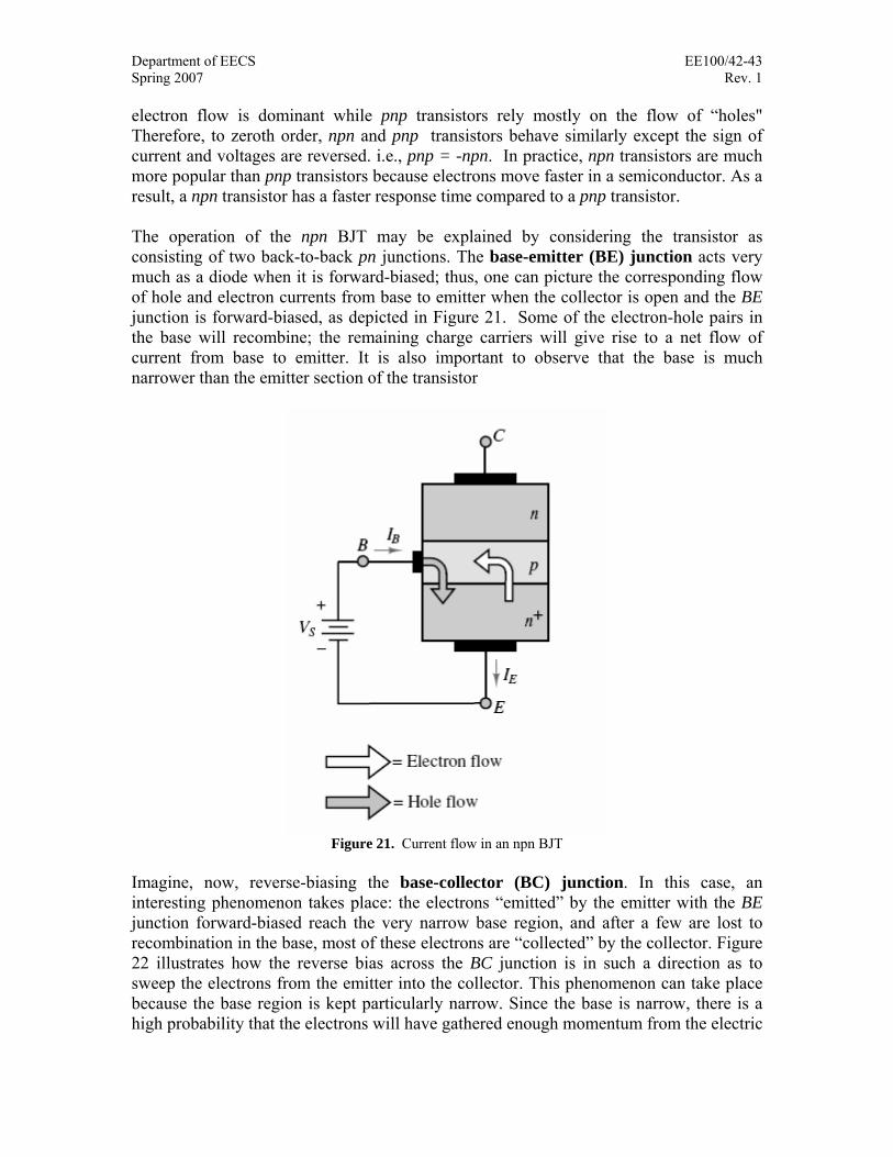
electron flow is dominant while pnp transistors rely mostly on the flow of “holes" Therefore, to zeroth order, npn and pnp transistors behave similarly except the sign of current and voltages are reversed. i.e., pnp = -npn. In practice, npn transistors are much more popular than pnp transistors because electrons move faster in a semiconductor. As a result, a npn transistor has a faster response time compared to a pnp transistor. The operation of the npn BJT may be explained by considering the transistor as consisting of two back-to-back pn junctions. The base-emitter (BE) junction acts very much as a diode when it is forward-biased; thus, one can picture the corresponding flow of hole and electron currents from base to emitter when the collector is open and the BE junction is forward-biased, as depicted in Figure 21. Some of the electron-hole pairs in the base will recombine; the remaining charge carriers will give rise to a net flow of current from base to emitter. It is also important to observe that the base is much narrower than the emitter section of the transistor
Figure 21. Current flow in an npn BJT
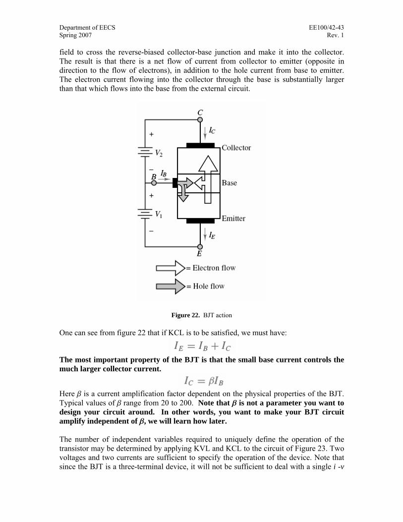
Imagine, now, reverse-biasing the base-collector (BC) junction. In this case, an interesting phenomenon takes place: the electrons “emitted” by the emitter with the BE junction forward-biased reach the very narrow base region, and after a few are lost to recombination in the base, most of these electrons are “collected” by the collector. Figure 22 illustrates how the reverse bias across the BC junction is in such a direction as to sweep the electrons from the emitter into the collector. This phenomenon can take place because the base region is kept particularly narrow. Since the base is narrow, there is a high probability that the electrons will have gathered enough momentum from the electric
Department of EECS EE100/42-43 Spring 2007 Rev. 1
field to cross the reverse-biased collector-base junction and make it into the collector. The result is that there is a net flow of current from collector to emitter (opposite in direction to the flow of electrons), in addition to the hole current from base to emitter. The electron current flowing into the collector through the base is substantially larger than that which flows into the base from the external circuit.
Figure 22. BJT action One can see from figure 22 that if KCL is to be satisfied, we must have:
The most important property of the BJT is that the small base current controls the much larger collector current.
Here b is a current amplification factor dependent on the physical properties of the BJT. Typical values of b range from 20 to 200. Note that b is not a parameter you want to design your circuit around. In other words, you want to make your BJT circuit amplify independent of b, we will learn how later. The number of independent variables required to uniquely define the operation of the transistor may be determined by applying KVL and KCL to the circuit of Figure 23. Two voltages and two currents are sufficient to specify the operation of the device. Note that since the BJT is a three-terminal device, it will not be sufficient to deal with a single i -v
Department of EECS EE100/42-43 Spring 2007 Rev. 1
characteristic; two such characteristics are required to explain the operation of this device. One of these characteristics relates the base current, iB to the base-emitter voltage vBE ; the other relates the collector current iC to the collector-emitter voltage vCE. The latter characteristic actually consists of a family of curves. To determine these I-V characteristics, consider the I-V curves of Figures 24 and 25, using the circuit notation of Figure 23. In Figure 24, the collector is open and the BE junction is shown to be very similar to a diode. The ideal current source IBB injects a base current, which causes the junction to be forward-biased. By varying IBB, one can obtain the open-collector BE junction I-V curve shown in the figure.
Figure 23. Definition of BJT voltages and current
Figure 24. The BE junction open-collector curve
Department of EECS EE100/42-43 Spring 2007 Rev. 1
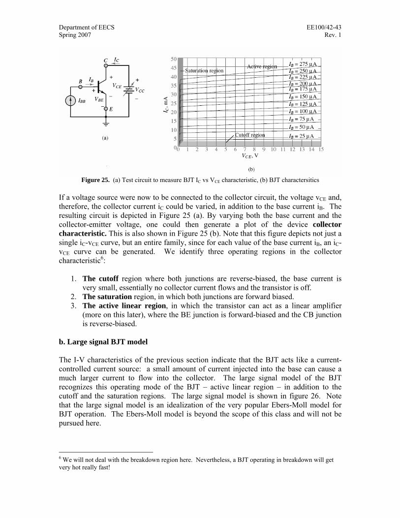
Figure 25. (a) Test circuit to measure BJT IC vs VCE characteristic, (b) BJT charactersitics
If a voltage source were now to be connected to the collector circuit, the voltage vCE and, therefore, the collector current iC could be varied, in addition to the base current iB. The resulting circuit is depicted in Figure 25 (a). By varying both the base current and the collector-emitter voltage, one could then generate a plot of the device collector characteristic. This is also shown in Figure 25 (b). Note that this figure depicts not just a single iC-vCE curve, but an entire family, since for each value of the base current iB, an iC-vCE curve can be generated. We identify three operating regions in the collector characteristic6:
1. The cutoff region where both junctions are reverse-biased, the base current is very small, essentially no collector current flows and the transistor is off.
2. The saturation region, in which both junctions are forward biased. 3. The active linear region, in which the transistor can act as a linear amplifier
(more on this later), where the BE junction is forward-biased and the CB junction is reverse-biased.
b. Large signal BJT model The I-V characteristics of the previous section indicate that the BJT acts like a current-controlled current source: a small amount of current injected into the base can cause a much larger current to flow into the collector. The large signal model of the BJT recognizes this operating mode of the BJT – active linear region – in addition to the cutoff and the saturation regions. The large signal model is shown in figure 26. Note that the large signal model is an idealization of the very popular Ebers-Moll model for BJT operation. The Ebers-Moll model is beyond the scope of this class and will not be pursued here. 6 We will not deal with the breakdown region here. Nevertheless, a BJT operating in breakdown will get very hot really fast!
Department of EECS EE100/42-43 Spring 2007 Rev. 1
Figure 26. BJT large signal model. From now on, Vg will refer to the turn-on voltage of a diode,
approximately 0.7 V. Believe it or not, that is all there is to know about BJTs if you just want to use them as amplifiers or switches. A word of caution: you need to practice a lot of BJT circuits before you are comfortable with them. This is because of the parameterized I-V nature of the BJT characteristic. You have to be really careful of the region of operation of a BJT. Let us do a couple of examples to become comfortable with transistor circuits. We will be use the very common 2N2222A BJT. The I-V graph (from MultiSim) is shown below.
Figure 27. 2N2222A BJT I-V graph
Department of EECS EE100/42-43 Spring 2007 Rev. 1
Example 1: Constant current source. Let us analyze the circuit shown below.
Figure 28. An example of a BJT constant current source
Before we begin analyzing the circuit above, we need to discuss a general methodology to analyzing BJT (or any transistor) circuit:
1. We need to figure out which region of operation the circuit is in. The region of operation depends on the circuit functionality. For instance, in the circuit above, we want the BJT to be in the active region of operation so it can function as a constant current source.
2. Next we set the operating point (DC Bias Point or Q Point from load line terminology) of the transistor to be in the region of operation from step (1).
3. We carry out the analysis to make sure the transistor is operating in the required region of operation (we can use figure 26 as a guide to make sure the voltages and currents are in the correct range).
Let us analyze the circuit in figure 28 using the methodology above. We will use a load line to figure out which region of operation the circuit is in. c. Load line analysis It is simple to plot the load line for the circuit in figure 28. The circuit of interest is our BJT and the BJT I-V characteristic is given in figure 27.
Department of EECS EE100/42-43 Spring 2007 Rev. 1
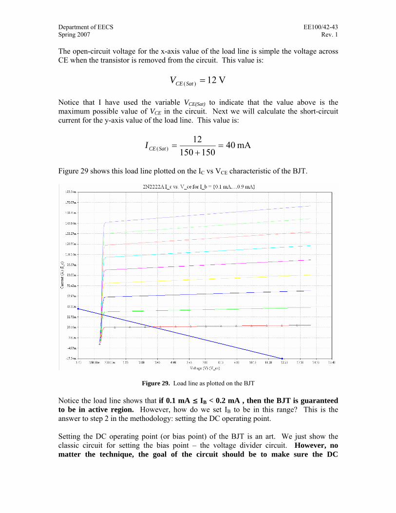
The open-circuit voltage for the x-axis value of the load line is simple the voltage across CE when the transistor is removed from the circuit. This value is:
V 12)( =SatCEV Notice that I have used the variable VCE(Sat) to indicate that the value above is the maximum possible value of VCE in the circuit. Next we will calculate the short-circuit current for the y-axis value of the load line. This value is:
mA 40150150
12)( =
+=SatCEI
Figure 29 shows this load line plotted on the IC vs VCE characteristic of the BJT.
Figure 29. Load line as plotted on the BJT Notice the load line shows that if 0.1 mA £ IB < 0.2 mA , then the BJT is guaranteed to be in active region. However, how do we set IB to be in this range? This is the answer to step 2 in the methodology: setting the DC operating point. Setting the DC operating point (or bias point) of the BJT is an art. We just show the classic circuit for setting the bias point – the voltage divider circuit. However, no matter the technique, the goal of the circuit should be to make sure the DC
Department of EECS EE100/42-43 Spring 2007 Rev. 1
operating point is immune to the changes in b of the BJT. The reason is: b of a transistor can vary by a lot, sometimes there may be a 9:1 variation with current and temperature [7]. This means that is impossible to set a stable Q-point if you rely on b alone. Let us see how the voltage-divider bias helps us set a Q-point independent of b. The term “voltage-divider bias” comes from the voltage divider formed by R1 and R2 in figure 28. The voltage across R2 should forward bias the emitter diode (remember: for the transistor to be in active region, VBE is forward-biased and VCE is reverse-biased). The key point about the voltage divider is the stiffness of the voltage divider. Here is how to get a design guideline for stiffness. If we Thevenize the circuit as shown below, we get the circuit shown in figure 30 below.
Figure 30. Circuit of figure 28 Thevenized at the base terminal. KVL loop for stiffness criterion shown.
Notice that since the transistor is in active region, IC º IE = ICE. Here,
121
2,21
21 VRR
RVthRR
RRRth+
=+
=
We can write a loop equation as shown in figure 30:
04 =−−− RIVRthIVth CEBEB
Department of EECS EE100/42-43 Spring 2007 Rev. 1
Now, βCE
BI
I ≈ . Hence, the equation above becomes:
βRthR
VVthI BE
CE
+
−=
4
If we want to swamp out the effects of b, a good rule of thumb is: R4 is 100 times greater than Rth/b. Thus we want:
401.0 RRth ⋅⋅≤ β Thus, in our circuit: Ω=⋅⋅<Ω= 3301502200.01 250Rth . Hence our circuit should be independent of the changes in b. You should download the MultiSim circuit from the EE100 website and change b to make sure that the circuit is indeed independent of changes in b. You can also confirm the BJT is still in the active region of operation, what is the value of IB? To summarize:
1. Setup a Q-point using a stiff voltage divider and load-line given the current requirements.
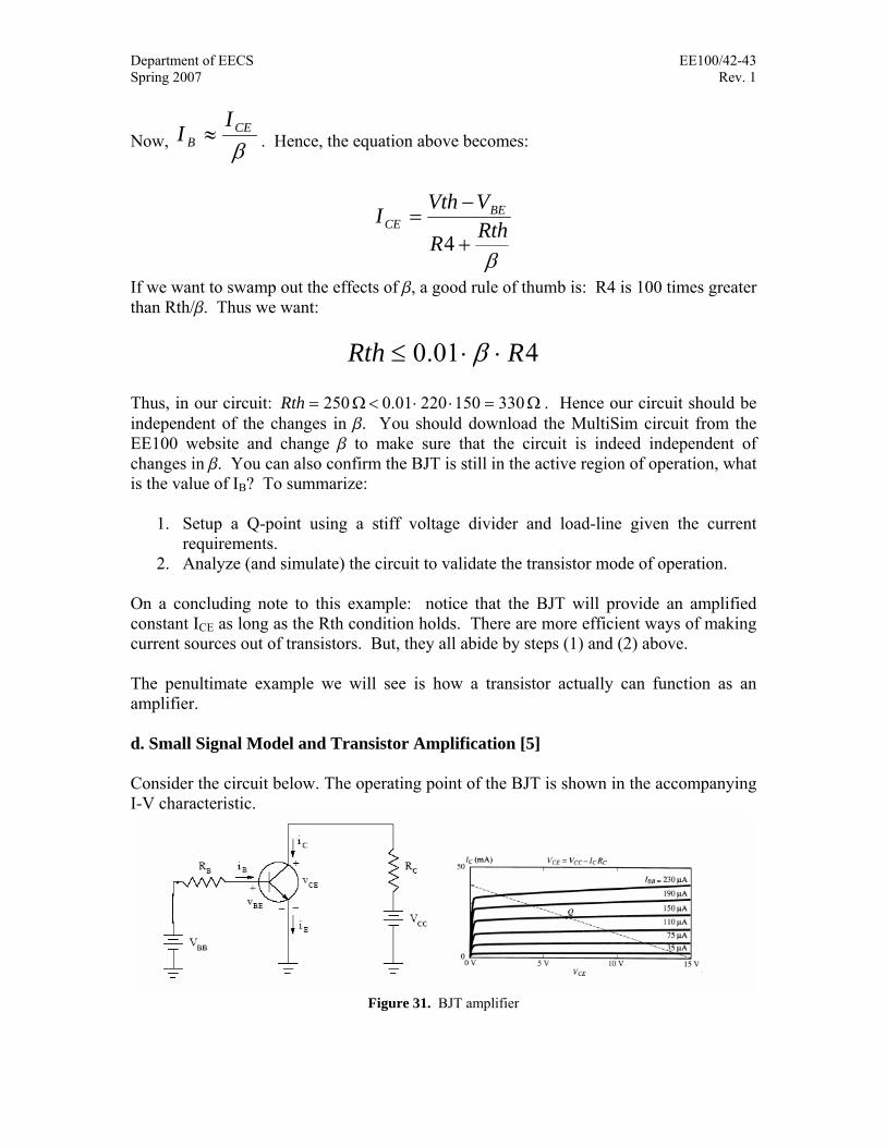
2. Analyze (and simulate) the circuit to validate the transistor mode of operation. On a concluding note to this example: notice that the BJT will provide an amplified constant ICE as long as the Rth condition holds. There are more efficient ways of making current sources out of transistors. But, they all abide by steps (1) and (2) above. The penultimate example we will see is how a transistor actually can function as an amplifier. d. Small Signal Model and Transistor Amplification [5] Consider the circuit below. The operating point of the BJT is shown in the accompanying I-V characteristic.
Figure 31. BJT amplifier
Department of EECS EE100/42-43 Spring 2007 Rev. 1
Let us add a sinusoidal source with an amplitude of DVBB in series with VBB. In response to this additional source, the base current will become iB +DiB leading to the collector current of iC + DiC and CE voltage of VCE + DVCE. These changes are shown in figure 32 below.
Figure 32. Transistor amplifier action They key to how a transistor amplifies: the slope in the active region is small, this implies the resistance (inverse of the slope) is huge. This causes a large voltage drop (notice the large change in VCE) across the CE terminals and thus amplification. Notice that if the transistor falls out of the active region (to saturation), the amplification is lost. Also notice the linear nature of the amplification: there is no distortion in the output signal. This leads to a possibility for a linear model of the BJT in the presence of small voltage changes – this is the small signal model of the BJT. However, a detailed discussion of this model is beyond the scope of this document. Please consult the references at the end of this document for further information. On a concluding note: we have actually designed an amplifier! Nevertheless, a lot of questions still remain about the performance of this amplifier: what range of input frequencies can it handle? Can the BJT source enough output current for a given load (without going out of active region of operation)? The answers to the questions (and many other performance issues) are not easy. Figure 33 below shows what a commercial operational amplifier – the LM741 – looks like. [7] has an excellent detailed discussion of the design of the LM741.
Department of EECS EE100/42-43 Spring 2007 Rev. 1
Figure 33. LM741 schematic, from the LM741 datasheet 6. Conclusion I have given you a whirlwind tour of diodes and transistors in this document. Notice that the three-terminal nature of the transistor helps in amplification: the input is given across one terminal, the output across another. The output terminal has a very high resistance, thus a current flowing through this resistor gets “amplified”. This is the origin of the word transistor – it stands for transfer resistor. Another important by-product of being a 3-terminal device is that logic gates are easier to make out of transistors. Figure 34 shows a NAND gate made of out BJTs. Unfortunately, this is also beyond the scope of this document.
Figure 34. NAND gate made out of npn and pnp BJTs
Nevertheless, it is my hope that I have given you enough background material to pursue diodes and transistors on our own.
Department of EECS EE100/42-43 Spring 2007 Rev. 1
7. References [1] Diode wikipedia. Online at: http://en.wikipedia.org/wiki/Diode. Last accessed June 30th 2007. [2] Principles and Applications of Electrical Engineering – Chapter 9, pp. 495 – 620. 5th Edition. Rizzoni, Giorgio. McGraw-Hill, 2007. [3] Principles and Applications of Electrical Engineering – Chapter 10. 5th Edition. Rizzoni, Giorgio. McGraw-Hill, 2007. [4] Semiconductors wikipedia. Online at: http://en.wikipedia.org/wiki/Semiconductors Last accessed June 30th 2007. [5] ECE60L Lecture Notes. Online at: http://aries.ucsd.edu/najmabadi/CLASS/ECE60L/02-W/NOTES/ Last accessed: June 30th 2007. [6] Introduction to Semiconductors. Online at: http://cnx.org/content/m1001/latest/ Last accessed June 30th 2007 [7] Electronic Principles. 3rd Edition,1993 (17th reprint). Malvino, Albert P. Tata-McGraw Hill. ISBN# 0-07-099479-X 8. REVISION HISTORY Date/Author Revision Comments Spring 2007/Bharathwaj Muthuswamy Typed up source documentation