IEEE TRANSACTIONS ON ELECTRON DEVICES, VOL. 52, NO. 3, MARCH 2005 375
Direct Parameter Extraction of SiGe HBTs for theVBIC Bipolar Compact Model
Kyungho Lee, Student Member, IEEE, Kwangsik Choi, Sang-Ho Kook, Dae-Hyung Cho, Kang-Wook Park, andBumman Kim, Senior Member, IEEE
Abstract—An improved direct parameter extraction method ofSiGe heterojunction bipolar transistors (HBTs) for the verticalbipolar intercompany (VBIC)-type hybrid- model is developed.All the equivalent circuit elements are extracted analyticallyfrom S-parameter data only and without any numerical opti-mization. The proposed technique of the parameter extraction,differing from the previous ones, focuses on correcting the padde-embedding error for an accurate and invariant extractionof intrinsic base resistance ( bi), formulating a new parasiticsubstrate network, and improving the extraction procedure oftransconductance ( ), dynamic base–emitter resistance ( ),and base–emitter capacitance ( ) using the accurately extracted
bi. The extracted parameters are frequency-independent andreliable due to elimination of any de-embedding errors. Theagreements between the measured and model-calculated dataare excellent in the frequency range of 0.2–10.2 GHz over a widerange of bias points. Therefore, we believe that the proposedextraction method is a simple and reliable routine applicable tothe optimization of transistor design, process control, and theimprovement of VBIC compact model, especially for SiGe HBTs.
S iGe heterojunction bipolar transistors (HBTs) are the firstpractical bandgap-engineered silicon devices. Due to the
high-speed performance and mature silicon process, the SiGeHBT has emerged as a technology of choice for RFICs [1].An accurate physically oriented model of the device is veryimportant for designing a circuit, evaluating the process tech-nology, and optimizing the device structure. Determination ofsmall-signal model parameters by direct extraction is preferredover numerical optimization because of uniqueness, efficiency,and physical meaningfulness [2], [3]. Many approaches foran accurate and physically oriented parameter extraction ofHBT have been suggested in the literatures, especially for
Manuscript received August 27, 2004. This work was supported in partby the BK21 Project of the Ministry of Education and Samsung ElectronicsCorporation, Ltd., Korea. The review of this paper was arranged by EditorJ. N. Burghartz.
K. Lee, K. Choi, and B. Kim are with Department of Electrical Engineering,Pohang University of Science and Technology (POSTECH), Gyeongbuk 790-784, Korea (e-mail: [email protected]).
S.-H. Kook and D.-H. Cho are with Core Development, Device Technology,System LSI Division, Samsung Electronics Corporation, Ltd., Gyeonggi 449-711, Korea.
K.-W. Park is with RF Development, System LSI Division, Samsung Elec-tronics Corporation, Ltd., Gyeonggi, 449-711, Korea.
Digital Object Identifier 10.1109/TED.2005.843906
III-V HBTs where the substrate has negligible effect on theperformance [4]–[10]. Furthermore, most of the presented pa-pers have dealt with the parameter extraction for the hybrid-Tequivalent circuit, and, only a few for the hybrid- topology.Although the hybrid-T model is directly matched to the physicsof the device, parameter extraction for the hybrid- HBT modelis important because the compact models such as SGP, VBIC,MEXTRAM, and HICUM, which are the most popular com-mercial circuit simulators, are based on the hybrid- topology[11]. A few direct parameter extractions for Si-bipolar junctiontransistors or SiGe HBTs have been reported [12]–[15], andsome of them have taken into account the substrate effects intheir own methods. Although we have applied the previousmethods to the modeling of our SiGe HBTs, the results are notso successful.
In this paper, the small-signal equivalent circuit model ofSiGe HBTs has been extracted directly from S-parameter dataonly without employing any optimization. For silicon devices,differently from III-V HBTs, additional pad de-embeddingprocedure is essential due to the significant parasitic effects ofprobing the pads, and OPEN and SHORT dummy test structuresare used. Since the intrinsic base resistance is included in theequations for most of the intrinsic parameter extraction, anaccurate extraction of the resistance is very important to avoidany accumulated errors. We have found that the error in theresistance is originated from the pad de-embedding, and wehave employed correction procedure for the error from thepad de-embedding. It is corrected by the S-parameter of theHBT at “over-driven ”(high forward bias) operation. Thesubstrate effect, from the parasitic PNP transistor action, isalso investigated and modeled. We introduce a nonverticalbipolar intercompany (VBIC) parameter , which modelsthe overlapping of the small portion of emitter and collectorinterconnection metals, and it is extracted from the “cold”measurement at a high frequency. We regard this capacitanceas a kind of the capacitive pad de-embedding error.
The transconductance , dynamic base–emitter resistance, and base–emitter capacitance are extracted directly
by fitting S-parameter to the intrinsic part of HBT. It is possibledue to the accurately extracted intrinsic base–resistance. Theextracted parameters, especially , are frequency-independentover a wide frequency band and very reliable. Our extractionmethod completely eliminates the need for the parameter opti-mization and provides excellent agreement between the mod-eled and measured data. To verify the validity of our method,the extraction procedure is applied to, in the frequency range
376 IEEE TRANSACTIONS ON ELECTRON DEVICES, VOL. 52, NO. 3, MARCH 2005
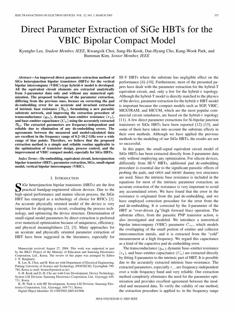
Fig. 1. Small-signal equivalent circuit model for a modern deep-trenchisolated double-poly SiGe HBT in the forward active region.
Fig. 2. Layouts of the structures of a DUT, an OPEN dummy, and a SHORTdummy.
0.2–10.2 GHz, a m SiGe HBT fabricated by a0.35- m SiGe BiCMOS process technology at Samsung Elec-tronics Corporation, Ltd. The measured and simulated data havevery good agreements over the frequency range in a wide rangeof bias points. Therefore, the proposed extraction procedurecan be a useful method applicable to optimization of transistordesign, process control, and improvement of VBIC compactmodel, especially, for SiGe HBTs.
II. PAD DE-EMBEDDING AND EXTRACTION OF
EXTRINSIC ELEMENTS
Small-signal equivalent circuit model for a moderndeep-trench isolated double-poly SiGe HBT in the forwardactive region is shown in Fig. 1. The model is based on thewell-known hybrid- equivalent circuit which is a linearizedversion of the VBIC compact model [16]. We divide this circuitinto two parts, the inner part (in the dashed box) containingthe bias-dependent intrinsic elements, and the outer part withthe mostly bias-independent extrinsic elements. Non-VBICelement is introduced in order to model the capacitanceof the small overlapping area of the emitter and collectorinterconnection metals.
To extract the parameters, we have performed pad de-embed-ding with the industry-standard OPEN-SHORT method [17], [18]using two additional dummy structures shown in Fig. 2. Sincesome residual parasitics from the imperfect de-embedding al-ways remain, the de-embedding error is corrected by the S-pa-rameter measured at “over-driven ” operation. The next stepis an accurate extraction of extrinsic element values. Some of
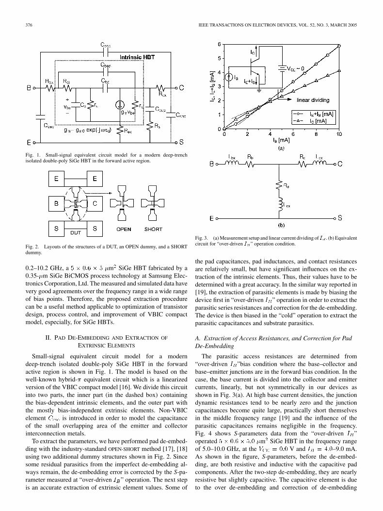
Fig. 3. (a) Measurement setup and linear current dividing of I . (b) Equivalentcircuit for “over-driven I ” operation condition.
the pad capacitances, pad inductances, and contact resistancesare relatively small, but have significant influences on the ex-traction of the intrinsic elements. Thus, their values have to bedetermined with a great accuracy. In the similar way reported in[19], the extraction of parasitic elements is made by biasing thedevice first in “over-driven ” operation in order to extract theparasitic series resistances and correction for the de-embedding.The device is then biased in the “cold” operation to extract theparasitic capacitances and substrate parasitics.
A. Extraction of Access Resistances, and Correction for PadDe-Embedding
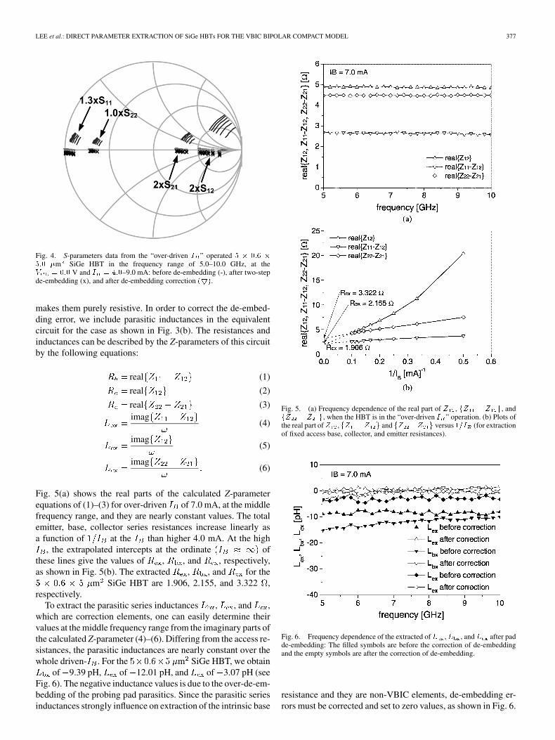
The parasitic access resistances are determined from“over-driven ”bias condition where the base–collector andbase–emitter junctions are in the forward bias condition. In thecase, the base current is divided into the collector and emittercurrents, linearly, but not symmetrically in our devices asshown in Fig. 3(a). At high base current densities, the junctiondynamic resistances tend to be nearly zero and the junctioncapacitances become quite large, practically short themselvesin the middle frequency range [19] and the influence of theparasitic capacitances remains negligible in the frequency.Fig. 4 shows S-parameters data from the “over-driven ”operated m SiGe HBT in the frequency rangeof 5.0–10.0 GHz, at the V and –9.0 mA.As shown in the figure, S-parameters, before the de-embed-ding, are both resistive and inductive with the capacitive padcomponents. After the two-step de-embedding, they are nearlyresistive but slightly capacitive. The capacitive element is dueto the over de-embedding and correction of de-embedding
LEE et al.: DIRECT PARAMETER EXTRACTION OF SiGe HBTs FOR THE VBIC BIPOLAR COMPACT MODEL 377
Fig. 4. S-parameters data from the “over-driven I ” operated 5 � 0:6 �5:0 �m SiGe HBT in the frequency range of 5.0–10.0 GHz, at theV = 0:0 V and I = 4:0–9.0 mA: before de-embedding (-), after two-stepde-embedding (x), and after de-embedding correction (5).
makes them purely resistive. In order to correct the de-embed-ding error, we include parasitic inductances in the equivalentcircuit for the case as shown in Fig. 3(b). The resistances andinductances can be described by the Z-parameters of this circuitby the following equations:
real (1)
real (2)
real (3)imag
(4)
imag(5)
imag(6)
Fig. 5(a) shows the real parts of the calculated Z-parameterequations of (1)–(3) for over-driven of 7.0 mA, at the middlefrequency range, and they are nearly constant values. The totalemitter, base, collector series resistances increase linearly asa function of at the than higher 4.0 mA. At the high
, the extrapolated intercepts at the ordinate ofthese lines give the values of , , and , respectively,as shown in Fig. 5(b). The extracted , , and for the
m SiGe HBT are 1.906, 2.155, and 3.322 ,respectively.
To extract the parasitic series inductances , , and ,which are correction elements, one can easily determine theirvalues at the middle frequency range from the imaginary parts ofthe calculated Z-parameter (4)–(6). Differing from the access re-sistances, the parasitic inductances are nearly constant over thewhole driven- . For the m SiGe HBT, we obtain
of 9.39 pH, of 12.01 pH, and of 3.07 pH (seeFig. 6). The negative inductance values is due to the over-de-em-bedding of the probing pad parasitics. Since the parasitic seriesinductances strongly influence on extraction of the intrinsic base
Fig. 5. (a) Frequency dependence of the real part of Z , fZ � Z g, andfZ �Z g, when the HBT is in the “over-driven I ” operation. (b) Plots ofthe real part ofZ , fZ �Z g and fZ �Z g versus 1=I (for extractionof fixed access base, collector, and emitter resistances).
Fig. 6. Frequency dependence of the extracted ofL , L , and L after padde-embedding: The filled symbols are before the correction of de-embeddingand the empty symbols are after the correction of de-embedding.
resistance and they are non-VBIC elements, de-embedding er-rors must be corrected and set to zero values, as shown in Fig. 6.
378 IEEE TRANSACTIONS ON ELECTRON DEVICES, VOL. 52, NO. 3, MARCH 2005
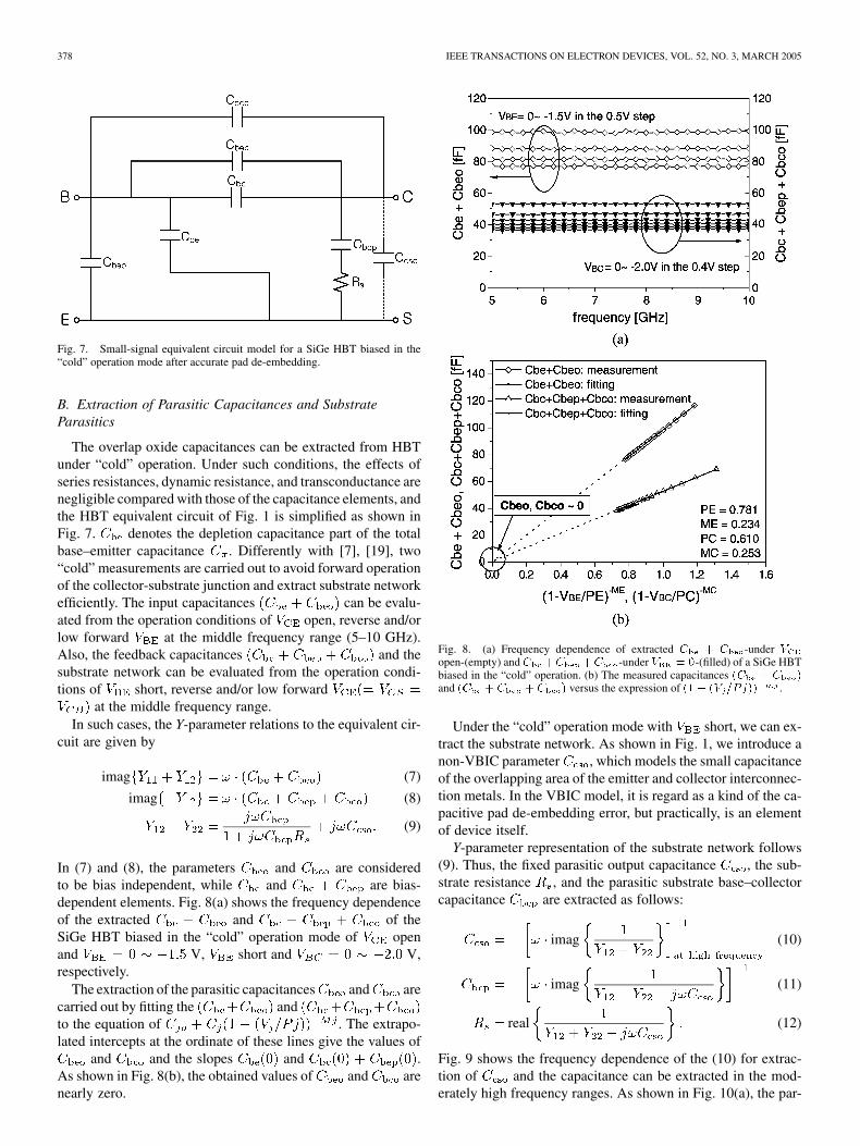
Fig. 7. Small-signal equivalent circuit model for a SiGe HBT biased in the“cold” operation mode after accurate pad de-embedding.
B. Extraction of Parasitic Capacitances and SubstrateParasitics
The overlap oxide capacitances can be extracted from HBTunder “cold” operation. Under such conditions, the effects ofseries resistances, dynamic resistance, and transconductance arenegligible compared with those of the capacitance elements, andthe HBT equivalent circuit of Fig. 1 is simplified as shown inFig. 7. denotes the depletion capacitance part of the totalbase–emitter capacitance . Differently with [7], [19], two“cold” measurements are carried out to avoid forward operationof the collector-substrate junction and extract substrate networkefficiently. The input capacitances can be evalu-ated from the operation conditions of open, reverse and/orlow forward at the middle frequency range (5–10 GHz).Also, the feedback capacitances and thesubstrate network can be evaluated from the operation condi-tions of short, reverse and/or low forward
at the middle frequency range.In such cases, the Y-parameter relations to the equivalent cir-
cuit are given by
imag (7)
imag (8)
(9)
In (7) and (8), the parameters and are consideredto be bias independent, while and are bias-dependent elements. Fig. 8(a) shows the frequency dependenceof the extracted and of theSiGe HBT biased in the “cold” operation mode of openand V, short and V,respectively.
The extraction of the parasitic capacitances and arecarried out by fitting the andto the equation of . The extrapo-lated intercepts at the ordinate of these lines give the values of
and and the slopes and .As shown in Fig. 8(b), the obtained values of and arenearly zero.
Fig. 8. (a) Frequency dependence of extracted C + C -under Vopen-(empty) and C +C +C -under V = 0-(filled) of a SiGe HBTbiased in the “cold” operation. (b) The measured capacitances (C + C )and (C +C + C ) versus the expression of (1� (V =Pj)) .
Under the “cold” operation mode with short, we can ex-tract the substrate network. As shown in Fig. 1, we introduce anon-VBIC parameter , which models the small capacitanceof the overlapping area of the emitter and collector interconnec-tion metals. In the VBIC model, it is regard as a kind of the ca-pacitive pad de-embedding error, but practically, is an elementof device itself.
Y-parameter representation of the substrate network follows(9). Thus, the fixed parasitic output capacitance , the sub-strate resistance , and the parasitic substrate base–collectorcapacitance are extracted as follows:
imag (10)
imag (11)
real (12)
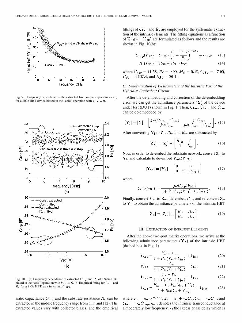
Fig. 9 shows the frequency dependence of the (10) for extrac-tion of and the capacitance can be extracted in the mod-erately high frequency ranges. As shown in Fig. 10(a), the par-
LEE et al.: DIRECT PARAMETER EXTRACTION OF SiGe HBTs FOR THE VBIC BIPOLAR COMPACT MODEL 379
Fig. 9. Frequency dependence of the extracted fixed output capacitance Cfor a SiGe HBT device biased in the “cold” operation with V = 0.
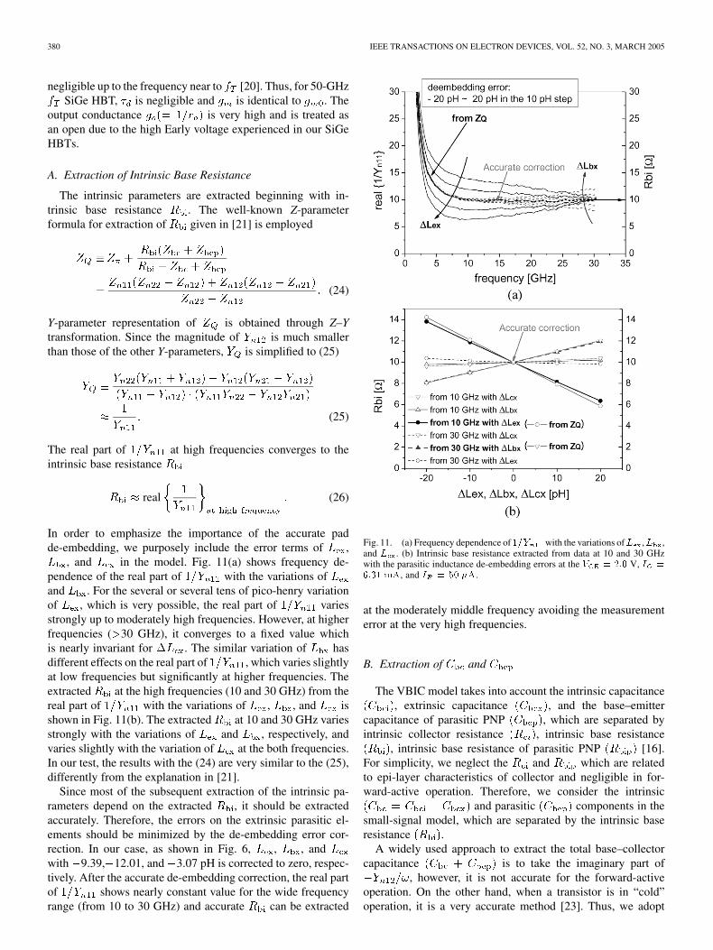
Fig. 10. (a) Frequency dependence of extracted C and R of a SiGe HBTbiased in the “cold” operation with V = 0. (b) Empirical fitting forC andR for a SiGe HBT, as a function of V .
asitic capacitance and the substrate resistance can beextracted in the middle frequency range from (11) and (12). Theextracted values vary with collector biases, and the empirical
fittings of and are employed for the systematic extrac-tion of the intrinsic elements. The fitting equations as a functionof are formulated as follows and the results areshown in Fig. 10(b):
(13)
(14)
where , , , ,, and .
C. Determination of Y-Parameters of the Intrinsic Part of theHybrid- Equivalent Circuit
After the de-embedding and correction of the de-embeddingerror, we can get the admittance parameters of the deviceunder test (DUT) shown in Fig. 1. Then, , , andcan be de-embedded by
(15)
After converting to , and are subtracted by
(16)
Now, in order to de-embed the substrate network, convert toand calculate to de-embed .
(17)
where
(18)
Finally, convert to , de-embed , and re-convertto to obtain the admittance parameters of the intrinsic HBT
(19)
III. EXTRACTION OF INTRINSIC ELEMENTS
After the above two-port matrix operations, we arrive at thefollowing admittance parameters of the intrinsic HBT(dashed box in Fig. 1)
(20)
(21)
(22)
(23)
where , , , and. denotes the intrinsic transconductance at
a moderately low frequency, the excess phase delay which is
380 IEEE TRANSACTIONS ON ELECTRON DEVICES, VOL. 52, NO. 3, MARCH 2005
negligible up to the frequency near to [20]. Thus, for 50-GHzSiGe HBT, is negligible and is identical to . The
output conductance is very high and is treated asan open due to the high Early voltage experienced in our SiGeHBTs.
A. Extraction of Intrinsic Base Resistance
The intrinsic parameters are extracted beginning with in-trinsic base resistance . The well-known Z-parameterformula for extraction of given in [21] is employed
(24)
Y-parameter representation of is obtained through Z–Ytransformation. Since the magnitude of is much smallerthan those of the other Y-parameters, is simplified to (25)
(25)
The real part of at high frequencies converges to theintrinsic base resistance
real (26)
In order to emphasize the importance of the accurate padde-embedding, we purposely include the error terms of ,
, and in the model. Fig. 11(a) shows frequency de-pendence of the real part of with the variations ofand . For the several or several tens of pico-henry variationof , which is very possible, the real part of variesstrongly up to moderately high frequencies. However, at higherfrequencies ( 30 GHz), it converges to a fixed value whichis nearly invariant for . The similar variation of hasdifferent effects on the real part of , which varies slightlyat low frequencies but significantly at higher frequencies. Theextracted at the high frequencies (10 and 30 GHz) from thereal part of with the variations of , , and isshown in Fig. 11(b). The extracted at 10 and 30 GHz variesstrongly with the variations of and , respectively, andvaries slightly with the variation of at the both frequencies.In our test, the results with the (24) are very similar to the (25),differently from the explanation in [21].
Since most of the subsequent extraction of the intrinsic pa-rameters depend on the extracted , it should be extractedaccurately. Therefore, the errors on the extrinsic parasitic el-ements should be minimized by the de-embedding error cor-rection. In our case, as shown in Fig. 6, , , andwith 9.39, 12.01, and 3.07 pH is corrected to zero, respec-tively. After the accurate de-embedding correction, the real partof shows nearly constant value for the wide frequencyrange (from 10 to 30 GHz) and accurate can be extracted
Fig. 11. (a) Frequency dependence of 1=Y with the variations ofL ,L ,and L . (b) Intrinsic base resistance extracted from data at 10 and 30 GHzwith the parasitic inductance de-embedding errors at the V = 2:0 V, I =
6:31 mA, and I = 50 �A.
at the moderately middle frequency avoiding the measurementerror at the very high frequencies.
B. Extraction of and
The VBIC model takes into account the intrinsic capacitance, extrinsic capacitance , and the base–emitter
capacitance of parasitic PNP , which are separated byintrinsic collector resistance , intrinsic base resistance
, intrinsic base resistance of parasitic PNP [16].For simplicity, we neglect the and which are relatedto epi-layer characteristics of collector and negligible in for-ward-active operation. Therefore, we consider the intrinsic
and parasitic components in thesmall-signal model, which are separated by the intrinsic baseresistance .
A widely used approach to extract the total base–collectorcapacitance is to take the imaginary part of
, however, it is not accurate for the forward-activeoperation. On the other hand, when a transistor is in “cold”operation, it is a very accurate method [23]. Thus, we adopt
LEE et al.: DIRECT PARAMETER EXTRACTION OF SiGe HBTs FOR THE VBIC BIPOLAR COMPACT MODEL 381
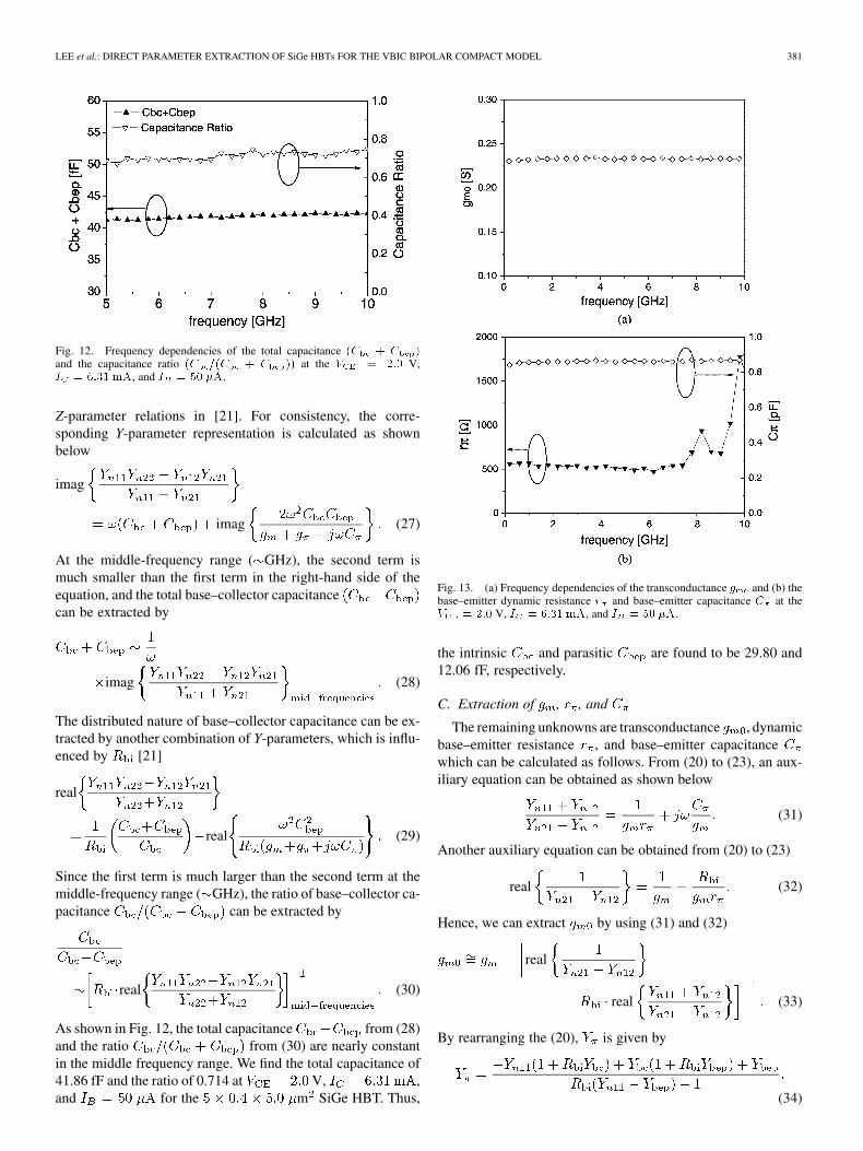
Fig. 12. Frequency dependencies of the total capacitance (C + C )and the capacitance ratio (C =(C + C )) at the V = 2:0 V,I = 6:31 mA, and I = 50 �A.
Z-parameter relations in [21]. For consistency, the corre-sponding Y-parameter representation is calculated as shownbelow
imag
imag (27)
At the middle-frequency range ( GHz), the second term ismuch smaller than the first term in the right-hand side of theequation, and the total base–collector capacitancecan be extracted by
imag (28)
The distributed nature of base–collector capacitance can be ex-tracted by another combination of Y-parameters, which is influ-enced by [21]
real
real (29)
Since the first term is much larger than the second term at themiddle-frequency range ( GHz), the ratio of base–collector ca-pacitance can be extracted by
real (30)
As shown in Fig. 12, the total capacitance from (28)and the ratio from (30) are nearly constantin the middle frequency range. We find the total capacitance of41.86 fF and the ratio of 0.714 at V, ,and for the m SiGe HBT. Thus,
Fig. 13. (a) Frequency dependencies of the transconductance g and (b) thebase–emitter dynamic resistance r and base–emitter capacitance C at theV = 2:0 V, I = 6:31 mA, and I = 50 �A.
the intrinsic and parasitic are found to be 29.80 and12.06 fF, respectively.
C. Extraction of , , and
The remaining unknowns are transconductance , dynamicbase–emitter resistance , and base–emitter capacitancewhich can be calculated as follows. From (20) to (23), an aux-iliary equation can be obtained as shown below
(31)
Another auxiliary equation can be obtained from (20) to (23)
real (32)
Hence, we can extract by using (31) and (32)
real
real (33)
By rearranging the (20), is given by
(34)
382 IEEE TRANSACTIONS ON ELECTRON DEVICES, VOL. 52, NO. 3, MARCH 2005
The and can be extracted from (34) using the intrinsicbase resistance and base–collector capacitances ( and
)
real(35)
imag (36)
The above extraction method for , , and rely on theintrinsic Y-parameter and intrinsic base resistance .Since we have developed very accurate extraction procedure forthose parameters, it is expected that the accuracies of the ex-tracted three values are high. Fig. 13 shows the extracted re-sults for m SiGe HBT at V,
, and . The extracted , , andare found to be 233 mS, 541 , and 0.86 pF, respectively.
IV. EXPERIMENTAL VERIFICATION AND DISCUSSION
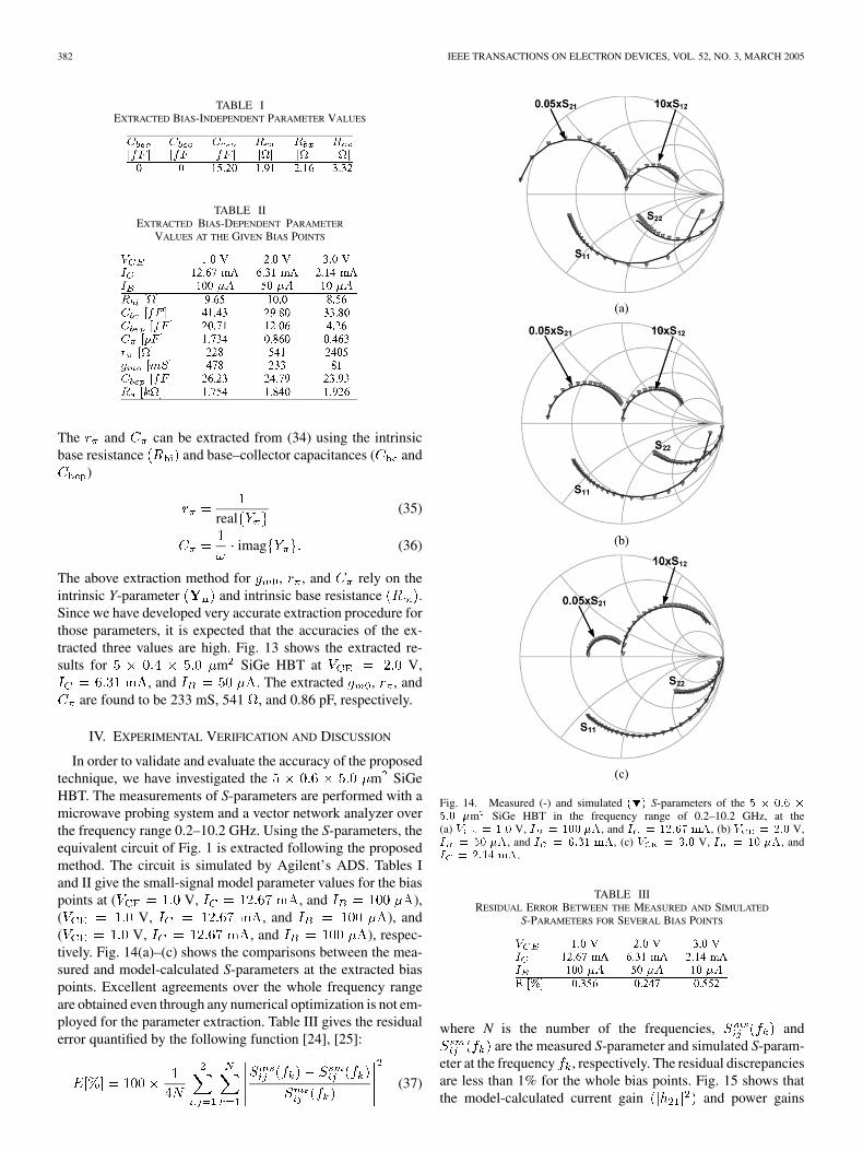
In order to validate and evaluate the accuracy of the proposedtechnique, we have investigated the m SiGeHBT. The measurements of S-parameters are performed with amicrowave probing system and a vector network analyzer overthe frequency range 0.2–10.2 GHz. Using the S-parameters, theequivalent circuit of Fig. 1 is extracted following the proposedmethod. The circuit is simulated by Agilent’s ADS. Tables Iand II give the small-signal model parameter values for the biaspoints at ( V, , and ),( V, , and ), and( V, , and ), respec-tively. Fig. 14(a)–(c) shows the comparisons between the mea-sured and model-calculated S-parameters at the extracted biaspoints. Excellent agreements over the whole frequency rangeare obtained even through any numerical optimization is not em-ployed for the parameter extraction. Table III gives the residualerror quantified by the following function [24], [25]:
(37)
Fig. 14. Measured (-) and simulated ( ) S-parameters of the 5 � 0:6 �5:0 �m SiGe HBT in the frequency range of 0.2–10.2 GHz, at the(a) V = 1:0 V, I = 100 �A, and I = 12:67 mA, (b) V = 2:0 V,I = 50 �A, and I = 6:31 mA, (c) V = 3:0 V, I = 10 �A, andI = 2:14 mA.
TABLE IIIRESIDUAL ERROR BETWEEN THE MEASURED AND SIMULATED
S-PARAMETERS FOR SEVERAL BIAS POINTS
where N is the number of the frequencies, andare the measured S-parameter and simulated S-param-
eter at the frequency , respectively. The residual discrepanciesare less than 1% for the whole bias points. Fig. 15 shows thatthe model-calculated current gain and power gains
LEE et al.: DIRECT PARAMETER EXTRACTION OF SiGe HBTs FOR THE VBIC BIPOLAR COMPACT MODEL 383
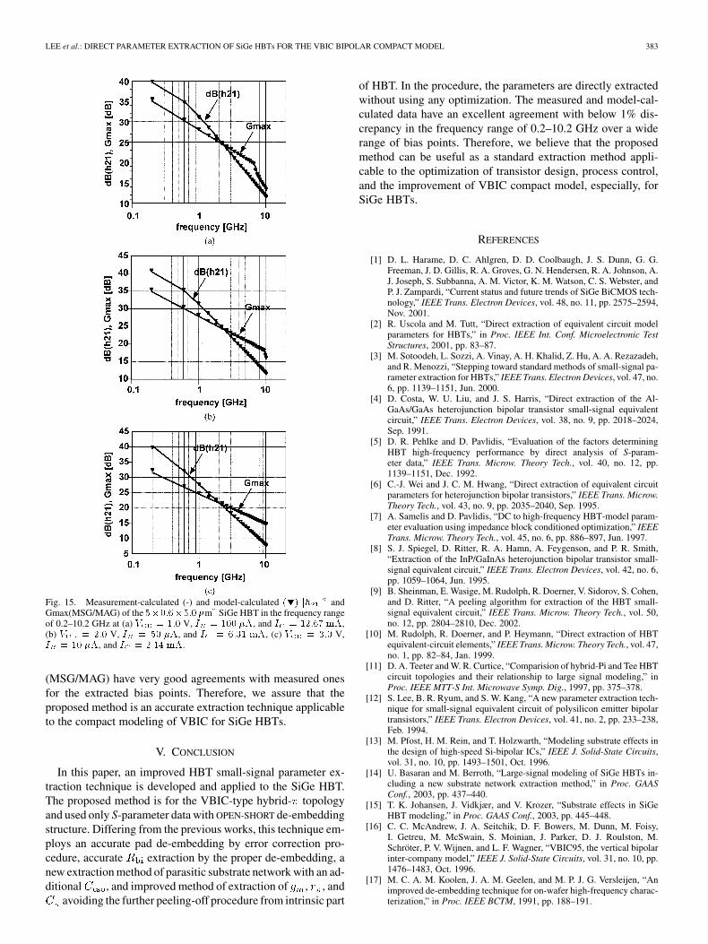
Fig. 15. Measurement-calculated (-) and model-calculated ( ) jh j andGmax(MSG/MAG) of the 5�0:6�5:0�m SiGe HBT in the frequency rangeof 0.2–10.2 GHz at (a) V = 1:0 V, I = 100 �A, and I = 12:67 mA,(b) V = 2:0 V, I = 50 �A, and I = 6:31 mA, (c) V = 3:0 V,I = 10 �A, and I = 2:14 mA.
(MSG/MAG) have very good agreements with measured onesfor the extracted bias points. Therefore, we assure that theproposed method is an accurate extraction technique applicableto the compact modeling of VBIC for SiGe HBTs.
V. CONCLUSION
In this paper, an improved HBT small-signal parameter ex-traction technique is developed and applied to the SiGe HBT.The proposed method is for the VBIC-type hybrid- topologyand used only S-parameter data with OPEN-SHORT de-embeddingstructure. Differing from the previous works, this technique em-ploys an accurate pad de-embedding by error correction pro-cedure, accurate extraction by the proper de-embedding, anew extraction method of parasitic substrate network with an ad-ditional , and improved method of extraction of , , and
avoiding the further peeling-off procedure from intrinsic part
of HBT. In the procedure, the parameters are directly extractedwithout using any optimization. The measured and model-cal-culated data have an excellent agreement with below 1% dis-crepancy in the frequency range of 0.2–10.2 GHz over a widerange of bias points. Therefore, we believe that the proposedmethod can be useful as a standard extraction method appli-cable to the optimization of transistor design, process control,and the improvement of VBIC compact model, especially, forSiGe HBTs.
REFERENCES
[1] D. L. Harame, D. C. Ahlgren, D. D. Coolbaugh, J. S. Dunn, G. G.Freeman, J. D. Gillis, R. A. Groves, G. N. Hendersen, R. A. Johnson, A.J. Joseph, S. Subbanna, A. M. Victor, K. M. Watson, C. S. Webster, andP. J. Zampardi, “Current status and future trends of SiGe BiCMOS tech-nology,” IEEE Trans. Electron Devices, vol. 48, no. 11, pp. 2575–2594,Nov. 2001.
[2] R. Uscola and M. Tutt, “Direct extraction of equivalent circuit modelparameters for HBTs,” in Proc. IEEE Int. Conf. Microelectronic TestStructures, 2001, pp. 83–87.
[3] M. Sotoodeh, L. Sozzi, A. Vinay, A. H. Khalid, Z. Hu, A. A. Rezazadeh,and R. Menozzi, “Stepping toward standard methods of small-signal pa-rameter extraction for HBTs,” IEEE Trans. Electron Devices, vol. 47, no.6, pp. 1139–1151, Jun. 2000.
[4] D. Costa, W. U. Liu, and J. S. Harris, “Direct extraction of the Al-GaAs/GaAs heterojunction bipolar transistor small-signal equivalentcircuit,” IEEE Trans. Electron Devices, vol. 38, no. 9, pp. 2018–2024,Sep. 1991.
[5] D. R. Pehlke and D. Pavlidis, “Evaluation of the factors determiningHBT high-frequency performance by direct analysis of S-param-eter data,” IEEE Trans. Microw. Theory Tech., vol. 40, no. 12, pp.1139–1151, Dec. 1992.
[6] C.-J. Wei and J. C. M. Hwang, “Direct extraction of equivalent circuitparameters for heterojunction bipolar transistors,” IEEE Trans. Microw.Theory Tech., vol. 43, no. 9, pp. 2035–2040, Sep. 1995.
[7] A. Samelis and D. Pavlidis, “DC to high-frequency HBT-model param-eter evaluation using impedance block conditioned optimization,” IEEETrans. Microw. Theory Tech., vol. 45, no. 6, pp. 886–897, Jun. 1997.
[8] S. J. Spiegel, D. Ritter, R. A. Hamn, A. Feygenson, and P. R. Smith,“Extraction of the InP/GaInAs heterojunction bipolar transistor small-signal equivalent circuit,” IEEE Trans. Electron Devices, vol. 42, no. 6,pp. 1059–1064, Jun. 1995.
[9] B. Sheinman, E. Wasige, M. Rudolph, R. Doerner, V. Sidorov, S. Cohen,and D. Ritter, “A peeling algorithm for extraction of the HBT small-signal equivalent circuit,” IEEE Trans. Microw. Theory Tech., vol. 50,no. 12, pp. 2804–2810, Dec. 2002.
[10] M. Rudolph, R. Doerner, and P. Heymann, “Direct extraction of HBTequivalent-circuit elements,” IEEE Trans. Microw. Theory Tech., vol. 47,no. 1, pp. 82–84, Jan. 1999.
[11] D. A. Teeter and W. R. Curtice, “Comparision of hybrid-Pi and Tee HBTcircuit topologies and their relationship to large signal modeling,” inProc. IEEE MTT-S Int. Microwave Symp. Dig., 1997, pp. 375–378.
[12] S. Lee, B. R. Ryum, and S. W. Kang, “A new parameter extraction tech-nique for small-signal equivalent circuit of polysilicon emitter bipolartransistors,” IEEE Trans. Electron Devices, vol. 41, no. 2, pp. 233–238,Feb. 1994.
[13] M. Pfost, H. M. Rein, and T. Holzwarth, “Modeling substrate effects inthe design of high-speed Si-bipolar ICs,” IEEE J. Solid-State Circuits,vol. 31, no. 10, pp. 1493–1501, Oct. 1996.
[14] U. Basaran and M. Berroth, “Large-signal modeling of SiGe HBTs in-cluding a new substrate network extraction method,” in Proc. GAASConf., 2003, pp. 437–440.
[15] T. K. Johansen, J. Vidkjær, and V. Krozer, “Substrate effects in SiGeHBT modeling,” in Proc. GAAS Conf., 2003, pp. 445–448.
[16] C. C. McAndrew, J. A. Seitchik, D. F. Bowers, M. Dunn, M. Foisy,I. Getreu, M. McSwain, S. Moinian, J. Parker, D. J. Roulston, M.Schröter, P. V. Wijnen, and L. F. Wagner, “VBIC95, the vertical bipolarinter-company model,” IEEE J. Solid-State Circuits, vol. 31, no. 10, pp.1476–1483, Oct. 1996.
[17] M. C. A. M. Koolen, J. A. M. Geelen, and M. P. J. G. Versleijen, “Animproved de-embedding technique for on-wafer high-frequency charac-terization,” in Proc. IEEE BCTM, 1991, pp. 188–191.
384 IEEE TRANSACTIONS ON ELECTRON DEVICES, VOL. 52, NO. 3, MARCH 2005
[18] H. Cho and D. E. Burk, “A three-step method for the de-embedding ofhigh-frequency S-parameter measurements,” IEEE Trans. Electron De-vices, vol. 38, no. 6, pp. 1371–1375, Jun. 1991.
[19] Y. Govert, P. J. Tasker, and K. H. Bachem, “A physical, yet simple,small-signal equivalent circuit for the heterojunction bipolar transistor,”IEEE Trans. Microw. Theory Tech., vol. 45, no. 1, pp. 149–153, Jan.1997.
[20] J. S. Hamel, “An accurate quasistatic method for determining the ex-cess phase shift in the base region of bipolar transistors,” in Proc. IEEEBCTM, 1992, pp. 208–211.
[21] Y. Suh, E. Seok, J.-H. Shin, B. Kim, D. Heo, A. Raghavan, and J. Laskar,“Direct extraction method for internal equivalent circuit parameters ofthe HBT small-signal hybrid-� model,” in IEEE MTT-S Int. MicrowaveSymp. Dig., 2000, pp. 1401–1404.
[22] T.-S. Horng, J.-M. Wu, and H.-H. Huang, “An extrinsic-inductance inde-pendent approach for direct extraction of HBT intrinsic circuit parame-ters,” IEEE Trans. Microw. Theory Tech., vol. 49, no. 12, pp. 2300–2305,Dec. 2001.
[23] M. W. Dvorak and C. R. Bolognesi, “On the accuracy of direct extractionof the heterojunction-bipolar-transistor equivalent-circuit model param-eters C , C , and R ,” IEEE Trans. Microw. Theory Tech., vol. 51,no. 6, pp. 1640–1649, Jun. 2003.
[24] B. Li, S. Prasad, L.-W. Yang, and S. C. Wang, “A semianalytical pa-rameter-extraction procedure for HBT equivalent circuit,” IEEE Trans.Microw. Theory Tech., vol. 46, no. 10, pp. 1427–1435, Oct. 1998.
[25] S. Bousnina, P. Mandeville, A. B. Kouki, R. Surridge, and F. M. Ghan-nouchi, “Direct parameter-extraction method for HBT small-signalmodel,” IEEE Trans. Microw. Theory Tech., vol. 50, no. 2, pp. 529–536,Feb. 2002.
[26] I. E. Getreu, Modeling the Bipolar Transistor. New York: Elsevier,1978.
[27] P. Antognetti and G. Massobrio, Semiconductor Device Modeling WithSPICE. New York: McGraw-Hill, 1988.
Kyungho Lee (S’04) was born in Miryang, Korea,in 1975. He received the B.S. degree in electronicsand electrical engineering from Kyungpook NationalUniversity, Taegu, Korea, in 1999, and the M.S. de-gree in electronics and electrical engineering fromthe Pohang University of Science and Technology,Pohang, Korea, in 2001, where he is currently pur-suing the Ph.D. degree.
His research interests include device design andfabrication of high-speed InP-based HBTs and RFmodeling of SiGe HBTs and MOSFETs.
Kwangsik Choi was born in Pohang, Korea, in1977. He received the B.S. degree in electronics andelectrical engineering from Inha University, Inchon,Korea, in 2003, and is currently pursuing the M.S.degree from the Pohang University of Science andTechnology.
His research interests are the development of high-speed InP DHBTs and device physics.
Sang-Ho Kook received the B.S. and M.S. degrees inelectrical engineering from Korea University, Seoul,Korea, in 1998 and 2000, respectively.
In 2000, he joined the Core Development, DeviceTechnology, System LSI division, Samsung Elec-tronics Corporation, Ltd, Gyeonggi-Do, Korea. Hispresent research interest includes the modeling andparameter extraction of SiGe HBT, RF CMOS, andsub-90-nm devices.
Dae-Hyung Cho received the Ph.D. degree in elec-trical engineering from the University of Illinois atUrbana-Champaign in 1995.
From 1983 to 1990, he was with Samsung Elec-tronics Corporation, Ltd., Korea, where he workedon device modeling and circuit simulation. Until1995, he was a Research Assistant at the BeckmanInstitute for Advanced Science and Technology, Ur-bana, IL. In 1995, he joined the System IC Division,Hyundai Electronics Corporation, Korea, where hewas in charge of the device characterization group.
In 1997, he joined the TCAD Group, Intel Corporation, Santa Clara, CA, wherehe was Staff Engineer until 2002, where he worked on advanced noise andRF characterization and modeling. In 2002, he joined the Core Development,Device Technology, System LSI Division, Samsung Electronics Corporation,Ltd., Gyeonggi-Do, Korea, where he has been leading projects in the areas ofSiGe HBT, RF CMOS, sub-90-nm advanced device modeling, electrostaticdischarge (ESD), and IO designs.
Kang-Wook Park received the B.S. and M.S. de-grees in ceramic engineering from Yonsei University,Seoul, Korea, in 1989 and 1995, respectively.
From 1990 to 1995, he joined the process researchcenter of Samsung Electronics Corporation, Ltd,Gyeonggi-Do, Korea, and worked on high-speedbipolar and BiCMOS process development. In 1996,he moved to the RF Development, System LSIDivision. He joined the high-speed BiCMOS processdevelopment project and production projects. Heis currently in charge of the high-speed SiGe HBT
BiCMOS process development and mass production setup.
Bumman Kim (S’77–M’78–SM’97) receivedthe Ph.D. degree in electrical engineering fromCarnegie-Mellon University, Pittsburgh, PA, in1979.
From 1978 to 1981, he was engaged in fiber-opticnetwork component research with GTE Laboratories,Inc. In 1981, he joined the Central Research Labora-tories, Texas Instruments Incorporated, where he wasinvolved in development of GaAs power FETs andmonolithic microwave integrated circuits (MMICs).He has developed a large-signal model of a power
FET, dual-gate FETs for gain control, high-power distributed amplifiers, andvarious millimeter-wave MMICs. In 1989, he joined the Pohang University ofScience and Technology, Pohang, Korea, where he is a Professor in the Elec-tronic and Electrical Engineering Department, and Director of the MicrowaveApplication Research Center, where he is involved in device and circuit tech-nology for RFICs. He was a Visiting Professor of Electrical Engineering withthe California Institute of Technology, Pasadena, in 2001. He has authored over150 published technical papers.
Dr. Kim is a member of the Korean Academy of Science and Technology andthe Academy of Engineering of Korea. He is an Associate Editor for the IEEETRANSACTIONS ON MICROWAVE THEORY AND TECHNIQUES.