Directing Cluster Formation of Au Nanoparticles from ColloidalSolutionSarah M. Adams,† Salvatore Campione,‡ Filippo Capolino,‡ and Regina Ragan*,†
†Department of Chemical Engineering and Materials Science, University of California, Irvine, Irvine, California 92697, United States‡Department of Electrical Engineering and Computer Science, University of California, Irvine, Irvine, California 92697, United States
*S Supporting Information
ABSTRACT: Discrete clusters of closely spaced Au nanoparticles canbe utilized in devices from photovoltaics to molecular sensors because ofthe formation of strong local electromagnetic field enhancements whenilluminated near their plasmon resonance. In this study, scalable,chemical self-organization methods are shown to produce Au nano-particle clusters with uniform nanometer interparticle spacing. Theperformance of two different methods, namely electrophoresis anddiffusion, for driving the attachment of Au nanoparticles using achemical cross-linker on chemically patterned domains of polystyrene-block-poly(methyl methacrylate) (PS-b-PMMA) thin films are evaluated.Significantly, electrophoresis is found to produce similar surfacecoverage as diffusion in 1/6th of the processing time with an ∼2-fold increase in the number of Au nanoparticles formingclusters. Furthermore, average interparticle spacing within Au nanoparticle clusters was found to decrease from 2−7 nm fordiffusion deposition to approximately 1−2 nm for electrophoresis deposition, and the latter method exhibited better uniformitywith most clusters appearing to have about 1 nm spacing between nanoparticles. The advantage of such fabrication capability issupported by calculations of local electric field enhancements using electromagnetic full-wave simulations from which we canestimate surface-enhanced Raman scattering (SERS) enhancements. In particular, full-wave results show that the maximum SERSenhancement, as estimated here as the fourth power of the local electric field, increases by a factor of 100 when the gap goes from2 to 1 nm, reaching values as large as 1010, strengthening the usage of electrophoresis versus diffusion for the development ofmolecular sensors.
■ INTRODUCTION
It has long been established that local electromagnetic fieldenhancements observed in noble metal nanoparticles, as aresult of excitation at the plasmon resonance, increase asnanoparticles electromagnetically couple with nanometer scaleinterparticle spacing.1,2 Significant advances in controlling thenanostructure and local composition via chemical synthesis3−6
coupled with theoretical understanding of electromagneticcoupling2,7−12 allows for tuning optical properties across theelectromagnetic spectrum. While these plasmonic systems havebeen demonstrated to have numerous applications such asmolecular sensors and efficiency-enhanced photovoltaics,scalable methods to produce nanostructures over a large areaon surfaces using processes that are nonprohibitive in cost arestill challenging.Here, using chemical assembly, colloidal metal nanostruc-
tures are fabricated on substrates with nanometer scaleinterparticle spacing over sample areas of 1 cm2. This permitsthe versatility achievable in chemical synthesis to be utilized onsurfaces. Furthermore, chemical assembly relies on solutionmethods and avoids costly lithographic techniques fornanostructure formation on substrates while at the same timeachieving nanometer interparticle spacing, which is unachiev-able even with electron beam lithography.13 Assembly from
colloidal solution as performed here allows for attachment ofcomplex nanostructures, including core−shell and facetedstructures,14 to patterned chemical domains that can achievelarge area ordering when integrated with larger-scale litho-graphic methods such as with graphoepitaxial patterning15 orpatterning chemical domains using UV lithography.16 In thecase of diblock copolymers thin films, morphology is variableby altering the copolymer molecular weights,17,18 and orderedsurface patterns have been produced using field-assistedpatterning19 and solvent evaporation.20 Planar assemblies ofisolated Au nanoparticles and/or clusters can be used in anumber of applications, including highly sensitive molecularsensors based on SERS21−23 and increased efficiency inphotovoltaic devices.24,25 Inexpensive production of denseplanar assemblies of discrete clusters of nanoparticles wouldcontribute greatly to developing plasmonic devices.In this paper we compare two methods of directing
nanoparticle deposition in solution on PMMA domains ofpolystyrene-block-poly(methyl methacrylate) (PS-b-PMMA)thin films: diffusion and electrophoresis. Diffusion deposition
Received: January 2, 2013Revised: February 27, 2013Published: March 8, 2013
relies on random Brownian motion, whereas in electrophoreticdeposition (EPD) an external field directs charged nano-particles to an oppositely charged electrode. EPD haspreviously been used to direct colloidal nanoparticles onpatterned conductive regions on surfaces but not to produceisolated nanoparticle clusters. For example, methods to designpatterned nanoparticle arrays with EPD on conductive domainshave been patterned either on microscale domains,26 as isolatedsingle nanoparticles,27,28 or in linear domains.27,29 In this study,a PS-b-PMMA thin film on highly doped Si is used as theworking electrode. The film is not directly etched, but insteadPMMA domains are chemically modified for chemical attach-ment of a thioctic acid (TA)-functionalized nanoparticle fromcolloid.30 Previous studies of nanoparticle deposition with EPDhave demonstrated that dielectric polymer films coated onconductive electrodes can produce nanoparticle films withhomogeneous morphology of comparable quality to thosedeposited directly on conductive substrates.31,32 We useaqueous-based EPD, which benefits from faster kinetics,reduced requisite voltage, suitability for materials most stablein aqueous solutions, and environmental benefits whencompared to more common nonpolar solvents.33 We findthat EPD can produce comparable areal density of Aunanoparticles on PS-b-PMMA thin films in 1/6th of theprocessing time with respect to random diffusion. This issignificant because processing time relates directly to processingcosts. Importantly, we also find that EPD deposition leads toonly a small fraction, <20%, of isolated Au nanoparticles on thesurface, whereas diffusion has ∼50% isolated Au nanoparticles.Furthermore, when using EPD, Au clusters have relativelyuniform interparticle spacing that is approximately 1−2 nm. Wedemonstrate, using electromagnetic full-wave simulations, thatthese two latter EPD properties lead to a 100-fold increase inelectromagnetic field intensity as the interparticle spacing isdecreased from 4 to 1 nm that can lead to up to a 104 increasein SERS intensity. These field enhancements are thus criticalfor decreasing detection limits in molecular sensors.
■ RESULTS AND DISCUSSIONFirst, diffusion and electrophoresis were compared in terms ofAu nanoparticle coverage on the PMMA domains of PS-b-PMMA thin films. Figure 1a depicts how Au nanoparticles arechemically assembled on PS-b-PMMA thin films as described inprior work.30 Here we show Au nanoparticles that have beenfunctionalized with TA ligand molecules and PS-b-PMMA thinfilms that have been treated with ethylenediamine (ED) indimethyl sulfoxide (DMSO) solution are illustrated. 1-Ethyl-3-[3-(dimethylamino)propyl]carbodiimide hydrochloride (EDC)and N-hydroxysulfosuccinimide (S-NHS) (EDC/S-NHS)cross-linking chemistry is then used to couple Au nanoparticlesto chemically modified PMMA domains,30 since this chemistryhas been reported to induce the covalent attachment ofcarboxylic acid end groups with amine end groups.34 Inprevious work, we have observed negligible Au nanoparticleattachment when the chemical surface treatment and cross-linking steps were not performed.30 The diffusion depositionmethod is depicted in Figure 1b, where the PS-b-PMMAsample surface is suspended face down in the nanoparticlecolloidal solution and random Brownian motion leads tosurface−nanoparticle interactions. The EPD method isdepicted in Figure 1c, where the PS-b-PMMA thin film hasbeen deposited on highly doped Si, ρ = 0.001 ohm·cm, which isused as the working electrode. A Pt electrode is suspended in
the aqueous Au nanoparticle solution as the counter electrode.Zeta potential measurement of the TA-functionalized Aunanoparticles provides values of −52.8 ± 13.5 mV for 20 nmAu nanoparticles and −35.0 ± 5.4 mV for 10 nm Aunanoparticles, and thus the nanoparticles will be attracted tothe Si sample surface with the PS-b-PMMA thin film with thepositive applied bias. While this apparatus was designed todeposit nanoparticle clusters on a 1 cm2 substrate, the processcould theoretically be designed with larger apparatus toaccommodate larger conductive substrates provided the electricfield strength is maintained across the surface area of thesubstrate with a constant electrode distance.PS-b-PMMA thin films with different surface morphology
were used as templates for Au nanoparticle attachment. It iswell-known that molecular weight affects the surface morphol-ogy of diblock copolymer thin films.18,35 The molecular weightsof the copolymer precursor were varied to obtain cylindricaland lamellar PMMA domains. In Figure 2, 1 μm × 1 μm AFMtopography images of PS-b-PMMA thin films with (a) Mn of55-b-22 kg mol−1, referred to as b(20 nm), (b) Mn of 260-b-63.5 kg mol−1, referred to as b(40 nm), and (c) Mn of 170-b-145 kg mol−1, referred to as b(Lam). In Figures 2a and 2b, theobserved morphology is cylindrical. PMMA domains havemean diameter of 20 nm in Figure 2a, thus are referred to asb(20 nm), and mean diameter of 40 nm in Figure 2b, thusreferred to as b(40 nm). A lamellar-like configuration ofPMMA domains, referred to as b(Lam), is shown in Figure 2c.Phase contrast images are included as insets in the AFMtopography images of Figure 2 to clearly identify the PMMAdomains that appear darker when imaged in repulsive modeduring intermittent contact mode AFM imaging.36
To improve attachment of Au nanoparticles on PMMAdomains using the EPD method, first the applied voltage duringEPD was varied to maximize Au nanoparticle surface coverageusing this process. Figure 3 shows SEM images of 20 nm Au
Figure 1. Illustration of chemical self-assembly of Au nanoparticles onPS-b-PMMA thin films showing (a) schematic of TA-functionalizedAu nanoparticles with carboxylic acid end groups attached to ED-treated PMMA domains with amine end groups using EDC/S-NHS asa cross-linker. Schematics of assembly methods are shown for (b)diffusion deposition and (c) EPD.
nanoparticles deposited on b(40 nm) thin films using EPD for10 min at various applied voltages: (a) 1.0, (b) 1.2, (c) 1.5, and(d) 1.7 V with a 10 mm distance between the electrodes. Figure3e is a graph of the average Au nanoparticle surface coverage, interms of average number of nanoparticles per unit area, for eachapplied voltage as determined from ten different 9 μm2 regionson SEM images. Error bars represent the standard deviation inthe measurements. The Au nanoparticle surface coverageincreases with increased applied voltage up to 1.2 V and thendecreases with further increases in applied voltage. The
relationship between nanoparticle coverage and applied voltageobserved in Figure 3 is not unexpected since the electrolysis ofwater will occur at voltages above 1.23 V at acidic pH and T =25 °C based on the Nernst equation. Electrolysis will locallylower the pH near the working electrode.37 At low pH, EDC-activated carbodiimide attachment rates will decrease and EDCdecomposition will increase.34 Other electrochemical decom-position reactions38−40 may also occur at the electrodes.Typically reduced voltage,27,41,42 pulsed dc fields,37,42−44 andasymmetric ac fields44,45 have previously been found to inhibitelectrolysis. We find that voltages at or below 1.2 V appear toreduce the negative effects of water electrolysis since this yieldsthe maximum nanoparticle surface coverage.Diffusion deposition and EPD, with an applied voltage of 1.2
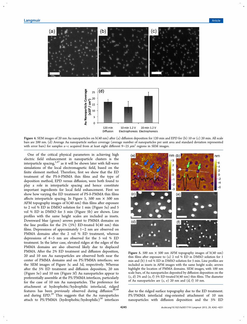
V, are directly compared for the deposition of 20 nm Aunanoparticles on b(40 nm) thin films. While increasedconcentration of EDC cross-linker was demonstrated in ourprevious work21 to increase nanoparticle coverage and clusterformation, analysis of Au nanoparticle attachment using EPDon b(40 nm) and b(Lam) in Figure S1 of the SupportingInformation demonstrated a maximum threshold of Aunanoparticle coverage without aggregation was reached afterthe addition of 38 μM EDC (94 μM S-NHS) and washenceforth used. In Figure 4, representative SEM images (1 μm× 1 μm) are provided of the surfaces following nanoparticledeposition by (a) diffusion for 120 min, (b) EPD for 10 min,and (c) EPD for 20 min. Larger scale 4 μm × 4 μm SEMimages of the same samples are provided in the Figure S2 forthe 120 min diffusion and 10 and 20 min EPD measurements.We found that without using a fresh solution no furtherincrease of nanoparticle coverage was observed after a 60 mindiffusion deposition or a 10 min EPD. The colloidalnanoparticle solutions were thus replaced with a freshly madesolution every 60 min for diffusion deposition and every 10 minfor EPD, since EDC has a high rate of hydrolysis during EPD.The t1/2 of EDC is 72 min at the buffered pH of 6.2, and thehydrolysis rate increases as pH decreases.46 Figure 4d is a graphof the average Au nanoparticle surface coverage for bothdiffusion deposition and EPD that was determined from SEMimages of at least eight different 9−25 μm2 regions. The data inFigure 4d demonstrate nanoparticle surface coverage increaseswith increased time for EPD, and after 20 min, EPD producesthe same Au nanoparticle surface coverage as a 120 mindiffusion process. On average, EPD produces surfaces with 28%nanoparticle coverage on PMMA domains with minimal largeaggregate formation on the surface. In comparison, increases incoverage using diffusion deposition were previously achieved byincreasing TA concentrations that led to some nanoparticleaggregate formation on the surface.21
Figure 2. AFM topography images of PS-b-PMMA thin films with (a) Mn of 55-b-22 kg mol−1, referred to as b(20 nm), (b) Mn of 260-b-63.5 kgmol−1, referred to as b(40 nm), and (c) Mn of 170-b-145 kg mol
−1, referred to as b(Lam). Phase contrast AFM images are shown as insets. All scalebars are 200 nm.
Figure 3. SEM images of 20 nm Au nanoparticles on b(40 nm) thinfilms after 10 min EPD at an applied voltage of (a) 1.0, (b) 1.2, (c) 1.5,and (d) 1.7 V. All scale bars are 500 nm. (e) Graph of Au nanoparticlesurface coverage (average number of nanoparticles per unit area andstandard deviation represented with error bars) as a function ofapplied EPD voltage.
One of the critical physical parameters in achieving highelectric field enhancement in nanoparticle clusters is theinterparticle spacing,1,47 as it will be shown later with full-wavesimulations of the local electromagnetic field, based on thefinite element method. Therefore, first we show that the EDtreatment of the PS-b-PMMA thin films and the type ofdeposition method, EPD versus diffusion, were both found toplay a role in interparticle spacing and hence constituteimportant ingredients for local field enhancement. First weshow how varying the ED treatment of PS-b-PMMA thin filmsaffects interparticle spacing. In Figure 5, 500 nm × 500 nmAFM topography images of b(40 nm) thin films after exposureto 2 vol % ED in DMSO solution for 1 min (Figure 5a) and 5vol % ED in DMSO for 5 min (Figure 5b) are shown. Lineprofiles with the same height scales are included as insets.Downward blue (green) arrows point to PMMA domains onthe line profiles for the 2% (5%) ED-treated b(40 nm) thinfilms. Depressions of approximately 1−2 nm are observed onPMMA domains after the 2 vol % ED treatment, whereasdepressions of 4−5 nm are observed for the 5 vol % EDtreatment. In the latter case, elevated ridges at the edges of thePMMA domains are also observed likely due to displacedPMMA. After the 2% ED treatment and diffusion deposition,20 and 10 nm Au nanoparticles are observed both near thecenter of PMMA domains and on PS/PMMA interfaces; seethe SEM images of Figure 5c and 5d, respectively. Whereasafter the 5% ED treatment and diffusion deposition, 20 nm(Figure 5e) and 10 nm (Figure 5f) Au nanoparticles appear topreferentially assemble at the PS/PMMA interfaces, particularlyfor the case of 10 nm Au nanoparticles. The preference forattachment at hydrophobic/hydrophilic interfacial, ridgedfeatures has been previously observed during diffusion48,49
and during EPD.29 This suggests that the Au nanoparticlesattach to PS/PMMA (hydrophobic/hydrophilic)30 interfaces
due to the ridged surface topography due to the ED treatment.PS/PMMA interfacial ring-oriented attachment of 10 nmnanoparticles with diffusion deposition and the 5% ED
Figure 4. SEM images of 20 nm Au nanoparticles on b(40 nm) after (a) diffusion deposition for 120 min and EPD for (b) 10 or (c) 20 min. All scalebars are 200 nm. (d) Average Au nanoparticle surface coverage (average number of nanoparticles per unit area and standard deviation representedwith error bars) for samples a−c acquired from at least eight different 9−25 μm2 regions in SEM images.
Figure 5. 500 nm × 500 nm AFM topography images of b(40 nm)thin films after exposure to (a) 2 vol % ED in DMSO solution for 1min and (b) 5 vol % ED in DMSO solution for 5 min. Line profiles areincluded as insets in AFM images with the same height scale; arrowshighlight the location of PMMA domains. SEM images, with 100 nmscale bars, of Au nanoparticles deposited by diffusion deposition on the(c, d) 2% and (e, f) 5% ED-treated b(40 nm) thin films. The diameterof Au nanoparticles are (c, e) 20 nm and (d, f) 10 nm.
treatment generally leads to increased interparticle spacing inclusters that is not desirable for hot spot creation but may beapplicable for Fano resonances or supporting magneticmodes.50,51
A 5% ED treatment typically leads to higher Au nanoparticlecoverage. Thus, diffusion deposition and EPD were thencompared in terms of Au nanoparticle cluster formation onb(40 nm) surfaces after 5% ED treatment. In Figure 6a, thegraph shows the percentage of Au nanoparticles that formmultiparticle clusters on b(40 nm) thin films (the remainderare isolated Au nanoparticles) for both deposition methods.The graph was generated from SEM images, and representativeimages are shown in Figure S2. When comparing diffusion andEPD, the latter nearly doubles the relative number of Aunanoparticles arranged in clusters on the surface. Note thatEPD on unpatterned ED-treated PMMA surfaces and SiO2/Sisurfaces did not lead to cluster formation (see Figure S3), andthus it is the combination of chemical patterning and EPD thatleads to cluster formation. Figure 6b,c provides a table ofapproximately 80 nm × 80 nm SEM images of representativeclusters on b(40) thin films observed after diffusion deposition(Figure 6b) and EPD (Figure 6c), and their frequency ofoccurrence is listed as text in the images. The first row of SEMimages corresponds to 20 nm Au nanoparticles and the secondrow corresponds to 10 nm Au nanoparticles. The first, second,third, and fourth columns correspond to single particles,dimers, trimers, and larger clusters having four or morenanoparticles, respectively.The percentage of Au nanoparticles incorporated in each
type of cluster that is listed on the SEM images of Figures 6band 6c was obtained from statistical analysis of 9 μm2 SEMimages collected at 4−8 different locations on each of thesample nanoparticle arrays. SEM analysis indicates that clusterformation during EPD has a different dynamic than duringdiffusion. EPD produces fewer single 20 nm Au nanoparticles,
26 ± 4%, than diffusion, which has 49 ± 4%. For both diffusiondeposition and EPD methods, the PMMA domain size/nanoparticle diameter ratio was found to influence the size ofthe cluster. Examination of the data in Figure 6 shows thatlarger clusters are observed more frequently on 40 nm PMMAdomains when the nanoparticle diameter was 10 nm, ratio 4/1,than when the diameter was 20 nm, ratio 2/1. Consider thatafter EPD deposition on b(40 nm) thin films single 10 nm Aunanoparticles on PMMA domains form with a probability of 14± 4% and 20 nm Au nanoparticles exist as single particles witha probability of 26 ± 4%. The number of isolated or single 10nm particles observed decreases by at least 10% for both EPDand diffusion deposition when compared to 20 nm nano-particles on b(40) thin films. Furthermore, when decreasing thePMMA domain size to 20 nm, the percentage of 10 nm Aunanoparticles in larger clusters, domain/diameter ratio of 2/1(see Figure S4) is similar to 20 nm nanoparticles on 40 nmPMMA having the same ratio. Overall, the PMMA domain tonanoparticle diameter ratio influences the cluster size duringdiffusion deposition; larger domains yield on average largerclusters when the nanoparticle diameter is fixed.An increase in dimers and trimers on the surface is important
since these types of clusters are associated with high electricfield enhancements as shown in simulations in our previousstudies.21 Furthermore, when using EPD, the averageinterparticle spacing in clusters decreased to approximately1−2 nm and is more uniform in comparison to diffusiondeposition when examining the SEM images of Figure 6.Examination of the same Figure 6 shows that the interparticlegap spacing for 20 nm Au nanoparticles in clusters was 2−7 nmon average with diffusion deposition. Uniformity of interparticlespacing with isolated nanoparticle clusters has been quitechallenging using self-assembly methods, generally requiringthe addition of a molecular cross-linker between the nano-particles.52 The reduced interparticle spacing observed after
Figure 6. (a) Percentage of Au nanoparticles observed in clusters on the surface of b(40 nm) thin films as a function of deposition parameters. SEMimages of Au nanoparticle clusters with diameter of 20 nm (top row) and 10 nm (bottom row) after (b) diffusion deposition and (c) EPD. Thefrequency of occurrence of nanopartices in each type of cluster is listed on the bottom of the SEM images.
EPD may be associated with intertwining of the ligand (forthioctic acid it is ∼1 nm in length).41 Derjaguin−Laudau−Verwey−Overbeck (DLVO) theory also predicts that thedouble layer thins near the electrode surface due to increased inionic strength;53 in this case van der Waals forces will also leadto smaller interparticle spacings.54,55 The decrease ininterparticle spacing with EPD is critically important for localelectric field enhancements that are expected to rapidly increasewith decreasing interparticle spacing as this value goes below 10nm.56
Using our previous setup,21 we performed full-wavesimulations employing the finite element method (highfrequency structure simulator, HFSS, by Ansys Inc.) in orderto investigate the effect of changing interparticle gap spacing onSERS enhancement. In Figure 7, calculated electric fieldenhancements for 1−4 nm gap spacings between nanoparticlesin representative cluster configurations observed in SEMimages of Figure 6 are shown. We consider dimers, lineartrimers, and linear quadrumers since these represent dominantnanoparticle configurations observed on fabricated samples.The electric field enhancement is here intended as |Ecl/E0|,where E0 is the plane wave field without clusters (stillaccounting for the multilayered environment in simulations asdiscussed next) and Ecl is the field with clusters, occurringbetween the nanoparticles in the middle of the gap betweencontiguous nanoparticles. Therefore, we investigate the fieldenhancement in the “hot spots”. Moreover, Au nanoparticleshave diameter of ≈20 nm with permittivity taken from ref 57and have been assumed to be embedded in a layer withdielectric constant of 2.47 (40 nm thickness) on top of a siliconsubstrate. This dielectric permittivity of 2.47 is close in value tothe one of PMMA and a layer of benzenethiol moleculescovering the nanoparticles (in the simulations the nanoparticlesare assumed to be at the center of the 40 nm thick layer). Forsimplicity of calculations we array the clusters in a square
lattice, with a period large enough to affect weakly themaximum field between the nanoparticles in a cluster (seeSupporting Information in ref 21) so as the clusters can beconsidered isolated. We illuminate each cluster configurationwith a plane wave, with incidence orthogonal to the surface,with electric field polarized along the axis of the linear cluster,for the range of excitation wavelengths between 400 and 1000nm. Results in Figure 7 show that a slight increase in the gapsize dramatically diminishes the local electric field enhance-ment, going for example from about ≈365 for the linearquadrumer case with 1 nm gap to about ≈130 when the gap is2 nm to values less than ≈45 when the gap is 4 nm. We notealso the resonance blue shift for increasing gap size. Calculationof the local electric field enhancement allows us to infer anestimate of the theoretical SERS enhancement, simplycomputed here as the fourth power of the field enhancement|Ecl/E0|
4, which would range from about ≈1010 for the linearquadrumer case with 1 nm gap to about ≈3 × 10⁸ when the gapis 2 nm and finally to values less than ≈4 × 10⁶ when the gap is4 nm. This shows the potential of substrates made of linear andtriangular clusters of closely spaced nanoparticles for SERSapplications. Since EDP enables a higher fraction of clusterswith smaller gap size, it is expected that this method will lead toimproved performance for sensing applications.Polymer surface morphology was varied to examine the
effects on Au nanoparticle assembly. Au nanoparticle attach-ment on b(Lam), which has 48% PMMA surface area wascompared to that on b(40 nm), which has 20% PMMA surfacearea. Analysis of the SEM images, shown in Figure S1,demonstrates that Au surface coverage is ∼10% higher onb(Lam) surfaces. Figure 8a summarizes SEM data analyses andshows the percentage of nanoparticle assemblies in each of thelisted clusters. Note the increased number of dimer and lineartrimer cluster arrangements with b(Lam) when compared withb(40 nm). Using the same setup described to compute the
Figure 7. Theoretical electric field enhancement |Ecl/E0| computed in dimers, linear trimers, and linear quadrumers versus illumination wavelengthwhen excited with a plane wave orthogonal to the surface, with electric field polarized along the cluster axis. Results retrieved via full-wavesimulations employing the finite element method for various gap sizes.
Figure 8. (a) Percentage of Au nanoparticles observed in single particle clusters, dimers, linear trimers, 90° trimers, 60° trimers, and larger clusterson b(40 nm) and b(Lam) thin films using EPD acquired from SEM data. (b, c) Electric field enhancement for the two polarizations of the incidentplane wave in the insets for various cluster configurations: dimers, linear trimers, trimers 60°, trimers 90°, and linear quadrumers, for a gap of 1 nmbetween nanoparticles. The linear configurations are not reported in (c) because the wave is not expected to couple for plane wave polarizationorthogonal to the cluster axis.
results shown in Figure 7, we report in Figure 8b,c full-waveelectromagnetic results showing the theoretical electric fieldenhancement |Ecl/E0| for different cluster configurations. In thecase of triangular trimers, SEM images show that nanoparticlesmay be clustered with various angular values. That is why weanalyze here two representative cases of 60° and 90° angles.Interparticle gap size is kept equal to 1 nm, as in the previouscase for linear clusters, as well of the triangular clusters nowconsidered. We illuminate each structure with a plane wave,with incidence orthogonal to the surface, with electric fieldpolarized along the two directions in Figure 8b,c for the rangeof excitation wavelengths between 400 and 1000 nm. Results inFigure 8b,c show that stronger electric field enhancement isachieved with linear clusters (dimers, trimers, quadrumers)around 650 nm with respect to other trimer (triangular)configurations. We observe both increasing electric fieldenhancement and a resonance red shift for increasing numberof particles in the linear configurations. We also note thatelectric field enhancement values, relative to the gap distanceshere considered, are not very sensitive to the angular value intriangular trimers. Furthermore, for these clusters, onepolarization of the incident plane wave leads to slightlystronger electric field enhancement with respect to the other.These simulations overall show that the increased number ofdimers and trimers arrangements is important for use in sensingapplications. Linear trimers and quadrumers provide strongerelectric field enhancement than triangular clusters, when thepolarization matches with the axis of the linear cluster. Viceversa, triangular clusters provide slightly weaker fields thanlinear trimers and quadrumers, but their field enhancement, andthus SERS, is robust with respect to the polarization. Indeed,we estimate SERS enhancements of about 109−1010 whencomputed as the fourth power of the field enhancement. As aconsequence of such numerical results, we estimate that EPDattachment on b(Lam) PS-b-PMMA array provides a SERSsurface that produces stronger signal enhancements ascompared to b(40 nm) due to the combination of bothincreased total nanoparticle attachment and increased fre-quency of nanoparticle clustering in such configurations.
■ CONCLUSIONSIn this study, we compare EPD to diffusion deposition forassembly of Au nanoparticle clusters on PMMA domains of PS-b-PMMA thin films. We find that EPD, when adjusting dcvoltage to reduce electrolysis, requires only 1/6th theprocessing time as diffusion for achieving comparable Aunanoparticle surface coverage, >1010 nanoparticles/cm2. EPDleads to more Au nanoparticles forming clusters on the surfaceversus diffusion assembly for both 10 and 20 nm diameternanoparticles. The plasmon resonance of 20 nm Au nano-particles, as determined from full wave simulations, occurs nearthe wavelength of a helium−neon laser (633 nm) and thus canbe excited with a standard laser. Optimization of the EPDprocess using an ac field,44,45 for example, could be used toincrease Au coverage in future work while still keeping thecoverage below the hexagonally close packed limit whereelectric field enhancements decrease.21 Moreover, EPDdemonstrated more uniformity of the interparticle spacingwithin nanoparticle clusters, with average spacing of 1−2 nmfor EPD in comparison to 2−7 nm for diffusion deposition.The decreased interparticle spacing within clusters is importantfor achieving increased electric field enhancements asdemonstrated by electromagnetic full-wave simulations. Simu-
lations demonstrated that dimer, linear trimer, and linearquadrumer nanoparticle clusters produced the strongestenhancements when comparing enhancements in isolatedclusters considered here. When the interparticle spacing inthe clusters is reduced to 1 nm, we estimate an increase in thelocal electric field enhancement. When estimating a theoreticalSERS enhancement (defined as the fourth power of the electricfield enhancement in the hot spots), we find the SERSenhancement can reach values as large as 1010 for the linearcluster configurations. In the case of triangular trimerconfigurations, we estimate slightly lower field enhancementsthan linear clusters; the theoretical SERS enhancements isestimated to reach ∼109 when the interparticle spacing is 1 nm,and SERS is not expected to be strongly dependent on thepolarization. PS-b-PMMA surface morphology affected clusterformation; on lamellar-like surface morphologies, b(Lam), weobserve an increased frequency of the more strongly fieldenhancing dimers and linear trimers in SEM images ascompared to cylindrical PMMA configurations, b(40 nm).Because of the higher coverage of PMMA domains on b(Lam)versus b(40 nm), we also obtain a higher overall coverage of Aunanoparticles on the surface. Optimization of b(Lam) surfacesin terms of uniformity of PMMA domains and EPD depositionparameters would be a good starting point for optimizingsensor performance. Overall, EPD produces a distribution ofclusters on the surface that include a high coverage of dimers,trimers, and quadrumers with nanometer interparticle gapspacings that are calculated to exhibit high electric fieldenhancements. EPD thus represents a low-cost method that ishighly desirable for the development of molecular scale sensors.
■ MATERIALS AND METHODSMaterials. The random copolymer poly(styrene-co-methyl meth-
acrylate)-α-hydroxyl-ω-tempo moiety (PS-r-PMMA) (Mn = 7400,59.6% PS) and block copolymer poly(styrene-b-methyl methacrylate)(PS-b-PMMA) (of molecular weights b(20 nm) Mn = 55-b-22 kgmol−1, b(40 nm) Mn = 260-b-63.5 kg mol−1, and b(Lam) Mn = 170-b-144 kg mol−1) were purchased from Polymer Source, Inc. (Dorval,Canada). Boron-doped silicon wafers with of resistivity 1−10 ohm·cmfor diffusion deposition were purchased from University Wafer (SouthBoston, MA), and Si wafers with resistivity of 0.001−0.004 ohm·cmfor electrophoresis deposition (EPD) were purchased from VirginiaSemiconductor (Frederickburg, VA). Gold(III) chloride trihydrate(HAuCl4·3H2O), DL-6,8-thioctic acid (C8H14O2S1) (TA), ethylenedi-amine (ED), dimethyl sulfoxide (DMSO), ethanol, isopropanol (IPA),toluene, and 52 mesh Pt gauze foil were purchased from Sigma-Aldrich(St. Louis, MO). 10 nm diameter unconjugated Au nanoparticleaqueous colloid (British Biocell Intl.) and 20 nm diameter citrate-capped Ag nanoparticle colloid (PELCO NanoXact) were purchasedfrom Ted Pella (Redding, CA). Sodium citrate, sodium hydroxide(NaOH), and hydrofluoric acid (HF) were purchased from FisherScientific (Pittsburgh, PA). 2-(N-morpholino)ethanesulfonic acid(MES) 0.1 M buffer, 1-ethyl-3-[3-(dimethylamino)propyl]-carbodiimide hydrochloride (EDC), and N-hydroxysulfosuccinimide(S-NHS) were purchased from Pierce (Rockford, IL). Nanopuredeionized water (DI) (18.2 MΩ cm−1) was obtained from a Milli-QMillipore system and used for all experiments.
Diblock Copolymer Thin Film Preparation and ChemicalFunctionalization. Solutions of 1 wt % PS-r-PMMA randomcopolymer, with anchoring α-hydroxy-ω-tempo moiety end groups,in toluene are deposited by spin-coating at 3000 rpm for 45 s on Sisubstrates. Si substrates were cleaned with 10% v/v HF/DI and treatedwith a fresh oxide layer by rinsing with DI. PS-r-PMMA films wereannealed at 170 °C for 72 h in vacuum and rinsed with toluene after toform a brush layer of 6−7 nm PS-r-PMMA with ∼59.6% surfacecoverage of PS. The PS-b-PMMA thin film layer was deposited by
spin-coating at 5000 rpm for 45 on the random copolymer brush anannealing at 170 °C. Annealing continued for 72 h for the b(20 nm)and b(Lam) and 120 h for the b(40 nm) configuration. The PS-b-PMMA substrates were rinsed with 50/50 v/v IPA/DI for 1 minfollowed by immersion in DMSO for 5 min and 1−5 min immersionin 2−5% vol % ED in DMSO to functionalize the surface PMMAregions of the substrate with amine functional groups.58 The standardtreatment of ED was for 5 min in 5 vol % ED in DMSO solution. Anydeviations are clearly stated in the text. The surfaces were rinsed withIPA after ED treatment.Au Nanoparticle Synthesis and Functionalization. Au nano-
particles with 20 nm diameter were synthesized by citrate reduction of0.01 wt % HAuCl4·3H2O in aqueous sodium citrate solution using theTurkevich method.59 The 20 nm Au nanoparticles were functionalizedwith TA at concentration 0.50 mM by the addition of 10 μL of 0.05 MTA ethanolic solution for each milliliter of Au nanoparticle solutionreadjusted to pH 11.67 with dilute NaOH, followed by 18 hcontinuous stirring. Citrate stabilized colloidal Au nanoparticles of 10nm diameter (and colloidal Ag nanoparticles of 20 nm diameter) werepurchased in 0.01 wt % aqueous solution to maintain consistentparticle size. This Au nanoparticle solution was functionalized with TAafter replacing the solvent with pH 11.67 dilute NaOH solution aspreviously reported in Choi et al.30 The 10 nm Au nanoparticles werefunctionalized with TA at concentration 0.25 mM. For both types ofnanoparticles, the residual TA was removed from the nanoparticlesolution and the basicity reduced to pH 8 by centrifuging at 7000g for20 min for 20 nm Au nanoparticles and 65000g for 50 min for 10 nmAu nanoparticles. This was followed by resuspension in DI water attwice the nanoparticle concentration for the 20 nm nanoparticles andat the same nanoparticle concentration for the 10 nm nanoparticles.Introduction of Chemical Cross-Linker. The chemical cross-
linker EDC/S-NHS was introduced to the aqueous colloidal TA-functionalized Au nanoparticle solution at concentrations ranging from20 to 52 μM EDC from 2 mM EDC in 0.1 M MES buffer and 50−130μM S-NHS from 5 mM S-NHS in 0.1 M MES buffer with a molarratio of 0.4:1.0 EDC:S-NHS maintained. The standard concentrationsof EDC:S-NHS were prepared at 38:95 μM for 20 nm Aunanoparticles and at 20:50 μM for 10 nm Au nanoparticles. Anydeviations are clearly stated in the text.Chemical Cross-Linking Attachment by the Diffusion
Deposition Method. The ED-treated PS-b-PMMA thin films on Siwere horizontally suspended in 2 mL of the cross-linker-activated Aunanoparticle solution for each cm2 of substrate with the functionalizedside of the PS-b-PMMA thin film immersed facedown and incubated at40 °C for 120 min (in 60 min durations with refreshed nanoparticlesolution) followed by IPA wash.Chemical Cross-Linking Attachment by the EPD Method.
The ED-treated PS-b-PMMA thin films on Si (anode) were verticallysuspended parallel to a Pt mesh electrode (cathode) with 10 mmseparation in a 10 mL beaker and connected to a BK Precision 1621adc-regulated power supply. Both the PS-b-PMMA thin films on Si andthe Pt electrode were immersed in 4 mL of the cross-linker-activatedAu nanoparticle solution, and a constant voltage of up to 1.7 V for 10−20 min was applied (in 10 min durations with refreshed nanoparticlesolution). The standard EPD voltage used was 1.2 V. Any deviationsare clearly stated in the text. Afterward, the samples were rinsed withIPA.Nanocharacterization. The surfaces were analyzed with atomic
force microscopy (AFM) using an Asylum Research MFP 3D AFM(Santa Barbara, CA) with 75 kHz resonance frequency probes withdiamond-like carbon coating produced by BudgetSensors. Scanningelectron microscopy (SEM) analysis was measured with a Sirion XL30SFEG (FEI, Hillsboro, OR), a Quanta3D Dual Beam SEM (FEI), anda Magellan XHR SEM (FEI).
■ ASSOCIATED CONTENT
*S Supporting InformationAdditional figures as described in the text, SEM images of theeffects of varying EDC concentration with EPD of Au
nanoparticles on b(20 nm) and b(Lam) (Figure S1), 4 μm ×4 μm SEM images of samples from Figure 4 (Figure S1), SEMimages of Au nanoparticle attachment by EPD on PMMA thinfilm on Si and SiO2/Si substrates (Figure S2), and SEM imageof 10 nm Au nanoparticles on b(20 nm) deposited by EPD onb(20 nm) with nanoparticle cluster frequency analysis (FigureS3). This material is available free of charge via the Internet athttp://pubs.acs.org.
NotesThe authors declare no competing financial interest.
■ ACKNOWLEDGMENTSThe authors acknowledge the National Science FoundationCHE-0748912 and CMMI-1101074 for funding this work. Theauthors also acknowledge the use of the facilities within theLaboratory for Electron and X-ray Instrumentation (LEXI) atthe University of California, Irvine. The authors also thankAnsys Inc. for providing HFSS that was instrumental in thiswork.
■ REFERENCES(1) Su, K. H.; Wei, Q. H.; Zhang, X.; Mock, J. J.; Smith, D. R.;Schultz, S. Interparticle Coupling Effects on Plasmon Resonances ofNanogold Particles. Nano Lett. 2003, 3 (8), 1087−1090.(2) Nordlander, P.; Oubre, C.; Prodan, E.; Li, K.; Stockman, M. I.Plasmon Hybridization in Nanoparticle Dimers. Nano Lett. 2004, 4(5), 899−903.(3) Roy, S.; Dixit, C. K.; Woolley, R.; O’Kennedy, R.; McDonagh, C.Synthesis and Characterization of a Noble Metal Enhanced OpticalNanohybrid (NEON): A High Brightness Detection Platform Basedon a Dye-Doped Silica Nanoparticle. Langmuir 2012, 28 (21), 8244−8250.(4) Grubisic, A.; Ringe, E.; Cobley, C. M.; Xia, Y.; Marks, L. D.; VanDuyne, R. P.; Nesbitt, D. J. Plasmonic Near-Electric Field Enhance-ment Effects in Ultrafast Photoelectron Emission: Correlated Spatialand Laser Polarization Microscopy Studies of Individual Ag Nano-cubes. Nano Lett. 2012, 12 (9), 4823−4829.(5) Zhang, Q.; Li, N.; Goebl, J.; Lu, Z.; Yin, Y. A Systematic Study ofthe Synthesis of Silver Nanoplates: Is Citrate a “Magic” Reagent? J.Am. Chem. Soc. 2011, 133 (46), 18931−18939.(6) Knight, M. W.; Liu, L.; Wang, Y.; Brown, L.; Mukherjee, S.; King,N. S.; Everitt, H. O.; Nordlander, P.; Halas, N. J. Aluminum PlasmonicNanoantennas. Nano Lett. 2012, 12 (11), 6000−6004.
(7) Prodan, E.; Nordlander, P.; Halas, N. J. Electronic Structure andOptical Properties of Gold Nanoshells. Nano Lett. 2003, 3 (10),1411−1415.(8) Myroshnychenko, V.; Rodriguez-Fernandez, J.; Pastoriza-Santos,I.; Funston, A. M.; Novo, C.; Mulvaney, P.; Liz-Marzan, L. M.; Garciade Abajo, F. J. Modelling the Optical Response of Gold Nanoparticles.Chem. Soc. Rev. 2008, 37 (9), 1792−1805.(9) Vallecchi, A.; Campione, S.; Capolino, F. Symmetric andAntisymmetric Resonances in a Pair of Metal-Dielectric Nanoshells:Tunability and Closed-Form Formulas. J. Nanophotonics 2010, 4 (1),041577−041577.(10) Vallecchi, A.; Albani, M.; Capolino, F. Collective Electric andMagnetic Plasmonic Resonances in Spherical Nanoclusters. Opt.Express 2011, 19 (3), 2754−2772.(11) García-Martín, A.; Ward, D. R.; Natelson, D.; Cuevas, J. C. FieldEnhancement in Subnanometer Metallic Gaps. Phys. Rev. B 2011, 83(19), 193404.(12) Aubry, A.; Lei, D. Y.; Maier, S. A.; Pendry, J. B. Interactionbetween Plasmonic Nanoparticles Revisited with TransformationOptics. Phys. Rev. Lett. 2010, 105 (23), 233901.(13) Cord, B.; Yang, J.; Duan, H.; Joy, D. C.; Klingfus, J.; Berggren,K. K. In Limiting Factors in Sub-10 nm Scanning-Electron-BeamLithography; AVS: New York, 2009; pp 2616−2621.(14) Gao, B.; Arya, G.; Tao, A. R. Self-Orienting Nanocubes for theAssembly of Plasmonic Nanojunctions. Nat. Nanotechnol. 2012, 7 (7),433−437.(15) Stuen, K. O.; Detcheverry, F. A.; Craig, G. S. W.; Thomas, C. S.;Farrell, R. A.; Morris, M. A.; Pablo, J. J. d.; Nealey, P. F.Graphoepitaxial Assembly of Asymmetric Ternary Blends of BlockCopolymers and Homopolymers. Nanotechnology 2010, 21 (49),495301.(16) Liu, C.-C.; Han, E.; Onses, M. S.; Thode, C. J.; Ji, S.; Gopalan,P.; Nealey, P. F. Fabrication of Lithographically Defined ChemicallyPatterned Polymer Brushes and Mats. Macromolecules 2011, 44 (7),1876−1885.(17) Xu, T.; Kim, H.-C.; DeRouchey, J.; Seney, C.; Levesque, C.;Martin, P.; Stafford, C. M.; Russell, T. P. The Influence of MolecularWeight on Nanoporous Polymer Films. Polymer 2001, 42 (21), 9091−9095.(18) Guarini, K. W.; Black, C. T.; Yeuing, S. H. I. Optimization ofDiblock Copolymer Thin Film Self Assembly. Adv. Mater. 2002, 14(18), 1290−1294.(19) Stoykovich, M. P.; Muller, M.; Kim, S. O.; Solak, H. H.;Edwards, E. W.; de Pablo, J. J.; Nealey, P. F. Directed Assembly ofBlock Copolymer Blends into Nonregular Device-Oriented Structures.Science 2005, 308 (5727), 1442−1446.(20) Kim, S. H.; Misner, M. J.; Xu, T.; Kimura, M.; Russell, T. P.Highly Oriented and Ordered Arrays from Block Copolymers viaSolvent Evaporation. Adv. Mater. 2004, 16 (3), 226−231.(21) Adams, S. M.; Campione, S.; Caldwell, J. D.; Bezares, F. J.;Culbertson, J. C.; Capolino, F.; Ragan, R. Non-lithographic SERSSubstrates: Tailoring Surface Chemistry for Au Nanoparticle ClusterAssembly. Small 2012, 8 (14), 2239−2249.(22) Moskovits, M.; Jeong, D. H. Engineering Nanostructures forGiant Optical Fields. Chem. Phys. Lett. 2004, 397 (1−3), 91−95.(23) Yan, B.; Thubagere, A.; Premasiri, W. R.; Ziegler, L. D.; DalNegro, L.; Reinhard, B. r. M. Engineered SERS Substrates withMultiscale Signal Enhancement: Nanoparticle Cluster Arrays. ACSNano 2009, 3 (5), 1190−1202.(24) Pillai, S.; Catchpole, K. R.; Trupke, T.; Green, M. A. SurfacePlasmon Enhanced Silicon Solar Cells. J. Appl. Phys. 2007, 101 (9),093105.(25) Schaadt, D. M.; Feng, B.; Yu, E. T. Enhanced SemiconductorOptical Absorption via Surface Plasmon Excitation in Metal Nano-particles. Appl. Phys. Lett. 2005, 86 (6), 063106.(26) Choi, W. M.; Park, O. O. The Fabrication of Micropatterns of a2D Colloidal Assembly by Electrophoretic Deposition. Nanotechnology2006, 17 (1), 325.
(27) Zhang, Q.; Xu, T.; Butterfield, D.; Misner, M. J.; Ryu, D. Y.;Emrick, T.; Russell, T. P. Controlled Placement of CdSe Nanoparticlesin Diblock Copolymer Templates by Electrophoretic Deposition.Nano Lett. 2005, 5 (2), 357−361.(28) Patel, M. N.; Williams, R. D.; May, R. A.; Uchida, H.; Stevenson,K. J.; Johnston, K. P. Electrophoretic Deposition of Au Nanocrystalsinside Perpendicular Mesochannels of TiO2. Chem. Mater. 2008, 20(19), 6029−6040.(29) Xiong, X.; Makaram, P.; Busnaina, A.; Bakhtari, K.; Somu, S.;McGruer, N.; Park, J. Large Scale Directed Assembly of NanoparticlesUsing Nanotrench Templates. Appl. Phys. Lett. 2006, 89 (19),193108−3.(30) Choi, J. H.; Adams, S. M.; Ragan, R. Design of a VersatileChemical Assembly Method for Patterning Colloidal Nanoparticles.Nanotechnology 2009, 20 (6), 065301.(31) Hasan, S. A.; Kavich, D. W.; Mahajan, S. V.; Dickerson, J. H.Electrophoretic Deposition of CdSe Nanocrystal Films onto DielectricPolymer Thin Films. Thin Solid Films 2009, 517 (8), 2665−2669.(32) Hasan, S. A.; Kavich, D. W.; Dickerson, J. H. Sacrificial LayerElectrophoretic Deposition of Free-Standing Multilayered Nano-particle Films. Chem. Commun. 2009, 25, 3723−3725.(33) Tang, F.; Uchikoshi, T.; Ozawa, K.; Sakka, Y. ElectrophoreticDeposition of Aqueous Nano-γ-Al2O3 Suspensions. Mater. Res. Bull.2002, 37 (4), 653−660.(34) Grabarek, Z.; Gergely, J. Zero-Length Crosslinking Procedurewith the Use of Active Esters. Anal. Biochem. 1990, 185 (1), 131−135.(35) Matsen, M. W.; Bates, F. S. Unifying Weak- and Strong-Segregation Block Copolymer Theories. Macromolecules 1996, 29 (4),1091−1098.(36) Krausch, G.; Hipp, M.; Boeltau, M.; Marti, O.; Mlynek, J. High-Resolution Imaging of Polymer Surfaces with Chemical Sensitivity.Macromolecules 1995, 28 (1), 260−263.(37) Besra, L.; Uchikoshi, T.; Suzuki, T. S.; Sakka, Y. ExperimentalVerification of pH Localization Mechanism of Particle Consolidationat the Electrode/Solution Interface and Its Application to Pulsed DCElectrophoretic Deposition (EPD). J. Eur. Ceram. Soc. 2010, 30 (5),1187−1193.(38) Besra, L.; Liu, M. A Review on Fundamentals and Applicationsof Electrophoretic Deposition (EPD). Prog. Mater. Sci. 2007, 52 (1),1−61.(39) Moreno, R.; Ferrari, B. Effect of the Slurry Properties on theHomogeneity of Alumina Deposits Obtained by Aqueous Electro-phoretic Deposition. Mater. Res. Bull. 2000, 35 (6), 887−897.(40) Ferrari, B.; Moreno, R. Zirconia Thick Films Deposited onNickel by Aqueous Electrophoretic Deposition. J. Electrochem. Soc.2000, 147 (8), 2987−2992.(41) Kooij, E. S.; Brouwer, E. A. M.; Poelsema, B. Electric FieldAssisted Nanocolloidal Gold Deposition. J. Electroanal. Soc. 2007, 611(1−2), 208−216.(42) Zhao, S. Y.; Lei, S. B.; Chen, S. H.; Ma, H. Y.; Wang, S. Y.Assembly of Two-Dimensional Ordered Monolayers of Nanoparticlesby Electrophoretic Deposition. Colloid Polym. Sci. 2000, 278 (7), 682−686.(43) Xu, Y. Z.; Zhang, Y. R.; Zheng, J. F.; Guo, C.; Niu, Z. J.; Li, Z. L.Assembly of Aggregated Colloidal Gold Nanoparticles on GoldElectrodes by In Situ Produced H+ Ions for SERS Substrates. Int. J.Electrochem. Sci. 2011, 6 (3), 664−672.(44) Chavez-Valdez, A.; Boccaccini, A. R. Innovations in Electro-phoretic Deposition: Alternating Current and Pulsed Direct CurrentMethods. Electrochim. Acta 2012, 65 (0), 70−89.(45) Neirinck, B.; Fransaer, J.; Biest, O. V. d.; Vleugels, J. AqueousElectrophoretic Deposition in Asymmetric AC Electric Fields (AC−EPD). Electrochem. Commun. 2009, 11 (1), 57−60.(46) Paula Lei, Q.; Lamb, D. H.; Heller, R. K.; Shannon, A. G.; Ryall,R.; Cash, P. Kinetic Studies on the Rate of Hydrolysis of N-ethyl-N2-(dimethylaminopropyl)carbodiimide in Aqueous Solutions UsingMass Spectrometry and Capillary Electrophoresis. Anal. Biochem.2002, 310 (1), 122−124.
(47) Sweatlock, L. A.; Maier, S. A.; Atwater, H. A.; Penninkhof, J. J.;Polman, A. Highly Confined Electromagnetic Fields in Arrays ofStrongly Coupled Ag Nanoparticles. Phys. Rev. B 2005, 71 (23),235408.(48) Cui, Y.; Bjork, M. T.; Liddle, J. A.; Sonnichsen, C.; Boussert, B.;Alivisatos, A. P. Integration of Colloidal Nanocrystals into Litho-graphically Patterned Devices. Nano Lett. 2004, 4 (6), 1093−1098.(49) Su, G.; Guo, Q.; Palmer, R. E. Colloidal Lines and Strings.Langmuir 2003, 19 (23), 9669−9671.(50) Luk’yanchuk, B.; Zheludev, N. I.; Maier, S. A.; Halas, N. J.;Nordlander, P.; Giessen, H.; Chong, C. T. The Fano Resonance inPlasmonic Nanostructures and Metamaterials. Nat. Mater. 2010, 9 (9),707−715.(51) Sheikholeslami, S. N.; García-Etxarri, A.; Dionne, J. A.Controlling the Interplay of Electric and Magnetic Modes via Fano-like Plasmon Resonances. Nano Lett. 2011, 11 (9), 3927−3934.(52) Carroll, J. B.; Frankamp, B. L.; Rotello, V. M. Self-Assembly ofGold Nanoparticles through Tandem Hydrogen Bonding andPolyoligosilsequioxane (POSS)-POSS Recognition Processes. Chem.Commun. 2002, 17, 1892−1893.(53) Sarkar, P.; Nicholson, P. S. Electrophoretic Deposition (EPD):Mechanisms, Kinetics, and Application to Ceramics. J. Am. Ceram. Soc.1996, 79 (8), 1987−2002.(54) Hamaker, H. C. Formation of a Deposit by Electrophoresis.Trans. Faraday Soc. 1940, 35, 279−287.(55) Hamaker, H. C.; Verwey, E. J. W. Part II. (C) Colloid Stability.The Role of the Forces between the Particles in Electrodeposition andOther Phenomena. Trans. Faraday Soc. 1940, 35, 180−185.(56) Schuck, P. J.; Fromm, D. P.; Sundaramurthy, A.; Kino, G. S.;Moerner, W. E. Improving the Mismatch between Light andNanoscale Objects with Gold Bowtie Nanoantennas. Phys. Rev. Lett.2005, 94 (1), 017402.(57) Johnson, P. B.; Christy, R. W. Optical Constants of the NobleMetals. Phys. Rev. B 1972, 6 (12), 4370−4379.(58) Brown, L.; Koerner, T.; Horton, J. H.; Oleschuk, R. D.Fabrication and Characterization of Poly(methylmethacrylate) Micro-fluidic Devices Bonded Using Surface Modifications and Solvents. LabChip 2006, 6 (1), 66−73.(59) Turkevich, J.; Stevenson, P. C.; Hillier, J. A Study of theNucleation and Growth Processes in the Synthesis of Colloidal Gold.Discuss. Faraday Soc. 1951, 11, 55−75.