2162 IEEE TRANSACTIONS ON ELECTRON DEVICES, VOL. 62, NO. 7, JULY 2015
Dispersive Effects in Microwave AlGaN/AlN/GaNHEMTs With Carbon-Doped Buffer
Sebastian Gustafsson, Student Member, IEEE, Jr-Tai Chen, Johan Bergsten, Urban Forsberg,Mattias Thorsell, Member, IEEE, Erik Janzén, and Niklas Rorsman, Member, IEEE
Abstract— Aluminium gallium nitride (AlGaN)/GaNhigh-electron mobility transistor performance is to a large extentaffected by the buffer design, which, in this paper, is variedusing different levels of carbon incorporation. Three epitaxialstructures have been fabricated: 1) two with uniform carbondoping profile but different carbon concentration and 2) onewith a stepped doping profile. The epitaxial structures have beengrown on 4H-SiC using hot-wall metal–organic chemical vapordeposition with residual carbon doping. The leakage currentsin OFF-state at 10 V drain voltage were in the same order ofmagnitude (10−4 A/mm) for the high-doped and stepped-dopedbuffer. The high-doped material had a current collapse (CC)of 78.8% compared with 16.1% for the stepped-doped materialunder dynamic I–V conditions. The low-doped material hadlow CC (5.2%) but poor buffer isolation. Trap characterizationrevealed that the high-doped material had two trap levelsat 0.15 and 0.59 eV, and the low-doped material had one traplevel at 0.59 eV.
Index Terms— Current collapse (CC), dispersion, galliumnitride (GaN), high-electron mobility transistor (HEMT), traplevels.
I. INTRODUCTION
GALLIUM nitride (GaN)-based high-electron mobilitytransistors (HEMTs) offer exceptional high frequency
and power performance due to its high-electron mobilityand wide bandgap. In terms of traditional high-frequencyfigures of merit GaN devices have matured in the last decade,reaching fT / fmax of up to 450/600 GHz [1] and output powerup to 40 W/mm [2].
High output power is enabled by a highly semi-insulatingbuffer, which improves breakdown characteristics, minimizes
Manuscript received March 4, 2015; revised April 22, 2015; acceptedApril 28, 2015. Date of publication May 12, 2015; date of current versionJune 17, 2015. This work was supported in part by the Swedish GovernmentalAgency of Innovation Systems through the Chalmers University ofTechnology, Gothenburg, Sweden, in part by Classic WBG Semiconduc-tors AB, in part by Comheat Microwave AB, in part by Ericsson AB, inpart by Infineon Technologies Austria AG, in part by Mitsubishi ElectricCorporation, in part by Saab AB, in part by the SP Technical Research Instituteof Sweden, in part by United Monolithic Semiconductors, and in part bythe Swedish Foundation for Strategic Research through the Research Projectentitled Advanced III-Nitrides-Based Electronics for Future MicrowaveCommunication and Sensing Systems. The review of this paper was arrangedby Editor K. J. Chen.
S. Gustafsson, J. Bergsten, M. Thorsell, and N. Rorsman are withthe Microwave Electronics Laboratory, Department of Microtechnologyand Nanoscience, Chalmers University of Technology, GothenburgSE-412 96, Sweden (e-mail: [email protected]; [email protected];[email protected]; [email protected]).
J.-T. Chen, U. Forsberg, and E. Janzén are with the Department of Physics,Chemistry and Biology, Linköping University, Linköping SE-581 83, Sweden(e-mail: [email protected]; [email protected]; [email protected]).
Color versions of one or more of the figures in this paper are availableonline at http://ieeexplore.ieee.org.
Digital Object Identifier 10.1109/TED.2015.2428613
buffer leakage, and short-channel effects [3]. Buffer isolationcan be achieved using intrinsic growth defects to formdeep donors and acceptors [4]. This approach yields highlyresistive (HR) buffers but at the expense of crystal quality.Alternatively, an intentional dopant, such as iron (Fe),carbon (C), or magnesium (Mg), enables HR buffers withoutcompromising crystal quality [5], [6]. Both proceduresintroduce trap states which may reduce the ON-state conduc-tance and maximum drain current under dynamical conditions,effectively limiting the RF output power and efficiency [7].
The most commonly used buffer dopant is Fe, which suffersfrom memory effects during growth, rendering arbitrarydesign of the doping profile impossible [6]. The carbondoping process lacks such memory effects, making it possibleto have discontinuous C-doping profiles and sharp transitionsto the GaN channel [8]. However, simulations oncarbon-doped HEMTs indicate a problem where the buffercan become floating, possibly pinching the active channel [9].Nevertheless, both iron and carbon doping suffer from severecurrent collapse (CC) if the compensation-doped buffer isplaced close to the GaN channel [10]–[13]. Several reportsshow that the doped buffer should be placed at a sufficientlylong distance from the GaN channel to reduce CC [10], [14].The optimal buffer design is a tradeoff between severalHEMT characteristics (e.g., breakdown voltage, short-channeleffects, subthreshold leakage, CC, and maximum drain–sourcecurrent) and may vary for different applications.
In this paper, we have fabricated three types ofAlGaN/AlN/GaN:C HEMTs with different carbon dopingconcentration and profile. A comprehensive characterization,including dc, small signal RF, and large signal RF, has beencarried out in order to evaluate the device performance,focusing on microwave power amplifiers. Trap characterizationhas been carried out using pulsed I–V , drain currenttransient (DCT), and conductance dispersion measurements.This paper will also form a foundation for physical devicesimulations to further understand carbon trapping phenomena,and to optimize the carbon doping profile in the buffer.
This paper is organized as follows. Material growth andthe HEMT fabrication process is covered in Section II.The device characterization and measurements are presentedin Section III. Finally, the conclusion is drawn in Section IV.
II. EXPERIMENT
A. Growth of AlGaN/AlN/GaN Heterostructures on SiC
The epitaxial structures were grown by a hot-wallmetal–organic chemical vapor deposition system [15], [16].
GUSTAFSSON et al.: DISPERSIVE EFFECTS IN MICROWAVE AlGaN/AlN/GaN HEMTs WITH CARBON-DOPED BUFFER 2163
Fig. 1. Specification of the epitaxial design. (a) High-C. (b) Low-C.(c) Stepped-C. Figures are not to scale.
The heterostructure consisted of a 100-nm high-temperatureAlN nucleation layer, a thick GaN layer with different carbondoping profiles followed by a 2-nm AlN exclusion layer, andan undoped AlGaN layer grown on semi-insulating 4H-SiC.The carbon doping in the GaN layer was realized usingresidual carbon impurities, which is controlled by thegrowth temperature [17]. Four different carbon levels wereutilized in this paper, i.e., 1 × 1018 cm−3, 5 × 1017 cm−3,1 × 1017 cm−3, and 1 × 1016 cm−3 that wereprepared at the growth temperatures of 980 °C, 1000 °C,1040 °C, and 1080 °C, respectively. Three epiwafers weregrown to study the dispersion and memory effects, denotedas High-C, Low-C, and Stepped-C. The structural parametersand carbon profiles of the epiwafers are shown in Fig. 1.Two single-level carbon profiles were designed for the GaNlayers in High-C and Low-C, respectively. The Stepped-Cwafer contains a three-level carbon profile.
The crystalline quality of the three epiwafers was assessedby high-resolution X-ray diffraction rocking curve measure-ments. The values of full width of half maximum of theGaN (102) peaks for High-C, Low-C, and Stepped-C were365, 282, and 436 arcsec, respectively.
The sheet resistance was measured using a noncontacteddy-current technique. The mobility and the sheet carrierdensity were determined using a noncontact low-powermicrowave reflectance technique supplied by Lehighton on thecenter position of each epiwafer (Table I) [18].
B. HEMT Fabrication
The HEMT process used in this paper is a passivation-firstprocess. Silicon nitride (SiNx) was deposited at 820 °C withlow-pressure chemical vapor deposition. H2SiCl2 and NH3were used as precursor gases at a flow ratio of 6:1. Theseparameters resulted in a 60-nm thick Si-rich SiNx with arefractive index of 2.3. The mesas were then defined with astepper and etched with an inductive coupled plasma/reactiveion etch (ICP/RIE) using NF3-plasma (to etch the SiNx) andCl/Ar-plasma (to etch the AlGaN/AlN/GaN heterostructure).Ohmic contacts were formed by self-aligned recessing, metal-stack evaporation, and liftoff. The structure was recessedto a depth just above the AlN exclusion layer [19] and a
TABLE I
MATERIAL CHARACTERIZATION BEFORE AND AFTER PROCESSING.
BEFORE PROCESSING, Rsh WAS MEASURED USING A EDDY-CURRENT
TECHNIQUE AND µ AND ns WITH LEHIGHTON. ALL PARAMETERS
AFTER PROCESSING WERE EXTRACTED
FROM HALL MEASUREMENTS
Ta/Al/Ta (20/280/100 nm) ohmic metal stack was electronbeam evaporated [20]. The gates were defined in a two-step electron beam lithography process. In the first step,the footprint of the gate was defined and patterned with alow-bias ICP/RIE NF3-plasma process. The resulting gatelength was 0.2 µm. In the second stage, the gate metaliza-tion pattern was defined. The gate metalization, Ni/Pt/Au,was evaporated with a thickness of 20/10/400 nm. Finally,gate, source, and drain electrodes were defined and metalizedwith sputtering of Ti/Au with a thickness of 30/320 nm.All measurements were performed on HEMTs with a totalgate width of 50 µm. The gate–source and gate–draindistances are 0.75 and 2 µm, respectively, for the High-C andLow-C HEMTs. The corresponding dimensions of theStepped-C HEMT are both 0.9 µm. Transfer lengthmethod (TLM) and van der Pauw structures were also definedsimultaneously on all wafers.
III. RESULTS
This section describes and discusses the HEMTmeasurements. The Stepped-C device has a differentlayout and structure compared with the Low-C and High-Cdevices, which has been accounted for where necessary.Overall, the Stepped-C HEMT has lower parasitic resistancedue to shorter source–drain distance.
A. Hall
After processing, Hall measurements were performed usinga Hall effect measurement system (HL5500PC, Biorad).The measured quantities are in good agreement with thepreprocessing measurements (Table I). The passivation-first process, with a high-quality SiNx combined with alow-temperature ohmic contact anneal, preserves the mobilityand electron density. However, the High-C structure showeda large nonuniformity. This is likely associated with nonuni-form carbon distribution over the epiwafer. As mentionedin Section II-A, the residual carbon from the growth chamberand the precursor itself (tri-methyl gallium) were utilizedas the carbon source. The carbon incorporation rate wascontrolled by the growth conditions. Therefore, the unifor-mity of the carbon doping depends greatly on the temper-ature and deposition profiles in the growth zone. In thisinvestigation, no focus has been in optimizing the carbon
2164 IEEE TRANSACTIONS ON ELECTRON DEVICES, VOL. 62, NO. 7, JULY 2015
TABLE II
TLM MEASUREMENT RESULTS
uniformity over large area. Since carbon is known for itsadverse impact on two-dimensional electron gas properties,it is reasonable to attribute the variance of Rsh to theuniformity of the carbon distribution. The mobility ofthe Stepped-C wafer was not as high as expected, andthe mechanism is not completely understood. However, itshould be noted that its AlGaN structure contained a highAl content, 30%, that accordingly built up high strain on theGaN, which might give rise to an early partial relaxation ofthe AlGaN, leading to a degraded mobility.
B. DC
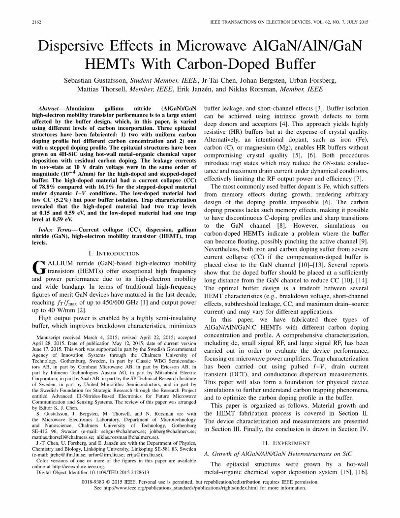
TLM measurements were performed on three positions oneach wafer (Table II). All materials show a similar contactresistance (Rc), demonstrating the feasibility of a repeatablerecessed ohmic contact process. The Rsh after devicefabrication is in good agreement with the preprocess andHall measurements (Table I).
The I–V characteristics were measured with a parameteranalyzer and are shown in Fig. 2(a) and (b). A significantlylower leakage current is seen for devices with a high andstepped carbon doping. The higher gate leakage for thelow-doped device can be affiliated with the pinchoffvoltage, which is more negative compared with thehigh-doped device. This will increase the slope of theenergy band in the AlGaN/GaN interface. Therefore, electrontunneling is more prominent, effectively increasing the gateleakage. Drain-induced barrier lowering (DIBL) is comparablysmall for the Stepped-C and High-C devices, but severe forthe Low-C device [Fig. 2(b) (inset)]. For Low-C HEMTs,the threshold voltage is continuously lowered as the drainvoltage increases and drops dramatically beyond 30 V. Thiscan be explained by high-energy electron injection into thebuffer. Table III contains extracted values of the subthresholdslope (SS), ON-resistance (RON), saturated drain current (IDSS),transconductance (gm), and DIBL. As expected the SS ishigher for devices with better electron confinement(High-C and Stepped-C). The variation in ON-resistancebetween the devices is due to differences in Rsh, Rc,and the device layout. The lower saturation current andtransconductance for the High-C device can be attributed tothe lower carrier density and carrier mobility in the material.The Low-C and Stepped-C devices are comparable in termsof saturation current, while Stepped-C has slightly highertransconductance.
Breakdown was measured using a drain current injectiontechnique [21] [Fig. 2(c)]. A sharp step is seen at the pinchoffvoltage for the High-C and Stepped-C materials. The stepis followed by a slope, where channel breakdown occurs.
Fig. 2. DC characteristics. (a) Drain current and transconductance atVDS = 10 V versus gate voltage. (b) Gate and drain currents at VDS = 10 Vas a function of gate voltage. Inset: threshold voltage versus drain voltage.(c) Drain–gate voltage normalized with LGD as a function of the gate–sourcevoltage while keeping a constant drain current.
TABLE III
DC CHARACTERIZATION RESULTS. ALL PARAMETERS EXCEPT
DIBL AND RON EXTRACTED AT VDS = 10 V
Eventually, gate breakdown occurs in the last region whereVDG saturates. The measurement of the Low-C material showsa different behavior with no sharp transitions. This is explainedby the electron injection in the low-doped buffer, and themajority of the drain current in this device is leaking throughthe buffer.
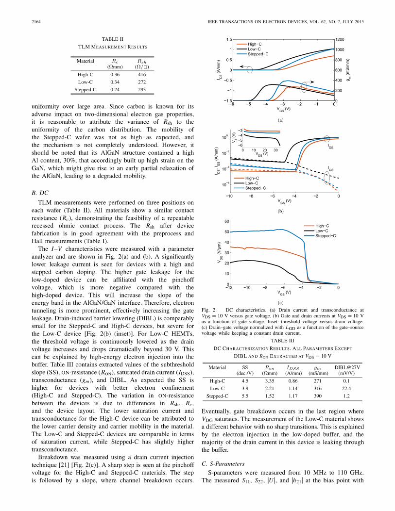
C. S-ParametersS-parameters were measured from 10 MHz to 110 GHz.
The measured S11, S22, |U |, and |h21| at the bias point with
GUSTAFSSON et al.: DISPERSIVE EFFECTS IN MICROWAVE AlGaN/AlN/GaN HEMTs WITH CARBON-DOPED BUFFER 2165
Fig. 3. S-parameter measurement. (a) Input impedance, S11. (b) Outputimpedance, S22. (c) Magnitude of U and magnitude of h21.
TABLE IV
SMALL SIGNAL CHARACTERIZATION RESULTS. PARAMETERS gm,ext ,
gds,ext , AND Cout EXTRACTED AT BIAS POINT FOR MAX fT
maximum fT are shown in Fig. 3. The devices have similarsmall signal behavior in terms of input and output impedance,while the device with Stepped-C has noticeably higher gainthan devices with High-C and Low-C. Table IV summarizesthe small signal characterization in terms of maximum fT ,maximum fmax, extrinsic gm , extrinsic gds, and extrinsic Cout.The small signal parameters were extracted at 285 MHz at thebias point for maximum fT (VGS = −2 V and VDS = 4 V forHigh-C, VGS = −3.5 V and VDS = 7 V for Low-C, andVGS = −2.5 V and VDS = 4 V for Stepped-C). TheStepped-C device shows the best performance in terms offT and fmax mostly due to its different layout and structure.The output capacitance and output conductance are similarfor all devices, and the extracted transconductance showsreasonable agreement with the values obtained from thedc characterization.
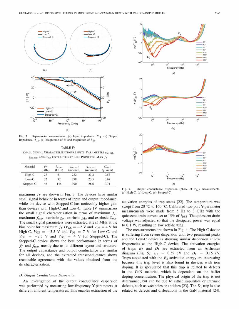
D. Output Conductance Dispersion
An investigation of the output conductance dispersionwas performed by measuring low-frequency Y-parameters atdifferent ambient temperatures. This enables extraction of the
activation energies of trap states [22]. The temperature wasswept from 20 °C to 160 °C. Calibrated two-port Y-parametermeasurements were made from 5 Hz to 3 GHz with thequiescent drain current set to 15% of IDSS. The quiescent drainvoltage was adjusted so that the dissipated power was equalto 0.1 W, resulting in low self-heating.
The measurements are shown in Fig. 4. The High-C deviceis suffering from severe dispersion with two prominent peaksand the Low-C device is showing similar dispersion at lowfrequencies as the High-C device. The activation energiesof traps E2 and D1 are extracted from an Arrheniusdiagram (Fig. 5); E2 = 0.59 eV and D1 = 0.15 eV.Traps associated with the E2 activation energy are interestingbecause this trap level is also found in devices with irondoping. It is speculated that this trap is related to defectsin the GaN material, which is dependant on the bufferdoping concentration. The physical origin of the trap is notdetermined, but can be due to either impurities or intrinsicdefects, such as vacancies or antisites [23]. The D1 trap is alsorelated to defects and dislocations in the GaN material [24].
2166 IEEE TRANSACTIONS ON ELECTRON DEVICES, VOL. 62, NO. 7, JULY 2015
Fig. 5. Arrhenius plot for identified traps in the dispersion measurements.
Fig. 6. DCT measurement showing the drain current derivative with respectto logarithmic time. Inset: DCT normalized with the quiescent current versuslogarithmic time.
In [25], a trap with similar activation energy (0.18 eV) isfound, and is suggested to be located at the surface. TheStepped-C device does not show any consistent shift in thedispersion peaks versus frequency and no activation energycould, therefore, be extracted.
E. Drain Current Transient
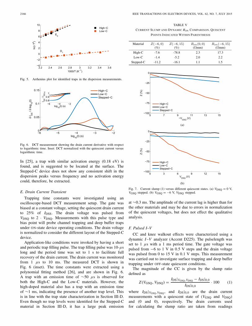
Trapping time constants were investigated using anoscilloscope-based DCT measurement setup. The gate wasbiased at a constant voltage, setting the quiescent drain currentto 25% of IDSS. The drain voltage was pulsed fromVDSQ to 2 · VDSQ. Measurements with this pulse type andbias point will probe channel trapping and deep buffer trapsunder ON-state device operating conditions. The drain voltageis normalized to consider the different layout of the Stepped-Cdevice.
Application-like conditions were invoked by having a shortand periodic trap filling pulse. The trap filling pulse was 10-µslong and the period time was set to 1 s to facilitate fullrecovery of the drain current. The drain current was monitoredfrom 1 µs to 10 ms. The measured DCT is shown inFig. 6 (inset). The time constants were extracted using apolynomial fitting method [26], and are shown in Fig. 6.A trap with an emission time of ∼50 µs is observed forboth the High-C and the Low-C materials. However, thehigh-doped material also has a trap with an emission timeof ∼1 ms, indicating the presence of another trap level. Thisis in line with the trap state characterization in Section III-D.Even though no trap levels were identified for the Stepped-Cmaterial in Section III-D, it has a large peak emission
TABLE V
CURRENT SLUMP AND DYNAMIC RON COMPARISON. QUISCENT
POINTS INDICATED WITHIN PARENTHESIS
Fig. 7. Current slump (1) versus different quiescent states. (a) VDSQ = 0 V,VGSQ stepped. (b) VGSQ = −6 V, VDSQ stepped.
at ∼0.3 ms. The amplitude of the current lag is higher than forthe other materials and may be due to errors in normalizationof the quiescent voltages, but does not effect the qualitativeanalysis.
F. Pulsed I–V
CC and knee walkout effects were characterized using adynamic I–V analyzer (Accent D225). The pulselength wasset to 1 µs with a 1 ms period time. The gate voltage waspulsed from −6 to 1 V in 0.5 V steps and the drain voltagewas pulsed from 0 to 15 V in 0.1 V steps. This measurementwas carried out to investigate surface trapping and deep buffertrapping under OFF-state quiescent conditions.
The magnitude of the CC is given by the slump ratiodefined as
Z(VGSQ, VDSQ) = IDS|VGSQ,VDSQ − IDS|0,0
IDS|0,0· 100 (1)
where IDS|VGSQ,VDSQ, and IDS|0,0 are the drain currentmeasurements with a quiescent state of (VGSQ and VDSQ)and (0 and 0), respectively. The drain currents usedfor calculating the slump ratio are taken from readings
GUSTAFSSON et al.: DISPERSIVE EFFECTS IN MICROWAVE AlGaN/AlN/GaN HEMTs WITH CARBON-DOPED BUFFER 2167
Fig. 8. Pulsed I–V measurements showing the dynamic IDS–VDS behaviorfor different quiescent states. (a) High-C. (b) Low-C. (c) Stepped-C.
at VGS = 1 V and VDS = 10 V. The current slump and dynamicRON is given for two quiescent states in Table V. The slumpratio versus VDSQ and VGSQ is shown in Fig. 7. The dynamicIDS–VDS characteristics for five different quiescent states areshown in Fig. 8.
The High-C device exhibits a major CC and drops to ∼75%of the reference current, while the Low-C device has veryslight CC throughout the VDSQ stepping. The Stepped-CHEMT shows similar VDSQ dependence as the Low-C device.However, the Stepped-C device has larger CC due to thedrop in drain current when a nonzero quiescent gate voltageis applied. The current slump performance of the Stepped-Cdevice is not entirely in line with the DCT measurements,which might be due to the normalization in the DCTmeasurements. The high-doped device shows large dynamicsin RON and severe knee walkout, with a near eightfold increasein ON-resistance. The significant increase in ON-resistance forthe high-doped device confirms that the D1-trap is located onthe surface.
Fig. 9. Delivered output power and drain efficiency versus delivered inputpower.
G. Load-Pull
Large signal device characterization was carried out usingan active load-pull setup [27] at a fundamental frequencyof 3 GHz. The devices were biased in Class AB, with aquiescent current of 15% of IDSS and VDSQ = 15 V.
An input power sweep was carried out for each device withthe load impedance optimized for maximum output power, andthe corresponding output power and drain efficiency is shownin Fig. 9. The Low-C and Stepped-C devices show comparableperformance and deliver similar output powers. The gain isslightly higher for the Stepped-C device, resulting in higherdrain efficiency at lower input powers and earlier saturation.As expected from the previous measurements, the large signalRF performance of the High-C device is degraded due to thesevere CC, effectively lowering the output power and drainefficiency. The maximum obtained output power is in goodagreement with estimations from pulsed I–V measurementsand amount to ∼0.9, 2.4, and 2.3 W/mm for High-C, Low-C,and Stepped-C, respectively.
IV. CONCLUSION
We have shown an extensive characterization ofGaN HEMTs fabricated from three different materialswith a high, low, and stepped carbon doping profile. Resultsshow that low leakage current and low CC can be achievedby optimizing the doping profile, thus maintaining good largesignal RF performance. In consistency with other reports,placing a highly doped buffer close to the GaN channelseverely degrades large signal RF performance due to thehigh CC. The Low-C and Stepped-C devices show similarperformance in terms of dc and RF, where the former offersslightly less CC and the latter lower leakage current.
The use of carbon doped buffer in [9] is shown to form afloating p-n junction, causing severe dispersion. The character-izations carried out in this paper indicates that the dispersionof C-doped GaN HEMTs is not as severe, and in line andeven better than the previous work on Fe-doped buffers. Thedispersion in C-doped buffers might, therefore, be due toother defects in the crystal not considered, but discussed,in [9]. A recent meta study on iron-doped buffers has founda trap with an activation energy of 0.6 eV, which is notdirectly related to the Fe-atoms in the buffer [13]. In thispaper, we have found a trap with a similar activation energy(E2 = 0.59 eV). We also observe another defect-related sur-face trap in the high-doped HEMT with an activation energy of
2168 IEEE TRANSACTIONS ON ELECTRON DEVICES, VOL. 62, NO. 7, JULY 2015
D1 = 0.15 eV. These traps may explain the different resultsin this paper and in [9]. Furthermore, as explained in [28],if vertical leakage paths exist between channel and buffer thedevice can still have low CC.
Trapping effects can be extremely dynamic and sensitiveto the stimuli. Depending on application needs, certain mea-surements can be focused on and different device propertiescan be emphasized by optimizing the buffer. Carbon is indeeda viable dopant for low-dispersive, HR buffers, and there isroom for further development and improvement of the dopingprofile.
REFERENCES
[1] K. Shinohara et al., “Scaling of GaN HEMTs and Schottky diodes forsubmillimeter-wave MMIC applications,” IEEE Trans. Electron Devices,vol. 60, no. 10, pp. 2982–2996, Oct. 2013.
[2] Y.-F. Wu, M. Moore, A. Saxler, T. Wisleder, and P. Parikh, “40-W/mmdouble field-plated GaN HEMTs,” in Proc. 64th Device Res. Conf.,Jun. 2006, pp. 151–152.
[3] M. J. Uren et al., “Control of short-channel effects in GaN/AlGaNHFETs,” in Proc. 1st Eur. Microw. Integr. Circuits Conf., Sep. 2006,pp. 65–68.
[4] P. B. Klein, J. A. Freitas, Jr., S. C. Binari, and A. E. Wickenden,“Observation of deep traps responsible for current collapse in GaNmetal–semiconductor field-effect transistors,” Appl. Phys. Lett., vol. 75,no. 25, p. 4016, Dec. 1999.
[5] Y. Wang, N. Yu, D. Deng, M. Li, F. Sun, and K. M. Lau, “ImprovedAlGaN/GaN HEMTs grown on Si substrates by MOCVD,” in Proc.10th Russian–Chin. Symp. Laser Phys. Laser Technol. (RCSLPLT) Acad.Symp. Optoelectron. Technol. (ASOT), Jul./Aug. 2010, pp. 68–71.
[6] S. Heikman, S. Keller, S. P. DenBaars, and U. K. Mishra, “Growthof Fe doped semi-insulating GaN by metalorganic chemical vapordeposition,” Appl. Phys. Lett., vol. 81, no. 3, p. 439, 2002.
[7] S. C. Binari, P. B. Klein, and T. E. Kazior, “Trapping effects in GaNand SiC microwave FETs,” Proc. IEEE, vol. 90, no. 6, pp. 1048–1058,Jun. 2002.
[8] J. B. Webb, H. Tang, S. Rolfe, and J. A. Bardwell, “Semi-insulatingC-doped GaN and high-mobility AlGaN/GaN heterostructures grownby ammonia molecular beam epitaxy,” Appl. Phys. Lett., vol. 75, no. 7,p. 953, Aug. 1999.
[9] M. J. Uren, J. Moreke, and M. Kuball, “Buffer design to minimizecurrent collapse in GaN/AlGaN HFETs,” IEEE Trans. Electron Devices,vol. 59, no. 12, pp. 3327–3333, Dec. 2012.
[10] E. Bahat-Treidel, F. Brunner, O. Hilt, E. Cho, J. Wurfl, and G. Trankle,“AlGaN/GaN/GaN:C back-barrier HFETs with breakdown voltage ofover 1 kV and low RON × A,” IEEE Trans. Electron Devices, vol. 57,no. 11, pp. 3050–3058, Nov. 2010.
[11] C. Poblenz, P. Waltereit, S. Rajan, S. Heikman, U. K. Mishra, andJ. S. Speck, “Effect of carbon doping on buffer leakage in AlGaN/GaNhigh electron mobility transistors,” J. Vac. Sci. Technol. B, Microelectron.Nanometer Struct., vol. 22, no. 3, pp. 1145–1149, 2004.
[12] V. Desmaris et al., “Comparison of the DC and microwave performanceof AlGaN/GaN HEMTs grown on SiC by MOCVD with Fe-doped orunintentionally doped GaN buffer layers,” IEEE Trans. Electron Devices,vol. 53, no. 9, pp. 2413–2417, Sep. 2006.
[13] M. Meneghini et al., “Role of buffer doping and pre-existing trap statesin the current collapse and degradation of AlGaN/GaN HEMTs,” inProc. IEEE Int. Rel. Phys. Symp., Jun. 2014, pp. 6C.6.1–6C.6.7.
[14] S. Rajan, A. Chakraborty, U. K. Mishra, C. Poblenz, P. Waltereit, andJ. S. Speck, “MBE-grown AlGaN/GaN HEMTs on SiC,” in Proc. IEEELester Eastman Conf. High Perform. Devices, Aug. 2004, pp. 108–113.
[15] U. Forsberg, A. Lundskog, A. Kakanakova-Georgieva, R. Ciechonski,and E. Janzén, “Improved hot-wall MOCVD growth of highly uniformAlGaN/GaN/HEMT structures,” J. Crystal Growth, vol. 311, no. 10,pp. 3007–3010, May 2009.
[16] A. Kakanakova-Georgieva, R. R. Ciechonski, U. Forsberg, A. Lundskog,and E. Janzén, “Hot-wall MOCVD for highly efficient and uniformgrowth of AlN,” Crystal Growth Design, vol. 9, no. 2, pp. 880–884,Feb. 2009.
[17] J.-T. Chen, U. Forsberg, and E. Janzén, “Impact of residual carbonon two-dimensional electron gas properties in AlxGa1−xN/GaN het-erostructure,” Appl. Phys. Lett., vol. 102, no. 19, p. 193506, May 2013.
[18] D. Nguyen, K. Hogan, A. Blew, and M. Cordes, “Improved processcontrol, lowered costs and reduced risks through the use of non-destructive mobility and sheet carrier density measurements on GaAsand GaN wafers,” J. Crystal Growth, vol. 272, nos. 1–4, pp. 59–64,Dec. 2004.
[19] M. Fagerlind and N. Rorsman, “Optimization of recessed ohmic contactsfor AlGaN/AlN/GaN heterostructures using C(V) characterizationof MSHM structures,” Phys. Status Solidi C, vol. 8, nos. 7–8,pp. 2204–2206, Jul. 2011.
[20] A. Malmros, H. Blanck, and N. Rorsman, “Electrical properties,microstructure, and thermal stability of Ta-based ohmic contactsannealed at low temperature for GaN HEMTs,” Semicond. Sci. Technol.,vol. 26, no. 7, p. 075006, Jul. 2011.
[21] S. R. Bahl and J. A. del Alamo, “A new drain-current injection techniquefor the measurement of off-state breakdown voltage in FETs,” IEEETrans. Electron Devices, vol. 40, no. 8, pp. 1558–1560, Aug. 1993.
[22] G. A. Umana-Membreno et al., “Low-temperature shallow-trap relatedoutput-admittance frequency dispersion in AlGaN/GaN MODFETs,”in Proc. Conf. Optoelectron. Microelectron. Mater. Devices, 1999,pp. 252–255.
[23] M. Meneghini et al., “Buffer traps in Fe-doped AlGaN/GaN HEMTs:Investigation of the physical properties based on pulsed and transientmeasurements,” IEEE Trans. Electron Devices, vol. 61, no. 12,pp. 4070–4077, Dec. 2014.
[24] J. H. Na et al., “A study of defects in AlGaN/GaN heterostructures,” inProc. Int. Conf. Molecular Bean Epitaxy, Sep. 2002, pp. 189–190.
[25] M. Faqir et al., “Characterization and analysis of trap-related effectsin AlGaN–GaN HEMTs,” Microelectron. Rel., vol. 47, nos. 9–11,pp. 1639–1642, Sep. 2007.
[26] M. Tapajna, R. J. T. Simms, Y. Pei, U. K. Mishra, and M. Kuball,“Integrated optical and electrical analysis: Identifying location andproperties of traps in AlGaN/GaN HEMTs during electrical stress,” IEEEElectron Device Lett., vol. 31, no. 7, pp. 662–664, Jul. 2010.
[27] M. Thorsell and K. Andersson, “Fast multiharmonic active load–pullsystem with waveform measurement capabilities,” IEEE Trans. Microw.Theory Techn., vol. 60, no. 1, pp. 149–157, Jan. 2012.
[28] M. J. Uren et al., “Intentionally carbon-doped AlGaN/GaN HEMTs:Necessity for vertical leakage paths,” IEEE Electron Device Lett.,vol. 35, no. 3, pp. 327–329, Mar. 2014.
Sebastian Gustafsson (S’13) received theM.Sc. degree in electrical engineering from theChalmers University of Technology, Gothenburg,Sweden, in 2013, where he is currently pursuingthe Ph.D. degree with the Microwave ElectronicsLaboratory Group.
His current research interests include RFmetrology and GaN HEMT characterization.
Jr-Tai Chen received the M.Sc. degree in electro-optical engineering from Tatung University, Taipei,Taiwan, in 2007.
He joined the Division of Semiconductor Materi-als, Department of Physics, Chemistry and Biology,Linköping University, Linköping, Sweden, in 2009.Since 2009, he has been involved in the MOCVDgrowth of GaN-based HEMTs structure on SiC andGaN substrates.
Johan Bergsten received the M.Sc. degree in engineering physics from theChalmers University of Technology, Gothenburg, Sweden, in 2013, wherehe is currently pursuing the Ph.D. degree with the Microwave ElectronicsLaboratory.
His current research interests include GaN HEMT fabrication andcharacterization techniques.
GUSTAFSSON et al.: DISPERSIVE EFFECTS IN MICROWAVE AlGaN/AlN/GaN HEMTs WITH CARBON-DOPED BUFFER 2169
Urban Forsberg received the M.Sc. degree inapplied physics and electrical engineering and thePh.D. degree in material physics from LinköpingUniversity, Linköping, Sweden, in 1998 and 2001,respectively.
He was with Norstel, Linköping, where hewas involved in epitaxial growth of SiC from2002 to 2004. He joined Linköping University,in 2004, where he has been involved in the devel-opment of the hot-wall technique for III–nitrides.
Mattias Thorsell (S’08–M’11) received theM.Sc. and Ph.D. degrees in electrical engineeringfrom the Chalmers University of Technology,Gothenburg, Sweden, in 2007 and 2011,respectively.
He is currently an Assistant Professor with theChalmers University of Technology. His currentresearch interests include the characterization andmodeling of nonlinear microwave semiconductordevices.
Erik Janzén received the Ph.D. degree insolid-state physics from Lund University, Lund,Sweden, in 1981.
He joined Linköping University, Linköping,Sweden, in 1989, where he has been a Professorwith the Department of Physics, Chemistry, andBiology since 1995, and the Head of SemiconductorMaterials since 2009. He has also been the Head ofSiC research at LiU since 1991.
Niklas Rorsman (M’10) received the M.Sc. degree in engineering physicsand the Ph.D. degree in electrical engineering from the Chalmers Universityof Technology, Gothenburg, Sweden, in 1988 and 1995, respectively.
He joined the Chalmers University of Technology, in 1998, where heis currently leading the microwave wide bandgap technology activities andinvestigating the application of graphene in microwave electronics.


![Trapping phenomena in AlGaN and InAlN barrier HEMTs with ...for the characterization of trapping phenomena in GaN-based HEMTs, as described in [17]. For example, gate (drain) lag measurements,](https://static.documents.pub/doc/80x56/60b82603333c894c11017fd1/trapping-phenomena-in-algan-and-inaln-barrier-hemts-with-for-the-characterization.jpg)


![Enhanced performances of AlGaN/GaN HEMTs with dielectric ...€¦ · 1DQR (QHUJ\ ˇ˙ ˇ j applications [3,4]. These problems are mainly caused by the relatively low-height Schottky](https://static.documents.pub/doc/80x56/5fdd9c79e5f2be72562a487d/enhanced-performances-of-algangan-hemts-with-dielectric-1dqr-qhuj-.jpg)

