Chapter 3 Innovative Structures for Routing and Configuration Abstract The goal of this chapter is to illustrate how emerging technologies can help to improve performance metrics of conventional Field-Programmable Gate Arrays structures. It is widely recognized that in traditional FPGAs, both the memory and the routing circuitry (with 43% of area for each contribution) represent the principal bottleneck to scaling and performance increase. In this context, we investigated 3D integration techniques for passive and active devices. The technologies surveyed will be a resistive memory technology, monolithic 3D integration and a vertical 1D transistor technology. In the previous chapter, we have seen that most area and performance metrics of modern Field Programmable Gate Array are limited by configurable interconnect and configuration memories. In this chapter, we will see how emerging technol- ogies might be used to improve these two aspects. 3D integration techniques will be surveyed. We will first discuss the exact context, in order to define the objectives of the designed blocks in a clear way. The various technologies sur- veyed are a resistive memory technology, monolithic 3D integration and a vertical 1D transistor technology. Each technology will be addressed with the following organization. After a brief literature review, we will describe the technology assumptions. Then, novel logic blocks will be presented and characterized. 3.1 Context and Objectives 3.1.1 Context Position In Sect. 2.1.3, the distribution of the area occupation between logic, memory and routing resources within an FPGA has been described. It shows that almost 45% of the silicon area is used only for the configuration memories, while the routing P.-E. Gaillardon et al., Disruptive Logic Architectures and Technologies, DOI: 10.1007/978-1-4614-3058-2_3, Ó Springer Science+Business Media New York 2012 47
Transcript
Chapter 3Innovative Structures for Routingand Configuration
Abstract The goal of this chapter is to illustrate how emerging technologies canhelp to improve performance metrics of conventional Field-Programmable GateArrays structures. It is widely recognized that in traditional FPGAs, both thememory and the routing circuitry (with 43% of area for each contribution)represent the principal bottleneck to scaling and performance increase. In thiscontext, we investigated 3D integration techniques for passive and active devices.The technologies surveyed will be a resistive memory technology, monolithic 3Dintegration and a vertical 1D transistor technology.
In the previous chapter, we have seen that most area and performance metrics ofmodern Field Programmable Gate Array are limited by configurable interconnectand configuration memories. In this chapter, we will see how emerging technol-ogies might be used to improve these two aspects. 3D integration techniques willbe surveyed. We will first discuss the exact context, in order to define theobjectives of the designed blocks in a clear way. The various technologies sur-veyed are a resistive memory technology, monolithic 3D integration and a vertical1D transistor technology. Each technology will be addressed with the followingorganization. After a brief literature review, we will describe the technologyassumptions. Then, novel logic blocks will be presented and characterized.
3.1 Context and Objectives
3.1.1 Context Position
In Sect. 2.1.3, the distribution of the area occupation between logic, memory androuting resources within an FPGA has been described. It shows that almost 45% ofthe silicon area is used only for the configuration memories, while the routing
P.-E. Gaillardon et al., Disruptive Logic Architectures and Technologies,DOI: 10.1007/978-1-4614-3058-2_3,� Springer Science+Business Media New York 2012
resources occupy 78% of the total area. In this chapter, we will address these twospecific parts of the FPGA: memory and the routing resources.
The requirement for storage in an FPGA could be considered at several levels.This distribution means that designers face various constraints. Table 3.1 shows astudy on memory requirements in an FPGA and gives an overview of associatedconstraints. We consider three different types of storage: high speed-data storage(fast flip-flops in the BLEs); configuration memories for logic (LUTs) and routing(Connection boxes and Switchboxes); and standalone Random Access Memories(Dedicated RAM Blocks). We focus on configuration memories (LUTs, CBs andSBs). These memories represent the biggest part of the FPGA area and share thesame properties. They are distributed throughout the logic circuit and are pro-grammed only a small amount of time. Traditionally, they are realized by SRAMcircuits. SRAMs ensure a technical homogeneity between the logic and the con-figuration part.
Nevertheless, SRAM memories are power- and area-consuming, as well asvolatile circuits. This means that the configuration must be loaded at each power-up, wasting time and power. Several circuits proposed the use of flash memories tocreate a non-volatile configuration [2]. However, the flash technology has a longprogramming time, and requires process co-integration. Indeed, floating-gatetransistor processes require more steps than high-performance CMOS processes.This obviously incurs extra fabrication costs and technical difficulties. Such a non-volatile technology is thus adapted only to niche applications. Hence, the tech-nology of configuration memories should be improved by using low-cost andnon-volatile technologies.
Furthermore, the largest part of the configuration memories are used to con-figure the routing circuits (82% of the memory area). The reconfigurable inter-connect alone occupies 45% of the area and introduces many active devices withinthe data paths. These devices impact directly the performance metrics of thestructure, by increasing the critical path delay of the reconfigurable architecture.Thus, it is of great interest to consider the problem of ‘‘routing’’ in a global way byaddressing the question of memory and the question of active configured devices atthe same time. Hence, while memory and routing could be addressed separately, itis reasonable to work on both sides try to compact this entire periphery.
Table 3.1 Specification estimation wrt. memory distribution through an FPGA (extracted fromXilinx Virtex6 architecture [1])
Distribution Even distribution throughout the architecture (fine-grainblocks)
Standalone blocks
48 3 Innovative Structures for Routing and Configuration
3.1.2 Objectives
In this chapter, we will propose the use of 3D techniques, to place devices in theback-end layers. Three different technologies will be surveyed. The differenceresides in the type of device that is placed in the back-end.
Firstly, Phase-Change Memories (PCM) will be used to embed a passiveresistive memory above the IC. Such a device is non-volatile and technologicallycompatible (i.e. indicating homogeneous integration) with the CMOS technolog-ical process. Hence, we will propose an elementary memory node, able to store aconfiguration in the resistive state of the memory and to provide it intrinsically to alogic gate. The storage of a configuration for a resistive memory is quite obvious.Nevertheless, such a technology is of high interest due to the low on-resistancecharacteristic of the memory. This makes it possible to directly use a memory as ahigh-performance switch and to embed it directly within the logic data paths. Wewill thus propose a switchbox circuit that uses simple resistive elements to replaceSRAMs and routing pass gates. All these circuits will be compared to their ele-mentary CMOS FPGA counterparts.
Secondly, we will use monolithic 3D integration technology to stack activedevices with a high via density. Such a process allows the stacking of 2D activedevices. We propose to split the configuration memories and the data path transistors.This allows technological improvement of both classes of circuit. We suggest acomplete integration of simple FPGA blocks, such as configuration memory, LUTand pass-gates, down to the layout level. In this way, we can provide a performanceevaluation of elementary nodes with regards to standard CMOS FPGAs.
The previous technology proposes an integration of devices in a 3D manner.Nevertheless, only 2D devices are stacked. We therefore propose an integrationprocess, which aims to realize a transistor (channel) in the vertical direction.A vertical NanoWire Field Effect Transistor process allows a vertical orientationof the active part of the transistor. It is then envisaged that several routing cir-cuitries (such as programmable vias and signal buffers) can be embedded in theback-end layer. In order to evaluate the performance metrics of the technology andcompare it to that of CMOS, we present a methodology based on TCAD simu-lations. TCAD will be used to model the elementary device, and electrical sim-ulations of simple circuits will be performed.
Finally, we will draw a global comparison between the technologies and extractsome overall conclusions.
3.2 On the Use of Resistive Memory Technologies
While Static Random Access Memories, Dynamic Random Access Memories(DRAMs) and Flash memories are predominant in microelectronics systems,thanks to their CMOS process compatibility, a large number of new memory
3.1 Context and Objectives 49
devices have been highlighted by the International Technology Roadmap forSemiconductors [3]. These memories are generally based on new physicalphenomena to retain the information and lift roadblocks to high density integra-tion. In this sub-chapter, we will focus on non-volatile resistive memories.
3.2.1 Introduction
Next-generation Non-Volatile Memory (NVM) has attracted extensive attentiondue to conventional memories approaching their scaling limits. Several types ofNVMs, such as ferroelectric random access memory, magnetic random accessmemory, and Resistive Random Access Memory (ReRAM), are being investi-gated. Among various NVMs, ReRAMs are typically composed of a simplemetal-switching element-metal structure, which has the merits of low powerconsumption, high-speed operation, high-density integration and CMOS processcompatibility.
Resistive memories, which can see their resistance vary depending on theapplied voltage, were intensively studied from the 1960s to early 1980s for deviceapplications [4]. Several materials can be envisaged to execute this desiredfunctionality. The type of material determines the physical phenomena that areused in the resistive change. For example, chalcogenide materials, semiconductors,various kinds of oxides and nitrides, and even organic materials were found tohave resistive memory properties. Hence, the architecture will depend to a largeextent on the technology. We can classify the technologies into two main families:Oxide Memories (OxM) and Phase-Change Memories.
Oxide memory state change is accomplished by the creation or the destructionof a conductive bridge through an oxide layer. This property is due to differentphysical phenomena, which depend on the material. The conduction formingmechanism is still not fully understood, and is currently under investigation. Thestructure is composed of a changeable resistance material sandwiched between twoterminal electrodes. Resistance change can be achieved by controlling the currentor voltage pulse applied to the electrodes, and the resistance state remains stablewithout being refreshed. To date, a number of different switching characteristicshave been observed in a variety of material systems; including NiO2 [5, 6], TiO2
[7], HfO2 [8], WOx [9], CuOx [10], TaOx [11]. In fact, it has become wellunderstood that a number of combinations of an oxide with metal electrodes canexhibit some kind of resistance switching behavior.
Phase-Change Memories are, as the name indicates, based on a material havingtwo different stable physical phases leading to two different resistances. As withOxM, several materials might be used such as GeSbTe [12], GeTe [13], GeTeC[14]. The PCMs are considered today to be one of the most promising candidatesfor the next generation of non-volatile memory applications [15]. The interest inPCMs is due to various advantages, including: better scalability (down to a fewnanometers) [16], faster programming time (of the order of few nanoseconds) [17]
50 3 Innovative Structures for Routing and Configuration
and improved endurance (up to 109 programming cycles) [18]. Some prototypes(such as a 60-nm 512-Mb [19] and a 45-nm 1-Gb [18] PCM technology) have beenpresented recently to showcase the viability of high-density standalone memoriesbased on PCM technology from an industrial point of view. The PCM technologyachieves the maturity required for large applications. We will focus on thistechnology. Nevertheless, it is worth pointing out that this work can be generalizedto any other resistive memory technology.
3.2.2 Phase Change Memory Properties and TechnologicalAssumptions
3.2.2.1 Physical Phenomena
A PCM device is based on the electrothermal-induced reversible phase transitionof a chalcogenide alloy between an amorphous insulating state (RESET) and apolycrystalline conductive state (SET). The polycrystalline phase is inherentlystable, as it is the lowest possible energy state of the system. On the other hand,retention instability affects the amorphous phase through two physical phenomena:spontaneous crystallization and low-field conductivity drift [20]. Recently, manyefforts have been made in order to achieve a better understanding of the physicalmechanisms which govern the behaviour of amorphous chalcogenides integratedin PCM cells [21–24]. Chalcogenide alloys are semiconducting glasses made byelements of the VI group of the periodic table, such as sulphur, selenium andtellurium. The best-known and most widely used chalcogenide alloy is Ge2Sb2Te5
(GST). GST can guarantee stability of programmed amorphous bits for more than10 years at 85�C [25]. While this can be considered to be sufficient for consumerapplications, many efforts are today devoted to the development of new chalco-genide materials to improve the high-temperature reliability of PCM technologiesin order to address the embedded memory market as well. Recent findings showthat GeTe thin films demonstrate a higher crystallization temperature than GST[12], as well as superior data retention performances when integrated in memorycells [13]. Furthermore, it is known that the crystallization process is affected bythe presence of foreign atoms in the material. For example it has been demon-strated that the Nitrogen doping of GST dramatically increases the stability ofamorphous phase [26, 27].
Indeed, by means of a careful control of Joule heating through the cell, it ispossible to electrically switch the chalcogenide layer between its two stableconfigurations, i.e. the high-conductive polycrystalline state and a low-conductiveamorphous one, as shown in Fig. 3.1. A sufficiently high voltage pulses heat intothe Phase-Change (PC) layer above the melting temperature of the material (Tm).A rapid quench follows and part of the chalcogenide alloy (depicted as an oval inthe PC layer) is stuck in the amorphous phase. The resulting memory cell is in a
3.2 On the Use of Resistive Memory Technologies 51
high resistance state (Fig. 3.1a). A lower but longer pulse is used to crystallize theamorphous region of the PC layer in order to achieve a low resistance memory cell(Fig. 3.1b).
3.2.2.2 Technological Assumptions
PCM technology is CMOS-compatible. As in Flash-NOR arrays, each mem-ory cell includes a storage phase-change node and a selector transistor in series(i.e. 1-resistor-1-transistor configuration). The memory element may be fabricatedeither just after the Si contact forming step at the Front-End-Of-Line (FEOL) levelor after the first steps of interconnections at the Back-End-Of-Line (BEOL) level,(e.g. on top of the Metal 0 or Metal 1 interconnect level) [28]. A schematic cross-section of the storage element architecture is shown in Fig. 3.2. The PCM device,formed of a PC layer with Bottom (BEC) and Top (TEC) Electrode Contacts, is
TEC
PCBEC
TEC
PCBEC
Voltage, Temperature [a.u.]
Voltage, Temperature [a.u.]
time [a.u.]
time [a.u.]
Logic 0
Logic 1
Tm
Tc
(a)
(b)
Fig. 3.1 Schematic of PCMdevice in Logic 0 (namedRESET) and Logic 1 (namedSET) configurations and ofthe programming pulsessuitable to obtain the states
M0 Gnd
M1TEC
PC
BECPCM
Fig. 3.2 Cross sectionalschematic showing a PCMdevice integration
52 3 Innovative Structures for Routing and Configuration
integrated between M0 and M1 interconnection level in the back-end-of-line. TheMOSFET selector (bottom) is fabricated in the front-end-of-line. This figuredepicts a pillar structure. The pillar approach is the simplest way to create a PCMdevice. First, a metallic heater is built. The heater is made by etching a via into theinter-layer dielectric and by filling it with a metal. The role of the heater is to helpto channel the current in order to increase its density and thus maximize the heatcontrol in the memory node. To improve the heater fabrication, several sublitho-graphic techniques have been proposed [29, 30]. After the heater metal deposition,the via is filled by chalcogenide alloys with a room temperature deposition.The top electrode is obtained by a final metal deposition.
3.2.2.3 Opportunities
Resistive memories, and especially the envisaged Phase-Change technology,represent truly promising opportunities for several aspects of design. Indeed,PCMs demonstrates non-volatile behavior at low cost. Such a property isobviously of high interest for all types of reconfigurable circuits, where a per-manent configuration circuit is strongly desirable. Furthermore, the technology isfully compatible with Back-End of Line and able to integrate the memories intothe 3rd dimension. This makes the resistive memories highly relevant as config-uration points, since we could expect promising size reduction through the inte-gration, above active silicon, of all area-hungry memories. Furthermore, theresistance of the on-state is typically below 1 kX (for example that of GeTe isaround 50 X). This is far lower than any MOS switch. Thus, it makes sense to usethem as a high performance switch replacement element for FPGAs, by directlyintroducing them into the logic data path. In such a way, we expect not only toimprove the size of the routing elements, but also to drastically reduce the delay ofimplemented circuits.
3.2.3 Elementary Memory Node
In this section, we present an elementary circuit, based on a PCM non-volatileresistive memory, used to move most of the configuration part of reprogrammablecircuits to the back-end, reducing their impact on front-end occupancy. Such amemory node is dedicated to drive multiplexer (MUX) inputs or pass-gates. Thememory node is programmed by injecting a certain current through it; while theinformation has to be read as a voltage level. Furthermore, it shall allow a layout-efficient line sharing.
3.2 On the Use of Resistive Memory Technologies 53
3.2.3.1 Concept
The elementary memory node is presented in Fig. 3.3. The circuit consists of tworesistive memory nodes connected in a voltage divider configuration between twofixed voltage lines. A transistor is also connected between the ground and theoutput node of the cell. It is used to select the node during the programming phase.The output is designed to place a fixed voltage on a classical standard cell input.Read operations are intrinsic to the structure, while programming is an externaloperation to be performed on the cell.
The voltage divider is used in this topology to execute intrinsically theconversion from a data stored in a variable resistance to a voltage signal.Figure 3.4 shows a configuration example where the node stores a ‘1’. Theprogramming transistor is placed in the off-state by the non-active Prog_Enablesignal, so that the ground is disconnected from the output. The resistive memory(1) that is connected to the Vdd line, is configured into the crystalline state, so itsassociated resistivity is low (a few kX). The other memory (2), connected to Vss, isin the amorphous state with high resistivity (close to 1 MX). As a consequence, avoltage divider is configured and the output node is charged close to the voltage ofthe branch with a high conductivity. The logic levels depend on RON and ROFF asin the following relations:
010 ¼ Vdd � RON
RON þ ROFFðVdd � VssÞ 000 ¼ RON
RON þ ROFFðVdd � VssÞ
It is also worth noticing that in continuous read operation, a current will beestablished through the resistors. This leads to a passive current consumptionthrough the structure depending to the following relation:
I ¼ Vdd � Vss
RON þ ROFF� Vdd � Vss
ROFF
As an illustration, the PCM technology off-resistance is around the MX value.At Vdd = 1 V, the technology yields to a leakage current of 1lA. This is obviouslytoo high for a viable industrial solution. Nevertheless, this static current could bereduced by the choice of a memory technology maximizing the ROFF value(e.g. OxRAM technology exhibits off-resistance bigger than the GX).
54 3 Innovative Structures for Routing and Configuration
3.2.3.2 Programming Circuitry
Figure 3.5 presents the programming phase of the node. While the programmingtransistor is placed in the on-state by setting the Prog_enable signal, the fixed readvoltage sources are disconnected from the top lines and replaced by the programmingunit. Then, a programming current is applied sequentially into the resistive memoriesto change their states. Programming currents are drained to the ground.
As each cell has its own selection transistor, the programming lines can be sharedin a standalone-memory-like architecture, as shown in Fig. 3.6. The programmingunit is composed of three different elements. A programming pulse generator handlesthe creation of the programming pulse with the correct waveforms. The program-ming signals are then routed by two stages of multiplexers. They are routed throughBLXA or BLXB lines in order to program memory A or B respectively. We also notethe Program/Operation selectors. Their aim is to route static voltages when the nodesare not under programming. During the programming, the selection of a node isensured by the WLX signals. Thus, the choice of the memory node to program is madeat the programming unit level, through the selection realized by the Program/Operation selectors and the Memory Program selector.
3.2.4 Routing Elements
In the previous section, we presented a memory node, which aims to replace theconfiguration memories in configuration memory-intensive circuits. The node isintended to drive any logic gate and is thus a straightforward replacement part for
Vdd Vss
Hi Lo
1 2
Output~Vdd
Fig. 3.4 Node in readconfiguration
Iprog
Output~Gnd
Fig. 3.5 Node in writeconfiguration
3.2 On the Use of Resistive Memory Technologies 55
SRAMs. In Sect. 3.2.2.3, we observed that the use of Resistive RAMs is also ofgreat interest for performance improvement of data paths, thanks to their lowon-state resistance.
3.2.4.1 Concept
FPGA switchboxes represent the most demanding circuits in terms of routingperformance. We thus propose to replace the traditional pass gates with thestructure shown in Fig. 3.7. Figure 3.7a shows a schematic diagram of a 2 9 2crossbar structure using PCM resistances. At each cross point in the crossbar,routing elements are placed. They are able to create any combination of connec-tions between the North/South/East/West terminals of the cross point. Theserouting elements are built with a similar structure as those of CMOS, wherebytwo-terminal PCMs replace pass-transistors (Fig. 3.7b). An on-connection isrealized by programming the PCM, situated between the two wires that it shouldconnect, to a low resistance state. With this structure, we build an ‘‘intelligentcross point’’, which is able to merge the programming node and the pass switch ina single device. The device is embedded in the Back-End levels as a via, andreplaces a five-transistor SRAM and a four-transistor pass gate. Furthermore, sincethe PCM itself performs the switching in the data path, its own on- andoff-resistance values also have a direct impact on the circuit performance.
Once programmed, the cell behavior is purely static. Conductive paths arecreated by the resistive networks as illustrated in Fig. 3.7c. In this figure, weobserve three conductive paths through the box: InW OutN, InN OutE, andInE OutW. In this structure, the number of reachable inputs/outputs depends onthe Ron/Roff ratio. In such crossbar architecture, the lowest resistive memory pathsdefine the connections. Nevertheless, currents will also be established in the highconductive bridges. Thus, the discrimination between a conductive and anon-conductive path rely only on the path resistance difference. We consider thesituation of Fig. 3.7c. The path InE OutW goes through two on-resistances. This
Programming generator
Vss
Vdd
Iprog
WL0 WLN
BL0A
BL0B
Memory Program Selector
Program/OperationSelectors
Fig. 3.6 Line sharing illustration in standalone-memory-like architecture
56 3 Innovative Structures for Routing and Configuration
resistance is thus 2 Ron. The path InE OutS goes through a unique off-resistance.The resistance is thus Roff. In this example, it is not possible to discriminate thepath if Ron/Roff is too low (i.e. two in the extreme bound). More precisely, thelongest on-resistance path of the structure should be compared to the shortest off-resistive path. The tolerable Ron/Roff ratio is thus given by:
Longest Path Ron
Shortest Roff� 1000
(with 1000 an arbitrary choice to ensure a significant discrimination). More con-siderations on the structure can be found in [31].
3.2.4.2 Programming Circuitry
A PCM is programmed by applying a pulsed signal between its two terminals. Thisconducts the PCMs of the switchbox to be addressed sequentially. In the structure,the PCM is selected by connecting one terminal to the programming unit, while theother is grounded. When a unique memory is select, the other PCM terminals areleft floating to avoid parasitic programming. After the selection, the programmingunit drives the desired set or reset pulse to program the resistivity state.An example of sequential programming is shown in Fig. 3.8.
The programming voltages and timing pulses required to program the PCMsmay be applied through the drivers at the inputs and the outputs of the switchboxes(Fig. 3.7a). Figure 3.9 shows a possible structure for these drivers. They are usedfor the electrical interface between signal channels and the programming unit,which generates the configuration waveforms. Figure 3.9a shows a possible inputdriver, while Fig. 3.9b shows the implementation of the output driver. Asexplained, the buffers must allow the connection of the nodes to the programmingunit, to the circuit or to a high-impedance node. This last possibility is handled bythe three-state multiplexers and buffers. The programming unit is routed by themultiplexer for the input, and through a single pass transistor for the output.
In W
Out W
Out E
In E
In S Out S
Out N In N
North
South
West East
In W
Out W
Out E
In E
In S Out S
Out N In N(a) (b) (c)
Fig. 3.7 a PCM-based 2 9 2 switchbox architecture b zoom on the cross point structurec example of programmed switchbox (memories in off-state are not shown for clarity)
3.2 On the Use of Resistive Memory Technologies 57
3.2.5 Performance Characterization
3.2.5.1 Methodology
In order to characterize the performance of the node, we extracted the area, thewrite time and the programming energy as metrics. The extraction is based onnode complexity and interpolation from ITRS figures [32]. Then, comparison withmemory elements traditionally used in FPGA, such as MOS SRAM 5T [33] andflash memories storage LUT elements [34], are used to benchmark the structure.
Since the technology enables most of the configuration circuit to be placed inthe back-end levels, the area metric corresponds to the front-end projection of theimpact of the memory node. The write time and the programming energy are alsoconsidered. Even if the use of non-volatility makes these considerations far lesscritical, it is still of interest to improve them, in order to enable low power and fastreprogramming.
3.2.5.2 Performance Estimation
Table 3.2 shows some characterization results in terms of area and write time forthe proposed solution compared to traditional FPGA memory nodes. Considering
IPR OG IPR OG
IPR OG
1) 2) 6)
: Unprogrammed cells : Programmed cells
Fig. 3.8 Example of switchbox programming sequence
3-state
MUX
Programming unit
In
Iprog
Sel En
Out
Sel
Switchbox Switchbox 3-state
Programming unit
(a) (b)Fig. 3.9 Input (a) and output(b) drivers for PCM-basedcrossbar
58 3 Innovative Structures for Routing and Configuration
that all these elements are driving an equal load, we omitted the pass transistor atthe output node in our simulations. Thus, the SRAM cell is considered to be a5-transistor (5T) structure. The Flash topology is implemented by 2 Flashtransistors [35]. The Magnetic RAM implementation is realized by an unbalancedflip flop as proposed in [36]. In fact, this allows efficient separation of theprogramming path from the data path.
We see that the proposed PCM cell is the most compact solution, even with theimpact of the programming current on the access transistor. This advantage is dueto the reduction of the memory front-end footprint to only one transistor, comparedto five for the SRAM cell, and compared to two for the Flash solution (one pull-uptransistor coupled to a floating gate transistor). We should remark that PCMs offera significant reduction in writing time for non-volatile memory technologies, aswell as a consequent reduction in writing energy. In our context, it is possible toreduce the area by a factor of 1.5 and the writing time by a factor of 16.6 and theprogramming energy by a factor of 500 compared to an equivalent flash tech-nology. However, the programming energy is about ten times larger than in theflash technology. Compared to another emerging equivalent non-volatile magneticresistive technology, we can observe that the proposed structure improves the areaby a factor of 3.8. This is due to the chosen structure for the magnetic resistivenode, which is based on an area-hungry unbalanced flip-flop. Nevertheless, it isimportant to highlight that the PCM-based node is slightly slower for reconfigu-ration, with a 33% difference as compared to magnetic memory. Finally, while thewriting time is slower, the required programming energy is reduced by a factor of50 as compared to the magnetic technology, which requires energy to create theprogramming magnetic field. We should therefore consider that this result isstrongly dependent on the technology used. In this work, we considered Ther-mally-Assisted-Switching (TAS) MRAM technology. While this technology hasthe same level of maturity as PCM, it also requires a large programming energy(between 100 and 150 pJ per cell). Most advanced writing schemes, such as SpinTransfer Torque [38, 39] allow further reduction of writing energy to the range of3 pJ per cell.
Table 3.3 shows some characterization results in terms of area and writing timefor the solution and conventional FPGA memory nodes. The SRAM-based node is
3.2 On the Use of Resistive Memory Technologies 59
formed by four 4-input multiplexers, programmed by 5T SRAMs. The Flash-basedsolution is taken from [35], while the MRAM-based solution is taken from [36].In this work, two flash transistors are used to replace a combination of one SRAMand one pass gate. The structure of the switchbox is considered to be the envisagedPCM structure. We should note that a GeTe technology [14] with a very low on-resistance value is envisaged, as it corresponds to the requirements for a highperformance switch.
We see that the proposed PCM switchbox is the most compact solution, evenwith the impact of the programming current on the access transistor. Thisadvantage is due to the reduction of the memory front-end footprint to only metallines, compared to five transistors for the SRAM cell and two transistors for theFlash solution (one pull-up transistor coupled to a floating gate transistor). It is alsoworth noticing that PCMs offer a significant reduction in write time versus flashtechnology. In our context, it is possible to reduce the area by 3.4 and the writetime by 16.6 as compared to an equivalent Flash technology. Another importantmetric is the data path resistance. In the context of a logic signal propagatingthrough the switchbox, we observe that the on-resistance of PCM is very lowcompared to the other solutions. In fact, all the other solutions still use a MOStransistor to realize the data path switch. Hence, since the on-resistance isdecreased by a factor of 182, this means that a reduction of the propagation time isexpected. From the point of view of the off-resistance however, we observe theopposite, since the off-resistance follows the same trend as the on-resistance. Thismeans that the off-resistance decreases by a factor of 144, and since off-resistanceimpacts directly on switch leakage, this decrease is likely to worsen static powerdissipation and logic levels. However, this could be mitigated by the fact that theRon/Roff ratio has not decreased—on the contrary, PCM cells demonstrate animproved ratio with a value of around 1/20,000, with respect to the value of 1/15824 obtained for the other solutions. The ideal solution will require a low Ron
value, while the Ron/Roff ratio should be increased with respect to CMOS.
60 3 Innovative Structures for Routing and Configuration
3.2.5.3 Discussion
The presented performance metrics make the solutions built around resistivememories of high interesting for the purposes of reconfigurable applications.Indeed, we showed that it is possible to create a compact configuration memorynode that can store a logic level in two resistances. This logic node improves thesize as compared to flash memories by 1.59. While this 33% reduction in areareduction is significant, it is worth noticing that the limitation is due to theprogramming transistor. Indeed, the selection transistor size is dictated by the levelof current to be driven to the cell being programmed. While the requiredprogramming current is large, the programming energy remains the lowest overthe benched technologies. Other technologies might be envisaged in order tofurther reduce the programming current. First of all, other PCM technologies, suchas GeTe or GeTeC [14], require smaller currents for programming compared tostandard GST. It is then possible to migrate to other resistive memory technolo-gies. For example, OxRAM requires less current overall for their programming,and will lead to more compact configuration nodes [40].
Concerning the routing part, we propose to introduce the PCM directly into thelogic data path. This is of interest from two points of view. First, we obtain an areareduction of a factor of 3.4 as compared to flash. However, the most interestingadvantage comes from the technology: the ReRAM technology is shown to have amuch lower on-resistance than CMOS switches, which should lead to significantreductions in propagation delay in complex logic circuits. While the well-knownGeSbTe-based PCM technology has a ‘‘quite high’’ Ron value, it is attractive tolook at new PCM materials or new technologies. In particular, special alloys suchas GeTeC and GeTe [14] have demonstrated a very small on-value, well-suited tothe requirements of the routing structures. Nevertheless, it will be necessary also tostudy the reliability of the proposed switchboxes as well as the data retention timein the structure. Resistive memories are switched by a controlled current or voltageapplied to or through them. Nevertheless, the switching behavior is generally morecomplex, as far as timing and environment (e.g. temperature) must also beconsidered. Unpredictable signals are flowing in the data path. Unpredictablemeans that the signals depend on the application. Thus, the memories introducedin the flow maybe switched to unwanted states leading to an unreliable structure.
3.3 On the Use of Monolithic 3D Integration Process
In the previous section, we looked at a technology, which allows a passive resistivememory device to be embedded into the back-end levels. While this approach isadvantageous for memory or routing structures, the elements are only passive.It then appears interesting to assess the interest of 3D integration, in order todiversify the functionality of above IC devices. In this section, we propose the use
3.2 On the Use of Resistive Memory Technologies 61
of a monolithic 3D integration technology to stack two active layers. Thisrepresents a first step towards the use of active devices in a 3D scheme.
3.3.1 Introduction
For several decades, the semiconductor industry has invented new approaches toincrease integration density and transistor performance, the main vector for thisbeing MOSFET scaling.
In this context, the IC integration in three dimensions appears to be a promisingalternative path to scaling, and to some extent would avoid the huge investmentsrequired by scaling. While the concept is not entirely new [41], the development ofthe technology has witnessed significant growth over the last decade. In particular,the technology of Through-Silicon-Vias (TSVs) is currently the reference for 3Dtechnology processes. A TSV could be defined as a large via built across thesubstrate, in order to contact the active front-end to the reverse-side of the chip.Bumps are then used to contact the dies between them, as shown in Fig. 3.10.
While such integration is challenging due to TSV density requirements (leadingto a double specification of TSV aspect ratio and wafer thickness), the process ismature enough for industrial applications [42]. However, there are still somehurdles to face. Table 3.4 depicts the principal characteristics of TSV processes[43]. It is worth noticing that TSVs are quite area-hungry with diameter up to 5 lmand pitch up to 10 lm. This means that the connection density is quite poor (from400 to 10,000 TSVs/mm2) and this results in a loss of active size. Thus, designersare limited to high level interconnect, such as memory/core communication.However, this segregation is of great interest for performance, since processes willbe tuned to optimize each layer to a given class of application (low power, generalpurpose).
In a reconfigurable application, a large number of interconnections arerequired if separation between memory and logic is to be envisaged. Thismeans that other integration processes should be used, to overcome the limi-tations of connection density. In an FPGA, connections between memory andlogic are done at gate level. We estimate the required density at about 500,0003D contacts/mm2. Thus, instead of processing the layers separately and stackingthem a posteriori, it is possible to use monolithic sequential integration. In amonolithic integration, the circuit is processed from the bottom to the top. This
62 3 Innovative Structures for Routing and Configuration
means that the stacked layers are build by a set of technological steps above thealready processed stack.
Such an integration scheme is promising for several reasons. Firstly, it enables amuch higher via integration density. In fact, the contacts use a planar scheme step,as opposed to TSVs. Thus, it is possible to obtain alignment accuracy in the rangeof lithographical precision (around 10-nm), whereas TSV alignment accuracy is inthe range of 1 lm. However, monolithic integration gives rise to other issues.In particular, conversely to parallel integration, where the layers are processedseparately, it is necessary for the fabrication of the top transistors not to degradethe performance of the bottom layer transistors. This means that the top layerthermal budget is limited and that processes have to be thought through inconsequence.
3.3.2 Technological Assumptions
As briefly introduced above, the monolithic 3D integration process integrates atleast two layers of active silicon. These layers are processed sequentially, as shownin Fig. 3.11. The principal process steps are (a) the realization of the bottomtransistor (b) the deposit of the top film silicon and (c) the realization of the toptransistor. Several constraints appear at each step.
The first transistor layer must be optimized in order to improve its robustnessto temperature. It is worth nothing that the second active transistor layer willhave an impact on the first layer and thus the thermal robustness of the bottomlayer is critical. The maximal thermal budget for subsequent steps is limited bysalicidation. In fact, standard NiSi dewetting occurs in only 3 min at 600�C.To obtain a low resistance access with processes around 600�C, a salicide sta-bilization procedure has been demonstrated in [45]. This salicidation approach isbased on an optimized W-NiPtSi-F. With this technology, the salicide is stable at600�C, which is considered to be the maximal thermal budget for all the sub-sequent steps.
The second step corresponds to the realization of a high quality top film. Whileseed window techniques were first used in the literature [46], they lead tocrystalline defects, poor thickness control and density loss. It is thus better to used
Table 3.4 Density survey of TSV technologies [43]
Diameter(lm)
Pitch(lm)
Density(TSVs/mm2)
CMOS 65-nmgate equivalent
Low densityTSVs
20 50 400 1,250
High densityTSVs
5 10 10,000 50
3.3 On the Use of Monolithic 3D Integration Process 63
molecular bonding [45], where a blanket Silicon-On-Insulator wafer is transferredon top of the processed MOS wafer. This step plays a major role in alignmentaccuracy, since the alignment occurs after bonding, conversely to parallelintegration [47].
A low temperature Fully Depleted Silicon-On-Insulator is then processed on thetop film. Due to the limited thermal budget (600�C), it is not possible to performthermal activation of dopants (around 1,000–1,100�C). The process uses a solidphase epitaxial re-growth [48], which consists of pre-amorphization of the topfilm, followed by dopant implantation and finishing by a re-crystallization at600�C.
Finally, 3D contacts are realized using the same contact techniques as instandard processes. Only one lithography step is required for all contacts. Thecontact realization step is illustrated in [45], where W (tungsten) plugs existbetween the top and bottom layers. The process has been validated for severalsimple cases, such as SRAM memories or inverter cells [48, 49].
3.3.3 Elementary Blocks
In order to evaluate the opportunity of the monolithic 3D integration process,elementary nodes for configurable logic have been designed. The blocks that havebeen chosen are a 3D Look-Up Table and a 3D Cross point. The global idea is toplace the configuration memory just above the circuit that requires it.
3.3.3.1 LUT Impact
Our design assumption is that the top layer is used to implement configurationmemories in a standard CMOS approach. Hence, it is quite straightforward todevelop a two layer 3D look-up table. In Fig. 3.12, the layout and the schematic of a1-bit Look-Up Table are depicted. While the structure is too simple for any archi-tectural considerations, it is useful for the purposes of technological demonstration.
BOX
TILD
BOX
PolyTiNHfO2
BOX
TiNSalicided access
HfO2
Poly
(a) (b) (c)
Fig. 3.11 Cross-sectional view of 3D monolithic steps—a optimized bottom FDSOI processb high quality top film deposition c low temperature top FDSOI process [44]
64 3 Innovative Structures for Routing and Configuration
Two configuration nodes are thus placed above a multiplexer circuit. Thedimensions of the multiplexer are largely relaxed, due to limitations on the metallayers available for the technological demonstrator.
In this way, we could consider that only a small amount of size is used for thestructure, in addition to the multiplexer. Furthermore, while we observe a strict sep-aration between the configuration memory part and the data path multiplexer, it ispossible to optimize the technological process to reach specific properties. Especially,it is envisaged to have a low-leakage—low-power process for memories, while theactive data paths are created using high performance transistors. This makes theimplementation highly promising for circuits requiring large configuration memory.
3.3.3.2 Routing Structure Impact
Using the same technological assumptions, we also propose a routing cross point.The cross point is built around a two-transistor pass-gate, which is driven by astatic memory. The memories and data path will be split and placed on differentlevels. Memories are placed on top of the cells that directly use their information,and thus a large reduction in the number of wires is observed. Two differentstructures have been realized.
Figure 3.13 shows the cross point using register-based memory. It is worthnoticing that, in this circuit and conversely to the LUT, the memory dominates thedimensions of the cell. Indeed, the pass-gate, even when considering a large sizetransistor, has low requirements in terms of the metal layers, and thus its
BOT
MUX2:1 (bottom)
Configuration nodes (top) x2
TOP
D0
D1
REG
REG
OUT
S0SCLK SDI
SDO
TOPBOTTOM
Fig. 3.12 Two layer monolithic 3D based 1bit Look-Up Table—layout and schematic
3.3 On the Use of Monolithic 3D Integration Process 65
implementation below the memory is kept at the front-end. We also point out theH-shape of the pass-gate, which is a side effect of the optimization of contactsbetween the bottom, the top and the first metal layers.
The above implementation uses a configuration node, which could be pro-grammed serially. This is obviously of high interest for FPGAs, since it allowsmemory cascading and thus simplifies the programming circuitry. Nevertheless, inthe context of separation between logic and configuration memory in a 3D process,it is of interest to use a standalone memory approach. Hence, a typical SRAMorganization could be envisaged on the top layer with word lines and bit linescrossing through the circuit, while the FPGA data path is found below. Figure 3.14shows a possible implementation of an SRAM memory with a pass-gate in a verycompact 3D implementation.
3.3.4 Performance Characterization
3.3.4.1 Methodology
The performance metrics of the presented elementary blocks have been extractedfrom layout and electrical simulations.
OUT
TOPBOTTOM
IN
REGQ !Q
SCLKSDI SDO
BOT
Pass Gate (bottom)
Configuration nodes (top)
TOP
3-D Crosspoint
Fig. 3.13 Two layer configurable cross points (configuration node based)—layout and schematic
66 3 Innovative Structures for Routing and Configuration
The simulations are realized using the Synopsis HSPICE electrical simulator.This simulator allows a fast and accurate simulation for CEA-LETI’s homemademodel.
The metrics will be area, delay and power consumption. The area is extractedconsidering the layouts. The test chip uses two different set of design rules forfront-end and back-end. In order to demonstrate the capabilities of the technologywith a relatively low cost, the front-end can be scaled down to the 16-nm node,while the back-end uses a 65-nm lithographic node. Nevertheless, in order to becompared fairly with existing technology, all the dimensions used in the layoutsuse an equivalent 65-nm lithographic node. The delay is assessed by electricalsimulation and broken down into the intrinsic delay and the load delay (expressedas the Kload factor). The power consumption is extracted by electrical simulationwith an FO4 load. The circuit is operated at the gate’s maximum achievablefrequency with the FO4 load. This means that rise and fall time are chosen inaccordance to 5s charge and discharge. The related frequency obviously dependson the circuit. At this frequency, we swept all possible input vector combinationsand we averaged the power consumption.
OUT
TOPBOTTOM
BL
IN
BL
WLWLBOT
Pass Gate (bottom)
SRAM cell(top)
TOP
3-D Crosspoint
Fig. 3.14 Two layer configurable cross points (SRAM cell based)—layout and schematic
3.3 On the Use of Monolithic 3D Integration Process 67
In order to compare the performance of the 3D FDSOI, we compare all metricsto a standard industrial low power 65-nm process. In order to differentiate the gaindue to the FDSOI technology and that due to the 3D implementation, we alsoperform the evaluation of the equivalent circuit in 2D FDSOI. We should mentionthat the electrical model is the same for both bottom and top transistors and thatparasitic post-layout extraction is not available in the design kit as used. Thus,comparisons in terms of performance and power will not differ from 2D and 3Dimplementation of the FDSOI cells.
3.3.4.2 LUT Performance
Table 3.5 shows the performance comparisons for a very simple two-input LUTtest case. The considered circuit corresponds to that presented in Fig. 3.12.Concerning the area, we obtain a 2.039 improvement in regards to 2D bulk. Thisfigure is mainly due to the stacked integration of the memory on top of themultiplexer. It is also worth mentioning that the 2D FDSOI implementation islarger than the 2D bulk one. This result is counter-intuitive, since the lithographicnode used is the same in both cases. However, we should note that the 2D FDSOIlayout has been carried out following regular layout techniques, as well as somerelaxed technological demonstrator rules. This clearly leads to larger cell imple-mentations than in an equivalent non-regular bulk process.
In terms of performance and power, an improvement of 1.629 in intrinsic delaycan be observed, as can figures of 6.119 in load influence factor and 29 indynamic power at 1 GHz. The contributing reasons for these good numbersare twofold. As already stated, the technology is compliant to low-power high-performance circuits. Nevertheless, the improvements are also due to 3D inte-gration. It is possible to group the low-power optimized circuits on one layer,while performance-optimized blocks are grouped on another. This allows specificprocess optimization, but it also allows the dimensions of some transistors to berelaxed. For example, in this context of LUT, it is possible to size the multiplexerto be quite large, while the memories are placed on top. This strategy leads to ahigh-performance multiplexer, placed under the necessarily area-hungrymemories.
Table 3.5 Evaluation of Look-Up Table performance
LUT265-nm node
Area (lm2) Intrinsic delay (ps) KLoad
(ps.fF-1)Average powerat 1 GHz (lW)
2D LP bulk 64.48 85.08 36.29 46.902D FDSOI 122.57 52.52 5.94 23.233D FDSOI 31.7 52.52 5.94 23.232D bulk versus 3D FDSOI 9 2.03 9 1.62 9 6.11 9 2.022D FDSOI versus 3D FDSOI 9 3.87 – – –
68 3 Innovative Structures for Routing and Configuration
3.3.4.3 Cross Point Performance
Table 3.6 shows the performance evaluation of 3D cross points. As previouslydescribed, two different cross point schemes are studied. The difference betweenthe two cross points resides in the configuration. One is based on a shifterconfiguration node and the other is based on an SRAM.
In terms of area, we should note that the SRAM-based cell is the most compactone, with an improvement factor of 2.939 compared to 2D bulk. This is obtainedmainly due to the compactness of SRAM cells, where each transistor and layout isoptimized to obtain the best density. Nonetheless, due to its greater size, theconfiguration-node based cross point improves the area by ‘‘only’’ 1.489. It isworth noticing that this cross point implementation embeds all the circuitryrequired to program the node in a shift register manner. Thus, it appears obviousthat this implementation is larger compared to the fully optimized SRAM-basedimplementation.
In terms of performance, the intrinsic delay is shortened by 1.69 and 3.19 forthe configuration-node based implementation and the SRAM-based implementa-tion, respectively. The load factor is almost the same with a gain of 1.069. Thedifference comes mainly from the pass-gate cell. It is in fact possible to use largertransistors in the SRAM-based implementation; indeed, since the cell is morecompact, the shape of its layout facilitates its placement and efficient connection ofthe bottom pass-gate.
Finally, in terms of dynamic power, we observe a 3.19 improvement at 2 GHzfor the configuration-node based cell, and 2.19 for the SRAM-cell, compared tobulk. These numbers come mainly from the use of FDSOI, which is an intrinsiclow power technology. The difference between the two memory structures is dueto pass-gate sizing. Since most of the contribution to power originates in the datapath, these results can again be attributed to the sizing of the pass-gate. In theSRAM-based case, the transistor is larger and leads to larger power consumptionduring the signal drive.
Table 3.6 Evaluation of cross point performance
65-nm node Area (lm2) Intrinsic delay (ps) KLoad
(ps.fF-1)Average powerat 2 GHz (lW)
2D LP bulk 15.83 0.44 0.71 0.123D FDSOI
Configuration node10.66 0.28 0.67 0.039
3D FDSOISRAM cell
5.40 0.14 0.66 0.058
2D bulk versus 3D FDSOIConf. node
9 1.48 9 1.6 9 1.06 9 3.1
2D bulk versus 3D FDSOISRAM cell
9 2.93 9 3.1 9 1.07 9 2.1
3.3 On the Use of Monolithic 3D Integration Process 69
3.3.4.4 Comments
The described performance levels have shown a significant advantage of thistechnology for reconfigurable circuits. In general, the FDSOI technology is highlysuitable for power reduction in electronic circuits. In particular, it improves theFET properties, which leads to reduction in leakage current, while the performanceis increased. Nevertheless, the ability to stack several layers with a high alignmentaccuracy and high via density also allows to achieve high improvements in termsof area. In particular, we have shown a reduction in area by a factor of 29 for a2-bit LUT test case circuit. The remaining area occupation is composed essentiallyof the bottom multiplexer. Furthermore, we can observe that the implementedcircuits are following very strict (conservative) design rules, which are required bythe technologist at the current level of technological maturity. In the future, it isclear that rules will be more aggressive, and will lead to further improvements inthe figures.
3.4 On the Use of Vertical Silicon Nanowire FET Process
In the previous part of this chapter, we have investigated various technologies,which allow respectively a passive resistive element to be embedded in 3D and tostack several layers of active devices. Nevertheless, these solutions should notreally be considered ‘‘true’’ 3D solutions since they cannot place active devices ina real 3D shape, i.e. with a vertical rather than planar transistor. In this section, wewill assess such a technology, which is able to build vertical FETs in the Back-Endmetallic layers.
3.4.1 Introduction
As previously discussed, the 3D integration of transistors is an attractive solutionto pursue the increase of circuit performance, while limiting the cost, as opposed tothe continued single use of scaling. Stacking technologies, whether the traditionalsequential technology (where wafers are processed separately and then stacked) oradvanced monolithic integration (where transistors are processed step by step onthe same wafer) only deal with stacks of planar transistors. The transistor itself(or more specifically, the transistor channel) does not exploit the vertical directionin these approaches.
Meanwhile, semiconducting nanowires have recently attracted considerableattention. To further miniaturize the transistor while still maintaining control overpower consumption, alternative transistor geometries have been considered [50].With their unique electrical and optical properties, they offer interesting per-spectives for basic research as well as for technology. A variety of technical
70 3 Innovative Structures for Routing and Configuration
applications, such as nanowires as parts of sensors [51], and electronic [52, 53] andphotonic devices [54] have already been demonstrated. In particular, electronicapplications are increasingly coming into focus, as ongoing miniaturization inmicroelectronics demands new innovative solutions. Typically, silicon nanowiretransistors have a horizontal, planar layout with either top or back gate geometry[55]. However, the amount of energy and time required to align and integrate thesenanowire components into high-density planar circuits remains a significant hurdlefor widespread application. More advanced works show a Gate-All-Around (GAA)organization in a planar topology [52]. In-place growth of vertically alignednanowires, on the other hand, would in principle significantly reduce the pro-cessing and assembly costs of nanowire-based device fabrication, while openingup opportunities for ‘‘true’’ 3D. Some research works have demonstrated thepossibility of fabricating transistors directly between two metal lines, within theback-end levels [56, 57]. These works make it possible to realize computationdirectly in the metal levels, through programmable vias, as well as potentiallycomplete complementary logic functions.
3.4.2 Technological Assumptions
Recent studies have demonstrated the possibility to grow single crystalline siliconnanowires on a metallic line, into a CMOS compatible process [58]. This workrepresents a great opportunity to build FET devices in the interconnect levels[56, 57]. We propose to co-integrate standard CMOS with vertical NanowiresField Effect Transistors. The cross-sectional view is shown in Fig. 3.15.
First of all, standard transistors are processed using the specified technology,which could be very versatile, such as Bulk, Silicon-on-Insulator, Fully DepletedSOI, Thin Box FDSOI, among others. Then, silicon nanowires can be grown in aCVD reactor using the VLS mechanism. Even on a metallic line, they have asingle crystalline structure and semiconducting properties. Taking advantage ofthis, and respecting low temperature processes under 400�C, it is possible to makevertical transistors between two interconnecting lines. After etching a hole throughthe oxide to the metallic bottom line, a catalyst can be deposited at the bottom.Nanowires can be grown from the metallic line using the oxide hole as templateand a deposited metallic catalyst. Using diborane or phosphine, nanowire can bedoped to form P–N junctions. Nanowires for p-MOS and n-MOS should be grownduring two distinct sequences comprising template formation and growth. Aftergrowth, a chemical etching can be used to remove a part of the oxide template.A multilayer gate stack can be achieved thanks to ALD and CVD deposit of thedielectric (Al2O3, HfO2…), and the metal gate (TiN…) respectively. An oxide canthen be deposited before performing a CMP step on the top. Isotropic etchingallows the removal of a part of the metal gate and defining the gate length. Thespace left by the metal gate can be filled by oxide deposition. The top contact isachieved by top line formation using a conventional damascene process.
3.4 On the Use of Vertical Silicon Nanowire FET Process 71
3.4.3 Vertical 3D Logic
Since the described process could be used to integrate transistors into the metalliclayers of a standard circuit, we can envisage adding some functionality, typicallyin relation to the back-end layers directly above the circuit.
3.4.3.1 Smart Vias
The association of vertical transistors and reconfigurable circuits leads immedi-ately to the concept of ‘‘smart’’ reconfigurable vias. Here, the connection betweena metal line and another is done by connecting the line to a transistor-drain and theother to a transistor-source. Thus, the connection is only controlled by the gate.This requires the line to be connected to the front-end and requires the use ofseveral layers of vias to contact the back-end lines to the transistors. Here, basedon the 3D FET technology, Fig. 3.16 shows an implementation of a controlledcontact between two metal lines controlled by a combinational logic function.
In the presented illustration, four vertical wires are shown. Two transistors perwire are built in series. Four control gates drive the wires in a meshed pattern,which are used to create a combinational equation for the via conduction. Thefunctionality is thus increased. The considered metal lines are connected when alltransistors of any vertical branch are conducting. This corresponds to the followingBoolean condition:
ðGA þ GBÞ � ðG1 þ G2Þ ¼ 1
3.4.3.2 Logic Gates
From the previously presented fully configurable via pattern, complementary logiccells can be built by including the dual branch using p-type transistors. Based on
Nanowire
Gate
Gate oxide
Metal layer 2
Metal layer 1
Metal layer 0
CMOS layer
Fig. 3.15 Cross sectionalschematic showing a BEOLFET and standard CMOSFET co-integration
72 3 Innovative Structures for Routing and Configuration
the 3D FET technology, we propose a fully back-end implementation of standardlogic gates.
As an illustration, Fig. 3.17 shows a NOT gate built with vertical transistors.The circuit is formed of two vertical transistors of different doping types. Ann-type transistor is built between the ground and the output lines, while a p-typetransistor is placed between the power supply and the output lines. The peculiarityof the structure is that output lines and the power lines are separated by a metallayer. This metal layer is used to realize the transistor gates. It is worth noticingthat different nanowire diameters could be used in the transistor channel, in orderto size the structure according to design specifications. The proposed layout can beextended to any complementary logic gate.
We show in Fig. 3.18 the implementation of a NAND gate. Various actuallayouts could be envisaged. Figure 3.18a shows an implementation where theserial transistors are shared on the same nanowire. While this solution is compact,it is worth mentioning that it also increases the vertical dimensions of the gate,because of the occupation of two levels of metal. Another solution is depicted inFig. 3.18b. In this implementation, we only have one transistor per nanowire,i.e. between two metal lines. This allows the dimensions of the cell to becontrolled, by analogy with the 2D standard cells, where only one level of metal isused for the interconnect.
Fig. 3.16 Boolean logic withvertical FETs
Fig. 3.17 NOT functionimplemented in a 3D standardcell
3.4 On the Use of Vertical Silicon Nanowire FET Process 73
Back-end standard cells appear to be of use for routing application. Signal linescould be buffered directly in the back-end, thus avoiding connecting front-endbuffer cells merely for routing purposes. This makes sense for long signal lines, aswell as for clock signals.
3.4.3.3 SRAMs
Since we have shown that we could embed any logic function in a real 3Dapproach, it then appears quite straightforward to build memory elements.Figure 3.19 shows a possible organization for a 5T-based SRAM cell. Using thesame approach as for the NAND gate, the layout is realized only between twometallic layers. The interest of these elements will be twofold. Firstly, they will beused as configuration memories for the reconfigurable logic front-end. As alreadymentioned, positioning memory resources above the circuit is of high interest forreconfigurable logic compactness and performance. Furthermore, it is also of useto have memory elements which are realized in the same technology as the smartvias presented above. These nodes will allow the configuration of the smart vias tobe stored very close to their final use, and will thus lead to extremely compactcross point nodes entirely implemented in the back-end levels, as shown in the topview in Fig. 3.20. While the cross point uses a standard CMOS architecture asshown in Fig. 3.20a, its implementation is based on the use of smart vias and 3DSRAM cells. In fact, four 3D SRAM cells are used to store the configuration asclose as possible to the logic circuit which uses the information. Two other SRAMcells implemented in 2D are also used. Thus, it is possible to mix the differenttechnologies to obtain a structural trade-off between the requirements on the front-end area and on the routing ability. It is actually not advisable to embed all thelogic in the back-end, but only to place a part of it in the most efficient way.
Vdd Gnd
BOut
N-type NWP-type NW
A
Vdd
N-type NWP-type NW
B
A
Out Gnd
(a) (b)
Fig. 3.18 NAND function implemented in a 3D standard cell a layout on two gate levelsb layout with only one gate per nanowire
74 3 Innovative Structures for Routing and Configuration
3.4.4 Performance Characterization
3.4.4.1 Methodology
In order to evaluate the impact of the back-end implementation of standard cells,we investigate the area, delay and power consumption of elementary gates. Then,we compare our logic gates to the equivalent cells taken from an industrial 65-nmCMOS bulk process design kit.
Since the considered technology is not mature enough, there are no compactmodels available. The evaluation of 3D-BE standard cells have been performedthanks to TCAD ATLAS [59] simulations. TCAD simulations are computationallyexpensive, but they are flexible and allow new fundamental devices to be modeledefficiently. These characteristics mean that while they are widely used for physicsand device simulation, they are rarely used for circuit design. Nevertheless, theyrepresent new opportunities for design methodologies working close to the
GndVdd
N-type NWP-type NW
Out
BL
WL
BL
WL
Out
(a) (b)
Fig. 3.19 5T SRAM cell implemented in a 3D standard cell— a schematic b cross view
1
0
0
1
5 4
2 3
3-DSRAM 3
3-DSRAM 1
3-DSRAM 2
3-DSRAM 0
2-D SRAM 5 2-D SRAM 4
MET2
MET1
: Smart via
(2-D SRAM controlled)
B
A
A’
B’ : Smart via
(2-D SRAM controlled)
B
MEMORY
A’A
B’ =
(a) (b)
Fig. 3.20 Cross point implemented using 3D smart vias and 3D SRAMS a schematic b top view
3.4 On the Use of Vertical Silicon Nanowire FET Process 75
technology. In our original approach, we will use TCAD simulations, not only tosimulate the performances of the unique device, but also to simulate standardcircuit and to extract its performance numbers.
Vertical nanowire transistor structures have been modeled according to theproposed device architecture. The circuit netlists are then input to the TCADsimulator and transient simulations are performed. From the transient simulationresults, the performances metrics are then evaluated. The complete methodology isdescribed in Fig. 3.21.
Structural definitions
pFET model definitionMeshRegion materialElectrodes Doping Contact characteristics
nFET model definitionMeshRegion materialElectrodes Doping Contact characteristics
Netlist definitionNodes initialization
Netlist definition
Power simulations
Load definition Power DC polarizationTransient simulationNumber extraction
For different load values
Rising delay simulations
Load definition Power DC polarizationInput DC pre-chargeTransient simulationNumber extraction
For different load values
Falling delay simulations
Load definition Power DC polarizationInput DC pre-chargeTransient simulationNumber extraction
76 3 Innovative Structures for Routing and Configuration
3.4.4.2 Device Characterization
In order to evaluate the technology at the lowest level, technological simulationshave been used to extract the I–V curves of the elementary vertical transistors.Figure 3.22 depicts the I–V curves of an n-type and a p-type vertical FET. Thesecurves are extracted for a NWFET with a 50-nm diameter, a 300-nm gate length and5-nm oxide thickness. It is worth noticing that the devices present a very good Ion/Ioff
ratio in the range of 108 and a low Ioff current less than 0.1pA. These excellentproperties can be explained by the structure of the transistor. First of all, the transistoris a Gate-All-Around structure, which means that the active zone must be consideredall around the nanowire. This makes the device highly controllable, while thedimensions are maintained very compact. The structurally optimal electrostaticcontrol of the device leads to the low Ioff. Furthermore, the structure uses the verticaldimension to increase drastically the dimensions of the active region, while the front-end impact is maintained very small. Thus, it is possible to realize large FETs, withexcellent electrical properties and very compact front-end projection.
The estimated performance levels of the elementary transistor lead to therealization of high performance switches. For routing applications, it is of highinterest to achieve pass transistors which exhibit a low Ioff current, while the Ion
current is in the range of several lA. It is clear that the higher the Ion current, thelower the Ron resistance and consequent switch impact on the overall circuitperformance.
3.4.4.3 NOT Gate Characterization
While it is quite standard in TCAD simulation to extract the I–V curve of a devicefrom the simulation, it is also of high interest to evaluate, from a transient sim-ulation point of view, the characteristics of simple circuits. Table 3.7 summarizesthe performance results of a NOT gate and compares it to a standard bulk cell.Such a comparison is helpful to evaluate the properties of the technology not onlyfor the device but also for its ability to improve circuit performance.
We see that the proposed 3D implementation of a NOT gate clearly improvesthe area by a factor of 31.29. These results come from the use of the verticaldirection to implement the transistors. Delay and leakage power are also improvedby a factor of 2.59 and 14.59 respectively. This can be explained by the goodperformance levels of the gate-all-around control of transistors. Indeed, the goodelectrostatic control of the channel helps to have a well defined off state, and thusto obtain a very low Ioff current, while the Ion current remains high (the Ion/Ioff ratiois high). Thus, since these characteristics are directly involved in the powerconsumption and delay estimations, the figures show clear improvement over theequivalent MOS technology.
3.4 On the Use of Vertical Silicon Nanowire FET Process 77
3.4.4.4 Discussion
These characteristics show some promising performances for the technology. Wehave seen that the elementary device can be sized efficiently, thanks to the use ofthe third dimension. It is thus possible to obtain high performance devices, whilethe impacted area on the front-end is maintained very low. This opens the waytowards high performance switching between two metal lines, which is of highinterest for routing resources in reconfigurable circuits such as FPGAs. Further-more, we have seen that it is possible to implement logic functions, using com-plementary logic with this technology, and that the obtained circuit performancegain is also significant with respect to CMOS. While the area is improved again bythe use of the third dimension, we also obtain high performance figures, due togood device performance levels. It is thus of great interest to examine the way suchlogic could embed elementary active functions, as required for the routing circuitsand clocks. For example, it is possible to embed the signal buffers as well as highperformance clock tree buffers along the line which requires this functionality.This avoids inefficient multiple vertical communication schemes such as thoseseen today between the active transistor front-end and low-RC metal back end.
3.5 Global Comparisons and Discussions
Several technologies have been investigated in this chapter in order to move a partof the FPGA functionality into the back-end levels. All these techniques integratean above–IC device. While they are all promising for routing resource improve-ment, it is interesting to compare them using the same template. To do so, we use afour-input LUT, which is the elementary block used in modern FPGAs to performthe computation.
Table 3.8 compares the performance of the structure realized with the varioustechnologies. The assumptions for the realization differ from the technology, since
Fig. 3.22 I–V characteristicsfor vertical nanowire FET
78 3 Innovative Structures for Routing and Configuration
we need to consider the programming circuitry for a fair comparison. The bulkimplementation serves as a reference. The storage elements are implemented asSRAM cascaded in shift registers, while the data path is composed of multiplexers.The ReRAM implementation uses multiplexers for the data path, but their datainputs are driven by the configuration nodes presented in zero. The programmingstructure has been incorporated into the evaluation, at least to ensure the fairselection between the power lines. The monolithic 3D FDSOI implementation usesmultiplexers realized on the bottom silicon layer, while the SRAM shifted con-figuration memories are built on top. Finally, the vertical NWFET implementationuses standard 2D multiplexers to realize the data path, while the configurations areplaced above the data paths using the circuit proposed in zero.
In terms of area, the most compact solution is obtained for the vertical NWFETtechnology. Indeed, the improvement of 10.29 is the consequence of the fullvertical integration of the memory circuits. While the circuit is placed in the thirddimension, its volume remains constant while the front-end projection (i.e. the areaoccupies by the drawn layout) is very low. In second place comes the ReRAMimplementation with a gain of 7.39. In this implementation, all the configurationmemories are placed above the circuit, but programming access transistors are stillin front-end silicon. Finally, the 3D FDSOI improves the structure by 5.79, thanksto the two-stack repartition of transistors.
In terms of performance, the best figures are obtained with 3D FDSOI. In thiscase, the data path technology is moved towards enhanced silicon FDSOI. Thisleads to an improvement in the intrinsic delay of a factor of 4.49, and of the loadfactor by 1.99. For the other technologies, the performance levels are of the sameorder of magnitude as CMOS. This is due to the fact that the data path remainsbased on CMOS multiplexers and is thus the same between the different imple-mentations. Nevertheless, it is worth noticing that the intrinsic delay is improvedby 1.59. This is because the data paths differ by one gate. Thus, the propagationdelay is reduced by one intrinsic delay.
Finally, in terms of power consumption, only trends have been extracted, sincean accurate estimation would require several simulations that are not possible tothe unavailability of compact models for the vertical NWFET. Based on theprevious results, we can remark that the ReRAM solution will remain of the sameorder of magnitude as the bulk solution. Indeed, while the data paths remain thesame, the leaky SRAM circuits have been replaced by other potentially leakymemory nodes, such that the figures can be expected to be constant. Concerning
Table 3.7 Simulation results summary
Area(lm2)
Intrinsic delay(ps)
KLoad
(ps.fF-1)Leakage power(pW)
NOT (MOS 65 nm) 1.6 17.5 3.8 40.1NOT (3D BE) 0.05 6.9 4.7 2.83D BE versus CMOS 9 31.2 9 2.5 9 0.8 9 14.5
3.5 Global Comparisons and Discussions 79
3D FDSOI, power might be reduced by at least two, thanks to the low powercharacteristics of FDSOI. Finally, we have seen that vertical NWFET are large andpossess good electrical properties. This provides them with a strong suitability forlow power, and thus the trend can be estimated to be in the range of 109.
3.6 Conclusion
In this chapter, we have investigated how disruptive technologies can be used tobuild enhanced basic logic circuits for routing and configuration. These elementsare fundamental for FPGA technology since they represent the largest amount ofrequired area (over 80%) and constitute the bottleneck for performanceimprovement.
Globally, the improvement of these circuits is based on the use of 3D inte-gration technologies. In fact, we studied three different technologies, whichrespectively allow (i) passive reconfigurable elements to be placed in the back-endlayers (ii) several layers of active silicon to be stacked with a high alignmentaccuracy and a high via density and finally (iii) ‘‘true’’ 3D transistors to beembedded in the metal layer in a vertical arrangement.
Resistive memories, and especially phase-change memories, have been initiallyconsidered. This technology is able to place a passive non-volatile resistivematerial in the back-end layer. This node can be reprogrammed between two stableresistive states. We propose a simple logic circuit based on two resistive nodes andone transistor in order to create a configuration node for reconfigurable logic. Thisnode leads to an improvement of 1.59 in terms of area compared to its flashcounterpart. Furthermore, we notice that the on-resistance of a resistive memory isvery low compared to a CMOS transistor. We thus propose a switchbox structurethat places the resistance directly in the logic data path. The solution is compactcompared to the flash equivalent circuit with a gain of 3.49 in area, and we expectfurther improvements at the system level due to the reduction in the pathresistance.
Table 3.8 Technology comparison (four-input LUT test case)
3D FDSOI 95.1 105 5.94 9 2Vertical NWFET 53.8 310.4 11.2 9 10ReRAM versus CMOS 9 7.3 9 1.5 9 1 –3D FDSOI versus CMOS 9 5.7 9 4.4 9 1.9 –Vertical FET versus CMOS 9 10.2 9 1.5 9 1 –
80 3 Innovative Structures for Routing and Configuration
A monolithic 3D FDSOI integration process was then considered to embedactive devices into the back-end layers. Such a technology is of particular interestfor separating memory resources from the logic data paths in a reconfigurabledevice. In this context, it is possible to optimize the circuit technologies separatelytowards low-power or high-performance operation. Monolithic integration leads toa high via density, which allows fine grain architecture partitioning over the layers.To demonstrate the gain of the monolithic 3D integration, simple test structureswere designed. We demonstrated a simple LUT structure, which improves the areaby 29, the delay by 1.69 and the power by 29 compared to its 2D CMOScounterpart. We also implemented a 3D cross point using two different configu-ration circuits. We demonstrated that this circuit yields an improvement of 1.59 inarea, 1.69 in performance and 3.19 in power. This shows the benefits of theFDSOI technology when coupled to monolithic 3D integration, when compared tostandard CMOS bulk.
Vertical NWFET has been finally assessed. This technology could be seen asthe ultimate evolution to 3D, since it allows the integration of vertically orientedtransistors. Thus, the designer can go beyond a stacked design of 2D devices, andcan distribute the active devices within the back end layer with a very small impacton the front-end. This potential leads to the development of a smart back-end andthe generalization of 3D computing. In order to evaluate the interest of the tech-nology, we performed a TCAD evaluation for a simple circuit, and showed animprovement of 319 over CMOS in terms of area, while the delay is improved by2.59 and the power by 149.
To conclude this chapter, these technologies appear promising for reconfigu-rable circuit applications. Nevertheless, this kind of evaluation must be conductedfairly, thanks to the use of generic benchmarking tools and a set of well-known-application circuits. This evaluation will be the focus of the next chapter.
References
1. Xilinx Virtex-6 FPGA family overview, http://www.xilinx.com/support/documentation/data_sheets/ds150.pdf. 24 March 2011
2. J. McCollum, H.-S. Chen, F. Hawley, Non-volatile programmable memory cell forprogrammable logic array, US Patent No. 0,064,484, 2007
3. Emerging Research Devices and Materials Chapters, Updated Editions, InternationalTechnology Roadmap for Semiconductors (2010). http://www.itrs.net/Links/2010ITRS/Home2010.htm
4. H.J. Hovel, J.J. Urgell, Switching and memory characteristics of ZnSe–Ge heterojunctions.J. Appl. Phys. 42, 5076 (1971)
5. I.G. Baek, M.S. Lee, S. Seo, M.J. Lee, D.H. Seo, D.-S. Suh, J.C. Park, S.O. Park, H.S. Kim,I.K. Yoo, U.-I. Chung, J.T. Moon, Highly scalable nonvolatile resistive memory using simplebinary oxide driven by asymmetric unipolar voltage pulses, in International Electron DevicesMeeting. pp. 587–590, 13–15 Dec 2004
6. K. Tsunoda, K. Kinoshita, H. Noshiro, Y. Yamazaki, T. Iizuka, Y. Ito, A. Takahashi,A. Okano, Y. Sato, T. Fukano, M. Aoki, Y. Sugiyama, Low power and high speed switching
of Ti-doped NiO ReRAM under the unipolar voltage source of less than 3 V, in InternationalElectron Devices Meeting. pp. 767–770, 10–12 Dec 2007
7. C. Nauenheim, C. Kugeler, S. Trellenkamp, A. Rudiger, and R. Waser, Phenomenologicalconsiderations of resistively switching TiO2 in nano crossbar arrays, in 10th InternationalConference on ULIS. pp. 135–138, 18–20 March 2009
8. H.Y. Lee, Y.S. Chen, P. S. Chen, T. Y. Wu, F. Chen, C.C. Wang, P.J. Tzeng, M.-J. Tsai,C. Lien, Low-power and nanosecond switching in robust hafnium oxide resistive memorywith a thin Ti cap. IEEE Electron Device Lett. 31(1), 44–46, January (2010)
9. W.C. Chien, Y.C. Chen, K.P. Chang, E.K. Lai, Y.D. Yao, P. Lin, J. Gong, S.C. Tsai,S.H. Hsieh, C.F. Chen, K.Y. Hsieh, R. Liu, C.-Y. Lu, Multi-level operation of fully CMOScompatible WOX resistive random access memory (RRAM), International MemoryWorkshop. pp. 1–2, 10–14 May 2009
10. P. Zhou, H.J. Wan, Y.L. Song, M. Yin, H.B. Lu, Y.Y. Lin, S. Song, R. Huang, J.G. Wu,M.H. Chi, A systematic investigation of TiN/CuxO/Cu RRAM with long retention andexcellent thermal stability, in International Memory Workshop. pp. 1–2, 10–14 May 2009
11. Z. Wei, Y. Kanzawa, K. Arita, Y. Katoh, K. Kawai, S. Muraoka, S. Mitani, S. Fujii,K. Katayama, M. Iijima, T. Mikawa, T. Ninomiya, R. Miyanaga, Y. Kawashima, K. Tsuji,A. Himeno, T. Okada, R. Azuma, K. Shimakawa, H. Sugaya, T. Takagi, R. Yasuhara,K. Horiba, H. Kumigashira, M. Oshima, Highly reliable TaOx ReRAM and direct evidenceof redox reaction mechanism, in International electron devices meeting. pp. 1–4, 15–17 Dec2008
12. A. Fantini, L. Perniola, M. Armand, J.-F. Nodin, V. Sousa, A. Persico, J. Cluzel, C. Jahan,S. Maitrejean, S. Lhostis, A. Roule, C. Dressler, G. Reimbold, B. De Salvo, P. Mazoyer,D. Bensahel, F. Boulanger, Comparative assessment of GST and GeTe materials forapplication to embedded phase-change memory devices, in IEEE International MemoryWorkshop. pp. 1–2, 10–14 May 2009
13. L. Perniola, V. Sousa, A. Fantini, E. Arbaoui, A. Bastard, M. Armand, A. Fargeix, C. Jahan,J.-F. Nodin, A. Persico, D. Blachier, A. Toffoli, S. Loubriat, E. Gourvest, G. Betti Beneventi,H. Feldis, S. Maitrejean, S. Lhostis, A. Roule, O. Cueto, G. Reimbold, L. Poupinet, T. Billon,B. De Salvo, D. Bensahel, P. Mazoyer, R. Annunziata, P. Zuliani, F. Boulanger, Electricalbehavior of phase-change memory cells based on GeTe. IEEE Electron Device Lett. 31(5),488–490 (May 2010)
14. G. Betti Beneventi, E. Gourvest, A. Fantini, L. Perniola, V. Sousa, S. Maitrejean,J. C. Bastien, A. Bastard, A. Fargeix, B. Hyot, C. Jahan, J. F. Nodin, A. Persico, D. Blachier,A. Toffoli, S. Loubriat, A. Roule, S. Lhostis, H. Feldis, G. Reimbold, T. Billon, B. De Salvo,L. Larcher, P. Pavan, D. Bensahel, P. Mazoyer, R. Annunziata, F. Boulanger, On carbondoping to improve GeTe-based phase-change memory data retention at high temperature,IEEE International Memory Workshop (IMW). pp. 1–4, 16–19 May 2010
15. S. Lai, Current status of the phase change memory and its future, in IEDM Technical Digest.pp. 225–228, Dec 2003
16. S. Raoux, G. W. Burr, M. J. Breitwisch, C. T. Rettner, Y.-C. Chen, R. M. Shelby, M. Salinga,D. Krebs, S.-H. Chen, H.-L. Lung, C. H. Lam, Phase-change random access memory: ascalable technology, IBM. J. Res. Dev. 52(4-5), 465–479, (2008)
17. G. Bruns, P. Merkelbach, C. Schlockermann, M. Salinga, M. Wuttig, T. D. Happ,J. B. Philipp, M. Kund, Nanosecond switching in GeTe phase change memory cells, Appl.Phys. Lett. 95(4), (2009)
19. J.H. Oh, J.H. Park, Y.S. Lim, H.S. Lim, Y.T. Oh, J.S. Kim, J.M. Shin, Y.J. Song, K.C. Ryoo,D.W. Lim, S.S. Park, J.I. Kim, J.H. Kim, J.Yu, F. Yeung, C.W. Jeong, J.H. Kong, D.H. Kang,G.H. Koh, G.T. Jeong, H.S. Jeong, K.Kinam, Full integration of highly manufacturable512 Mb PRAM based on 90 nm Technology, in IEDM Technical Digest. p. 49–52, 2006
82 3 Innovative Structures for Routing and Configuration
20. D. Ielmini, M. Boniardi, Common signature of many-body thermal excitation in structuralrelaxation and crystallization of chalcogenide glasses. Appl. Phys. Lett. 94(09), 091906(2009)
21. D. Ielmini, Y. Zhang, Analytical model for subthreshold conduction and threshold switchingin chalcogenide-based memory devices. J. Appl. Phys. 102(5), 054517 (2007)
22. G. Betti Beneventi, A. Calderoni, P. Fantini, L. Larcher, P. Pavan, Analytical model for low-frequency noise in amorphous chalcogenide-based phase-change memory devices. J. Appl.Phys. 106(5), 054506 (2009)
23. T. Morikawa, K. Kurotsuchi, M. Kinoshita, N. Matsuzaki, Y. Matsui, Y. Fuiisaki,S. Hanzawa, A. Kotabe, M. Terao, H. Moriya, T. Iwasaki, M. Matsuoka, F. Nitta,M. Moniwa, T. Koga, N. Takaura, Doped in-Ge-Te phase change memory featuring stableoperation and good data retention, in IEEE International Electron Devices Meeting.pp. 307–310, 10–12 Dec. 2007
24. B. Gleixner, F. Pellizzer, R. Bez, Reliability characterization of phase change Memory, in10th Annual Non-volatile Memory Technology Symposium. pp. 7–11, 25–28 Oct. 2009
25. T. H. Jeong, M. R. Kim, H. Seo, J. W. Park and C. Yeon, Crystal structure and microstructureof nitrogen-doped Ge2Sb2Te5 Thin Film, Jpn. J Appl. Phys.39, 2775–2779, (2009)
26. Y. Lai, B. Qiao, J. Feng, Y. Ling, L. Lai, Y. Lin, T. Tang, B. Cai, B. Chen, ‘‘Nitrogen-dopedGe2Sb2Te5 films for nonvolatile memory,’’ J. Electron. Mater. 34(2), 176–181, (2005)
27. A.L. Lacaita, D.J. Wouters, Phase-change memories, Phys. Status solidi (a), 205(10), 2281–2297, Oct (2008)
28. A. Pirovano, F. Pellizzer, I. Tortorelli, A. Rigano, R. Harrigan, M. Magistretti, P. Petruzza,E. Varesi, A. Redaelli, D. Erbetta, T. Marangon, F. Bedeschi, R. Fackenthal, G. Atwood, R.Bez, Phase-change memory technology with self-aligned ltrench cell architecture for 90 nmnode and beyond, Solid-State Electron. 52(9), 1467–1472, Sept (2008)
29. K. SangBum, Z. Yuan, J.P. McVittie, H. Jagannathan, Y. Nishi, H.-S.P. Wong, Integratingphase-change memory cell with Ge nanowire diode for crosspoint memory—experimentaldemonstration and analysis, IEEE Trans. Electron. Dev. 55(9), 2307–2313, Sept (2008)
30. S. Brown, R. Francis, J. Rose, Z. Vranesic, Field-Programmable Gate Arrays with EmbeddedMemories, (Kluwer Academic Publisher, 1992)
32. V. Betz, J. Rose, A. Marquart, Architecture and CAD for Deep-Submicron FPGAs, (KluwerAcademic Publishers, New York, 1999) p. 264
33. J.H. Kyung, N. Chan, K. Sungraen, L. Ben, V. Hecht, B. Cronquist, A novel flash-basedFPGA technology with deep trench isolation, IEEE Non-volatile Semiconductor MemoryWorkshop. pp. 32–33, 2007
34. K. J. Han, N. Chan, S. Kim B. Leung. V. Hecht, and B. Cronquist, A novel flash-based FPGAtechnology with deep trench isolation, IEEE Non-volatile Semiconductor Memory Workshop.pp. 32–33, 26–30 Aug 2007
35. N. Bruchon, L. Torres, G. Sassatelli, G. Cambon, New nonvolatile FPGA concept usingmagnetic tunneling junction, in IEEE Computer Society Annual Symposium on EmergingVLSI Technologies and Architectures. pp. 6, 2–3 March 2006
36. J.Z. Sun, D.C. Ralph, Magnetorsistance and spin-transfer torque in magnetic tunnel junctions.J. Magn. Magn. Mater. 320(7), 1227–1237 (2008)
37. Y. Guillemenet, L. Torres and G. Sassatelli, ‘‘Non-volatile run-time field-programmable gatearrays structures using thermally assisted switching magnetic random access memories, IET.Comput. Digit. Tec. 4(3), 211–226, May (2010)
38. S. Onkaraiah, P.-E. Gaillardon, M. Reyboz, F. Clermidy, J.-M. Portal, M. Bocquet, C. Muller,Using OxRRAM memories for improving communications of reconfigurable FPGAarchitectures, in IEEE/ACM International Symposium on Nanoscale Architectures(NanoArch). San Diego (CA), USA.08–09 June 2011
39. Y. Akasaka, T. Nishimura, Concept and basic technologies for 3D IC structure, inInternational Electron Devices Meeting. 32, 1986, pp. 488– 491
40. A. Rahman, J. Trezza, B. New, S. Trimberger, Die stacking technology for terabit Chip-to-Chip communications, in IEEE Custom Integrated Circuits Conference, CICC ‘06.pp. 587–590, 10–13 Sept 2006
41. D. Henry, S. Cheramy, J. Charbonnier, P. Chausse, M. Neyret, C. Brunet-Manquat, S.Verrun, N. Sillon, L. Bonnot, X. Gagnard, E. Saugier, 3D integration technology for set-topbox application, in IEEE International Conference on 3D System Integration, 3DIC 2009.pp. 1–7, 28–30, Sept 2009
42. P. Batude, M. Vinet, A. Pouydebasque, C. Le Royer, B. Previtali, C. Tabone, L. Clavelier,S. Michaud, A. Valentian, O. Thomas, O. Rozeau, P. Coudrain, C. Leyris, K. Romanjek,X. Garros, L. Sanchez, L. Baud, A. Roman, V. Carron, H. Grampeix, E. Augendre,A. Toffoli, F. Allain, P. Grosgeorges, V. Mazzochi, L. Tosti, F. Andrieu, J.-M. Hartmann,D. Lafond, S. Deleonibus, O. Faynot, GeOI and SOI 3D monolithic cell integrations for highdensity applications, in 2009 Symposium on VLSI Technology. pp. 166–167, 16–18 June 2009
43. P. Batude, M. Vinet, A. Pouydebasque, L. Clavelier, C. LeRoyer, C. Tabone, B. Previtali,L. Sanchez, L. Baud, A. Roman, V. Carron, F. Nemouchi, S. Pocas, C. Comboroure,V. Mazzocchi, H. Grampeix, F. Aussenac, S. Deleonibus, Enabling 3D monolithicintegration. ECS J. 6, 47 (2008)
44. Y.-H. Son, J.-W. Lee; P. Kang, M.-G. Kang, J. B. Kim, S. H. Lee, Y.-P. Kim, I. S. Jung,B. C. Lee; S. Y. Choi; U-I. Chung, J. T. Moon, B.-I. Ryu, ‘‘Laser-induced Epitaxial Growth(LEG) Technology for High Density 3D Stacked Memory with High Productivity, in IEEEsymposium on VLSI technology. pp. 80–81, 12–14 June 2007
45. S. E. Steen, D. LaTulipe, A.W. Topol, D.J. Frank, K. Belote, D. Posillico, Overlay as the keyto drive wafer scale 3D integration, Microelectron. Eng. 84(5–8), 1412–1415, May–August2007
46. P. Batude, M. Vinet, A. Pouydebasque, C. Le Royer, B. Previtali, C. Tabone, J.-M. Hartmann,L. Sanchez, L. Baud, V. Carron, A. Toffoli, F. Allain, V. Mazzocchi, D. Lafond, N. Bouzaida,O. Thomas, O. Cueto, A. Amara1, S. Deleonibus, O. Faynot, Advances in 3D CMOS sequentialintegration, in IEEE International Device Meeting. 2009
47. M. Ieong, B. Doris, J. Kedzierski, K. Rim, M. Yang, Silicon device scaling to sub-10-nmregime, Science, 306(5704), 2057–2060, (2004)
48. J. Hahm, C.M. Lieber, Direct ultrasensitive electrical detection of DNA and DNA sequencevariations using nanowire nanosensors, Nano Lett.4, 51–54, (2004)
49. T. Ernst, E. Bernard, C. Dupre, A. Hubert, S. Becu, B. Guillaumot, O. Rozeau, O. Thomas,P. Coronel, J.-M. Hartmann, C. Vizioz, N. Vulliet, O. Faynot, T. Skotnicki, S. Deleonibus,3D multichannels and stacked nanowires technologies for new design opportunities innanoelectronics, IEEE International Conference on Integrated Circuit Design andTechnology and Tutorial,ICICDT 2008. pp. 265–268, 2–4 June 2008
50. T. Ernst T. Ernst, L. Duraffourg, C. Dupré, E. Bernard, P. Andreucci, S. Bécu, E. Ollier,A. Hubert, C. Halté, J. Buckley, O. Thomas, G. Delapierre, S. Deleonibus, B. de Salvo,P. Robert, O. Faynot, Novel Si-based nanowire devices: will they serve ultimate MOSFETsscaling or ultimate hybrid integration?, in IEEE International Electron Devices Meeting.2008
51. A.-L. Bavencove, G. Tourbot, E. Pougeoise, J. Garcia, P. Gilet, F. Levy, B. André,G. Feuillet, B. Gayral, B. Daudin, Le S. Dang, GaN-based nanowires: from nanometric-scalecharacterization to light emitting diodes, Physica Status Solidi (a), 207(6), 1425–1427, (2010)
52. Y. Cui, Z. Zhong, D. Wang, W. U. Wang, C.M. Lieber, High performance silicon nanowirefield effect transistors, Nano Lett.3, 149–152, (2003)
53. J. Goldberger, A. I. Hochbaum, R. Fan, P. Yang, Silicon vertically integrated nanowire fieldeffect transistors, Nano Lett. 6(5), 973–977, (2006)
54. V. Schmidt, H. Riel, S. Senz, S. Karg, W. Riess, U. Gösele, Realization of a silicon nanowirevertical surround-gate field-effect transistor. Small 2(1), 85–88 (2006)
55. V.T. Renard, M. Jublot, P. Gergaud, P. Cherns, D. Rouchon, A. Chabli, V. Jousseaume,Catalyst preparation for CMOS-compatible silicon nanowire synthesis. Nat. Nanotechnol. 4,654–657 (2009)
84 3 Innovative Structures for Routing and Configuration
56. ATLAS User’s Manual, SILVACO, 200857. C. A. Moritz, T. Wang, Latching on the wire and pipelining in nanoscale designs, 3rd
Workshop on Non-silicon Computation (NSC-3). June 200458. T. Wang, P. Narayanan, C. A. Moritz, Combining two-level logic families in grid-based
nanoscale fabrics, in IEEE/ACM International Symposium on Nanoscale Architectures(NANOARCH). October 2007
59. P. Vijayakumar, P. Narayanan, I. Koren, C. M. Krishna, C. A. Moritz, Impact ofnanomanufacturing flow on systematic yield losses in nanoscale fabrics, in IEEE/ACMInternational Symposium on Nanoscale Architectures (NANOARCH). June 2011


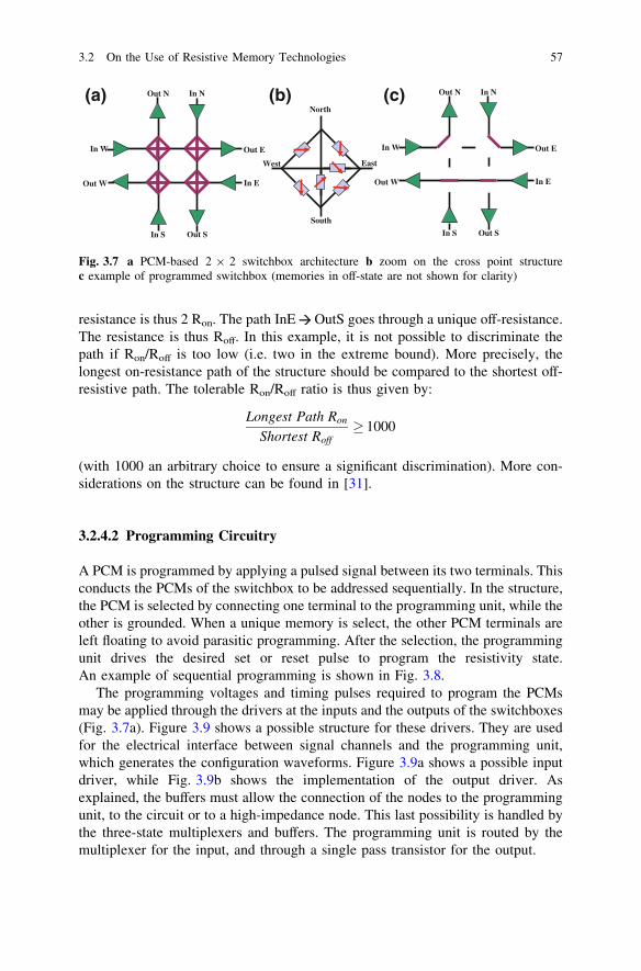
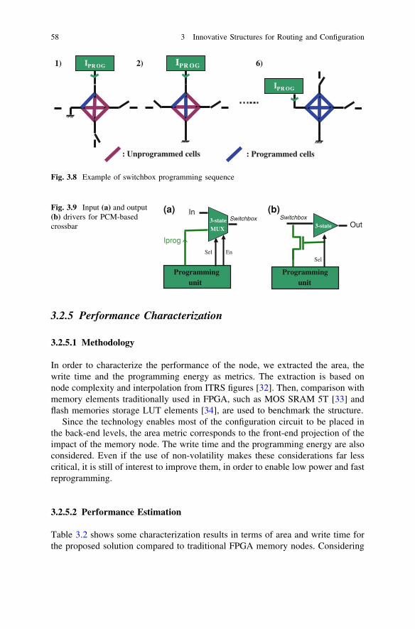

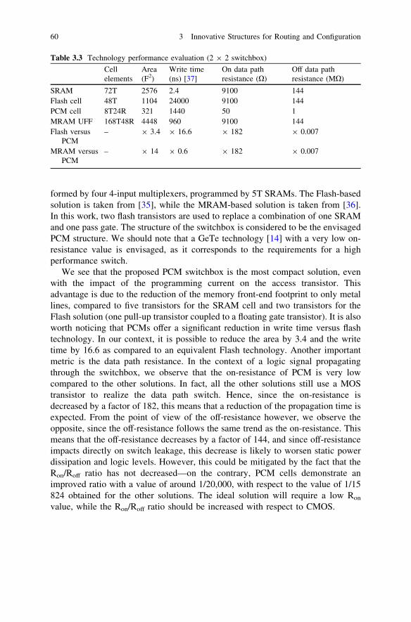


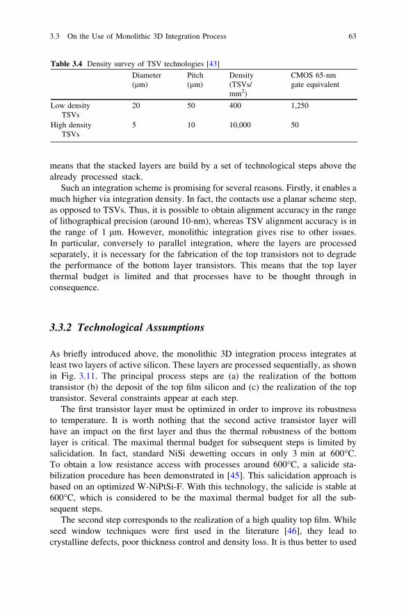

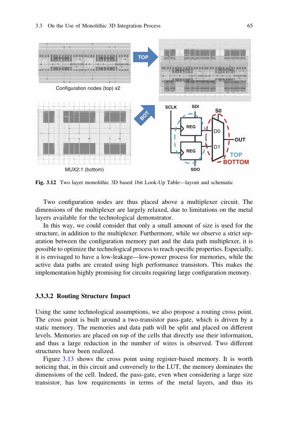

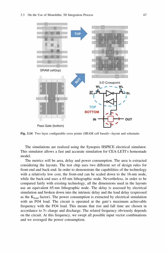


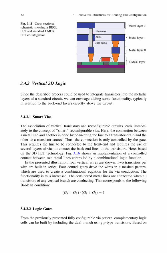
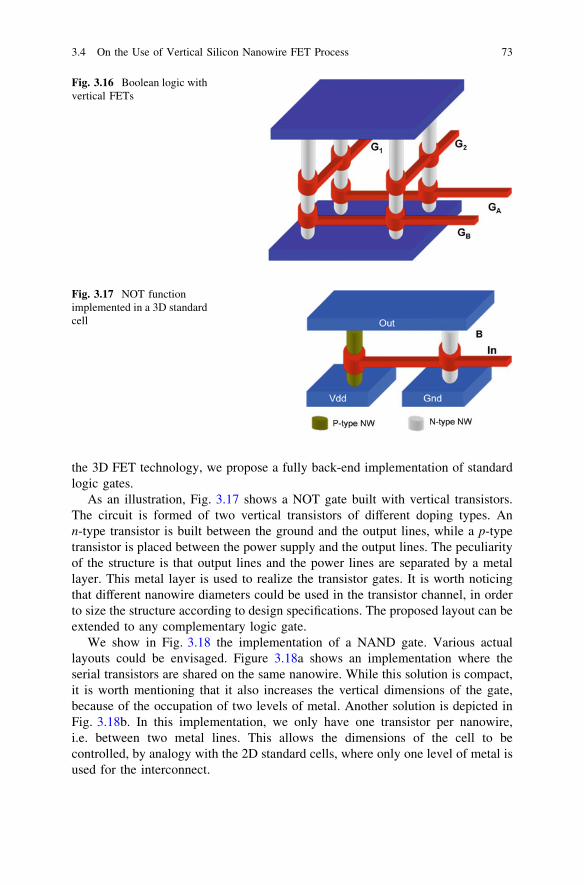
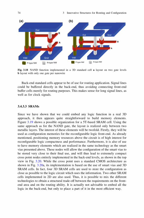
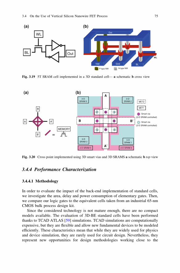
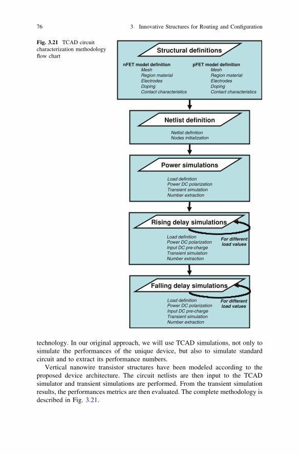


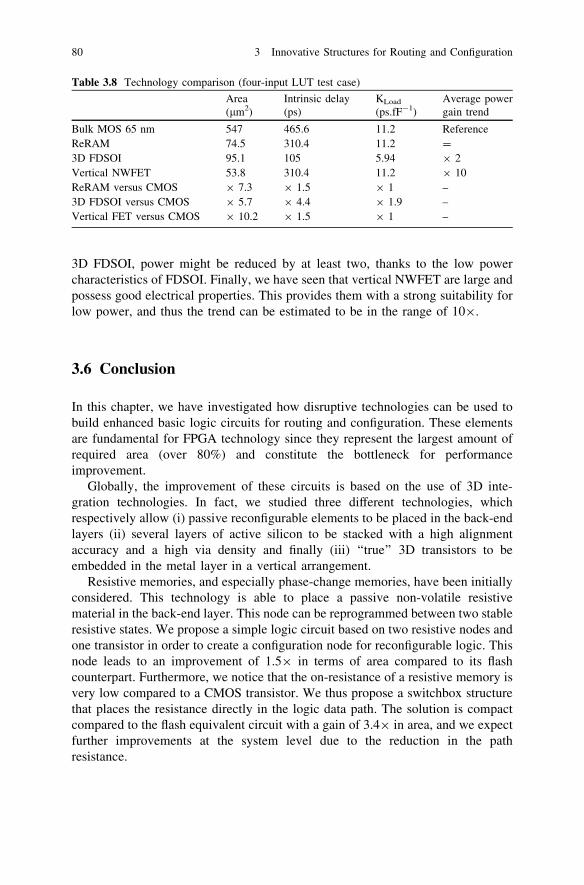


![IP Router Architectures: An Overview - Computer cs757/papers/ Router Architectures: An Overview by James Aweya ... To achieve wire-speed routing, ... switching routing techniques such as IP Switching [1], ...](https://static.documents.pub/doc/80x56/5a9971ef7f8b9a8b5d8dfdcc/ip-router-architectures-an-overview-computer-cs757papersawey99pdfip-router.jpg)


