Page 1
i
A
Project Report
On
Design and Implementation Of
Fast Fourier Transform and Inverse Fast Fourier
Transform On FPGA
Submitted to
Rajiv Gandhi Technical University, Bhopal, Madhya Pradesh,
India.
in partial fulfillment of the requirement for the award of the degree of
Bachelor of Engineering (Electronics and Communication)
By
Abhijay Singh Sisodia (0905EC051002)
Under the Guidance of
Mr. Vineet Shrivastava
at
Department of Electronics and Communication
Institute of Technology and Management, Gwalior, Madhya Pradesh.
Page 2
ii
INSTITUTE OF TECHNOLOGY AND MANAGEMENT
GWALIOR, INDIA.
Certificate
I hereby certify that the work which is being presented in the major project entitled “Design
and Implementation of Fast Fourier Transform and Inverse Fast Fourier Transform on
FPGA” in partial fulfillment of the requirement for the award of the degree of Bachelor of
Engineering (Electronics and Communication) at Institute of Technology and
Management, Gwalior is an authentic record of my own work carried out under the
supervision of undersign and refers others researchers‘ work which are duly listed in the
reference section.
The matter embodied in this work has not been submitted for the award of any other degree
of this or any other university.
Abhijay Singh Sisodia (0905EC051002)
This is to certify that the above statement made by the candidate is correct and true to the
best of my knowledge.
Mr. Vineet Shrivastava
Assistant Professor, Department of Electronics and Communication
Mrs. R. A. Bhatia Dr.. Y.M. Gupta
Associate Professor and Head of the Department Director
Department of Electronics and Communication
Page 3
iii
Abstract
The objective of this project is to design and implement Fast Fourier Transform (FFT) and
Inverse Fast Fourier Transform (IFFT) module on a FPGA hardware. This project
concentrates on developing FFT and IFFT. The work includes in designing and mapping of
the module. The design uses 8-point FFT and IFFT for the processing module which indicate
that the processing block contain 8 inputs data. The Fast Fourier Transform and Inverse Fast
Fourier Transform are derived from the main function which is called Discrete Fourier
Transform (DFT). The idea of using FFT/IFFT instead of DFT is that the computation of the
function can be made faster where this is the main criteria for implementation in the digital
signal processing. In DFT the computation for N-point of the DFT will calculate one by one
for each point. While for FFT/IFFT, the computation is done simultaneously and this method
saves quite a lot of time. The project uses radix-2 DIF-FFT algorithm breaks the entire DFT
calculation down into a number of 2-point DFTs. Each 2-point DFT consists of a multiply-
and-accumulate operation called a butterfly,
All modules are designed using VHDL programming language and implement using FPGA
board. The board is connected to computer through serial port and development kit software
is used to provide interface between user and the hardware. All processing is executed in
FPGA board and user only requires to give the inputs data to the hardware through software.
Input and output data is displayed to computer and the results is compared using simulation
software. The design process and downloading process into FPGA board uses VHDL and the
same is used to execute the designed module.
Page 4
iv
List of Figures
Figure 2.1 Fourier Transform Family
Figure 2.2 Application of DFT
Figure 2.3: Comparison between Real and Complex Transform
Figure 2.4: Conversion between polar and rectangular Co-ordinates
Figure 2.5 Values of Twiddle Factor
Figure3.1: The butterfly computation in DIT-FFT
Figure 3.2: 8- point DIT FFT algorithm
Figure 3.3 DIT-FFT Signal Flow Graph
Figure 3.4: Bit reversal Example
Figure 3.5: DIF-FFT butterfly structure
Figure 3.6 DIF-FFT algorithms
Figure 3.7 –Point DIF-FFT Signal Flow Graph using Decimation in Frequency (DIF)
Figure 4.1: FPGA Architecture
Figure 4.2: FPGA Configurable Logic Block [25]
Figure 4.3: FPGA Configurable I/O Block
Figure 4.4: FPGA Programmable Interconnect
Figure 4.5: FPGA Design Flow
Figure 4.6: Top-Down Design
Figure 4.7: Asynchronous: Race Condition
Figure 4.8: Synchronous: No Race Condition
Figure 4.9: Asynchronous: Delay Dependent Logic
Figure 4.10: Synchronous: Delay Independent Logic
Figure 4.11: Asynchronous: Hold Time Violation
Figure 4.12: Asynchronous: Glitch
Figure 4.13: Synchronous: No Glitch
Figure 4.14: Asynchronous: Bad Clocking
Page 5
v
Figure 4.15: Synchronous: Good Clocking
Figure 4.16: Metastability - The Problem
Figure 5.1: Mapping Module
Figure 5.2: FFT module
Figure 6.1: R-S Flip-Flop
Figure 6.2: A clock wave form with constant on–off period
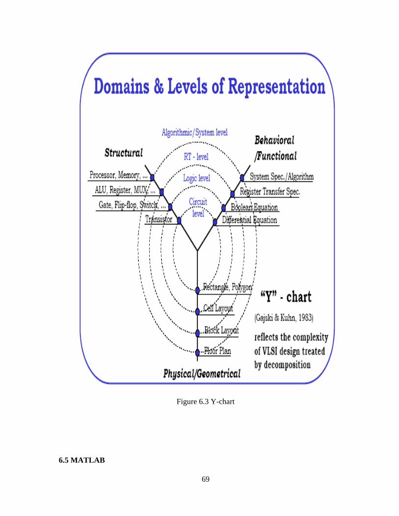
Figure 6.3: Y-chart
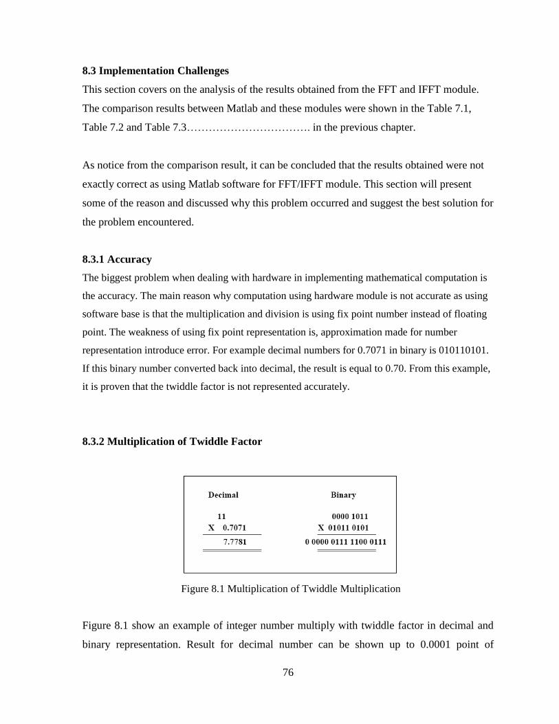
Figure 8.1: Multiplication of Twiddle Multiplication
Figure 8.2: Example of twiddle multiplication
Figure 8.3: Addition of decimal number
Page 6
vi
Dedicated to
My mother, father, faculty, family and friends.
Page 7
vii
Table of Contents
CHAPTER PAGE NUMBER
Certificate i
Acknowledgements ii
Abstract iii
List of Figures iv-v
1. Introduction 12-14
1.1 Motivation 1
1.2 Objective 2
2. Discrete Fourier Transform 15-23
2.1 Introduction 4
2.2 Brief History 8
2.3 Fundamentals of Fast Fourier Transform (FFT) Algorithm 9
2.3 Classification 10
2.3.1 On the basis of storage of component 10
2.3.1.1 In-Place FFT algorithm 10
2.3.1.2 Natural Input-Output FFT algorithm 11
2.3.2 On the basis of decimation process 11
2.3.2.1 Decimation-in Time FFT algorithm 11
2.3.2.1 Decimation-in Frequency FFT algorithm 11
2.4 Comparison of direct computation of DFT and by FFT algorithm 12
3. Fast Fourier Transform (FFT) 13-33
3.1 Decimation-in time FFT algorithm 13
3.2 Decimation-in frequency FFT algorithm 17
3.2.1 Steps for computation of DIF-FFT 18
vii
Page 8
viii
3.4 Inverse Fast Fourier Transform(IFFT) 20
3.5 Classification of architecture 21
4. Introduction to FPGA Design 23-42
4.1 Field Programmable Gate Array (FPGA) 23
4.2 FPGA Architecture 23
4.3 Configurable Logic Blocks 24
4.4 Configurable I/O Blocks 25
4.5 Programmable Interconnect 25
4.6 Clock Circuitry 26
4.7 Small v/s Large Granularity 27
4.8 SRAM v/s Anti-fuse Programming 27
4.9 Example of FPGA Families 28
4.10 The Design Flow 28
4.11 Writing a Specification 30
4.11.1 Choosing a Technology 30
4.11.2 Choosing a Design Entry Method 31
4.11.3 Choosing a Synthesis tool 31
4.11.4 Designing a Chip 31
4.11.5 Simulating – Design Review 32
4.11.6 Synthesis 32
4.11.7 Place and Route 32
4.11.8 Re-simulating – Final Review 32
4.11.9 Testing 33
4.12 Design Issues 33
4.12.1 Top-Down Design 33
4.12.2 Keep the Architecture in Mind 34
4.12.3 Synchronous Design 35
4.13 Race Conditions 35
4.14 Delay Dependent Logic 36
4.15 Hold Time violations 37
4.16 Glitches 38
4.17 Bad Clocking 39
Page 9
ix
4.18 Metastability 40
4.19 Timing Simulation 42
5. System Implementation 44-47
5.1 Introduction 44
5.2 Design Considerations 44
5.3 Implementation 46
5.4 Hardware Modules 47
5.4.1 FFT module 47
5.4.2 IFFT module 47
6. Design Walkthrough 48-73
6.1 Introduction 48
6.2 Review study topics 48
6.3 Design Process 49
6.4 Description of VHDL 52
6.4.1 VHDL Terminology 52
6.4.2 Superceding traditional Design Methods 57
6.4.3 Symbol Vs Entity 60
6.4.4 Schematic and Architecture 60
6.4.5 VHDL Design Process 61
6.4.6 VHDL test – Bench and Verification 62
6.4.7 VHDL Modeling 62
6.4.7.1 Structural Style of Modeling 62
6.4.7.2 Data Flow Style of Modeling 64
6.4.7.3 Behavioral Style of Modeling 66
6.4.7.4 Mixed Style of Modeling 69
6.4.7.1 State Machine Modeling 71
6.5 MATLAB 73
Page 10
x
7. Result and Simulation 74-77
8. Conclusion and Challenges 78-81
8.1 Design Solution 78
8.2 Suggestion for Future Research 78
8.3 Implementation Challenges 79
8.3.1 Accuracy 79
8.3.2 Multiplication by Twiddle factor 80
8.3.3 Division by eight 81
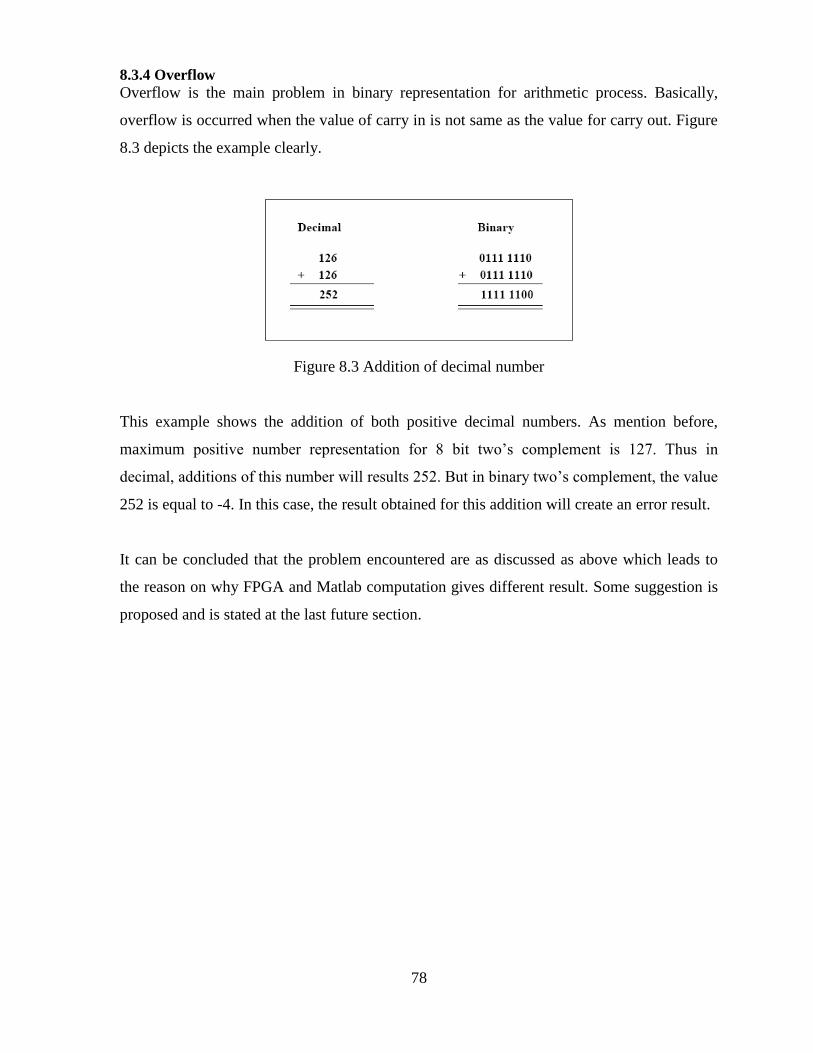
8.3.4 Overflow 81
References 82-83
Page 12
1
CHAPTER 1
INTRODUCTION
1.1 Motivation
This chapter covers the material on project background, project objectives, project scope and
the project outline. Introduction on this chapter covers about the FFT/IFFT implementation
method and description on the available hardware for implementation. The problem
statement of the project will also be carried out in this chapter.
With the rapid growth of digital communication in recent years, the need for high-speed data
transmission has been increased. The mobile telecommunications industry faces the problem
of providing the technology that be able to support a variety of services ranging from voice
communication with a bit rate of a few kbps to wireless multimedia in which bit rate up to 2
Mbps. Many systems have been proposed and FFT/IFFT system has gained much attention
for different reasons. Although DFT (Discrete Fourier Transform) was first developed in the
1960s, only in recent years, it has been recognized as an outstanding method for high-speed
cellular data communication where its implementation relies on very high-speed digital
signal processing. This method has only recently become available with reasonable prices
versus performance of hardware implementation.
Since DFT is carried out in the digital domain, there are several methods to implement the
system. One of the methods to implement the system is using ASIC (Application Specific
Integrated Circuit). ASICs are the fastest, smallest, and lowest power way to implement DFT
into hardware. The main problem using this method is inflexibility of design process
involved and the longer time to market period for the designed chip.
Another method that can be used to implement DFT is general purpose Microprocessor or
Micro Controller. Power PC 7400 and DSP Processor is an example of microprocessor that is
capable to implement fast vector operations. This processor is highly programmable and
flexible in term of changing the DFT design into the system. The disadvantages of using this
hardware are, it needs memory and other peripheral chips to support the operation. Beside
Page 13
2
that, it uses the most power usage and memory space, and would be the slowest in term of
time to produce the output compared to other hardware.
Field-Programmable Gate Array (FPGA) is an example of VLSI circuit which consists of a
―sea of NAND gates‖ whereby the function are customer provided in a ―wire list‖. This
hardware is programmable and the designer has full control over the actual design
implementation without the need (and delay) for any physical IC fabrication facility. An
FPGA combines the speed, power, and density attributes of an ASIC with the
programmability of a general purpose processor will give advantages to the FFT/IFFT
system. An FPGA could be reprogrammed for new functions by a base station to meet future
needs particularly when new design is going to fabricate into chip. This will be the best
choice for FFT/IFFT implementation since it gives flexibility to the program design besides
the low cost hardware component compared to others.
1.2 Objective
The aim for this project is to design a module for FFT (Fast Fourier Transform) and IFFT
(Inverse Fast Fourier Transform), mapping (modulator), using hardware programming
language (VHDL). These designs were developed using VHDL programming language in
design entry software. The design is then implemented in the FPGA development board.
Description on the development board will be carried out at methodology chapter.
In order to implement IFFT computation in the FPGA hardware, the knowledge on Very
High Speed Integrated Circuit (VHSIC) Hardware Description Language (VHDL)
programming is required. This is because FPGA chip is programmed using VHDL language
where the core block diagram of the FFT/IFFT implements in this hardware. The transmitter
and receiver are developed in one FPGA board, thus required both IFFT and FFT algorithm
implemented in the system.
The works involved is focused on the design of the core processing block using 8 point Fast
Fourier Transform (FFT) for receiver and 8 point Inverse Fast Fourier Transform (IFFT) for
transmitter part. The implementation of this design into FPGA hardware is to no avail for
several reasons encountered during the integration process from software into FPGA
hardware.
Page 14
3
The project was done up to simulation level using Model Sim software and only consists FFT
and IFFT processing module. Some of the problem encountered by during project was that
the design of FFT and IFFT is not fit to FPGA hardware. The design used a large number of
gates and causes this problem to arise. Logic gates are greatly consumed if the number of
multiplier and divider are increase. One method to overcome this problem is by decreasing
the number of multiplier and divider in the VHDL design.
Beside that, the design does not include control signal which cause difficulties in controlling
the data processing in FFT or IFFT module. The control signal is use to select the process
executed for each computation process during VHDL design. As a result, the design is not
applicable for hardware implementation in the FPGA development board. New design is
required to overcome this problem. Since the design is not possible to use, this project will
concentrate on designing the FFT and IFFT module which can be implement in the dedicated
FPGA board. To ensure that the program can be implemented, the number of gates used in
the design must be small or at least less than the hardware can support. Otherwise the design
module is not able to implement into the dedicated board.
The work of the project will be focused on the design of the processing block which is 8
point IFFT and FFT function. The design also includes mapping block, serial to parallel and
parallel to serial block set. All design need to be verified to ensure that no error in VHDL
programming before being simulated. Design process will be described on the methodology
chapter.
The second scope is to implement the design into FPGA hardware development board. This
process is implemented if all designs are correctly verified and simulated using particular
software. Implementation includes hardware programming on FPGA or downloading
hardware design into FPGA and software programming.
CHAPTER II
DISCRETE FOURIER TRANSFORM
Page 15
4
2.1 Introduction
With the rapid growth of digital communication in recent years, the need for high-speed data
transmission has increased. The mobile telecommunications industry faces the problem of
providing the technology that be able to support a variety of services ranging from voice
communication with a bit rate of a few kbps to wireless multimedia in which bit rate up to 2
Mbps. Many systems have been proposed and FFT/IFFT based system has gained much
attention for different reasons. Although FFT/IFFT was first developed in the 1960s, only
recently has it been recognized as an outstanding method for high-speed cellular data
communication where its implementation relies on very high-speed digital signal processing,
and this has only recently become available with reasonable prices of hardware
implementation.
Fourier analysis forms the basis for much of digital signal processing. Simply stated, the
Fourier transform (there are actually several members of this family) allows a time domain
signal to be converted into its equivalent representation in the frequency domain. Conversely,
if the frequency response of a signal is known, the inverse Fourier transform allows the
corresponding time domain signal to be determined.
In addition to frequency analysis, these transforms are useful in filter design, since the
frequency response of a filter can be obtained by taking the Fourier transform of its impulse
response. Conversely, if the frequency response is specified, then the required impulse
response can be obtained by taking the inverse Fourier transform of the frequency response.
Digital filters can be constructed based on their impulse response, because the coefficients of
an FIR filter and its impulse response are identical.
The Fourier transform family (Fourier Transform, Fourier Series, Discrete Time Fourier
Series, and Discrete Fourier Transform) is shown in Figure 2.1. These accepted definitions
have evolved (not necessarily logically) over the years and depend upon whether the signal is
continuous–aperiodic, continuous–periodic, sampled–aperiodic, or sampled–periodic. In this
context, the term sampled is the same as discrete (i.e., a discrete number of time samples).
Page 16
5
Figure 2.1 Fourier Transform Family
The only member of this family which is relevant to digital signal processing is the Discrete
Fourier Transform (DFT) which operates on a sampled time domain signal which is
periodic. The signal must be periodic in order to be decomposed into the summation of
sinusoids. However, only a finite number of samples (N) are available for inputting into the
DFT. This dilemma is overcome by placing an infinite number of groups of the same N
samples ―end-to-end,‖ thereby forcing mathematical (but not real-world) periodicity as
shown in Figure 2.1.
The basic function of DFT can be exemplified by the following figure2.2.
Figure 2.2 Application of DFT
The fundamental analysis equation for obtaining the N-point DFT is as follows:
There are two basic types of DFTs: real, and complex. The complex DFT, is where the input
and output are both complex numbers. Since time domain input samples are real and have no
imaginary part, the imaginary part of the input is always set to zero. The output of the DFT,
X(k), contains a real and imaginary component which can be converted into amplitude and
phase.
Page 17
6
The real DFT, although somewhat simpler, is basically a simplification of the complex DFT.
Most FFT routines are written using the complex DFT format, therefore understanding the
complex DFT and how it relates to the real DFT is important. For instance, if you know the
real DFT frequency outputs and want to use a complex inverse DFT to calculate the time
samples, you need to know how to place the real DFT outputs points into the complex DFT
format before taking the complex inverse DFT. Notice that the cosine and sine terms in the
equation can be expressed in either polar or rectangular coordinates using Euler‘s equation:
ejθ
= cos θ + j sin θ
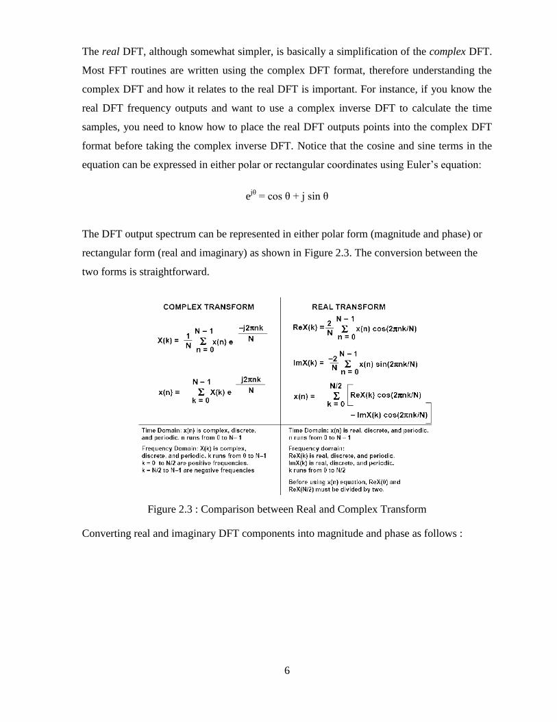
The DFT output spectrum can be represented in either polar form (magnitude and phase) or
rectangular form (real and imaginary) as shown in Figure 2.3. The conversion between the
two forms is straightforward.
Figure 2.3 : Comparison between Real and Complex Transform
Converting real and imaginary DFT components into magnitude and phase as follows :
Page 18
7
Figure 2.4 : Conversion between polar and rectangular Co-ordinates
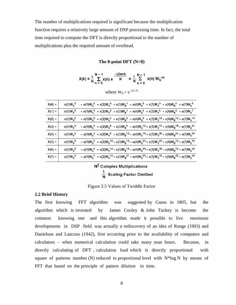
In order to understand the development of the FFT, consider first the 8-point DFT
expansion shown in Figure 5.10. In order to simplify the diagram, note that the
quantity WN is defined as:
WN = e−j2π /N
.
This leads to the definition of the twiddle factors as:
WNnk
= e−j2πnk /N
.
Table 2.1: Twiddle Factor value for FFT
FFT (N=8)
nk W Value
1 W80 1
2 W81 .07071-.7071j
3 W82 -j1
4 W83 -.07071-.7071j
5 W84 1
6 W85 -.07071+.7071j
7 W86 j1
8 W87 .07071+.7071j
The twiddle factors are simply the sine and cosine basis functions written in polar
form. Note that the 8-point DFT shown in the diagram requires 64 complex
multiplications. In general, an N-point DFT requires N2 complex multiplications.
Page 19
8
The number of multiplications required is significant because the multiplication
function requires a relatively large amount of DSP processing time. In fact, the total
time required to compute the DFT is directly proportional to the number of
multiplications plus the required amount of overhead.
The 8-point DFT (N=8)
where WN = e−j2π /N
Figure 2.5 Values of Twiddle Factor
2.2 Brief History
The first knowing FFT algorithm was suggested by Gauss in 1805, but the
algorithm which is invented by James Cooley & John Tuckey is become the
common knowing one and this algorithm made it possible to live enormous
developments in DSP field. was actually a rediscovery of an idea of Runge (1903) and
Danielson and Lanczos (1942), first occurring prior to the availability of computers and
calculators – when numerical calculation could take many man hours. Because, in
directly calculating of DFT , calculation load which is directly proportional with
square of patterns number (N) reduced to proportional level with N*log N by means of
FFT that based on the principle of pattern dilution in time.
Page 20
9
In 1971, Weinstein and Ebert made an important contribution. Discrete Fourier transform
(DFT) method was proposed to perform the base band modulation and demodulation. DFT is
an efficient signal processing algorithm. It eliminates the banks of sub carrier oscillators.
They used guard space between symbols to combat ICI and ISI problem.
Originally, multi-carrier systems were implemented through the use of separate local
oscillators to generate each individual sub carrier. This was both efficient and costly. With
the advent of cheap powerful processors, the sub-carriers can now be generated using Fast
Fourier Transform (FFT). The FFT is used to calculate the spectral content of the signal. It
moves a signal from the time domain where it is expressed as a series of time events to the
frequency domain where it is expressed as the amplitude and phase of a particular frequency.
The inverse FFT (IFFT) performs the reciprocal operation.
2.2 Fundamentals (FFT) Algorithm
The FFT is simply an algorithm to speed up the DFT calculation by reducing the number of
multiplications and additions required. In order to understand the basic concepts of the FFT
and its derivation, note that the DFT expansion can be greatly simplified by taking advantage
of the symmetry and periodicity of the twiddle factors as shown in Figure 2.5. If the
equations are rearranged and factored, the result is the Fast Fourier Transform (FFT) which
requires only (N/2) log2(N) complex multiplications. The computational efficiency of the
FFT versus the DFT becomes highly significant when the FFT point size increases to several
thousand as shown in Table 2.3.However, notice that the FFT computes all the output
frequency components (either all or none!). If only a few spectral points need to be
calculated, the DFT may actually be more efficient. Calculation of a single spectral output
using the DFT requires only N complex multiplications.
Direct computation of the DFT is less efficient because it does not exploit the properties of
symmetry and periodicity of the phase factor WN=e-j2∏/N
.
Symmetry property : WNK+N/2
= -WNK
Periodicity property : WNK+N
= WNK
Table 2.1
Page 21
10
2.3 Classification
2.3.1 On the basis of storage of component
According to the storage of the component of the intermediate vector, FFT algorithms are
classified into two groups.
2.3.1.1 In-Place FFT algorithm
In this FFT algorithm, component of an intermediate vector can be stored at the same place as
the corresponding component of the previous vector.
In-place FFT algorithm reduce the memory space requirement.
2.3.1.2 Natural Input-Output FFT algorithm
In this FFT algorithm, both input and output are in natural order . it means that both discrete
time sequence s(n) and its DFT S(K) are in natural order. This type of algorithm consumes
more memory space for preservation of natural order of s(n) and S(K).
The disadvantage of an in-place FFT algorithm is that the output appears in an unnatural
order necessitating proper shuffling of s(n) or S(K).This shuffling is known as Scrambling.
2.3.2 On the basis of decimation process
Page 22
11
Classification of FFT algorithm based on Decimation of s(n) or S(K).Decimation means
decomposition into decimal parts.
In Radix-2 FFT of N points –where N is integer power of 2- requires N log2N complex
operations compared to N2 of direct DFT computation. Also, algorithms are known in two
types DIT, decimation in time, where complex multiplication occurs after the two-point DFT;
and DIF, decimation in frequency, where complex multiplication occurs before the two-point
DFT. Further more, the notations ―in-place‖ and ―not-in-place‖ refer whether an input point
ends up in the same register it came from or not. The FFT algorithm consists of log2N stages.
Each stage consists of N/2 radix-2 butterfly operations
2.3.2.1 Decimation-in Time FFT algorithm
In DIT FFT algorithms the sequence s(n) will be broken up into odd numbered and even
numbered subsequences. As mentioned above, this algorithm was first proposed by Cooley
and Tukey in 1965.
2.3.2.2 Decimation-in frequency FFT algorithm
In DIF-FFT the sequence s(n) will be broken up into two equal halves. This algorithm was
first proposed by Gentlemen and Sande in 1966.
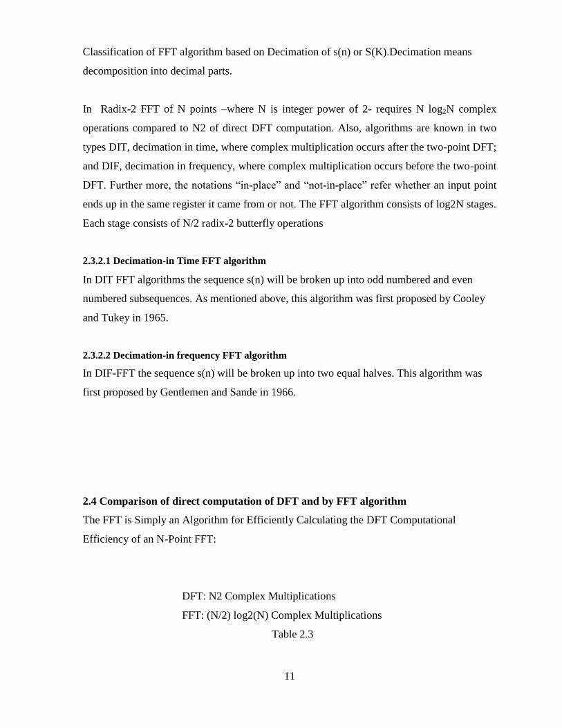
2.4 Comparison of direct computation of DFT and by FFT algorithm
The FFT is Simply an Algorithm for Efficiently Calculating the DFT Computational
Efficiency of an N-Point FFT:
DFT: N2 Complex Multiplications
FFT: (N/2) log2(N) Complex Multiplications
Table 2.3
Page 23
12
CHAPTER III
FAST FOURIER TRANSFORM
Before going further to discus on the FFT and IFFT design, it is good to explain a bit on the
Fast Fourier Transform and Inverse Fast Fourier Transform operation. The Fast Fourier
Transform (FFT) and Inverse Fast Fourier Transform (IFFT) are derived from the main
function which is called Discrete Fourier Transform (DFT). The idea of using FFT/IFFT
instead of DFT is that the computation of the function can be made faster where this is the
main criteria for implementation in the digital signal processing. In DFT the computation for
Page 24
13
N-point of the DFT will calculate one by one for each point. While for FFT/IFFT, the
computation is done simultaneously and this method saves quite a lot of time. Below is the
equation showing the DFT and from here the equation is derived to get FFT/IFFT function.
X (k) = Σ x (n) e -j2∏k/n
3.1 Decimation-in Time FFT algorithm
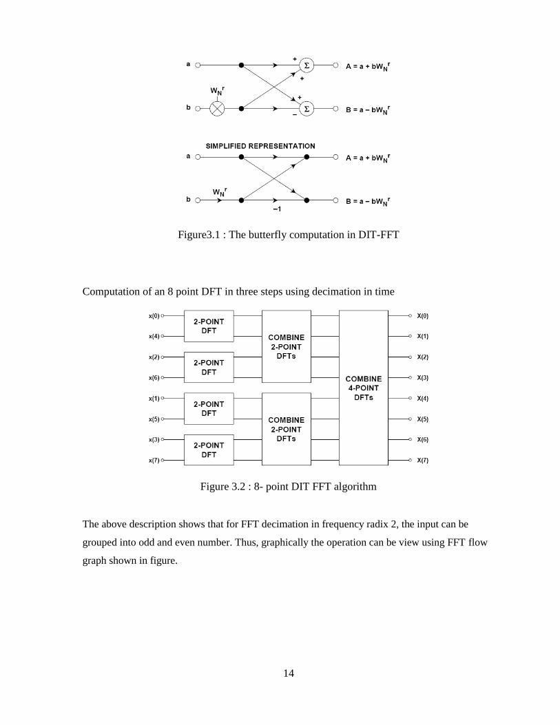
The radix-2 FFT algorithm breaks the entire DFT calculation down into a number of 2-point
DFTs. Each 2-point DFT consists of a multiply-and-accumulate operation called a butterfly,
as shown in Figure 3.1. Two representations of the butterfly are shown in the diagram: the
top diagram is the actual functional representation of the butterfly showing the digital
multipliers and adders. In the simplified bottom diagram, the multiplications are indicated by
placing the multiplier over an arrow, and addition is indicated whenever two arrows converge
at a dot.
The 8-point decimation-in-time (DIT) FFT algorithm computes the final output in three
stages as shown in Figure 3.2. The eight input time samples are first divided (or decimated)
into four groups of 2-point DFTs. The four 2-point DFTs are then combined into two 4-point
DFTs. The two 4-point DFTs are then combined to produce the final output X(k). The
detailed process is shown in Figure 3.3, where all the multiplications and additions are
shown. Note that the basic two-point DFT butterfly operation forms the basis for all
computation. The computation is done in three stages. After the first stage computation is
complete, there is no need to store any previous results. The first stage outputs can be stored
in the same registers which originally held the time samples x(n). Similarly, when the second
stage computation is completed, the results of the first stage computation can be deleted. In
this way, in-place computation proceeds to the final stage. Note that in order for the
algorithm to work properly, the order of the input time samples, x(n), must be properly re-
ordered using a bit reversal algorithm.
The butterfly computation in DIT-FFT
Page 25
14
Figure3.1 : The butterfly computation in DIT-FFT
Computation of an 8 point DFT in three steps using decimation in time
Figure 3.2 : 8- point DIT FFT algorithm
The above description shows that for FFT decimation in frequency radix 2, the input can be
grouped into odd and even number. Thus, graphically the operation can be view using FFT flow
graph shown in figure.
Page 26
15
Figure 3.3 DIT-FFT Signal Flow Graph
The bit reversal algorithm used to perform this re-ordering is shown in Figure 2.8The
decimal index, n, is converted to its binary equivalent. The binary bits are then placed in
reverse order, and converted back to a decimal number. Bit reversing is often performed in
DSP hardware in the data address generator (DAG), thereby simplifying the software,
reducing overhead, and speeding up the computations. The computation of the FFT using
decimation-in-frequency (DIF) is shown in Figures 2.9 and 2.10. This method requires that
the bit reversal algorithm be applied to the output X(k). Note that the butterfly for the DIF
algorithm differs slightly from the decimation-in-time butterfly as shown in Figure 2.5.
The use of decimation-in-time versus decimation-in-frequency algorithms is largely a matter
of preference, as either yields the same result. System constraints may make one of the two a
more optimal solution.
It should be noted that the algorithms required to compute the inverse FFT are nearly
identical to those required to compute the FFT, assuming complex FFTs are used. In fact, a
useful method for verifying a complex FFT algorithm consists of first taking the FFT of the
x(n) time samples and then taking the inverse FFT of the X(k). At the end of this process, the
Page 27
16
original time samples, Re x(n), should be obtained and the imaginary part, Im x(n), should be
zero (within the limits of the mathematical round off errors).
Figure 3.4 : Bit reversal Example
3.2 Decimation-in frequency FFT algorithm
The butterfly computation in DIF-FFT
Figure 3.5 : DIF-FFT butterfly structure
An 8- point DIF FFT algorithm
Page 28
17
Figure 3.6 DIF-FFT algorithm
The equation above shows that for FFT decimation in frequency radix 2, the input can be
grouped into odd and even number. Thus, graphically the operation can be view using FFT flow
graph shown in figure.
Computation of an 8 point DFT in three steps using decimation in frequency
Figure 3.7 –Point DIF-FFT Signal Flow Graph using Decimation in Frequency (DIF)
3.2.1 Steps for computation of DIF-FFT
From this figure, the FFT computation is accomplished in three stages. The X(0) until X(7)
variable is denoted as the input value for FFT computation and Y(0) until Y(7) is denoted as
Page 29
18
the output. There are two operations to complete the computation in each stage. The upward
arrow will execute addition operation while downward arrow will execute subtraction
operation. The subtracted value is multiplied with twiddle factor value before being
processed into the nest stage. This operation is done concurrently and is known as ―butterfly
process‖. For second stage, there are two butterfly process with each process get reduced
input variable. In the first stage the butterfly process get eight input variable while in the
second stage, each butterfly process get four input variable that is from first stage
computation. This process is continued until third stage. In third stage, there are four
butterfly processes. Noted that each of the butterfly process is performed concurrently enable
it to execute FFT computation process in a very fast technique.
Mathematically, the butterfly process for each stage can be derived as the equation stated below.
FFT Stage 1
X(0) + X(4) => X‘(0),
X(1) + X(5) => X‘(1),
X(2) + X(6) => X‘(2),
X(3) + X(7) => X‘(3),
[X(0) – X(4)]W0 => X‘(4),
[X(1) – X(5)]W1 => X‘(5),
[X(2) – X(6)]W2 => X‘(6),
[X(3) – X(7)]W3 => X‘(7),
FFT Stage 2
X‘(0) + X‘(2) => X‖(0),
X‘(1) + X(3) => X‖(1),
[X‘(0) – X‘(2)]W0 => X‖(2),
[X‘(1) – X‘(3)]W0 => X‖(3),
X‘(4) + X‘(2) => X‖(4),
X‘(5) + X(3) => X‖(5),
[X‘(4) – X‘(6)]W0 => X‖(6),
[X‘(5) – X‘(7)]W0 => X‖(7),
FFT Stage 3
Page 30
19
X‖(0) + X‖(1) => Y(0),
X‖(1) – X‖(5) => Y(1),
X‖(2) + X‖(3) => Y(2),
X‖(2) – X‖(3) => Y(3),
X‖(4) + X‖(5) => Y(4),
X‖(4) – X‖(5) => Y(5),
X‖(6) + X‖(7) => Y(6),
X‖(6) – X‖(7) => Y(7),
The FFTs discussed up to this point are radix-2 FFTs, i.e., the computations are based on 2-
point butterflies. This implies that the number of points in the FFT must be a power of 2. If
the number of points in an FFT is a power of 4, however, the FFT can be broken down into a
number of 4-point DFTs as shown in Figure 5.20. This is called a radix-4 FFT. The
fundamental decimation-in-time butterfly for the radix-4 FFT is shown in Figure 5.21.
The radix-4 FFT requires fewer complex multiplications but more additions than the radix-2
FFT for the same number of points. Compared to the radix-2 FFT, the radix-4 FFT trades
more complex data addressing and twiddle factors with less computation. The resulting
savings in computation time varies between different DSPs but a radix-4 FFT can be as much
as twice as fast as a radix-2 FFT for DSPs with optimal architectures.
3.4 Inverse Fast Fourier Transform
In Inverse Fast Fourier Transform (IFFT) , the data bits is represent as the frequency domain
and since IFFT convert signal from frequency domain to time domain, it is used in
transmitter to handle the process. IFFT is defined as the equation below.
x(n) = (1/N) Σ X (n) w -nk
Comparing this with the first equation, it is shown that the same FFT algorithm can be used
to find the IFFT function with some changes in certain properties. The changes that
implement is by adding a scaling factor of 1/N and replacing twiddle factor value (Wnk
) with
the complex conjugate W−nk
to the equation (1) of FFT. With these changes, the same FFT
Page 31
20
flow graph also can be used for the Inverse fast Fourier Transform. Below is the table show
the value of twiddle factor for IFFT
Table 3.1 : Twiddle factor for 8 point Inverse Fast Fourier Transform
IFFT (N=8)
nk W Value
1 W8-0
1
2 W8-1
.07071+.7071j
3 W8-2
j1
4 W8-3
-.07071+.7071j
5 W8-4
-1
6 W8-5
-.07071-.7071j
7 W8-6
-j1
8 W8-7
.07071-.7071j
The equation above shows that for FFT decimation in frequency radix 2, the input can be
grouped into odd and even number. Thus, graphically the operation can be view using FFT
flow graph shown in figure.
3.5 Architecture Classification
The Fast Fourier Transform (FFT) is a conventional method for an accelerated computation
of the Discrete Fourier Transform (DFT), which has been used in many applications such as
spectrum estimation, fast convolution and correlation, signal modulation, etc. Even though
FFT algorithmically improves computational efficiency, additional hardware-based
accelerators are used to further accelerate the processing through parallel processing
techniques. A variety of architectures have been proposed to increase the speed, reduce the
power consumption, etc.
A single memory architecture consists of a scalar processor connected to a single N-word
memory via a bidirectional bus. While this architecture is simple, its performance suffers
from inefficient memory bandwidth.
Page 32
21
A cache memory architecture adds a cache memory between the processor and the memory
to increase the effective memory bandwidth. Baas, presented a cache FFT algorithm which
increases energy efficiency and effectively lowers the power consumption.
Dual memory architecture, implemented uses two memories connected to a digital array
signal processor. The programmable array controller generates addresses to memories in a
ping-pong fashion.
The processor array architecture, consists of independent processing elements, with local
buffers, which are connected using an interconnect network.
Pipeline FFT architectures, introduced in , contain log r N blocks; each block consists of
delay lines, arithmetic units that implement a radix-r FFT butterfly operation and ROMs for
twiddle factors. A variety of pipeline FFTs have been implemented. Most pipeline FFT
realizations use delay lines for data reordering between the processing elements. Although
this gives simple data flow architecture, it causes high power consumption.
Many of the FFT algorithms relate to the ―butterfly structure‖ presented first by Cooley and
Tukey where separate processing element (PE) is assigned for each node of the FFT flow.
FFT algorithms have several stages of so called butterfly computations, and a number of
butterflies are calculated at each stage. In the pipeline FFT architecture all the butterflies of
each stage are computed using a single PE and PE assigned to different stages form a line of
processors. It is also possible to map the computation network into another line of processing
where the stages of FFT are sequentially computed by parallel PE‘s connected by the perfect
shuffling network. All the butterflies of a single stage are computed in parallel. This is called
iterative architecture.
3.6 Application of FFT/IFFT systems
The usage of Fast Fourier Transforms can be broadly classified in following fields :
Digital Spectral Analysis
Spectrum Analyzers
Speech Analysis
Page 33
22
Imaging
Pattern Recognition
Filter Design
Calculating Impulse response from frequency response
Calculating frequency response from impulse response
For efficient calculation of DFT.
CHAPTER IV
INTRODUCTION TO FPGA DESIGN
4.1 Field Programmable Gate Arrays (FPGA)
Field Programmable Gate Arrays are called this because rather than having a structure
similar to a PAL or other programmable device, they are structured very much like a
gate array ASIC. This makes FPGAs very nice for use in prototyping ASICs, or in places
where and ASIC will eventually be used. For example, an FPGA maybe used in a design
that need to get to market quickly regardless of cost. Later an ASIC can be used in place
of the FPGA when the production volume increases, in order to reduce cost.
4.2. FPGA Architectures:
Page 34
23
Figure 4.1: FPGA Architecture
Each FPGA vendor has its own FPGA architecture, but in general terms they are all a
variation of that shown in Figure 4.1. The architecture consists of configurable logic blocks,
configurable I/O blocks, and programmable interconnect. Also, there will be clock circuitry
for driving the clock signals to each logic block, and additional logic resources such as
ALUs, memory, and decoders may be available. The two basic types of programmable
elements for an FPGA are Static RAM and anti-fuses.
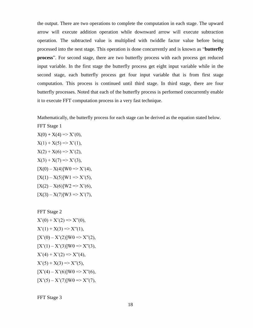
4.3. Configurable Logic Blocks:
Configurable Logic Blocks contain the logic for the FPGA. In large grain
architecture, these CLBs will contain enough logic to create a small state machine. In fine
grain architecture, more like a true gate array ASIC, the CLB will contain only very basic
logic. The diagram in Figure 4.2 would be considered a large grain block. It contains RAM
for creating arbitrary combinatorial logic functions [25]. It also contains flip-flops for
clocked storage elements, and multiplexers in order to route the logic within the block and to
and from external resources. The multiplexers also allow polarity selection and reset and clear
input selection.
Page 35
24
Figure 4.2: FPGA Configurable Logic Block [25]
4.4. Configurable I/O Blocks:
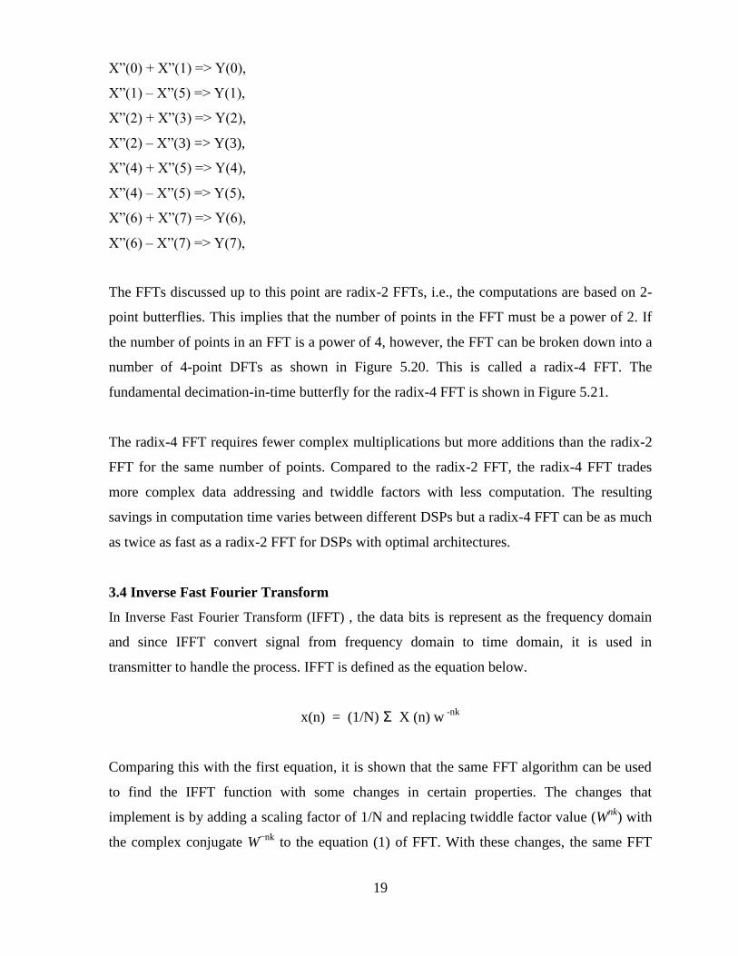
A Configurable I/O Block, shown in Figure 4.3, is used to bring signals onto the chip and
send them back off again. It consists of an input buffer and an output buffer with three
state and open collector output controls. Typically there are pull up resistors on the
outputs and sometimes pull down resistors. The polarity of the output can usually be
programmed for active high or active low output and often the slew rate of the output can
be programmed for fast or slow rise and fall times. In addition, there is often a flip-
flop on outputs so that clocked signals can be output directly to the pins without
encountering significant delay. It is done for inputs so that there is not much delay on a
signal before reaching a flip-flop which would increase the device hold time requirement.
Page 36
25
Figure 4.3: FPGA Configurable I/O Block
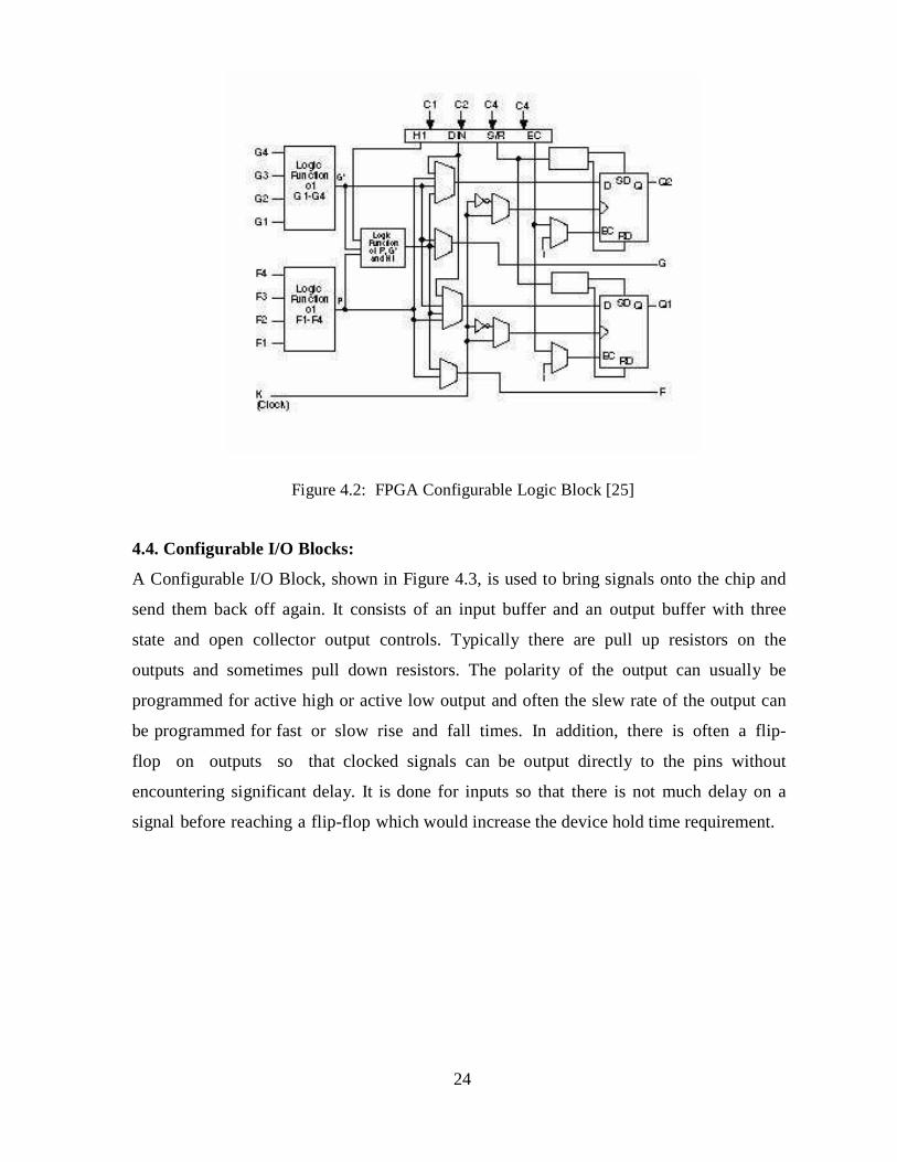
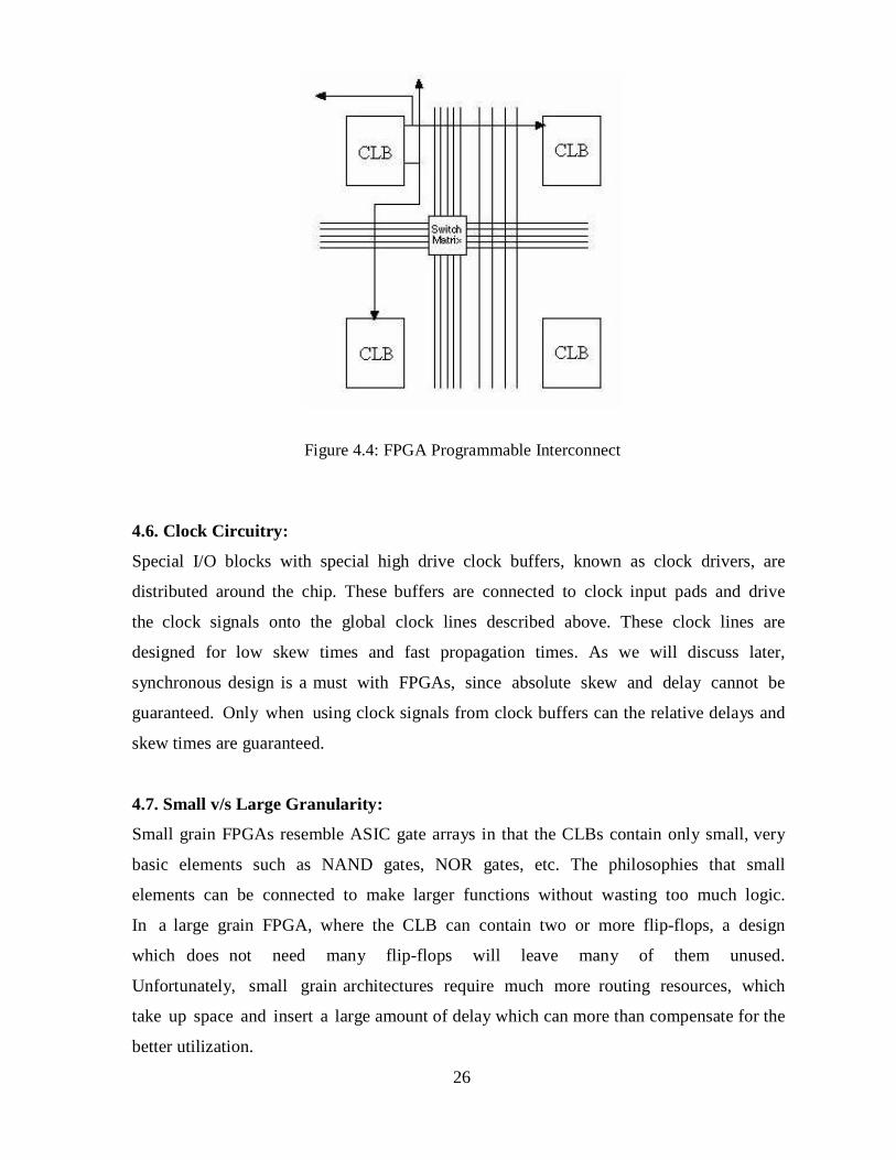
4.5. Programmable Interconnect:
Interconnect of an FPGA is very different than that of a CPLD, but is rather similar to that
of a gate array ASIC. In Figure 4.4, a hierarchy of interconnect resources can be seen.
There are long lines which can be used to connect critical CLBs that are physically far
from each other on the chip without inducing much delay. They can also be used as
buses within the chip. There are also short lines which are used to connect individual
CLBs which are located physically close to each other. There are often one or several
switch matrices, like that in a CPLD, to connect these long and short lines
together in specific ways. Programmable switches inside the chip allow the connection
of CLBs to interconnect lines and interconnect lines to each other and to the switch
matrix [25]. Three-state buffers are used to connect many CLBs to a long line, creating
a bus. Special long lines, called global clock lines, are specially designed for low
impedance and thus fast propagation times. These are connected to the clock buffers and
to each clocked element in each CLB. This is how the clocks are distributed throughout
the FPGA.
Page 37
26
Figure 4.4: FPGA Programmable Interconnect
4.6. Clock Circuitry:
Special I/O blocks with special high drive clock buffers, known as clock drivers, are
distributed around the chip. These buffers are connected to clock input pads and drive
the clock signals onto the global clock lines described above. These clock lines are
designed for low skew times and fast propagation times. As we will discuss later,
synchronous design is a must with FPGAs, since absolute skew and delay cannot be
guaranteed. Only when using clock signals from clock buffers can the relative delays and
skew times are guaranteed.
4.7. Small v/s Large Granularity:
Small grain FPGAs resemble ASIC gate arrays in that the CLBs contain only small, very
basic elements such as NAND gates, NOR gates, etc. The philosophies that small
elements can be connected to make larger functions without wasting too much logic.
In a large grain FPGA, where the CLB can contain two or more flip-flops, a design
which does not need many flip-flops will leave many of them unused.
Unfortunately, small grain architectures require much more routing resources, which
take up space and insert a large amount of delay which can more than compensate for the
better utilization.
Page 38
27
Small Granularity Large Granularity Better
utilization Fewer levels of logic Direct
conversion to ASIC Less interconnect delay
A comparison of advantages of each type of architecture is shown in Table. The choice of
which architecture to use is dependent on your specific application.
4.8. SRAM v/s Anti-fuse Programming:
There are two competing methods of programming FPGAs. The first, SRAM
programming, involves small Static RAM bits for each programming element. Writing the
bit with a zero turns off a switch, while writing with a one turns on a switch. The other
method involves anti-fuses which consist of microscopic structures which, unlike a
regular fuse, normally make no connection. A certain amount of current during
programming of the device causes the two sides of the anti-fuse to connect. The
advantages of SRAM based FPGAs is that they use a standard fabrication process that
chip fabrication plants are familiar with and are always optimizing for better
performance. Since the SRAMs are reprogrammable, the FPGAs can be reprogrammed
any number of times, even while they are in the system, just like writing to a normal
SRAM [25]. The disadvantages are that they are volatile, which means a power glitch
could potentially change it. Also, SRAM based devices have large routing delays. The
advantages of Anti-fuse based FPGAs are that they are non-volatile and the delays due to
routing are very small, so they tend to be faster. The disadvantages are that they require a
complex fabrication process, they require an external programmer to program them, and
once they are programmed, they cannot be changed.
4.9. Example of FPGA Families:
Examples of SRAM based FPGA families include the following:
■ Altera FLEX family
■ Atmel AT6000 and AT40K families
Page 39
28
■ Lucent Technologies ORCA family
■ Xilinx XC4000 and Virtex families
Examples of Anti-fuse based FPGA families include the following:
■ Actel SX and MX families
■ Quick logic pASIC family
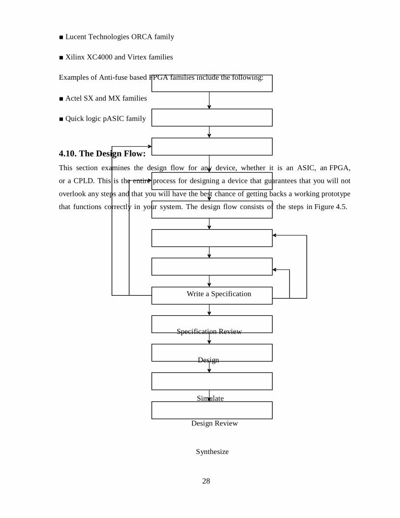
4.10. The Design Flow:
This section examines the design flow for any device, whether it is an ASIC, an FPGA,
or a CPLD. This is the entire process for designing a device that guarantees that you will not
overlook any steps and that you will have the best chance of getting backs a working prototype
that functions correctly in your system. The design flow consists of the steps in Figure 4.5.
Write a Specification
Specification Review
Design
Simulate
Design Review
Synthesize
Page 40
29
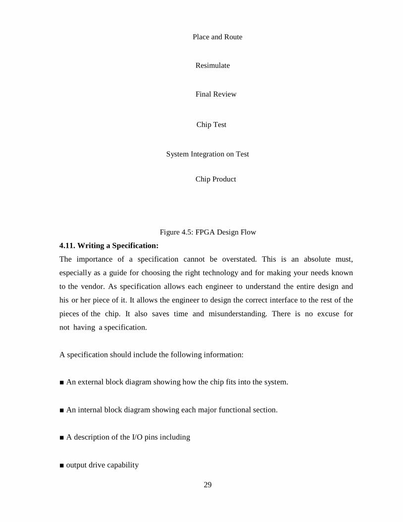
Place and Route
Resimulate
Final Review
Chip Test
System Integration on Test
Chip Product
Figure 4.5: FPGA Design Flow
4.11. Writing a Specification:
The importance of a specification cannot be overstated. This is an absolute must,
especially as a guide for choosing the right technology and for making your needs known
to the vendor. As specification allows each engineer to understand the entire design and
his or her piece of it. It allows the engineer to design the correct interface to the rest of the
pieces of the chip. It also saves time and misunderstanding. There is no excuse for
not having a specification.
A specification should include the following information:
■ An external block diagram showing how the chip fits into the system.
■ An internal block diagram showing each major functional section.
■ A description of the I/O pins including
■ output drive capability
Page 41
30
■ input threshold level
Timing estimates including
■ Setup and hold times for input pins
■ Propagation times for output pins
■ Clock cycle time
■ Estimated gate count
■ Package type
■ Target power consumption
■ Target price
■ Test procedures
It is also very important to understand that this is a living document. Many sections will have
best guesses in them, but these will change as the chip is being designed.
4.11.1 Choosing a Technology:
Once a specification has been written, it can be used to find the best vendor with a
technology and price structure that best meets your requirements.
4.11.2 Choosing a Design Entry Method:
You must decide at this point which design entry method you prefer. For smaller
chips, schematic entry is often the method of choice, especially if the design engineer
is already familiar with the tools. For larger designs, however, a hardware description
language (HDL) such as Verilog or VHDL is used because of its portability, flexibility,
Page 42
31
and readability. When using a high level language, synthesis software will be required to
―synthesize‖ the design. This means that the software creates low level gates from the high
level description.
4.11.3 Choosing a Synthesis Tool:
You must decide at this point which synthesis software you will be using if you plan to
design the FPGA with an HDL. This is important since each synthesis tool has
recommended or mandatory methods of designing hardware so that it can correctly perform
synthesis. It will be necessary to know these methods up front so that sections of the chip will
not need to be redesigned later on. At the end of this phase it is very important to have a
design review. All appropriate personnel should review the decisions to be certain that the
specification is correct, and that the correct technology and design entry method have been
chosen.
4.11.4 Designing the Chip:
It is very important to follow good design practices. This means taking into account the
following design issues that we discuss in detail later in this chapter.
■ Top-down design
■ Use logic that fits well with the architecture of the device you have chosen
■ Macros
■ Synchronous design
■ Protect against metastability
■ Avoid floating nodes
■ Avoid bus contention
4.11.5 Simulating - design review:
Simulation is an ongoing process while the design is being done. Small sections of the
Page 43
32
design should be simulated separately before hooking them up to larger sections.
There will be much iteration of design and simulation in order to get the correct
functionality. Once design and simulation are finished, another design review must take
place so that the design can be checked. It is important to get others to look over the
simulations and make sure that nothing was missed and that no improper assumption was
made. This is one of the most important reviews because it is only with correct and
complete simulation that you will know that your chip will work correctly in your system.
4.11.6 Synthesis:
If the design was entered using an HDL, the next step is to synthesize the chip. This
involves using synthesis software to optimally translate your register transfer level
(RTL) design into a gate level design that can be mapped to logic blocks in the FPGA.
This may involve specifying switches and optimization criteria in the HDL code, or
playing with parameters of the synthesis software in order to insure good timing and
utilization.
4.11.7 Place and Route:
The next step is to lay out the chip, resulting in a real physical design for a real chip. This
involves using the vendor‘s software tools to optimize the programming of the chip to
implement the design. Then the design is programmed into the chip.
4.11.8 Re-simulating - final review:
After layout, the chip must be re-simulated with the new timing numbers produced by the
actual layout. If everything has gone well up to this point, the new simulation results will
agree with the predicted results. Otherwise, there are three possible paths to go in the
design flow. If the problems encountered here are significant, sections of the FPGA may
need to be redesigned. If there are simply some marginal timing paths or the design is
slightly larger than the FPGA, it may be necessary to perform another synthesis with
better constraints or simply another place and route with better constraints. At this
point, a final review is necessary to confirm that nothing has been overlooked.
4.11.9 Testing:
Page 44
33
For a programmable device, you simply program the device and immediately have your
prototypes. You then have the responsibility to place these prototypes in your system
and determine that the entire system actually works correctly. If you have followed
the procedure up to this point, chances are very good that your system will perform
correctly with only minor problems. These problems can often be worked around by
modifying the system or changing the system software. These problems need to be tested
and documented so that they can be fixed on the next revision of the chip. System
integration and system testing is necessary at this point to insure that all parts of the
system work correctly together. When the chips are put into production, it is necessary to
have some sort of burn-in test of your system that continually tests your system over
some long amount of time. If a chip has been designed correctly, it will only fail
because of electrical or mechanical problems that will usually show up with this kind of
stress testing.
4.12 Design Issues:
In the next sections of this chapter, we will discuss those areas that are unique to FPGA
design or that are particularly critical to these devices.
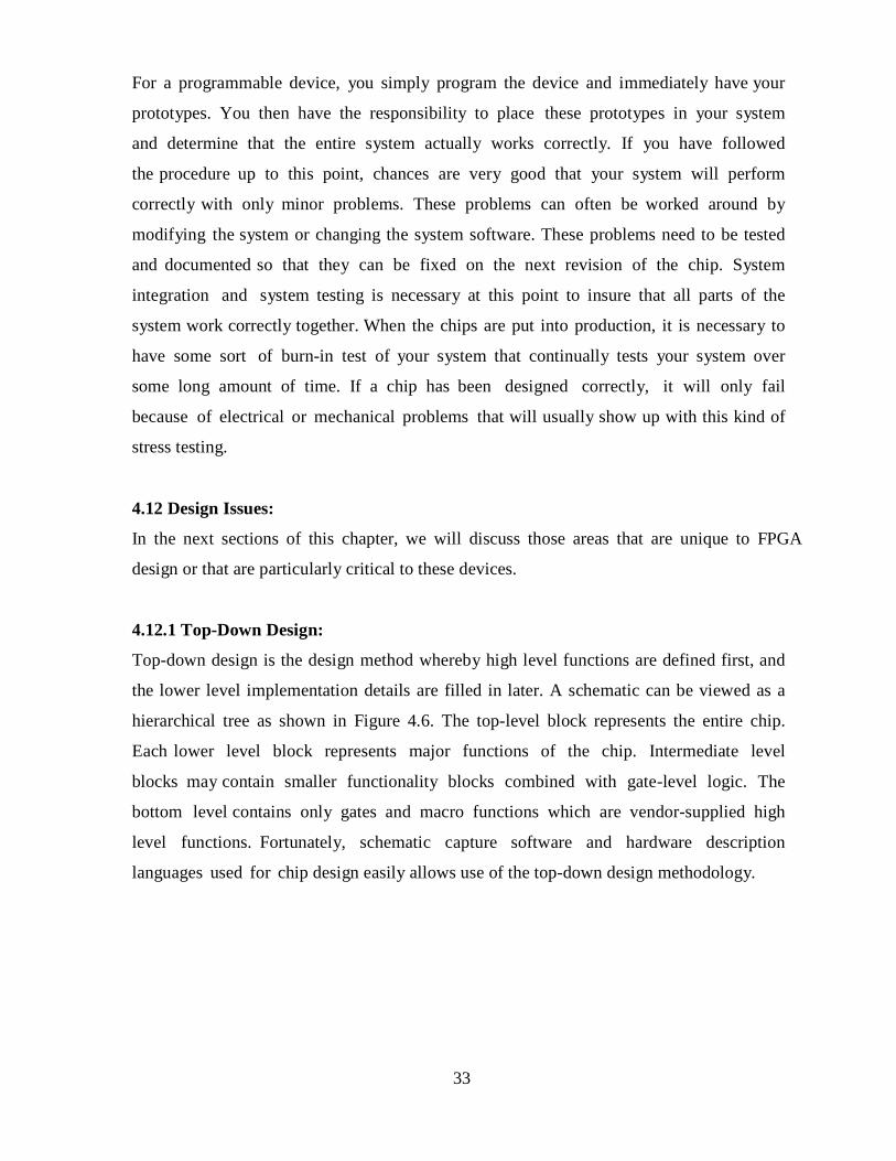
4.12.1 Top-Down Design:
Top-down design is the design method whereby high level functions are defined first, and
the lower level implementation details are filled in later. A schematic can be viewed as a
hierarchical tree as shown in Figure 4.6. The top-level block represents the entire chip.
Each lower level block represents major functions of the chip. Intermediate level
blocks may contain smaller functionality blocks combined with gate-level logic. The
bottom level contains only gates and macro functions which are vendor-supplied high
level functions. Fortunately, schematic capture software and hardware description
languages used for chip design easily allows use of the top-down design methodology.
Page 45
34
Figure 4.6: Top-Down Design
Top-down design is the preferred methodology for chip design for several reasons.
First, chips often incorporate a large number of gates and a very high level of
functionality. This methodology simplifies the design task and allows more than one
engineer, when necessary, to design the chip. Second, it allows flexibility in the design.
Sections can be removed and replaced with a higher-performance or optimized designs
without affecting other sections of the chip. Also important is the fact that simulation
is much simplified using this design methodology. Simulation is an extremely important
consideration in chip design since a chip cannot be blue-wired after production. For this
reason, simulation must be done extensively before the chip is sent for fabrication. A top-
down design approach allows each module to be simulated independently from the rest
of the design [25]. This is important for complex designs where an entire design can
take weeks to simulate and days to debug. Simulation is discussed in more detail later in
this chapter.
4.12.2 Keep the Architecture in Mind:
Look at the particular architecture to determine which logic devices fit best into it. The
vendor may be able to offer advice about this. Many synthesis packages can target their
results to a specific FPGA or CPLD family from a specific vendor, taking advantage of
Page 46
35
the architecture to provide you with faster, more optimal designs.
4.12.3 Synchronous Design:
One of the most important concepts in chip design, and one of the hardest to enforce
on novice chip designers, is that of synchronous design. Once a chip designer uncovers
a problem due to asynchronous design and attempts to fix it, he or she usually
becomes an evangelical convert to synchronous design. This is because asynchronous
design problems are due to marginal timing problems that may appear intermittently,
or may appear only when the vendor changes its semiconductor process. Asynchronous
designs that work for years in one process may suddenly fail when the chip is
manufactured using a newer process. Synchronous design simply means that all data is
passed through combinatorial logic and flip-flops that are synchronized to a single clock.
Delay is always controlled by flip-flops, not combinatorial logic. No signal that is
generated by combinatorial logic can be fed back to the same group of combinatorial
logic without first going through a synchronizing flip-flop. Clocks cannot be gated - in
other words, clocks must go directly to the clock inputs of the flip-flops without going
through any combinatorial logic. The following sections cover common asynchronous
design problems and how to fix them using synchronous logic.
4.13 Race conditions:
Figure 4.7 shows an asynchronous race condition where a clock signal is used to reset
a flip-flop. When SIG2 is low, the flip-flop is reset to a low state. On the rising edge of
SIG2, the designer wants the output to change to the high state of SIG1. Unfortunately,
since we don‘t know the exact internal timing of the flip-flop or the routing delay of the
signal to the clock versus the reset input, we cannot know which signal will arrive first -
the clock or the reset. This is a race condition. If the clock rising edge appears first, the
output will remain low. If the reset signal appears first, the output will go high. A slight
change in temperature, voltage, or process may cause a chip that works correctly to
suddenly work incorrectly. A more reliable synchronous solution is shown in Figure 4.8.
Here a faster clock is used, and the flip-flop is reset on the rising edge of the clock. This
circuit performs the same function, but as long as SIG1 and SIG2 are produced
synchronously - they change only after the rising edge of CLK - there is no race condition.
Page 47
36
Figure 4.7: Asynchronous: Race Condition
Figure 4.8: Synchronous: No Race Condition
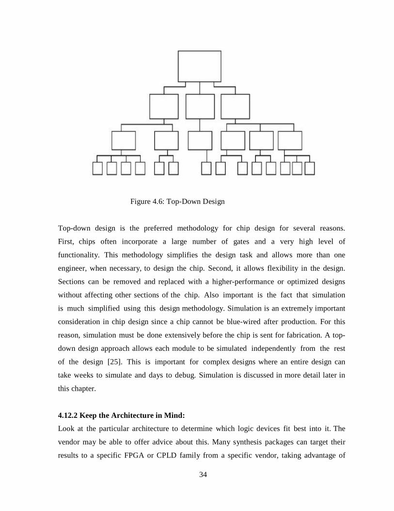
4.14 Delay dependent logic:
Figure 4.9 shows logic used to create a pulse. The pulse width depends very explicitly
on the delay of the individual logic gates. If the process should change, making the delay
shorter, the pulse width will shorten also, to the point where the logic that it feeds may not
recognize it at all. A synchronous pulse generator is shown in Figure 4.10. This pulse
depends only on the clock period. Changes to the process will not cause any significant
change in the pulse width.
Page 48
37
Figure 4.9: Asynchronous: Delay Dependent Logic
Figure 4.10: Synchronous: Delay Independent Logic
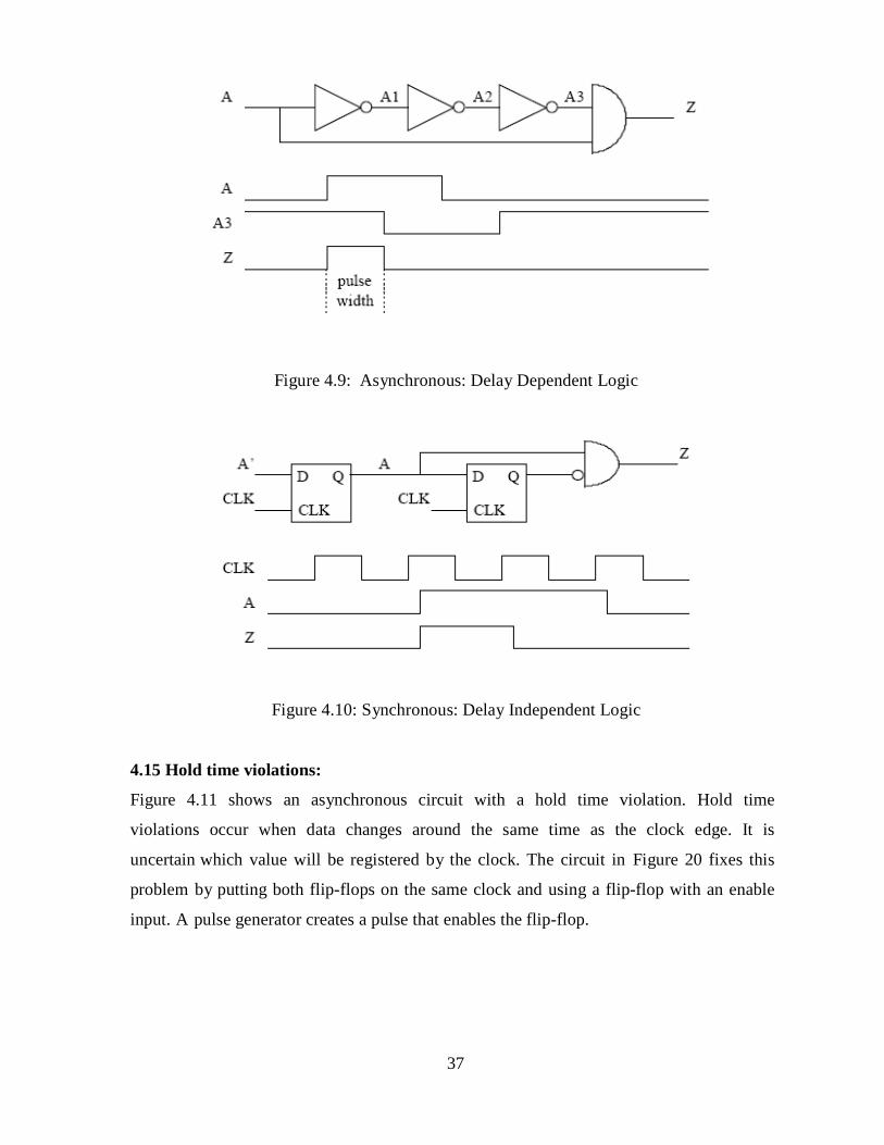
4.15 Hold time violations:
Figure 4.11 shows an asynchronous circuit with a hold time violation. Hold time
violations occur when data changes around the same time as the clock edge. It is
uncertain which value will be registered by the clock. The circuit in Figure 20 fixes this
problem by putting both flip-flops on the same clock and using a flip-flop with an enable
input. A pulse generator creates a pulse that enables the flip-flop.
Page 49
38
Figure 4.11: Asynchronous: Hold Time Violation
4.16 Glitches:
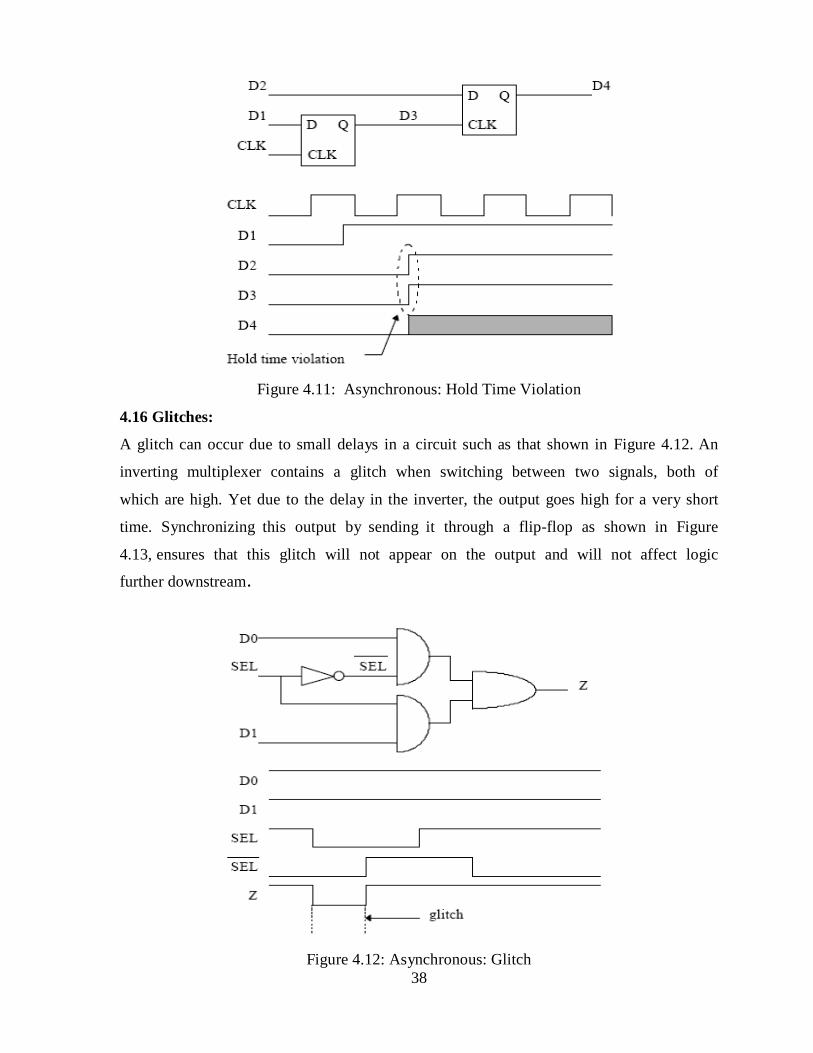
A glitch can occur due to small delays in a circuit such as that shown in Figure 4.12. An
inverting multiplexer contains a glitch when switching between two signals, both of
which are high. Yet due to the delay in the inverter, the output goes high for a very short
time. Synchronizing this output by sending it through a flip-flop as shown in Figure
4.13, ensures that this glitch will not appear on the output and will not affect logic
further downstream.
Figure 4.12: Asynchronous: Glitch
Page 50
39
Figure 4.13: Synchronous: No Glitch
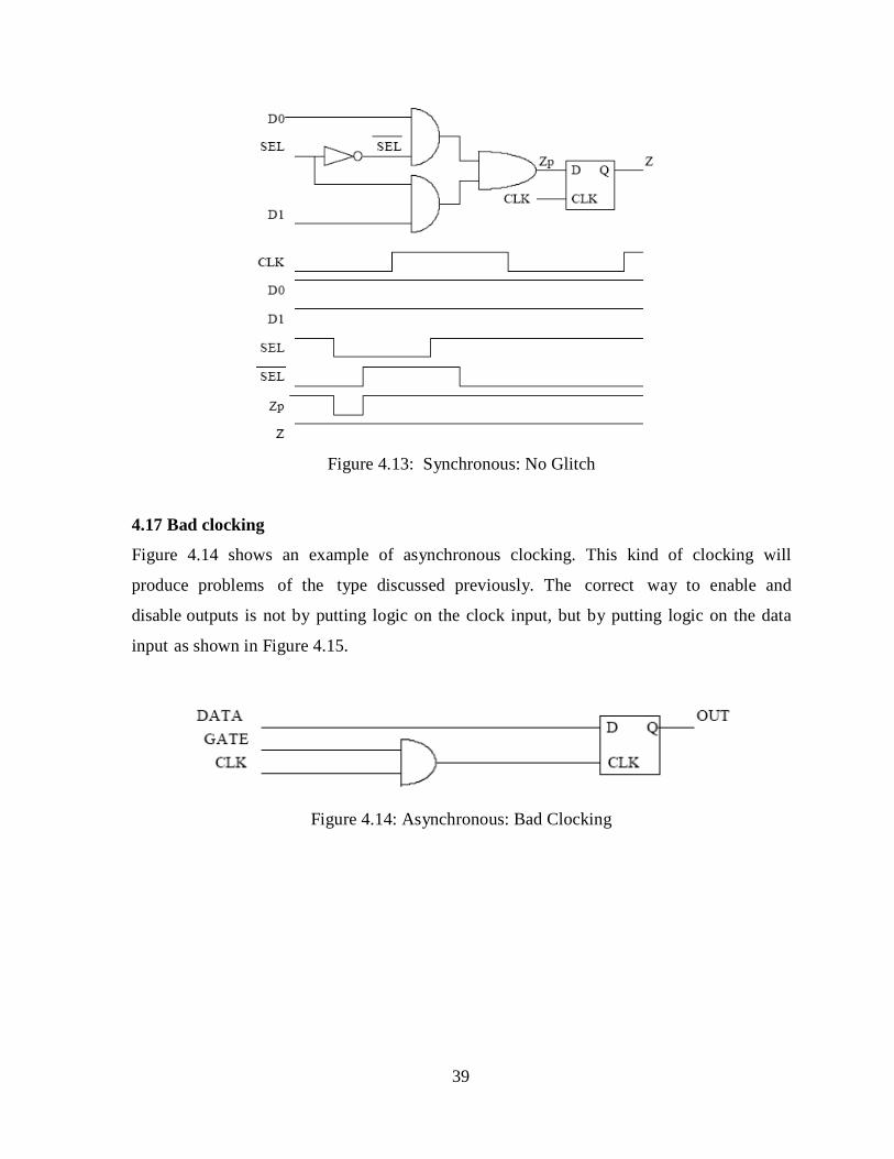
4.17 Bad clocking
Figure 4.14 shows an example of asynchronous clocking. This kind of clocking will
produce problems of the type discussed previously. The correct way to enable and
disable outputs is not by putting logic on the clock input, but by putting logic on the data
input as shown in Figure 4.15.
Figure 4.14: Asynchronous: Bad Clocking
Page 51
40
Figure 4.15: Synchronous: Good Clocking
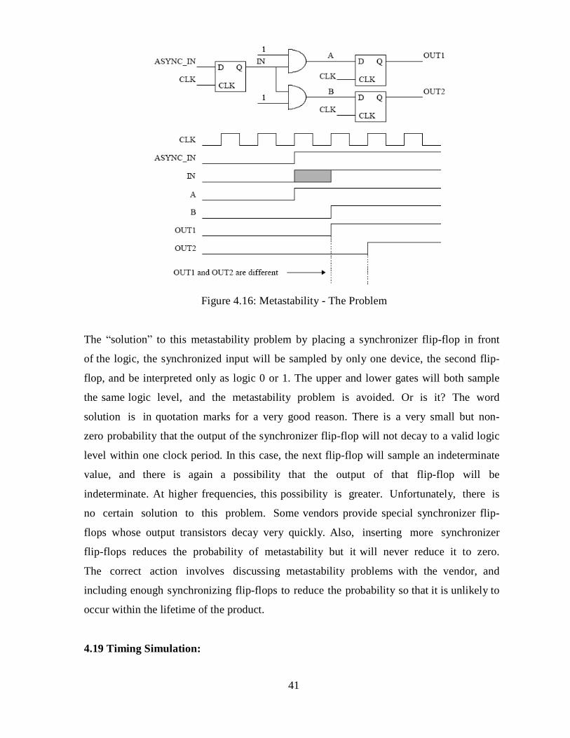
4.18 Metastability:
One of the great buzzwords, and often misunderstood concepts, of synchronous
design is metastability. Metastability refers to a condition which arises when
an asynchronous signal is clocked into a synchronous flip-flop. While chip designers
would prefer a completely synchronous world, the unfortunate fact is that signals coming
into a chip will depend on a user pushing a button or an interrupt from a processor, or will
be generated by a clock which is different from the one used by the chip. In these cases,
the asynchronous signal must be synchronized to the chip clock so that it can be used by
the internal circuitry. The designer must be careful how to do this in order to avoid
metastability problems as shown in Figure 4.16. If the ASYNC_IN signal goes high
around the same time as the clock, we have an unavoidable race condition [25]. The
output of the flip-flop can actually go to an undefined voltage level that is somewhere
between a logic 0 and logic 1. This is because an internal transistor did not have enough
time to fully charge to the correct level. This meta level may remain until the transistor
voltage leaks off or ―decays‖, or until the next clock cycle. During the clock cycle, the
gates that are connected to the output of the flip-flop may interpret this level differently.
In the figure, the upper gate sees the level as logic 1 whereas the lower gate sees it as
logic 0. In normal operation, OUT1 and OUT2 should always be the same value. In this
case, they are not and this could send the logic into an unexpected state from which it
may never return. This metastability can permanently lock up your chip.
Page 52
41
Figure 4.16: Metastability - The Problem
The ―solution‖ to this metastability problem by placing a synchronizer flip-flop in front
of the logic, the synchronized input will be sampled by only one device, the second flip-
flop, and be interpreted only as logic 0 or 1. The upper and lower gates will both sample
the same logic level, and the metastability problem is avoided. Or is it? The word
solution is in quotation marks for a very good reason. There is a very small but non-
zero probability that the output of the synchronizer flip-flop will not decay to a valid logic
level within one clock period. In this case, the next flip-flop will sample an indeterminate
value, and there is again a possibility that the output of that flip-flop will be
indeterminate. At higher frequencies, this possibility is greater. Unfortunately, there is
no certain solution to this problem. Some vendors provide special synchronizer flip-
flops whose output transistors decay very quickly. Also, inserting more synchronizer
flip-flops reduces the probability of metastability but it will never reduce it to zero.
The correct action involves discussing metastability problems with the vendor, and
including enough synchronizing flip-flops to reduce the probability so that it is unlikely to
occur within the lifetime of the product.
4.19 Timing Simulation:
Page 53
42
This method of timing analysis is growing less and less popular. It involves including
timing information in a functional simulation so that the real behavior of the chip
is simulated. The advantage of this kind of simulation is that timing and functional
problems can be examined and corrected. Also, asynchronous designs must use this type
of analysis because static timing analysis only works for synchronous designs. This is
another reason for designing synchronous chips only. As chips become larger, though,
this type of compute intensive simulation takes longer and longer to run. Also,
simulations can miss particular transitions that result in worst case results. This means that
certain long delay paths never get evaluated and a chip with timing problems can pass
timing simulation. If you do need to perform timing simulation, it is important to do
both worst case simulation and best case simulation. The term ―best case‖ can be
misleading. It refers to a chip that, due to voltage, temperature, and process variations, is
operating faster than the typical chip. However, hold time problems become apparent only
during the best case conditions
CHAPTER V
SYSTEM IMPLEMENTATION
Page 54
43
5.1 Introduction
This chapter covers the material on the implementation of Fast Fourier Transform and
Inverse Fast Fourier Transform design modules and verification of the design modules.
Behavioral synthesis is used to transfer the mathematical algorithm into VHDL program.
There are various types of architecture design for IFFT module. Some of the design use DSP
chip as the main part to implement the core-processing block, which is IFFT computation.
This issue has been discussed in the previous chapter and as stated in that chapter, FPGA is
the most cost effective to implement the design. As we know that, the IFFT transmitter
consists of several block or modules to implement the system using the IFFT function. After
consulting various books, white paper and journal, the proposed transmitter design is consist
of serial to parallel converter, modulator bank, processing block, parallel to serial converter
and cyclic prefix block module. This module block diagram is close to the standard for all
IFFT systems. It was in close accordance with the systems discussed in the primary resource
textbooks. These sources and several technical papers, served as useful tools to validate our
design.
5.2 Design Considerations
In general terms, the memory requirements for an N-point FFT are N locations for the real
data, N locations for the imaginary data, and N locations for the sinusoid data (sometimes
referred to as twiddle factors). Additional memory locations will be required if windowing is
used. Assuming the memory requirements are met, the DSP must perform the necessary
calculations in the required time. Many DSP vendors will either give a performance
benchmark for a specified FFT size or calculation time for a butterfly. When comparing FFT
specifications, it is important to make sure that the same type of FFT is used in all cases. For
example, the 1024-point FFT benchmark on one DSP derived from a radix-2 FFT should not
be compared with the radix-4 benchmark from another DSP.
Another consideration regarding FFTs is whether to use a fixed-point or a floating point
processor. The results of a butterfly calculation can be larger than the inputs to the butterfly.
This data growth can pose a potential problem in a DSP with a fixed number of bits. To
Page 55
44
prevent data overflow, the data needs to be scaled beforehand leaving enough extra bits for
growth. Alternatively, the data can be scaled after each stage of the FFT computation. The
technique of scaling data after each pass of the FFT is known as block floating point. It is
called this because a full array of data is scaled as a block regardless of whether or not each
element in the block needs to be scaled. The complete block is scaled so that the relative
relationship of each data word remains the same. For example, if each data word is shifted
right by one bit (divided by 2), the absolute values have been changed, but relative to each
other, the data stays the same.
The use of a floating-point DSP eliminates the need for data scaling and therefore results in a
simpler FFT routine, however the tradeoff is the increased processing time required for the
complex floating-point arithmetic.
The Real time FFT considerations may be summarized as
5.3 Implementation
When FFT and IFFT based FPGAs system design specify the architecture of FFT and
IFFT from a symbolic level, this level allows us using VHDL which stands for
VHSIC (Very High Speed Integrated Circuit) Hardware Programming Language VHDL
allows many levels of abstractions and permits accurate description of electronic
Page 56
45
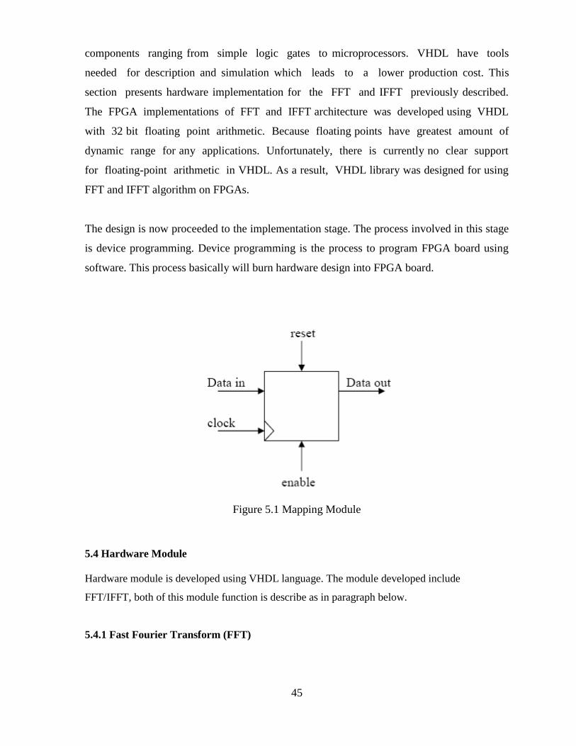
components ranging from simple logic gates to microprocessors. VHDL have tools
needed for description and simulation which leads to a lower production cost. This
section presents hardware implementation for the FFT and IFFT previously described.
The FPGA implementations of FFT and IFFT architecture was developed using VHDL
with 32 bit floating point arithmetic. Because floating points have greatest amount of
dynamic range for any applications. Unfortunately, there is currently no clear support
for floating-point arithmetic in VHDL. As a result, VHDL library was designed for using
FFT and IFFT algorithm on FPGAs.
The design is now proceeded to the implementation stage. The process involved in this stage
is device programming. Device programming is the process to program FPGA board using
software. This process basically will burn hardware design into FPGA board.
Figure 5.1 Mapping Module
5.4 Hardware Module
Hardware module is developed using VHDL language. The module developed include
FFT/IFFT, both of this module function is describe as in paragraph below.
5.4.1 Fast Fourier Transform (FFT)
Page 57
46
Figure 5.2 FFT module
Figure 5.2 show the block diagram for FFT module. This basic module consists of only two
inputs which is DataA and DataB. Opcode is used to select the operation performed by the
module. Result will be delivered through Result port. Several operations are performed by this
hardware where each operation executed in one clock cycle. Each operation is assigned to the
unique opcode value. Referring to the source code, FFT module has eight operations involved
such as addition, subtraction, multiplication, pass module and conversion from positive number
to negative.
5.4.2 Inverse Fast Fourier Transform (IFFT)
The same block diagram as FFT is used to develop IFFT module. Input port such as DataA,
DataB and Opcode is also used as well as Result for output port. The different between FFT and
IFFT is that the IFFT module needs to divide with eight at the end of the result. Additional
operation to handle this process is inserted at this module.
CHAPTER VI
DESIGN WALKTHROUGH
6.1 Introduction
This chapter discusses the methodology of the project and tools that involved in the process
to complete the design process of FFT/IFFT module in the FPGA hardware. The topic
basically covers on the usage of the VHDL software.
Page 58
47
The methodology of the project is basically divided into four main stages. These stages is
started with study the relevant topics and followed by the design process, implementation,
test and analysis stages. All stages are subdivided into several small topics or sub-stages and
explanation for each stage will be carried out in this chapter.
Each of the software function will be discussed in this chapter. For hardware part, a FPGA is
used and some documentation regarding this described in chapter 4.
6.2 Study Relevant Topics
Methodology of the project is divided into three main stages. The first stage will cover on
study the relevant topics. On this stage, the works is subdivided into three main topics which
is FFT and IFFT, VHDL programming and FPGA development board. These are the topics
that need to cover before moved into the design process. A study on FFT and IFFT is
required to understand the computation process. This requirement is important especially
during hardware development and software programming part. Bit representation in binary
also is another issue which require to study in this stage. Bit representation is crucial when
the multiplication or addition process involved point values such as twiddle factor. In VHDL
topic, there are two topic need to cover up which is Behavioral Modeling and Synthesis. The
last part in this stage is to study the FPGA development board.
6.3 Design Process
After all preparation in theoretical part is covered, the works is continued into the design
process stages. For this stage, the process is subdivided into several topics which are VHDL
design, VHDL analyzer, Logic Synthesis, device fitting, and design verification. These topics
actually are the process involved to complete the hardware design. Each of the process
required different software to accomplish the design.
VHDL design is the first steps to perform in the design process. The FFT/IFFT modules are
programmed in VHDL language. Basically this process is to generate the VHDL source
code. After generating the code, VHDL software is used to verify the generated code. The
Page 59
48
software will perform two processes which is VHDL analyzer and logic synthesis. VHDL
analyzer output is used as the logic synthesis and design verification. In logic synthesis, the
net list file which obtain from VHDL analyzer is synthesized base on the design constrain
and technology library available in the software. There are two types of simulation at the
design verification which is functional simulation and timing simulation. The functional
simulation is to simulate the hardware function and this process is not carried out since the
software used is not available. But the timing simulation is perform using Model Sim
software. The timing simulation is providing the timing function for the designed hardware.
The steps are listed below with brief description:
a. Design Entry. Enter the design into an ASIC design system, either by using hardware
description language (HDL) or schematic entry.
b. Logic Synthesis. Use an HDL (VHDL or Verilog) and a logic synthesis tool to produce a
netlist; netlist is a description of logic cells and their connections.
c. System Partitioning Divide the large system into ASIC-size pieces.
d. Prelayout Simulatio. Using stimulation tools such as Model Sim check whether the
designed system functions correctly.
e. Floor Planning Arrange the blocks of netlist on the chip.
f. Placement. Decide the location of cells in a block.
g. Routing Make the connections between cells and blocks.
h. Extraction. Determine the resistance and capacitance of the interconnections.
i. Post-Layout Stimulation Check whether the design works with the added loads.
Steps 1 through 4 are part of logical design, and steps 5 through 9 are part of physical design.
But there is some overlap; for example, system partitioning might be considered as either
logical or physical design. In other words, when performing system partitioning, designers
have to consider both logical and physical factors.
Page 61
50
6.4 Description of VHDL language
6.4.1 Very High Speed Integrated Circuits Hardware Descriptive Language
VHDL is an acronym, which stands for VHSIC hardware Description language VHSIC is yet
another acronym, which stands for very high, speed integrated circuits. VHDL can wear
many hats. It is being used for documentation, verification, and synthesis of large digital
design. This is actually one of the key features of VHDL, since the same VHDL code can
theoretically achieve all three of these goals, thus saving a lot of effort. In addition to being
used for each of these purposes, VHDL can be used to take three different approaches for
describing hardware. These three approaches are the structural, data flow and behavioral
methods of hardware description. Most of the times a mixture of the three methods are
employed. VHDL is a standard (VHDL- 1076) developed by IEEE (institute of electrical and
electronics engineers). VHDL is an industry standard language used to describe hardware
from the abstract to the concrete level. VHDL is rapidly being embraced as the universal
communication medium of design. Computer aided engineering workstation venders
throughout the industry are standardizing VHDL as input and output from their tools, etc.
Page 62
51
VHDL contains level of representations that can be used to representations all levels of
description from the bi-directional switch level in between. VHDL is designed to fulfill a
number of needs in the design process. First, it allows the description if the structure of the
design, that is how it can be decompose into sub-designs, and how these sub-designs are
interconnected. Secondly, it allows the specifications of the functions of the designs using
familiar programming language forms. Thirdly, as a result it allows a design to be simulated
before being manufactured so that designers can quickly compare alternatives and test for
correctness without the delay and the expense of hardware prototyping. VHDL is intended to
provide a tool that can be used by the digital systems community to distribute their designs in
a standard format using VHDL; they are able to talk to each other about their complex digital
circuit in a common language without the difficulties of revealing technical details. It is a
standard and unambiguous way of exchanging device and system models so that engineers
clear idea early in the design process where components from separate contractors may need
more work to function properly. It enables manufactures to document and archive electronics
systems and components in a common format allowing various parties to understand and
participate in the systems development.
As a standard description of digital systems, VHDL is used as input and output to various
simulations, synthesis and layout tools. The language provides the ability to describe
systems, networks and components at a very high behavioral level as well as very low gate
level. It also represents a top down methodology and environment. Simulation can be carried
out at any level from a generally functional analysis to a very detail gate level waveform
analysis. Synthesis is carried out currently only at the register level. A register transfer level
(RTL) description of hardware consists of a series of Boolean logic expression. Once a
VHDL design has been decomposed down to register level, a VHDL synthesizer can
generate the application specific integrate circuit (ASIC) representation or schematic for the
PC board layout.
Top-down design first describes the system at a very high level of abstraction, like a
specification. Designers simulate and debug the system at this very high level before refining
it into smaller components. The method describes each component at a high level and debugs
it alone and with other components in system. The design continues to be refined and debug
until it is complete down to its lowest building block. Mixed level design occurs when some
Page 63
52
components are a more detail level of description than others the advantage of the top down
design methodology is that engineers can discover and correct systems requirements and
timings. The tedious task of gate level design can be left to synthesis tools. The bottom line is
to reduce cost and faster time of manufacturing.
6.4.1.2 VHDL TERMINOLOGY
There are following VHDL terms in almost every description, along with some building
blocks that are defined in VHDL to mean something different to the average designer.
A. ENTITY
All designs are expressed in terms of entities. An entity is the most basic building block in a
design. The uppermost level of the design is the top-level entity. If the design is hierarchical
then the top-level description will have lower-level description contained in it. These lower-
level descriptions will be lower-level entity description.
The syntax for declaring an entity is:
entity_declaration ::=
entity identifier is
entity_header
entity_declarative_part
[ begin
entity_statement_part ]
end [ entity_simple_name ] ;
OR
Entity entity_name is
Port ( port_list);
end entity_name;
eg:
entity and_gate is
port (a: in std_logic;
b: in std_logic;
y: out std_logic);
end and_gate;
eg:
Page 64
53
entity deco8_3 is
port (a: in std_logic_vector(2 downto 0);
y: out std_logic_vector(7 downto 0));
end deco8_3;
MODES USED IN ENTITY
Signals in the port have a mode which indicates the driver direction. Modes also indicates
whether or not the port can be read from the entity 4 types of modes are used in VHDL
mode in
mode out
mode inout
Mode buffer
(i) mode in
Value can be read from it but can‘t be assigned to it.
Eg:
entity and_gate is
port (a: in std_logic;
b: in std_logic);
end and_gate;
(ii) mode out
Value can be assigned to it but can‘t be read from it.
Eg: entity and_gate is
port (y: out std_logic);
end and_gate;
(iii)mode inout
Value can be assigned can be read from it i.e. BIDIRECTIONAL.
Eg: entity and_gate is
port (x: inout std_logic);
end and_gate;
(iv) mode buffer
Output port with internal read capability.
Eg: entity and_gate is
port (w: buffer std_logic);
Page 65
54
end and_gate;
B. ARCHITECTURE
All entities that can be simulated have an architecture description. The architecture des-
cribes the behavior of the entity. A single entity can have multiple architecture. One
architecture might be behavioral another might be structural description of the design. An
architecture body is declared using the syntax:
architecture_body ::=
architecture identifier of entity_name is
architecture_declarative_part
begin
architecture_statement_part
end [ architecture_simple_name ] ;
architecture_declarative_part ::= { block_declarative_item }
architecture_statement_part ::= { concurrent_statement }
Architecture can contain only concurrent statements. A design can be described in an
architecture using levels of abstraction --
-- To facilitate faster design
-- Better understanding
-- Less complexity
The declarations in the architecture body define items that will be used to construct the
design description. In particular, signals and components may be declared here and used to
construct a structural description in terms of component instances.
C. CONFIGURATION
A configuration statement is used to bind component instants to an entity architecture pair. A
configuration can be considered like a part list for a design. It describes which behavior to use
for each entity much as a part list describes which part to use in the design.
D. GENERIC
A generic is VHDL term for a parameter that passes information to an entity for instance
if an entity is gate-level model with a rise and fall delay, the values for the rise and fall
Page 66
55
delays could be passed into the entity with generics.
E. PROCESS
A process is a basic unit of execution in VHDL. All operations that are performed in a
simulation of a VHDL description is broken into a single or multiple processes.
6.4.2. VHDL SUPERSEDING TRADITIONAL DESIGN METHODS
When a design engineer develops a new piece of hardware, today it is probably designed on
computer aides engineering (CAE) workstation. To create a design on a typical CAE
Workstation the designer will create a schematic for the design. A typical schematic consists
of symbols representing the basic units of the design connects together with signals The
symbols come from a library of parts that the designer uses to build the schematic. Those
symbols are wired together using signals (or nets, short for networks).The interconnection of
the symbols by signals creates the connections needed to specify the design. Such that the
net lists can be derived from the connections. A net list can be used to create. A simulation
model of the design to verify the design before it is built. Once the design has been verified,
the net list can be used to provide the information needed by a routing software package to
complete the actual design. The routing software will create the physical connection data to
create either the trace information needed for a PC board or the layer information needed for
an ASIC.
6.4.2.1 SYMBOL VS. ENTITY
Fig. 1.1 illustrates an example of a symbol used in a schematic. It is the symbol for a reset -
set flip-flop (RSFF). The symbol describes the following pieces of information to the
designer:
> The number of input pins for the device: In this example, the number is 2, set and reset.
> The number of output pins for the device: In this example, the number of output pins is 2 Q and QB
> The function of the device: In this example, the function of the device is described by the name of
the symbol. In the case, if simple gates the function of the symbol is described by the shape of the
symbol. Symbols specify the interface and the function to the designer.
Page 67
56
All designs are created from entities. An entity in VHDL corresponds directly to a symbol
in the traditional CAE workstation design methodology. Let us look at the top-level entity
for the rsff symbol described earlier. An entity for the RSff would look like this:
ENTITY rsff IS
PORT (set, reset: IN BIT;
Q, QB: BUFFER BIT);
END rsff;
The keyword ENTITY signifies that this is the start of an entity statement. In the
descriptions shown throughout the project , keywords of the language and types provided
with the STANDARD package will be shown in all CAPITAL letters. For instance, in the
example above the keywords are ENTITY, PORT ,IS BUFFER , etc. the standard type
provided in BIT. Names of user-created objects such as rsff, in the example above will be
shown in lower case italics. The name of the entity is rsff, as was the name of the symbol
described earlier. The entity has four ports in the PORT clause. Two ports are of mode IN
and two ports are of mode BUFFER. The reason for port mode BUFFER instead of just OUT
will be described later. The two input ports correspond directly to the two input pins on the
symbol from the workstation. The two buffer ports correspond directly to the two output
ports for the symbol. All of the ports have a type of BIT. The entity describes the interface
onto the outside world. It specifies the number of ports, the direction of the ports, and the
type of the ports. A lot more information can be put into the entity that is shown here, but
this will give us a foundation upon which we can later build.
6.4.2.2 SCHEMATIC VS. ARCHITECTURE
When the symbols are placed on a schematic sheet and wired together with signals, a
schematic for the design is formed. An example of a simple schematic for an RSFF is shown
in fig. The schematic contains two NAND gate symbol instances and four port instances.
Four nets connect the symbols and ports together to from the RS flip-flop. Each port has a
unique name, which also specifies the name of the signal connected to it. Each symbol
instance has a unique instance that identifies an instance for reference. When this schematic
is completed into a typical gate level simulator; it will function as an RSFF. A '0' level on the
reset port will cause the reset signal to have the value ‗0‘. This will cause the NAND gate U2
to output a '1' value on signal QB independent of the value on the other input of the NAND
gate. The '1' value on QB feeds back to one input of the NAND gate U1. If the set input is at
Page 68
57
an inactive value ('1'), then NAND gate U1 will have two '1' values as input, causing it to
output a value of '0' on the output Q . The RSF will have been reset. The schematic for the
RSff component also has a counterpart in VHDL, it is called architecture. Architecture is
always related to an entity and describes the behavior of that entity. Architecture for the rsff
device described above would look like this:
Fig. 6.1 R-S Flip-Flop
ARCHITECTURE net list of rsff IS
COMPONENT nand2
END COMPONEN;
BEGIN
U1: nand2
PORT MAP (set, Q, QB);
U2: nand2
PORT MAP (reset, Q QB);
END netlist ;
The keyword ARCHITECTURE signifies that this statement will describe architecture for
an Entity. The architecture name will be netlist. The entity that the architecture is describing
is called rsff . The reason for the connection between the architecture and the entity is that an
entity can have multiple architectures describing the behavior of the entity. For instance, one
architecture could be a behavioral description and another like the one shown above, could
be a structural description. The textual area between the keyword ARCHITECTURE and the
keyword BEGIN is where local signal and components are declared for later use. In this
example , there are two instances of a nand2 gate placed in the architecture. The compiler
needs to know what the interface to the component placed in the architecture are. The
component declaration statement will describe that information to the compiler . The
statement areas of the architecture start with the keyword BEGIN. All the statements
R
Clk
S
Q
Q’
Page 69
58
between the BEGIN and the END netlist statement are called concurrent statements, because
all of the statements execute concurrently.
6.4.3 VHDL DESIGN PROCESS
A design involves much more than meeting specifications. A good design must work
correctly in its environment even if the specifications do not specify it completely. Once The
design of schematic is done, the path from schematic to printed circuit board or silicon Is
fairly well automated by CAD tools. VHDL is a powerful tool to bridge the gap between
design specifications and the schematic generation. VHDL design terminology is aimed at
the following goals: -
Achieve first pass successes
Create a system level simulation of the design that operates together to verify the
Specifications
Create a single register-transfer level (RTL) model of each functional block that
can be used for logic simulation and as input for synthesis.
> Provide technology independent descriptions of the functional blocks.
> Provide a vendor independent description of the design .
> Each development of functional variation vectors for each functional block.
Create readable models as a means of documenting the design process for
customers as well for internal use.
The steps usually taken to verify a VHDL model for an existing device are :-
Pin definitions
Interfacing
Instruction set
Floating point
Test vectors
6.4.4 VHDL TEST - BENCH AND VERIFICATION
VHDL verification is performed using a set of modules and stimuli called VHDL test-bench.
The process of a test is to verify the functionality of a developed model or package. A test-
Bench should be a distinct design unit separated from the model or package to be verified,
placed in a design library separate from the model itself. The purpose of the verification is to
Page 70
59
verify that the developed model is correct, with few or no errors being found. It should not
be a means to locate errors in the VHDL code in order to patch them . If the test bench
incorporate models of components surrounding the model to be tested, they need only to
incorporate function‘s and interfaces required to properly operate with the model under test,
it is not necessary to develop complete VHDL models for them. If external stimuli or
configuration data is required, it should be implemented by reading an ASCII file in order to
ensure portability. Someone not involved in the creation of should perform the verification
that model or package, to avoid that a misunderstanding of the functionality is masked by the
same misunderstanding in the verification . A test-bench has three main purposes:
1. To generate stimulus for simulation ( waveform )
2. To apply this stimulus to the entity under test and collect the output responses
3. To compare output responses with expected values
A typical test-bench format is:
Entity TEST_BENCH is
End;
Architecture TB_BEHAVIOUR of TEST_BENCH is
Component ENTITY_UNDER_TEST
Port (list of ports, their types and modes );
End component;
Local signal declaration;
Begin
Generate-waveform-using behavioral-constructs;
Apply-2-entity-under-test;
EUT: ENTITY_UNDER_TEST port map (port - associations);
Monitor-values-and-compare-with-expected-values;
End TB_BEHAVIOUR;
Stimulus is automatically applied to the entity under test by instantiating the entity under
Test bench model and then specifying the appropriate signals .
6.4.5 VHDL MODELLING
VHDL modeling is performed in various details such as component model, board model and
system model. Every model is subject to verification. The main purpose of a .Model for
Page 71
60
component simulation is to be used for verification of a component under development,
before proceeding with the manufacture. This implies that the model should. Exactly reflect
the structures and functions of the underlying hardware, accurately being more important
than simulation speed. The model shall have correct timing characteristics, At least using
estimated (e.g. pre-layout) values for timing parameters.
The main purpose of a model for board-level simulation is to be used for verification of a
board using component , normally together with several other components . This can be
seen as the simulation version of bread boarding . This implies that the model must have
acceptable simulation speed , but only need to model the functionality possibly affecting the
board and other models . The model should be on the Register transfer level (RTL) or higher.
The model need necessarily not reflect the actual structure of the component.
The main purpose of the system level simulation is to provide the functionality of a board, a
subsystem, or a protocol, with a simulation speed allowing trade-offs to be performed. No
Similarity with any hardware is necessary, as long as the desired functionality is achieved.
The behavior may be approximated with respect to details such as tiling aspects, exactly
which clock cycle an event occurs, the exact numerical value of result, etc. VHDL modelings
Guidelines are rich and good references for VHDL modeling. It defines requirement on
VHDL models and test benches, and is intended to be used as an application document for
European Space Agency (ESA) development involving VHDL modeling. It is mainly
focused on digital models, specific requirements for analog modeling have not been covered.
6.4.5.1 STRUCTURAL STYLE OF MODELING
In the structural style of modeling, an entity is described as asset of interconnected
components. Such a model for HALF_ADDER entity is described in an architecture body as
shown below :
Architecture HA_STRUCTURE of HALF_ADDER is
Component XOR2
Port (X, Y: in BIT; Z: out BIT)
End Component;
Component AND
Port (L, M: in BIT; N: out BIT);
Page 72
61
End Component;
Begin
X1; XOR2 port map (A, B, SUM);
A1: AND2 port map (A, B, CARRY);
End HA_STRUCTURE;
The name of architecture body is HA_STRUCTURE. The entity declaration for HALF
_ADDER specifies the interface ports for this architecture body. The architecture body is
Composed of two parts: the declarative part (before the keyword begins) and the statement
parts (after the keywords begins). Two components declaration is present in the declarative
part of architecture body. These declarations specify the interface of components that are
used in the architecture body. The component XOR2 and AND2 May either is predefined
components in a library or, if they do not exist, they may late Bound to other components in
a library.
The declared components are instantiated in the statement part of the architecture body
using component instantiation statements X1 and A1 are components labels for these
components instantiation. The first component instantiation statement, labeled X1 shows
that signals A and B(the input ports of HALF_ADDER),are connected to the X and Y input
ports of XOR2 components, while output Z of this component is connected to output port
SUM of the HALF_ADDER entity. Similarly, in the second component instantiation
statement, signals A and B are connected to ports L and M of the AND2 component, while
port N is connected to the CARRY port of the HALF_ADDER. Note that in this case, the
signals in the port map of a component instantiation and the port signals in the component
declaration are associated by position (called positional association). The structural
representation for the HALF_ADDER does not say any thing about its functionality.
Separate entity models would be described for the components XOR2 and AND2, each
having its own entity declaration and architecture body.
A structural representation for the DECODER*4 entity:
Architecture DEC_STR of DECODER2*4 is
Component INV
Port (PIN: in BIT; POUT: out BIT);
Page 73
62
End component;
Component NAND3
Port (D0, D1, D2: in BIT; DZ: out BIT);
End component;
Signal ABAR, BBAR: Bit0;
Begin
V0: INV port map (A, ABAR);
V1: INV port map (B, BBAR);
N0: NAND3 port map (ENABLE, ABAR, BBAR, Z (0));
N1: NAND3 port map (ABAR, B, ENABLE, Z (1));
N2: NAND3 port map (A, BBAR, ENABLE, Z (2));
N3: NAND3 port map (A, B, ENABLE, Z (3));
End DEC_STR;
In this example, the name of the architecture body is DEC_STR, and it is associated with the
entity declaration with the name DECODER2*4; therefore, it inherits the list of interface
port from that entity declaration. In addition to the two component declarations
(for INV and NAND3), the architecture body contains a signal declaration that declares two
signals, ABAR and BBAR of type BIT. These signals, which represent wires, the used to
connect the various components that from the decoders. The scope of these signals is
restricted to the architecture body; therefore, these signals are not visible outside of
architecture body. Contrast these signals with the ports of an entity declaration, available for
use within any architecture body associated with the entity declaration. A component
instantiation statement is a concurrent statement. Therefore the order of the statements is not
important. The structural style of modeling describes only an interconnection of components
(viewed as black boxes 0, without implying any behavior of the components themselves nor
of the entity that they collectively represent. In the architecture body DEC_STR, the signal
A, B, and ENABLE used in the component instantiation statements are the input ports
declared in the DECODER2*4 entity declaration for example, in the components
instantiation labeled N3, port A is connected to input D0 of components NAND3, port B is
connected to the Input port D1 of components NAND3, port ENABLE is connected to the
output DZ and ports (3) of the DECODER2*4 entity is connected to the output port DZ of
component NAND3. Again, positional association is used to map signals in a port map of the
component instantiation with the ports of components specified in its declaration. The
Page 74
63
behavior of the component NAND3 and INV are not apparent, nor is the behavior of the
decoder entity that the structural model represents.
6.4.5.2 DATA FLOW OF MODELING
In this modeling style, the flow of the data through the entity is expressed primarily Using concurrent signal
assignment statements the structure of the entity is not explicitly Specified in this modeling style, but it can
be implicitly deduced. Consider the Following alternate architecture body for the HALF_ADDER entity that
uses this style.
Architecture HA_CONCURRENT of HALF_ADDER is
Begin
SUM<= A xor B after 8ns;
CARRY<= A and B after 4ns;
End HA_CONCURRENT;
The dataflow model for the HALF_ADDER is described using two concurrent signal
assignment statements (sequential signals assignment statements are described in the next
section). In a signal assignment statement, the symbol <= implies an assignment of a value
to a signal. The value of the expression on the right hand side of the statement is computed
and is assigned to the left hand side , called the target signal . A concurrent signal assignment
statement is executed only when any signal used in the expression on the right hand side has
an event on it , that is , for the signal change .
The architecture body consists of one signal declaration and six concurrent signals
assignment statements. The signal declaration declares signals ABAR and BBAR to be used
locally within the architecture body. In each of the signal assignments, no after clause was
used to specify delay. In all such cases, a default delay of 0 ns is assumed This Delay of 0 ns
is also known as delta and it represents as an infinitesimal delay. To the Behavior of this
architecture body, consider an event happening on one of the input signals, say, input port B
at time T. This would cause the concurrent signals assignment statement 1,3,and 6 to be
triggered. Their right- hand -side expression would be evaluated, and the corresponding
values would be scheduled to be assignee to the target signal at time (T+). When simulation
time advances to (T+), new values are assigned to signals Z (3) BBAR and Z (1). Since the
Page 75
64
value of BBAR changes, this will in turn trigger signal assignment statements 2 and 4.
Eventually, at time (t=20, signals Z (0) and Z (2) will be assigned their new values.
The semantics of this concurrent behavior indicate that the simulation as defined by the
language , is event triggered and that simulation time advance to the next time unit when an
event is scheduled to occur. Simulation time could also advance a multiple of delta time unit
. For example, events may have been scheduled to occur. At times 1,3, 4, 4+, 5, 6, 6+, 6+3,
10, 10+, 15, 15+ time units. The after clause may be used to generate a clock signal as shown
in the following concurrent signal assignment statement .
CLK<=not CLK after 10ns ... Signal CLK is of type BIT
This statement creates a periodic waveform on the signal CLK with a time period of
20ns as shown in figure below:
Figure 6.2 : A clock wave form with constant on–off period
6.4.5.3 BEHAVIORAL STYLE OF MODELING
In contrast to the styles of modeling described earlier, the behavioral style of modeling
specifies the behavior of an entity as a set of statements that are executed sequentially in the
specified order. This set of sequential statements, which are specified inside a process
statement, do not explicitly specify the structure of the entity but merely can appear within
an architecture body. For example consider the following behavior model for the DECODER
2*4 entity.
Architecture DEC_SEQUENTIAL of DECODER2*4 is
Begin
Process (A, B, ENABLE)
Variable ABAR, BBAR: BIT;
Begin
ABAR: = not A; ............. statement 1
Clk
10 20 30 40 50 60 70ns
Page 76
65
BBAR: = not B; ............. statement 2
If ENABLE = '1' then ............. statement 3
Z (3) <= not (A and B); ............. statement 4
Z (0) <= not (ABAR and BBAR); ............. statement 5
Z (2) <= not (A and BBAR); ............. statement 6
Z (1) <= not (ABAR and B); ............ statement 7
Else
Z<= "1111‖; ............. statement 8
End if;
End process;
End DEC_SEQUENTIAL;
A process statement also has a declarative part (before the keyword begin) and a statement
part (between the keywords begin and end process). The statements appearing within the
statement part are sequential statements and are executed sequel- -initially . The list of
signals specified within the parenthesis after the keyword process constitutes a sensitivity
list and the process statement is invoked whenever there is an event on any signal in this list.
In the previous example, when an event occurs on signal A, B or ENABLE, the statements
appearing within the process statement are executed sequentially. The variable declaration
(start with the keyword variable) declaration two variables called ABAR, BBAR. A variable
is different from a signal in that way it is always assigned a value instantaneously and the
assignment operator used is the := compound symbol; contrast this with a signal that is
assigned a value always after a certain delay (user specified or the default delta delay ), and
the assignment operator used to assign a value to a signal is the <= compound symbol.
Variable declared within a process have their scope limited to that process. Variables can
also be declared in subprograms; variable declared outside of a process or a process or a
subprogram are called shared variables. These variables can be updated and read by more
than one process. Note that signals cannot be declared within process. Signal assignment
statements appearing within a process are called sequential signal assignment statements.
Sequential signal assignment statements, including variable assignment statements are
executed sequentially independent of whether an event occurs on any signal in its right hand
side expression ; contrast this with the execution of concurrent signal assignment statements
in the data flow modeling style . In the previous architecture body, if any event occurs on
Page 77
66
any signal A, B, or ENABLE, statement 1, which is a variable assignment statement, is
executed then statement 2 is executed and so on, execution of the third statement, an if
statement, causes control to jump to the appropriate branch based on the value of the signal
ENABLE. If the value of ENABLE is ‗1‘, the next 4 signal assignment statements, 4 through
7 are executed independent of their respected values after delta delay. If ENABLE has a
value ‗0‘, a value of '1' is assigned is to each of the elements of the output array Z. When
execution reaches the end of the process, the process suspends itself and wait for another
event to occur on a signal in its sensitivity list. It is possible to use case or loop statements
within the process. The semantics and structure of these statements are very similar to those
in other high level programming like C or PASCAL.
An explicit wait statement can also be used to suspend a process. It can be used to wait for
certain amount of pan, until a certain condition becomes true, until an event occurs on one
or more signals here is an example of a process statement that generates a clock with a
different on a period .
Process
Begin
CLK <= '0';
Wait for 20ns;
CLK <='1';
Wait for 12ns;
End process;
This process does not have a sensitivity list because explicit wait statements are present
inside a process. It is important to remember that a process never terminates. It is always
either being executed or in a suspended state. All processes are executed once during the
initialization phase of simulation until they are suspended. Therefore, a process with no
sensitivity list and no explicit wait statement will never suspend itself. A signal can represent
not only a wire but also a placeholder for a value, that is , it can be used model a flip-flop.
Here is such an example; Port signal Q models a level-sensitive flip-flop.
Clk
0 10 32 52 64 84 96 ns
Page 78
67
Entity LS_DFF is
Port (Q: out BIT; D, CLK: in BIT) ;
End LS_DFF;
Architecture LS_DFF_BEH of LS_DFF is
Begin
Process (D, CLK)
Begin
If
CLK=1‘ then Q<=D;
End if;
End process;
End LS_DFF_BEH;
The process executes whenever there is an event on signal D or CLK. If the value of CLK is
‗1‘, the value of D is assigned to Q. if CLK is ‗0‘, then no assignment to Q takes place. Thus,
as long as CLK is ‗1‘, any change on D will appear on Q. once CLK becomes ‗0‘, the value
in Q is retained.
6.4.5.4 MIXED STYLE OF MODELING
It is possible to mix the three modeling styles that we have seen so far in signal architecture
body. That is, within an architecture body, That is, within an architecture body, we could use
component instantiation statement (that represent structure), concurrent signal assignment
statements (that represent dataflow), and process statements (that represent behavior). Here is
an example of a mixed style model for the one-bit figure below.
Entity FULL ADDER is
Port (A, B, CIN: in BIT; SUM, Cutout : out BIT);
End Full _ADDER;
architecture FA MIXED of FULL ADDER is
Component XOR2
Port (P1, P2: in BIT; PZ:out BIT);
end component; -
signal S1: BIT;
Begin
Page 79
68
Xl: XOR2 port map (A, B, S1);
Process (A, B, CIN)
Variable Ti, T2, 13: BIT);
Begin
T1: = A and B;
T1: = B and CIN:
T1: = A and CIN;
COUT <=T1 or T2 or T3;
End Process;
SUM <= S1 XOR Cin;
End DA_MIXED;
The full-adder is represented using one component instantiation statement, one process
statement, and one concurrent signal assignment statement. All of these statements are
concurrent statements; therefore, their order of appearance with the architecture: body is not
important. Note that a process statement itself is a concurrent statement; however, statement
within a process statement is always executed sequentially. S1 is a signal locally within the
architecture body and is used to pass the value from the output of the component Xl to the
expression for signal SUM.
6.4.5.5 STATE MACHINE MODELING
The machine can usually be modeled using a case statement in a process. The state
Information is stored in a signal. The multiple branches of the case statement contain the
behavior for each state.
The VHDL design modeling is self elucidated from the following Y-chart in general for any
circuit design.
Page 80
69
Figure 6.3 Y-chart
6.5 MATLAB
Page 81
70
Matlab is a multi purpose software which usually is used for mathematical computation in
the engineering field. In this project Matlab software is used for verification of FFT/IFFT
module.
Page 85
74
CHAPTER VIII
CONCLUSION AND CHALLENGES
8.1 Design Solution
As mentioned in the objectives, a FFT /IFFT module was successfully developed using FPGA
development board. The output from each module was tested using appropriate software to
ensure the correctness of the output result. Each of FFT/IFFT block was tested using Model Sim
and Matlab software during design process. This is to ensure that the hardware module was
correctly working when implemented in the FPGA hardware. During the implementation stage,
the operation for FFT/IFFT was tested using Matlab software. Since FFT/IFFT is based on
Page 86
75
mathematical operation, Matlab is the best platform to compare the computation result. The
comparison result shows that FFT/IFFT module is working correctly as the Matlab computation.
Some computation gives slightly different from Matlab especially in imaginary value and this
problem has been discussed in the implementation challenges section. Thus, based on the test
result, it was concluded that FFT/IFFT module is viable to be used in transmitter/receivers as
processing module.
The waveform result for these modules was given in result and simulation chapter and the
discussion regarding the operation of these modules was also made in above chapter. The design
can be further made to an improvement based on the suggestion discussed in later sections.
8.2 Suggestion for Future Research
Some recommendations are suggested to overcome the problem encountered during development
of this project. First is to use higher bit representation to represent the number. Instead of using 8
bit binary representation, use 16 bit or more to represent each number in binary. The reason of
using this method is to make the number representation can represent in more wide range of
number. Thus the risk of overflow problem will decrease. Beside that, selective code words also
can be used at the input such as input is limited from 0 to 64 for positive value of 8 bit binary
two‘s complement.
Use higher fixes point representation for point value representation. Floating point format also
can be considered as the solution to reduce error number representation especially for twiddle
factor value which is 0.7071. Although floating point consume processing time and output
latency, but it is an excellence method to overcome accuracy problem.
Beside that, it is suggested to create a circuit to detect the overflow by indicating the flag or
whatever way to ensure that the user know that the input given creates error to the system. The
user will notice this problem and will change the input value to ensure no error occurred.
In this design, the receiver module which is mainly using FFT is good at processing for the
positive input value. Therefore, any imaginary value should be mapped into real value such that
receiver can process the input data correctly.
For the future works, it is suggested to develop other modules such as interleaving, error
correction, QAM or QPSK modulation, cyclic prefix module and RF part. These modules will
make a complete set of system for transmitter and receiver.
Page 87
76
8.3 Implementation Challenges
This section covers on the analysis of the results obtained from the FFT and IFFT module.
The comparison results between Matlab and these modules were shown in the Table 7.1,
Table 7.2 and Table 7.3……………………………. in the previous chapter.
As notice from the comparison result, it can be concluded that the results obtained were not
exactly correct as using Matlab software for FFT/IFFT module. This section will present
some of the reason and discussed why this problem occurred and suggest the best solution for
the problem encountered.
8.3.1 Accuracy
The biggest problem when dealing with hardware in implementing mathematical computation is
the accuracy. The main reason why computation using hardware module is not accurate as using
software base is that the multiplication and division is using fix point number instead of floating
point. The weakness of using fix point representation is, approximation made for number
representation introduce error. For example decimal numbers for 0.7071 in binary is 010110101.
If this binary number converted back into decimal, the result is equal to 0.70. From this example,
it is proven that the twiddle factor is not represented accurately.
8.3.2 Multiplication of Twiddle Factor
Figure 8.1 Multiplication of Twiddle Multiplication
Figure 8.1 show an example of integer number multiply with twiddle factor in decimal and
binary representation. Result for decimal number can be shown up to 0.0001 point of
Page 88
77
accuracy. Compare to binary representation, the result obtained from computation only can
be displayed in 8 bit representation which is 7.The 8 bit number multiply with 8 bit number
will result 16 bit number. As we notice that, the result only can store 8 bit number thus, the
register only can store 7 instead of 7.7781 81 and consequently it sacrifice the accuracy. This
only involves one operation, since in FFT/IFFT requires many stages and many operations
the final result will be totally different at some of the output. In Matlab computation is done
all in floating point format and only during the final result, it is made rounded. Compared to
FPGA module, each operation is already having an error, thus obviously some output will not
given same value. Fix point number provide faster processing time, less circuit complexity
and less usage of memory module compared to floating point representation. The result
shown in this example is only for one multiplication. The result become worse if there are
more than two twiddle multiplication.
8.3.3 Division by eight in IFFT module
Figure 8.2 Example of twiddle multiplication
Figure 8.2 shows the example of division process at the IFFT module. In decimal, the result
can be shown accurately until up to 0.001. But for binary representation, the result can be
shown is 1. In binary, division process is represented as the multiplication process because it
simplifies the programming code. Division of 8 can be shown as multiplication of number
with 0.125.
Page 89
78
8.3.4 Overflow
Overflow is the main problem in binary representation for arithmetic process. Basically,
overflow is occurred when the value of carry in is not same as the value for carry out. Figure
8.3 depicts the example clearly.
Figure 8.3 Addition of decimal number
This example shows the addition of both positive decimal numbers. As mention before,
maximum positive number representation for 8 bit two‘s complement is 127. Thus in
decimal, additions of this number will results 252. But in binary two‘s complement, the value
252 is equal to -4. In this case, the result obtained for this addition will create an error result.
It can be concluded that the problem encountered are as discussed as above which leads to
the reason on why FPGA and Matlab computation gives different result. Some suggestion is
proposed and is stated at the last future section.
Page 90
79
References
[1] J. W. Cooley and J. W. Tukey, An Algorithm for the Machine Computation of
Complex Fourier Series, Mathematics Computation, Vol. 19, pp. 297-301, April 1965.
[2]A Family of Scalable FFT Architectures and an Implementation of 1024-Point Radix-
2 FFT for Real-Time Communications Adnan Suleiman1, Hani Saleh2, Adel Hussein3,
and David Akopian3 1Cirrus Logic, 2Intel Corporation, and 3 University of Texas at San
Antonio, Electrical and Computer Engineering Department
[3] A FAMILY OF MD FFT ALGORITHMS OF COMPLEXITY INTERMEDIATE
FFT BETWEEN THE MD COOLEY-TUKEY FFT AND THE MD PRIME-FACTOR R.
Bernardini, G. Cortelazzo, G.A. Mian Dipartimento di elettronica ed informatica
Universitzi di Padova Via Gradenigo 6A 35131 Padova, Italy
[4] A Partially Operated FFT/IFFT Processor for Low Complexity OFDM Modulation
and Demodulation of WiBro In-car Entertainment System ISCAS 2000 - IEEE
International Symposium on Circuits and Systems, May 28-31, 2000, Geneva,
Switzerland
[5] MINIMIZING THE MEMORY REQUIREMENT FOR CONTINUOUS FLOW FFT
IMPLEMENTATION: CONTINUOUS FLOW MIXED MODE FPT (CFMM-FFT) “R.
Radhouane, ‘P. Liu, *C. Modlin ―Laboratoire IEMN-DOAE, Universite de
Valenciennes, 593 13 Valenciennes Cedex 9. UMR CNRS 8520 ENSIMEV. FRANCE
[6] A Power-Scalable Reconfigurable FFT/IFFT IC Based on a Multi-Processor Ring
Guichang Zhong, Fan Xu, Member, IEEE, and Alan N. Willson, Jr., Fellow, IEEE
Page 91
80
[7] IEEE TRANSACTIONS ON CIRCUITS AND SYSTEMS—I: REGULAR PAPERS,
VOL. 54, NO. 4, APRIL 2007 807 Design of an FFT/IFFT Processor for MIMO OFDM
Systems Yu-Wei Lin and Chen-Yi Lee, Member, IEEE
[8] IEEE JOURNAL OF SOLID-STATE CIRCUITS, VOL. 40, NO. 8, AUGUST 2005
A 1-GS/s FFT/IFFT Processor for UWB Applications Yu-Wei Lin, Hsuan-Yu Liu, and
Chen-Yi Lee, Member, IEEE
[9] IMPLEMENTATION OF FFT AND IFFT ALGORITHMS IN FPGA : Ilgaz Az1
Suhap Sahin2 Cihan Karakuzu3 Mehmet Ali Çavuslu4 1,3,4 Departmant of Electronic
and Communication Engineering,Kocaeli University41040,_zmit,Kocaeli 2 Department
of Computer Engineering, Kocaeli University 41040,_zmit,Kocaeli
1e-mail : [email protected] 2e-mail : [email protected]
3e-mail : [email protected] 4e-mail : [email protected]
[10] A bit-serial FFT processor Eric Ericson Fabris; Gustavo André Hoffmann; Altamiro
Susin; Luigi Carro UFRGS Federal Univ. – Microelectronics Group Caixa Postal 15064
91501-970 Porto Alegre, Brazil {fabris, susin, carro}@inf.ufrgs.br {Gusthoff} @ieee.org
[11] A HIGH PERFORMANCE VLSI FFT ARCHITECTURE K. Babionitakis, K.
Manolopoulos, K. Nakos, D. Reisis, N. Vlassopoulos Electronics Laboratory, Department
of Physics National and Kapodistrian University of Athens Athens, Greece
[email protected] V.A. Chouliaras Department of Electronic and Electrical
Engineering, Loughborough University, Loughborough, LEICS, LE11 3TU, UK
[email protected]
[12] A Systolic FFT Architecture for Real Time FPGA Systems Preston A. Jackson, Cy
P. Chan, Jonathan E. Scalera, Charles M. Rader, and M. Michael Vai MIT Lincoln
Laboratory 244 Wood ST, Lexington, MA 02420
{preston,cychan,jscalera,cmr,mvai}@ll.mit.edu
[13] Steven W. Smith, The Scientist and Engineer‘s Guide to Digital Signal Processing,
Second Edition, 1999, California Technical Publishing, P.O. Box 502407, San Diego, CA
92150. Also available for free download at: http://www.dspguide.com or
http://www.analog.com
[14] A. V. Oppenheim and R. W. Schafer, Digital Signal Processing, Prentice- Hall,
1975.
[15] John G. Proakis and Dimitris G. Manolakis, Introduction to Digital Signal
Processing, MacMillian, 1988.
[16] ―Discrete-Time Signal Processing.‖ Alan V. Oppenheim, Ronald W. Schafer, PHI,
2001.
[17] ―Digital Signal Processing‖ Faruk Hussain, 2003.
Page 92
81
[18] ―Digital Signal Processing and Applications‖ Vallabhraj.