136
Dissertations in Forestry and Natural Sciences GAURAV BOSE DIFFRACTIVE OPTICS BASED ON V-SHAPED STRUCTURES AND ITS APPLICATIONS PUBLICATIONS OF THE UNIVERSITY OF EASTERN FINLAND

uef.fi
PUBLICATIONS OF THE UNIVERSITY OF EASTERN FINLAND
Dissertations in Forestry and Natural Sciences
ISBN 978-952-61-2330-1ISSN 1798-5668
Dissertations in Forestry and Natural Sciences
DIS
SE
RT
AT
ION
S | G
AU
RA
V B
OS
E | D
IFF
RA
CT
IVE
OP
TIC
S B
AS
ED
ON
V-S
HA
PE
D S
TR
UC
TU
RE
S A
ND
... | No
245
GAURAV BOSE
DIFFRACTIVE OPTICS BASED ON V-SHAPED STRUCTURES AND ITS APPLICATIONS
PUBLICATIONS OF THE UNIVERSITY OF EASTERN FINLAND
This book provides a survey of V-shaped diffractive structures and its applications.
Both exact and approximate methods are used to model the near-field interaction with the
wavelength scale scatterers. Several techniques to encode phase function in the form of modulating the structures are discussed
followed by the experimental demonstration of a triplicator. Further, the transition from
anti-to retro-reflection is demonstrated experimentally by testing several gratings with
different periods.
GAURAV BOSE


GAURAV BOSE
Diffractive optics based on
V-shaped structures
and its applications
Publications of the University of Eastern Finland
Dissertations in Forestry and Natural Sciences
No 245
Academic Dissertation
To be presented by permission of the Faculty of Science and Forestry for public
examination in the Auditorium E100 in Educa Building at the University of
Eastern Finland, Joensuu, on December, 13, 2016,
at 12 o’clock noon.
Institute of Photonics

Grano Oy
Jyvaskyla, 2016
Editors: Prof. Pertti Pasanen, Prof. Jukka Tuomela,
Prof. Pekka Toivanen, Prof. Matti Vornanen
Distribution:
University of Eastern Finland Library / Sales of publications
http://www.uef.fi/kirjasto
ISBN: 978-952-61-2330-1 (printed)
ISSNL: 1798-5668
ISSN: 1798-5668
ISBN: 978-952-61-2331-8 (pdf)
ISSNL: 1798-5668
ISSN: 1798-5676

Author’s address: University of Eastern Finland
Department of Physics and Mathematics
P.O. Box 111
80101 JOENSUU
FINLAND
email: [email protected]
Supervisors: Professor Jari Turunen, D.Sc.
University of Eastern Finland
Department of Physics and Mathematics
P.O. Box 111
80101 JOENSUU
FINLAND
email: [email protected]
Associate Professor Jani Tervo, Ph.D.
University of Eastern Finland
Department of Physics and Mathematics
P.O. Box 111
80101 JOENSUU
FINLAND
email:[email protected]
Professor Markku Kuittinen, Ph.D.
University of Eastern Finland
Department of Physics and Mathematics
P.O. Box 111
80101 JOENSUU
FINLAND
email: [email protected]
Reviewers: Nicolas Passilly, Ph.D.
Institut FEMTO-ST
Department of Micro Nano Sciences and Systems
15 B avenue des Montboucons
F-25030 Besancon Cedex
FRANCE
email: [email protected]
Fredrik Nikolajeff, Ph.D.
Uppsala University
Department of Engineering Sciences
P.O. Box 534
S-75121 UPPSALA
SWEDEN
email: [email protected]
Opponent: Professor Thierry Grosjean, Ph.D.
Institut FEMTO-ST
Departement dOptique P. M. Duffieux
15 B avenue des Montboucons
F-25030 Besancon Cedex
FRANCE
email: [email protected]

ABSTRACT
This thesis contains numerical and experimental studies on electro-
magnetic properties of micro- and nano-structured optical systems.
Since structures with features in the wavelength scale are consid-
ered, the Fourier Modal Method (FMM) is applied in the rigorous
numerical studies. The potentiality of diffractive elements with V-
shaped features is examined for several different applications.
A geometrical model based on the local plane interface approach
is introduced to study near-field effects, which involve interactions
of evanescent and inhomogeneous waves with a V-shaped dielec-
tric wedge, and the results are compared with rigorous FMM anal-
ysis. This geometrical model is shown to provide physical insight
in understanding the interaction of such waves, including surface
plasmons, with wavelength-scale scatterers.
Different coding schemes of high-carrier-frequency diffractive
optical elements are examined, which involve carrier gratings with
V-shaped features. In particular, a new method to realize reflective
position-modulated V-ridge diffractive elements is introduced. This
coding scheme is demonstrated by fabricating and characterizing a
triplicator for visible light.
We also study V-ridge gratings, whose facets are inclined at 45◦
compared to the surface normal and realize such gratings by using
precise mask alignment in the anisotropic wet etching process. Nu-
merical investigations are carried out to show the transition from
antireflection to retroreflection behavior of such gratings in the vis-
ible and the near-infrared wavelengths. The measurement results
show good agreement with theoretical results given by FMM.
Universal Decimal Classification: 535.42, 537.87, 681.7.02, 681.7.063
INSPEC Thesaurus: optics; micro-optics; diffractive optical elements; diffrac-
tion gratings; electromagnetic wave diffraction; light diffraction; light
propagation; optical fabrication; microfabrication; nanofabrication; metals;
electron beam lithography; etching; surface plasmons; Fourier analysis;
numerical analysis

Yleinen suomalainen asiasanasto: optiikka; optiset laitteet; mikrorakenteet;
nanorakenteet; metallit; valmistustekniikka; litografia; etsaus; numeerinen
analyysi


Preface
The thesis summarizes the work I did as a researcher in the In-
stitute of Photonics, Joensuu. Most of the findings were done by
sitting in front of the computer by reading journals, e-books and
running simulations. On several occasions I engrossed in physical
understanding and ended up staring at window leaving behind the
brewing sound of the coffee maker or the whirring of a CPU fan.
I would like to express my deepest gratitude to my supervi-
sors Prof. Jari Turunen, Dr. Jani Tervo for introducing me with the
field of diffractive optics. Without their effort this work would
not have been possible. I am also grateful to my third supervi-
sor Prof. Markku Kuittinen for his constant support and patience
with me. Their cumulative effort and guidance has made me where
I stand now and look further.
My sincere gratitude to Heikki, Ismo, Matthieu, Ton and Toni
for their wonderful cooperation at times whenever I needed them
in the form of simulation, fabrication or building setups. I extend
my gratitude to Pertti Paakkonen, Pertti Silfsten and Tommi Itko-
nen for providing me with the optical accessories for building my
setup. I would also like to thank Prof. Pasi Vahimaa and Prof. Timo
Jaaskelinen for providing me the opportunity to work in this de-
partment. I would like to acknowledge reviewers Dr. Nicolas Pas-
silly and Associate Prof. Fredrik Nikolajeff for their reviews and
comments. I am equally grateful to Prof. Thierry Grosjean who has
accepted to be my opponent in a very short notice.
The quietude was felt more without their presence, to name but
a few Rahul, Somnath, Juha, Henri, Noora, Kimmo, Leila, Bisrat
and Vishal. I would like to thank all of you for encouraging me
with all kinds of technical support. Rahul has been on my side in
every taxing situations.
In addition to all the foregoing, I would like to thank my wife
Samriddhi. Her unwavering love, support and motivation were

undeniably the basis on which the past 4 years of my life have been
built. Her tolerance of my invariably variable moods is a testament
in itself of her devotion and love. Extending my love to my elder
brother, without his support I could have never went abroad for
study. Finally my loveliest mother who hasn’t prioritized anything
before my education and happiness, to my adorable father who
couldn’t see me finishing this work but I believe he must be proud
of me once again.
Joensuu November 15, 2016 Gaurav Bose

Contents
1 INTRODUCTION 1
2 FUNDAMENTALS OF THE ELECTROMAGNETIC
THEORY OF LIGHT 7
2.1 Complex field representation . . . . . . . . . . . . . . 7
2.2 Macroscopic Maxwell’s equations . . . . . . . . . . . 9
2.3 Constitutive relations . . . . . . . . . . . . . . . . . . . 10
2.4 Boundary conditions . . . . . . . . . . . . . . . . . . . 13
2.5 Wave equations and the TE/TM decomposition . . . 13
2.6 Simplest solution of Maxwell’s equations . . . . . . . 15
3 INTERACTION OF LIGHT WITH MICRO-
STRUCTURED SURFACES 17
3.1 Reflection and transmission . . . . . . . . . . . . . . . 17
3.2 Angular spectrum representation . . . . . . . . . . . . 20
3.3 Scattering from periodic structures . . . . . . . . . . . 22
3.3.1 Eigenvalue problem in non-conical mounting 23
3.3.2 Boundary condition solution in multilayered
gratings . . . . . . . . . . . . . . . . . . . . . . 30
3.4 Effective medium theory . . . . . . . . . . . . . . . . . 32
3.5 Fundamentals of paraxial design methods . . . . . . 34
3.5.1 Thin element approximation . . . . . . . . . . 34
3.5.2 Local plane interface Approximation . . . . . 35
3.5.3 Iterative Fourier Transform Algorithm . . . . 36
4 LIGHT PROPAGATION IN WAVELENGTH
SCALE STRUCTURES 41
4.1 Near-field detection by the dielectric wedge . . . . . 41
4.1.1 Plane-wave incidence at high oblique angle . 42
4.1.2 Observation of evanescent-wave interference
patterns . . . . . . . . . . . . . . . . . . . . . . 47

4.2 Near field detection through a planar waveguide . . 49
4.2.1 Coupling efficiency from geometrical and rig-
orous models . . . . . . . . . . . . . . . . . . . 52
4.2.2 Detection of evanescent-wave interference pat-
terns . . . . . . . . . . . . . . . . . . . . . . . . 54
4.3 Metallic gratings with sub-wavelength slits . . . . . . 56
4.3.1 Geometrical configuration and models . . . . 56
4.3.2 Coupling efficiencies by rigorous theory and
the geometrical phase matching model . . . . 58
4.3.3 Examples of field patterns within the structure 61
4.3.4 Observation of surface plasmon interference . 63
4.4 Detection of evanescent fields above binary subwave-
length gratings . . . . . . . . . . . . . . . . . . . . . . 64
4.5 Summary . . . . . . . . . . . . . . . . . . . . . . . . . . 68
5 CODING OF HIGH-FREQUENCY CARRIER
V-SHAPE GRATINGS 71
5.1 V-groove width modulation . . . . . . . . . . . . . . . 73
5.1.1 Transmission-type groove width modulation . 74
5.1.2 Reflection-type groove width modulation . . . 75
5.2 V-ridge position modulation . . . . . . . . . . . . . . . 77
5.2.1 Reflection type ridge-position modulation . . 79
5.2.2 Coding of V-ridge structures . . . . . . . . . . 80
5.2.3 Numerical examples . . . . . . . . . . . . . . . 82
5.2.4 Effects of varying the wavelength and angle
of incidence . . . . . . . . . . . . . . . . . . . . 85
5.2.5 Transmission-type ridge position modulation 87
5.3 Fabrication . . . . . . . . . . . . . . . . . . . . . . . . . 89
5.4 Experimental results . . . . . . . . . . . . . . . . . . . 90
5.5 Summary . . . . . . . . . . . . . . . . . . . . . . . . . . 93
6 V-RIDGE GRATINGS: TRANSITION FROM
ANTIREFLECTION TO RETROREFLECTION 95
6.1 Geometry and principle . . . . . . . . . . . . . . . . . 96
6.2 Numerical simulations . . . . . . . . . . . . . . . . . . 96
6.2.1 Effect of varying the period . . . . . . . . . . . 97

6.2.2 Effect of varying the wavelength . . . . . . . . 98
6.2.3 Effect of finite substrate thickness . . . . . . . 100
6.2.4 Effect of varying flat bottom width . . . . . . 101
6.3 Experimental results . . . . . . . . . . . . . . . . . . . 102
6.4 Summary . . . . . . . . . . . . . . . . . . . . . . . . . . 105
7 CONCLUSIONS AND OUTLOOK 107
REFERENCES 109


1 Introduction
In elementary physics and optics textbooks, interference and diffrac-
tion phenomena are approached by fairly elementary concepts and
techniques based on the scalar theory of light [1]. In that context,
the Helmholtz equation is satisfied in free space propagation, and
diffraction by gratings is also treated by elementary approaches
based on scalar theory. However, if a field propagating in free space
is non-paraxial, one can no longer ignore the electromagnetic na-
ture of light since also the longitudinal components of the electric
and magnetic fields become significant. The same is true in grating
diffraction if the period of the grating is of the same order of mag-
nitude as the wavelength of light [2–5]. In this case the grating gen-
erates diffraction orders propagating in greatly differing directions
and, in addition, inhomogeneous waves that propagate along the
grating surface can become important. In this so-called resonance
domain a multitude of unexpected effects emerge, which can only
be predicted by rigorous diffraction theory, i.e., by determination of
the diffracted field by means of exact solution of Maxwell’s equa-
tions. This thesis contains studies of phenomena that occur in the
resonance domain. In particular, gratings and non-periodic struc-
tures involving V-shaped structural details are considered, along
with applications of such structures.
The basic concepts of the electromagnetic theory of light are dis-
cussed in chapter 2, where Maxwell’s equations, constitutive rela-
tions, and boundary conditions are introduced. In chapter 3 we first
discuss Fresnel’s equations that describe the reflection and trans-
mission of a plane wave incident at a plane boundary. We then pro-
ceed to discuss the exact solution of macroscopic Maxwell’s equa-
tions in the presence of more complicated geometric configurations,
namely diffraction gratings. There is a plethora of appropriate algo-
rithms for grating analysis, which are based on solving Maxwell’s
equations numerically at a price of vastly increased memory con-

Gaurav Bose: Diffractive optics based on V-shaped structures and itsapplications
sumption and computational time compared to simple scalar mod-
els [6–10]. Of these methods, we consider in particular the Fourier
modal method (FMM) [4], which is the one used throughout the
thesis whenever rigorous solutions are needed.
Apart from the high computational complexity, rigorous solu-
tions of grating diffraction problems do not always provide intu-
itive understanding of what happens inside the structure and why
resonant phenomena occur. Therefore, it is physically appealing to
supplement rigorous solutions of Maxwell’s equations by heuristic
descriptions of wave propagation inside the structure. When suc-
cessful, such descriptions could alleviate the numerical modeling
burden and, at the same time, retain the essence of the pertinent
physical phenomena and further exploit them in applications. It
is of substantial interest to see how far these heuristic elementary
approaches can be pushed in the modeling of diffraction by fine
structures, and to investigate how close to the rigorous results one
may get by exploiting them.
In an attempt to fill the gap between the approximate and ex-
act methods, Swanson [11] showed that the standard scalar the-
ory can be extended by ray tracing: he considered thick blazed
gratings by taking into account shadowing effects near the vertical
boundary of the triangular profile. These effects were studied fur-
ther in Refs. [12, 13], and multiple scattering effects were treated in
Refs. [14–16]. In another development [17], the regions of validity
of the scalar diffraction theory were investigated for binary gratings
by using the rigorous coupled wave technique [6]. In Refs. [18, 19],
a computationally efficient refinement of the thin-element approx-
imation for the analysis and design of binary gratings in the non-
paraxial domain was introduced.
In most of the heuristic studies mentioned above, the field in-
side wavelength-scale structures was modeled by geometrical rays
associated with sections of homogeneous plane waves. This type
of models are known as local plane-wave and local plane-interface
approximations. In chapter 4 of this thesis, we proceed one step
further in the local-plane-interface approach, by adding evanescent
2 Dissertations in Forestry and Natural Sciences No 245

Introduction
fields in the analysis. In particular, we describe tunneling of in-
homogeneous plane waves into V-shape structures and their prop-
agation though such structures. We gradually introduce different
geometries for generating evanescent, inhomogeneous, and plas-
mon waves to be detected by such V-shaped probes, comparing the
results with those of the Fourier modal method at all appropriate
instances.
The phase of a light wave can be influenced in several ways, in-
cluding retardation when the wave travels through a dielectric, by
phase jumps on reflection, and by the detour-phase principle [20].
In an elementary picture, the detour-phase principle can be best
understood by considering two rays leaving any two adjacent grat-
ing slits and propagating into the direction of the first order. In
the case of a regular grating there will always be a path difference
of one wavelength between these two rays, and hence the detour
phase equals 2π. If the grating slits are not in their perfect regular
positions, the detour phases between two adjacent rays varies as a
function of position and the diffracted wavefront will be deformed.
Lohmann used this idea to his advantage by realizing complex fil-
ter functions that lead to predefined far-field diffraction patterns,
which lead to the birth of computer-synthesized diffractive optics.
Apart from fixed diffractive elements, which can be fabricated accu-
rately by lithographic techniques, real-time reconfigurable elements
can be realized by means of spatial light modulators [21, 22]. To
mention just a few of the vast number of applications of synthetic
diffractive optics, elements based on the detour-phase principle can
be used in, e.g., optical data storage [23, 24], and in designing dis-
crete and continuous photonic bandgaps in the form of a shifted
Bragg grating in the single mode fiber [25].
In chapter 5 we introduce a new method to realize high-carrier-
frequency diffractive elements on the basis of the detour-phase prin-
ciple. We employ carrier gratings with V-shaped profiles as an al-
ternative to previously considered binary resonance-domain grat-
ings [26–28]. Several general techniques are discussed for the re-
alization of diffractive structures by modulation of the width and
Dissertations in Forestry and Natural Sciences No 245 3

Gaurav Bose: Diffractive optics based on V-shaped structures and itsapplications
position of the V-grooves or V-ridges in both reflection and trans-
mission modes of operation. Methods based on width modula-
tion are found to have severe limitations, whereas the approaches
based on position modulation prove highly successful. The pro-
posed position-modulation coding technique is demonstrated ex-
perimentally in the reflection mode by fabricating and character-
izing triplicators, which divide one incident plane wave into three
diffraction orders of equal efficiency.
In chapter 6, we examine V-ridge gratings whose half tip apex
angle is 45◦. We first investigate numerically the zeroth-order trans-
mittance and reflectance for different ratios d/λ of the grating pe-
riod d and the wavelength λ. With d/λ < 1, the gratings behave
as antireflection layers, and at d/λ ≫ 1 they gradually become
retroreflectors. The transition from antireflection to retroreflection
is demonstrated experimentally by fabricating and testing several
gratings with different periods, and good agreements with theoret-
ical results are observed.
Some of the aforementioned results have been published in the
following original articles and presented in the following interna-
tional and national conferences:
1 G. Bose, H. J. Hyvarinen, J. Tervo, and J. Turunen, “Geomet-
rical optics in the near field: local plane-interface approach
with evanescent waves,” Opt. Express 23, 330–339 (2015).
2 G. Bose, A. Verhoeven, I. Vartiainen, M. Roussey, M. Kuit-
tinen, J. Tervo, and J. Turunen “Diffractive optics based on
modulated subwavelength-domain V-ridge gratings,” J. Opt.
18, 085602 (2016).
3 G. Bose, H. J. Hyvarinen, J. Tervo, and J. Turunen, “Probing
Surface Plasmons by Bare V-shaped Tips: Modeling by Geo-
metrical Optics and Rigorous Diffraction Theory,” Opt. Rev.
(submitted).
4 G. Bose, H. J. Hyvarinen, J. Rahomaki, S. Rehman, J. Tervo,
and J. Turunen, “Near-field microscopy by surface-wave-assist-
4 Dissertations in Forestry and Natural Sciences No 245

Introduction
ed extraordinary transmission of light,” Optics Days (Helsinki,
Finland, poster presentation, 2013).
5 G. Bose, A. Verhoeven, M. Kuittinen, J. Tervo, and J. Turunen,
“V-groove high frequency carrier diffractive optical elements,”
Optics in Engineering (Joensuu, Finland, poster presentation,
2015).
6 G. Bose, H. J. Hyvarinen, J. Tervo, and J. Turunen, “Analysis of
surface plasmons by scanning near-field optical microscopes:
Modeling by geometrical optics and rigorous diffraction the-
ory,” Optics-photonics Design and Fabrication (Weingarten, Ger-
many, oral presentation, 2016).
Many of the results presented in chapters 4 and 5, and all results
presented in chapter 6 are still unpublished. Several original papers
related to these subjects are currently under preparation.
Dissertations in Forestry and Natural Sciences No 245 5

Gaurav Bose: Diffractive optics based on V-shaped structures and itsapplications
6 Dissertations in Forestry and Natural Sciences No 245

2 Fundamentals of the
electromagnetic theory
of light
The thesis deals with studies of electromagnetic properties of micro-
and nano-structured optical systems. Thereby it is important to un-
derstand the basic principles of the electromagnetic theory of light
and its propagation through any medium or in free space. This
chapter introduces the basic electromagnetic equations for that pur-
pose, which are used throughout the thesis.
2.1 COMPLEX FIELD REPRESENTATION
The measurable field quantities used in classical optics must be
real functions of position vector r and time t, which often leads
to complicated mathematics. Hence, it is mathematically more suit-
able to use the complex representation of electromagnetic fields. So
the convenient form of a monochromatic stationary time-harmonic
field of frequency ω0 can be expressed as
Ure(r, t) = ℜ{U(r) exp(−iω0t)} , (2.1)
where U(r) represents the complex amplitude of the real-valued
function Ure(r, t) that may be replaced with any of the vectors E(r),
H(r), D(r), B(r), and J(r), which are the electric field, the mag-
netic field, the electric displacement, the magnetic induction, and
the electric current density, respectively.
In order to describe polychromatic light, the time-harmonic rep-
resentation of the field in Eq. (2.1) must be generalized. To this end
we again define a unique complex counterpart of the real field.
Dissertations in Forestry and Natural Sciences No 245 7

Gaurav Bose: Diffractive optics based on V-shaped structures and itsapplications
Considering any real physical field quantity, we assume it to be
square integrable with respect to time, i.e,
∫ ∞
−∞U2
re(r, t)dt < ∞. (2.2)
Then we can represent Ure(r, t) as a temporal Fourier integral
Ure(r, t) =∫ ∞
−∞Ure(r, ω) exp(−iωt)dω, (2.3)
where
Ure(r, ω) =1
2π
∫ ∞
−∞Ure(r, t) exp(iωt)dt, (2.4)
and Ure(r, ω) is the spectral amplitude of the real field in the space-
frequency domain. The Fourier-transform pair of Eqs. (2.3) and
(2.4) shows us that any space-time domain vector field Ure(r, t)
may be expressed as a superposition of spectral complex ampli-
tudes Ure(r, ω) of time-harmonic fields.
Since the aforementioned space-time field is a real-valued func-
tion, the corresponding space-frequency complex function should
satisfy the complex conjugate relation
Ure(r,−ω) = U∗re(r, ω), (2.5)
where the asterisk ∗ denotes the complex conjugate. This relation
shows that the negative frequency components contains no new in-
formation that is not already contained in the positive components.
We may therefore introduce a new field representation by writing
U(r, ω) =
{
0 if ω < 0
2Ure(r, ω) if ω ≥ 0.(2.6)
The space-time domain counterpart of this quantity has a Fourier
representation
U(r, t) =∫ ∞
0U(r, ω) exp(−iωt)dω. (2.7)
8 Dissertations in Forestry and Natural Sciences No 245

CHAPTER 2. FUNDAMENTALS OF ELECTROMAGNETIC THEORY
The positive part of the spectrum in Eq. (2.6) only differs by a con-
stant factor of 2 from that of the original real function. This prop-
erty of the complex space-time domain function connects its Fourier
spectrum
U(r, ω) =1
2π
∫ ∞
−∞U(r, t) exp(iωt)dt (2.8)
to physically observable phenomena. Hence the quantity in Eq. (2.8)
represents the complex analytic signal [29]. In order to analyze any
scalar field quantity, like the electric charge density, a similar ap-
proach could be used.
2.2 MACROSCOPIC MAXWELL’S EQUATIONS
The fundamental laws of electrodynamics were introduced by J. C.
Maxwell [30] and hence they are called Maxwell’s equations. They
are a set of partial differential equations for calculating fields from
currents and charges. These equations have two variants, one of
which is the “microscopic” set of Maxwell’s equations that uses to-
tal charge and total current. On the other hand, the “macroscopic”
formulation is based on free charges and currents. In the context of
this thesis, the macroscopic set of Maxwell’s equations is of main
interest.
For complex-valued space-time domain fields, Maxwell’s equa-
tions may be presented as a set of four partial differential equations
∇× E(r, t) = − ∂
∂tB(r, t), (2.9)
∇× H(r, t) = J(r, t) +∂
∂tD(r, t), (2.10)
∇ · D(r, t) = ρ(r, t), (2.11)
∇ · B(r, t) = 0. (2.12)
The above equations are valid in any continuous media as well as in
vacuum. Now, considering Eq. (2.8), the above space-time domain
representation of Maxwell’s equations can be transformed into the
Dissertations in Forestry and Natural Sciences No 245 9

Gaurav Bose: Diffractive optics based on V-shaped structures and itsapplications
space frequency domain using the uniqueness of the Fourier trans-
form [31]. This leads to a set
∇× E(r, ω) = iωB(r, ω), (2.13)
∇× H(r, ω) = J(r)− iωD(r, ω), (2.14)
∇ · D(r, ω) = ρ(r, ω), (2.15)
∇ · B(r, ω) = 0, (2.16)
which is as general as the set of space-time domain Maxwell’s equa-
tions.
2.3 CONSTITUTIVE RELATIONS
In the macroscopic Maxwell’s equations, it is necessary to spec-
ify relationships between different space-time and space-frequency
field vectors introduced in the previous section, such as the elec-
tric displacement D and the electric field E, or the magnetic field
H and the magnetic induction B. These equations specify the re-
sponse of bound charges and currents to the applied fields, and
they are called constitutive relations. The relationship between the
electric field and the electric displacement may be expressed in the
form
D(r, t) = ǫ0E(r, t) + P(r, t), (2.17)
where ǫ0 is the electric permittivity in vacuum and the vector P is
known as the electric polarization. Analogously, by introducing the
magnetization vector M(r, t) and the magnetic permeability µ0 of
vacuum, we may write
H(r, t) =1
µ0B(r, t)− M(r, t) (2.18)
to specify the relationship between the magnetic field and the mag-
netic induction. Since magnetization is very small at optical fre-
quencies, the magnetic response of the material can be neglected
and a linear dependence of H on B can be assumed. From a causal-
ity argument [32], the relationship between polarization and the
10 Dissertations in Forestry and Natural Sciences No 245

CHAPTER 2. FUNDAMENTALS OF ELECTROMAGNETIC THEORY
electric field is linear and can be written as
P(r, t) =ǫ0
2π
∫ ∞
0χ(r, t′)E(r, t − t′)dt′, (2.19)
where χ(r, t) is the real-valued time-domain dielectric susceptibility
tensor. The dipole response of the material is independent of the
external electric field vector in any axes if the medium is isotropic.
The susceptibility tensor can then be written as
χ(r, t) = χ(r, t)I, (2.20)
where χ(r, t) is the scalar susceptibility and I is the identity matrix.
In analogy with Eq. (2.19), the relation between the internal elec-
tric current density and the electric field can be expressed as
J(r, t) =1
2π
∫ ∞
0σ(r, t′)E(r, t − t′), (2.21)
where the real-valued electric conductivity tensor σ(r, t) in space-
time domain reduces to scalar conductivity σ(r, t) in isotropic me-
dia. So, in view of Eqs. (2.17) and (2.19), the space-time dependent
electric displacement and electric field may be written as
D(r, t) =ǫ0
2π
∫ ∞
0ǫ(r, t′)E(r, t − t′)dt′. (2.22)
The space-time domain Maxwell’s equations together with con-
stitutive relations provide the required relations between different
field quantities. For mathematical convenience, however, the space-
frequency domain representation is typically preferable. Thereby,
with the help of the convolution theorem [33], the Fourier trans-
form of Eq. (2.19) can be expressed as
P(r, ω) = ǫ0χ(r, ω)E(r, ω), (2.23)
where the convolution in Eq. (2.19) is transformed into multiplica-
tion in the space-frequency domain. By applying the same proce-
dure to Eqs. (2.21) and (2.22) in non-magnetic media, we get a set
Dissertations in Forestry and Natural Sciences No 245 11

Gaurav Bose: Diffractive optics based on V-shaped structures and itsapplications
of three equations
D(r, ω) = ǫ0ǫ(r, ω)E(r, ω), (2.24)
B(r, ω) = µ0H(r, ω), (2.25)
J(r, ω) = σ(r, ω)E(r, ω), (2.26)
which connect the field vectors in Maxwell’s equations. These are
the constitutive or material equations in the space-frequency do-
main, and ǫ(r, ω) is known as the relative permittivity tensor. Sub-
stituting Eq. (2.17) and Eq. (2.23) in Eq. (2.24) and applying the
Fourier transform, we get
ǫ(r, ω) = 1 + χ(r, ω) = 1 +1
2π
∫ ∞
0χ(r, t) exp(iωt)dt, (2.27)
which is known as the dispersion law of the electric permittivity
tensor.
Let us now define a new quantity, known as the complex rela-
tive permittivity tensor, which connects the real relative permittiv-
ity and conductivity tensors as
ǫ(r, ω) = ǫ(r, ω) +i
ǫ0ωσ(r, ω). (2.28)
In isotropic media this tensor can again be replaced with a scalar
quantity ǫ(ω). In general, for optical frequencies and isotropic me-
dia, the complex refractive index is defined as
n(ω) = n(ω) + iκ(ω) =√
ǫ(ω) =√
ǫ′(ω) + iǫ′′(ω), (2.29)
where n(ω), κ(ω), ǫ′(ω), and ǫ′′(ω) are real functions. The attenu-
ation index κ determines the damping of the propagating wave in
the medium. Making use of the constitutive relations and Eq. (2.28),
we may write Eq. (2.14) as
∇× H(r, ω) = −iωǫ0 ǫ(r, ω)E(r, ω). (2.30)
In optics the charge density in Eq. (2.30) can in practice be written
equal to zero in Eq. (2.15). Using Eq. (2.24) we then get
∇ · [ǫ(r, ω)E(r, ω)] = 0. (2.31)
12 Dissertations in Forestry and Natural Sciences No 245

CHAPTER 2. FUNDAMENTALS OF ELECTROMAGNETIC THEORY
In conclusion, using the constitutive relations, we have obtained the
set
∇× E(r, ω) = iωB(r, ω), (2.32)
∇× H(r, ω) = −iωǫ0ǫ(r, ω)E(r, ω), (2.33)
∇ · [ǫ(r, ω)E(r, ω)] = 0, (2.34)
∇ · B(r, ω) = 0 (2.35)
of Maxwell’s equations in the space-frequency domain.
2.4 BOUNDARY CONDITIONS
Maxwell’s equations at any point r are valid if the medium in the
immediate vicinity of r is continuous, but quite often we encounter
abrupt boundaries between two different media. Therefore we need
relationships between the field components across such boundaries
of discontinuity. These boundary conditions can be derived from
the space-frequency Maxwell’s equations [34].
By defining a unit normal vector n12 pointing into the medium
with index 2 from a medium with index 1, we may write the elec-
tromagnetic boundary conditions in the form
n12 · (B2 − B1) = 0, (2.36)
n12 · (D2 − D1) = 0, (2.37)
n12 × (E2 − E1) = 0, (2.38)
n12 × (H2 − H1) = 0. (2.39)
These equations are valid across any discontinuity between dielec-
tric or conducting materials. They imply that the normal compo-
nents of B and D, as well as the tangential components of E and H,
are continuous across any boundary in a non-magnetic medium.
2.5 WAVE EQUATIONS AND THE TE/TM DECOMPOSITION
In order to derive wave equations and the so-called TE/TM de-
composition of Maxwell’s equations, we will make the following
assumptions:
Dissertations in Forestry and Natural Sciences No 245 13

Gaurav Bose: Diffractive optics based on V-shaped structures and itsapplications
1. A y-invariant system (the permittivity distribution and the
field are independent on the y-coordinate).
2. The incident field propagates in the xz-plane.
3. A homogeneous medium (constant refractive index).
4. An isotropic medium (no birefringence).
Since the medium is homogenous and isotropic, the complex per-
mittivity ǫ(ω) is independent on the spatial position and the direc-
tion of the diffracted wave. It now follows from Eqs. (2.32), (2.33),
and (2.25) that
∇× [∇× E(r, ω)] = ω2ǫ0µ0ǫ(ω)E(r, ω). (2.40)
By defining the speed of light c = (ǫ0µ0)−1/2 and using the vector
identity ∇ × (∇ × U) ≡ ∇(∇ · U) − ∇2U we get the Helmholtz
wave equation for the electric field:
∇2E(r, ω) + k20ǫ(ω)E(r, ω) = 0. (2.41)
Here the wave number k0 in vacuum is defined as k0 = 2π/λ =
ω/c, and λ is the vacuum wavelength of the field. Repeating similar
steps we get
∇2H(r, ω) + k20ǫ(ω)H(r, ω) = 0, (2.42)
which is the Helmholtz wave equation for the magnetic field.
Next, based on the above assumptions, we consider the geom-
etry in which all the partial derivatives in y-direction vanish in
Maxwell’s equations (y-invariant system). In this case Maxwell’s
equations can be divided in component form into two independent
sets:
Hx(x, z) =i
k0
√
ǫ0
µ0
∂
∂zEy(x, z), (2.43)
Hz(x, z) = − i
k0
√
ǫ0
µ0
∂
∂xEy(x, z), (2.44)
∂
∂zHx(x, z)− ∂
∂xHz(x, z) = −ik0(ǫ(x, z)
√
ǫ0
µ0Ey(x, z), (2.45)
14 Dissertations in Forestry and Natural Sciences No 245

CHAPTER 2. FUNDAMENTALS OF ELECTROMAGNETIC THEORY
and
Ex(x, z) = − i
k0 ǫ(x, z)
√
µ0
ǫ0
∂
∂zHy(x, z), (2.46)
Ez(x, z) =i
k0 ǫ(x, z)
√
µ0
ǫ0
∂
∂xHy(x, z), (2.47)
∂
∂zEy(x, z)− ∂
∂xEz(x, z) = ik0
√
µ0
ǫ0Hy(x, z). (2.48)
Clearly, Eqs. (2.43)–(2.45) contain only field components Ey, Hx and
Hz. Since the electric field is now perpendicular to the xz-plane,
this set of equations describes the transverse electric (TE) polariza-
tion of incident light. Similarly, Eqs. (2.46)–(2.48) contain only field
components Hy, Ex and Ez. Now the magnetic field is perpendic-
ular to the xz-plane, and one talks about transverse magnetic (TM)
polarization of incident light. By substituting Eqs. (2.43) and (2.44)
into (2.45), we obtain a single partial differential equation for the
y-component of the electric field in the form
∂2
∂x2Ey(x, z) +
∂2
∂z2Ey(x, z) + k2
0ǫ(x, z)Ey(x, z) = 0. (2.49)
Analogously, for TM polarization, we obtain an equation
∂
∂x
[
1
ǫ(x, z)
∂
∂xHy(x, z)
]
+∂
∂z
[
1
ǫ(x, z)
∂
∂zHy(x, z)
]
+ k20Hy(x, z) = 0,
(2.50)
which is mathematically slightly less attractive than Eq. (2.49).
2.6 SIMPLEST SOLUTION OF MAXWELL’S EQUATIONS
The electromagnetic plane wave is the simplest solution of Maxwell’s
equations. The space-frequency domain representation of an elec-
tromagnetic plane wave is as follows:
E(r, ω) = E0(ω) exp(ik · r), (2.51)
H(r, ω) = H0(ω) exp(ik · r), (2.52)
Dissertations in Forestry and Natural Sciences No 245 15

Gaurav Bose: Diffractive optics based on V-shaped structures and itsapplications
where the quantities E0(ω) and H0(ω) denote the vectorial complex
amplitudes of the electric and magnetic fields, respectively. The
wave vector k = kx x + kyy + kz z, where |k| = k0n, is perpendicular
to the planar wavefront and it defines the propagation direction of
the plane wave.
16 Dissertations in Forestry and Natural Sciences No 245

3 Interaction of light with
microstructured surfaces
There is no generally applicable and numerically efficient way to
describe the interaction of light with microstructured matter; the
most appropriate method depends, in particular, on the dimen-
sions of the features in the microstructure compared to the wave-
length of light. When these dimensions are comparable to the
wavelength, rigorous solutions of Maxwell’s equations are usually
required. If the dimensions are far larger than the wavelength, sim-
plified diffraction models can be applied, and even the use of geo-
metrical optics (Snell’s law and Fresnel’s equations) can sometimes
be justified. On the other hand, if the dimensions are much smaller
than the wavelength, effective refractive index approximations are
useful. In this chapter the mathematical methods needed in this
thesis for analyzing the interaction of light with corrugated inter-
faces are discussed.
3.1 REFLECTION AND TRANSMISSION
We begin by considering a plane wave with electric-field ampli-
tude Ei incident on a dielectric interface at an angle θi as shown in
Fig. 3.1. The interface separates two dielectric media. The refractive
index of the half-space z < 0 is denoted by ni and that of the half-
space z > 0 is denoted by nt. After the interaction with the interface
the incident field splits into a transmitted field denoted by Et and
a reflected field denoted by Er. The amplitudes and the intensi-
ties of the transmitted and reflected plane waves can be calculated
by taking into consideration the boundary conditions, which state
that certain components of the electromagnetic field are continuous
across the interface. The appropriate boundary conditions are dif-
Dissertations in Forestry and Natural Sciences No 245 17

Gaurav Bose: Diffractive optics based on V-shaped structures and itsapplications
ferent for the two polarization states of light, TE and TM. In the
case of TM polarization illustrated in Fig. 3.1(a), the magnetic field
vector is perpendicular to the plane of incidence, whereas in the
case of TE polarization the electric field vector is perpendicular to
this plane as shown in Fig. 3.1(b).
On applying the boundary conditions one first arrives at the law
of refraction
ni sin θi = nt sin θt, (3.1)
known as Snell’s law, and at the law of reflection θr = θi. Fur-
ther, by applying the boundary conditions, one can determine the
complex-amplitude transmission and reflection coefficients, known
as Fresnel coefficients, in the form
rTE =ETE
r
ETEi
=ni cos θi − nt cos θt
ni cos θi + nt cos θt, (3.2)
rTM =ETM
r
ETMi
=ni cos θt − nt cos θi
ni cos θt + nt cos θi, (3.3)
tTE =ETE
t
ETEi
=2ni cos θi
ni cos θi + nt cos θt, (3.4)
tTM =ETM
t
ETMi
=2ni cos θi
ni cos θt + nt cos θi. (3.5)
The reflection and transmission efficiencies, which characterize
the amount of reflected and transmitted energy, require some fur-
ther investigation. First, we recall that for real relative permittivity
ǫ = n2, the time-averaged Poynting vector P may be written as
P =ǫ0ck
2k0|E0|2 . (3.6)
The energy flow towards the surface under investigation and out-
wards from it is characterized by the z-component of the time-
averaged (spectral) Poynting vector, i.e.,
Pz =ǫ0ckz
2k0|E0|2 . (3.7)
18 Dissertations in Forestry and Natural Sciences No 245

CHAPTER 3. INTERACTION OF LIGHT WITH MICROSTRUCTURES
ki
kr
kt
ETMi
BTMi
ETMt
BTMt
ETMr
BTMr
x
z
ni nt
(a)
θr
θi
θt
x
z
ni nt
(b)
ki
kr
kt
ETEi
BTEi
ETEt
BTEt
ETEr
BTEr
θr
θi
θt
Figure 3.1: Direction of field and wave vectors in (a) TM polarization and (b) TE polar-
ization of the incident light.
Dissertations in Forestry and Natural Sciences No 245 19

Gaurav Bose: Diffractive optics based on V-shaped structures and itsapplications
By comparing the values of this quantity for the reflected and inci-
dent fields we obtain reflection efficiencies (reflectances)
RTE,TM = |rTE,TM|2. (3.8)
Correspondingly we obtain the transmission efficiencies (transmit-
tances)
TTE,TM =nt cos θt
ni cos θi|tTE,TM|2. (3.9)
The Fresnel equations can be extended to boundaries between di-
electric and absorbing materials simply by replacing nt with a com-
plex refractive index nt. The transmittance is therefore a meaningful
quantity only for real values of nt because the field decays rapidly
absorbing media. The reflectance is always a meaningful quantity,
since we assume that ni is real.
3.2 ANGULAR SPECTRUM REPRESENTATION
In the previous chapter we dealt with the fundamental Maxwell’s
equations and arrived at the plane-wave solution of the wave equa-
tion. The beauty of a plane wave is that it is the most fundamental
and mathematically simplest wave form to deal with. Any com-
plex electromagnetic field can be thought of as a superposition of
a finite or an infinite number of plane waves propagating in differ-
ent directions. Such an angular spectrum of plane waves is a basic,
physically appealing, and completely rigorous tool to study wave
propagation and diffraction homogeneous media in, e.g., the fields
of electrodynamics, optics, and acoustics. In the angular spectrum
representation different plane-wave components of the field have
variable amplitudes and propagation directions as we will see for-
mally below.
In the angular spectrum representation we choose an arbitrary
plane z = z0 = constant, in which the field E(x, y, z0) is assumed
to be known. The goal is to determine the field E(r) at any point
defined by a position vector r = (x, y, z) in space. To this end we
20 Dissertations in Forestry and Natural Sciences No 245

CHAPTER 3. INTERACTION OF LIGHT WITH MICROSTRUCTURES
first introduce the two-dimensional Fourier transform of the field E
at any plane z = constant:
E(kx, ky; z) =1
(2π)2
∫∫ ∞
−∞E(x, y, z) exp
[
−i(
kxx + kyy)]
dx dy,
(3.10)
where kx and ky are the spatial frequencies in the cartesian coordi-
nate system. The inverse of Eq. (3.10) reads as
E(x, y, z) =∫∫ ∞
−∞E(kx, ky; z) exp
[
i(
kxx + kyy)]
dkx dky. (3.11)
After inserting Eq. (3.10) into the Helmholtz equation (2.41) and
introducing the dispersion relation
kz =√
k2 − k2x − k2
y, (3.12)
where k = k0n, we find that the Fourier spectrum E evolves along
the z axis as
E(kx, ky; z) = E(kx, ky; z0) exp (±ikz∆z) , (3.13)
where ∆z = z − z0. Here the positive sign refers to forward propa-
gation towards the half-space z > z0 and the negative sign refers to
back-propagation into the half-space z < z0. We can conclude from
Eq. (3.13) that the angular spectrum at an arbitrary plane can be
obtained from the angular spectrum at z = z0 by multiplying with
the propagator exp (±ikzz) [35].
Inserting from Eq. (3.13) into Eq. (3.11), we finally arrive at the
angular spectrum representation
E(x, y, z) =∫∫ ∞
−∞E(kx, ky; z0) exp
[
i(
kxx + kyy ± kz∆z)]
dkx dky.
(3.14)
To propagate fields by the angular spectrum representation, we
therefore first evaluate E(kx, ky; z0) by Eq. (3.10), then use Eq. (3.13)
to propagate the angular spectrum, and finally return to the space
Dissertations in Forestry and Natural Sciences No 245 21
Gaurav Bose: Diffractive optics based on V-shaped structures and itsapplications
domain by means of Eq. (3.11). The direct and inverse Fourier trans-
forms involved in this process can be evaluated efficiently using the
Fast Fourier Transform algorithm.
In general, kz defined by Eq. (3.12) can have either real or imag-
inary values. If the only real-valued kz are non-zero, one speaks
about a free field. In general, however, the field contains also plane-
wave components with k2x + k2
y > k2, known as evanescent waves.
In this case kz becomes purely imaginary, i.e.,
kz = ±i√
k2x + k2
y − k2. (3.15)
Here the positive/negative sign is chosen when considering for-
ward/backward propagation. In either case, Eq. (3.15) implies an
exponential decay of the field in the propagation direction. Finally,
propagation in an absorbing medium can be governed simply by re-
placing k = k0n with a complex wave number k = k0n. In this case
all plane waves propagating in the medium are inhomogeneous and
the associated kz is a complex number.
3.3 SCATTERING FROM PERIODIC STRUCTURES
Analysis methods of microstructured optical elements such as grat-
ings are well established in the paraxial domain, where the elec-
tromagnetic properties of light can usually be ignored unless the
element modulates the state of polarization of the incident field in
a spatially varying fashion. However, in the non-paraxial domain,
the polarization of light and multiple scattering must be taken into
consideration in order to predict the interaction of light with the
microstructure correctly [2]. On the other hand, going beyond the
limitations of the scalar theory paves the way to a wide range of in-
teresting designs, which rely on exact solutions of both Maxwell’s
equations and electromagnetic boundary conditions. Several rigor-
ous methods exist for solving Maxwell’s equations, including dif-
ferential [36–38], integral [3, 39, 40], finite element [7, 8], and finite
difference [9, 10] techniques. However, the modal method to be
22 Dissertations in Forestry and Natural Sciences No 245

CHAPTER 3. INTERACTION OF LIGHT WITH MICROSTRUCTURES
described below is not only relatively easy to implement but also
trustworthy in most situations.
The Fourier Modal Method (FMM) is a widely used technique
to study the exact response of periodic scatterers (gratings) [4]. In
the homogeneous media on both sides of the modulated region the
rigorous solution of Maxwell’s equations is a Rayleigh expansion,
which is a discrete form of the angular spectrum representation. In-
side the grating the situation is more complicated, particularly if the
permittivity profile is z-dependent. In FMM we divide the modu-
lated region (slices) into layers, in each of which the refractive index
is invariant in the z-direction as illustrated in Fig. 3.2. The (gener-
ally complex) permittivity in each such slice is expressed as a trans-
verse Fourier series, and the fields inside the slices are expressed in
the form of pseudoperiodic (Floquet–Bloch) expansions [41]. These
expansions are transversely periodic apart from a common spatially
linear phase factor that depends on wave vector of the incident
plane wave. This leads to a solution of Maxwell’s equations in each
slice in terms of forward- and backward-propagating modal fields,
with z-dependence of the form exp(±iγz), where γ is the eigen-
value associated with the mode in question. Finally a set of bound-
ary value problems is solved numerically (by the so-called S-matrix
algorithm [42, 43]) to connect the solutions in each slice, and also
to the Rayleigh expansions outside the modulated region [44, 45].
The final result is a set complex amplitudes of the reflected and
transmitted diffraction orders. The method also allows the deter-
mination of field distributions inside the grating as superpositions
of the Bloch modes.
3.3.1 Eigenvalue problem in non-conical mounting
Let us next consider the FMM quantitatively under the following
assumptions (see Fig. 3.3):
1. The permittivity distribution ǫ is independent on the y coor-
dinate (linear grating).
Dissertations in Forestry and Natural Sciences No 245 23

Gaurav Bose: Diffractive optics based on V-shaped structures and itsapplications
replacements
x
z
slicing
w
d
α
I
II
III
Figure 3.2: Schematic representation of the way the cross section of the grating profile
is divided into z-invariant slices in FMM. Here a V-ridge grating with ridge width w,
half-angle α, and period d is considered as an example.
2. The incident plane wave arrives at non-conical mounting, i.e.,
it propagates in the xz-plane [46].
3. The permittivity distribution inside each layer z(j−1)< z <
z(j), j = 1, . . . , J, is independent on z.
4. The grating is periodic in the x-direction with period d.
In the case of a linear y-invariant grating, the complex permit-
tivity distribution inside the jth grating layer [2] is a function of x,
and it may be expressed in the form of a Fourier series
ǫ(j)(x) =∞
∑p=−∞
ǫ(j)p exp(i2πpx/d), (3.16)
where ǫ(j)p is the pth Fourier component of the complex permittivity,
given by
ǫ(j)p =
1
d
∫ d
0ǫ(j)(x) exp(−i2πpx/d)dx. (3.17)
In Sect. 2.5 we concluded that, in the case of a y-invariant grating,
Maxwell’s equations can be written in the component form for TE
and TM polarizations, respectively. For the TE polarization the only
24 Dissertations in Forestry and Natural Sciences No 245

CHAPTER 3. INTERACTION OF LIGHT WITH MICROSTRUCTURES
. . . . . .
z(0) z(1) z(j−1) z(j)z(J−1) z(J)
ǫ(J)(x)ǫ(j)(x)ǫ(1)(x)
ǫ(0) ǫ(J+1)
A(0,−)−1
Ai
A(0,−)0
A(0,−)1
A(J+1,+)−2
A(J+1,+)−1
A(J+1,+)0
A(J+1,+)1
x
z0
d
Figure 3.3: Basic geometry and notation used in the FMM for linear gratings.
non-vanishing electric field component is Ey. Hence the incident
field with amplitude Ai (see Fig. 3.3) can be expressed as
Ey,i(x, z) = Ai exp(
i{
kx,0x + kz,0
[
z − z(0)]})
, (3.18)
where
kz,0 =√
k20ǫ(0) − k2
x,0. (3.19)
Similarly, for the reflected field in homogenous space z < z(0), the
Rayleigh expansion may be written as
E(0,−)y (x, z) =
∞
∑m=−∞
A(0,−)m exp
(
i{
kx,mx + k(0)z,m
[
z − z(0)]})
, (3.20)
where kx,m = kx,0 + m2π/dx define the propagation direction of the
diffracted orders,
k(0)z,m =
√
k20ǫ(0) − k2
x,m, (3.21)
Dissertations in Forestry and Natural Sciences No 245 25

Gaurav Bose: Diffractive optics based on V-shaped structures and itsapplications
and A(0,−)m are the unknown amplitudes of the reflected diffraction
orders. Correspondingly, the field in the region z > z(J) has the
Rayleigh expansion
E(J+1,+)y (x, z) =
∞
∑m=−∞
A(J+1,+)m exp
(
i{
kx,mx + k(J)z,m
[
z − z(J)]})
,
(3.22)
where
k(J)z,m =
√
k20ǫ(J) − k2
x,m (3.23)
and A(J+1,+)m are the unknown amplitudes of the transmitted diffrac-
tion orders.
Since the electric field inside the grating is pseudoperiodic, it
may be expressed as a pseudo-Fourier series [47]
E(j)y (x, z) =
∞
∑m=−∞
U(j)y,m(z) exp(ikx,mx), (3.24)
where U(j)y,m(z) denotes the amplitude of the mth space-harmonic
field and is given by
U(j)y,m(z) =
1
d
∫ d
0E(j)y (x, z) exp(−ikx,mx)dx. (3.25)
Substituting the Fourier series expansion (3.16) of the complex per-
mittivity and the pseudo-Fourier series Eq. (3.24) into Eq. (2.49), we
get
−∞
∑m=−∞
k2x,mU
(j)y,m(z) exp(ikx,mx) +
∞
∑m=−∞
∂2
∂z2U
(j)y,m(z) exp(ikx,mx)
+ k20
∞
∑m=−∞
∞
∑p=−∞
ǫp exp(i2πpx/d)U(j)y,m(z) exp(ikx,mx) = 0.
(3.26)
Multiplying Eq. (3.26) by (1/d) exp(−ikx,qx), where q may be any
integer, and then integrating over the grating period from x = 0 to
x = d, we get
−k2x,qU
(j)q (z) +
∂2
∂z2U
(j)q (z) + k2
0
∞
∑m=−∞
ǫq−mU(j)y,m(z) = 0. (3.27)
26 Dissertations in Forestry and Natural Sciences No 245

CHAPTER 3. INTERACTION OF LIGHT WITH MICROSTRUCTURES
The general solution of Eq. (3.27) can now be written as
U(j)y,m(z) = U
(j)m exp
[
iγ(j)z]
, (3.28)
where γ(j) denotes the as-yet unknown eigenvalue of the mode.
Substituting Eq. (3.28) into Eq. (3.27) and rearranging terms, we
obtain
k20
∞
∑m=−∞
ǫq−mU(j)m − k2
x,qU(j)q = U
(j)q
[
γ(j)]2
. (3.29)
This equation has the form[
k20[[ǫ
(j)]]− kx
]
U(j) =[
Γ(j)]2
U(j) (3.30)
of a matrix eigenvalue problem for TE polarization, where the ele-
ments of the matrix kx are kx,q,m = k2x,qδq,m and δq,m denotes the Kro-
necker delta symbol [48]. We see at once that U(j) are the column
eigenvectors containing the Fourier components U(j)m,p, and the di-
agonal matrix [Γ(j)]2 contains the respective eigenvalues γ(j)p of the
matrix[
k20[[ǫ
(j)]]q−m − kx
]
. The eigenvectors and eigenvalues form
a discrete set such that the number of the eigenvectors and eigen-
values is same as one dimension of the matrix[
k20[[ǫ
(j)q−m]]− kx
]
.
It is of course not possible to solve numerically the eigenvalue
problem for a matrix with infinite dimensions, and therefore a trun-
cated set of eigenvectors and eigenvalues are computed up to a
finite index M, which also determines the number of diffraction or-
ders that are included in the analysis. By examining Eqs. (3.27) and
(2.38), we find that Ey is continuous over any discontinuities in the
x-direction. Therefore, the Fourier factorization product is of type
1 [49], i.e., Laurent’s rule can be applied to the truncated sum.
Once the matrix eigenvalue equation is solved, the general so-
lution for the field inside layer j can be written as
E(j)y,p(x, z) = exp
[
±iγ(j)p z
] M
∑m=−M
U(j)m,p exp(ikx,mx). (3.31)
The solution for[
Γ(j)]2
gives the propagation constants γ(j) in the
z-direction. The signs + and − denote the field modes propagating
Dissertations in Forestry and Natural Sciences No 245 27

Gaurav Bose: Diffractive optics based on V-shaped structures and itsapplications
in the positive and negative z-directions, respectively. To achieve
stability in the numerical solution it is important to choose the sign
of propagation constants properly. This is guaranteed if we choose
the sign according to the following rules:
1. If γ(j)p is complex, we choose its sign such that ℑ{γ(j)}p > 0.
2. If γ(j)p is real, we choose its sign such that ℜ{γ
(j)p } > 0.
Then, finally, we can write the general solution of the field inside
the layer region in the form
E(j)y (x, z) =
∞
∑p=1
(
a(j)p exp
{
iγ(j)p
[
z − z(j−1)]}
+ b(j)p exp
{
−iγ(j)p
[
z − z(j)]}) ∞
∑m=−∞
U(j)m,p exp (ikx,mx) ,
(3.32)
where a(j,±)p are yet undefined complex amplitudes of the forward
and backward propagating field components. These complex am-
plitudes are solved in the next section.
Finding the general solution for the field inside the modulated
in TM polarization is treated in a similar fashion. Now the only
non-vanishing magnetic field component is Hy, and therefore the
incident field is written as
Hy,i(x, z) = Ai exp(
i{
kx,0x + kz,0
[
z − z(0)]})
. (3.33)
The reflected and the transmitted TM Rayleigh fields in the homo-
geneous spaces may be represented in the form
H(0,−)y (x, z) =
M
∑m=−M
A(0,−)m exp
(
i{
kx,mx − k(0)z,m
[
z − z(0)]})
(3.34)
and
H(J+1,+)y (x, z) =
M
∑m=−M
A(J+1,+)m exp
(
i{
kx,mx + k0z,m
[
z − z(J+1)]})
.
(3.35)
28 Dissertations in Forestry and Natural Sciences No 245
CHAPTER 3. INTERACTION OF LIGHT WITH MICROSTRUCTURES
The x-and z-components of the electric field are now solved from
Eqs. (2.46) and (2.47).
Special attention is needed in solving the boundary conditions
for Hy and its derivatives across the discontinuities along the x-
direction by following the rules of Fourier factorization given by
Li [49]. We first obtain the basic differential equation
ǫ(j)(x)
{
k20H
(j)y (x, z) +
∂
∂x
[
1
ǫ(j)(x)
∂
∂xH
(j)y (x, z)
]}
= − ∂2
∂z2H
(j)y (x, z).
(3.36)
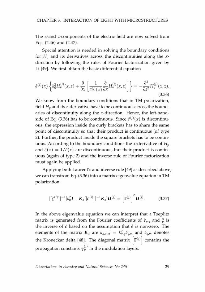
We know from the boundary conditions that in TM polarization,
field Hy and its z-derivative have to be continuous across the bound-
aries of discontinuity along the x-direction. Hence, the left-hand-
side of Eq. (3.36) has to be continuous. Since ǫ(j)(x) is discontinu-
ous, the expression inside the curly brackets has to share the same
point of discontinuity so that their product is continuous (of type
2). Further, the product inside the square brackets has to be contin-
uous. According to the boundary conditions the x-derivative of Hy
and ξ(x) = 1/ǫ(x) are discontinuous, but their product is contin-
uous (again of type 2) and the inverse rule of Fourier factorization
must again be applied.
Applying both Laurent’s and inverse rule [49] as described above,
we can transfrom Eq. (3.36) into a matrix eigenvalue equation in TM
polarization:
[[ξ(j) ]]−1[k20 I − Kx[[ǫ
(j)]]−1Kx]U(j) =
[
Γ(j)]2
U(j). (3.37)
In the above eigenvalue equation we can interpret that a Toeplitz
matrix is generated from the Fourier coefficients of ǫp,q and ξ is
the inverse of ǫ based on the assumption that ǫ is non-zero. The
elements of the matrix Kx are kx,q,m = k2x,qδq,m and δq,m denotes
the Kroneckar delta [48]. The diagonal matrix[
Γ(j)]
contains the
propagation constants γ(j)p in the modulation layers.
Dissertations in Forestry and Natural Sciences No 245 29

Gaurav Bose: Diffractive optics based on V-shaped structures and itsapplications
3.3.2 Boundary condition solution in multilayered gratings
In order to solve the boundary-value problem in multilayered grat-
ings illustrated in Fig. 3.3 we use S-matrix algorithm. A single S-
matrix of the multilayer structure represents the entire scattering
properties. In each layer the field is represented as superposition
of upward and downward propagating and decaying waves as de-
scribed by Eq. (3.32). We modify this equation slightly to simplify
the S-matrix derivation by introducing the notation
c(j)p = a
(j)p exp
[
iγ(j)p h(j)
]
, (3.38)
which represents the forward-propagating mode in the layer j, and
h(j) = z(j) − z(j−1). By satisfying the continuity of the tangential
field components across the interface of discontinuity, we may write
the boundary value problem in the matrix form[
U(j−1) U(j−1)
Q(j−1) −Q(j−1)
] [
c(j−1)
b(j−1)
]
=
[
U(j) U(j)
Q(j) −Q(j)
] [
χj−c(j)
χj+b(j)
]
, (3.39)
where Q(j) = U(j)Γ(j) and the diagonal matrices χ
(j)± contain the
elements exp[
±iγ(j)p h(j)δm,p
]
. The same boundary conditions also
hold at the boundaries z = z(0) and z = z(J) between the homoge-
neous regions and the sliced grating region. The vector c(0) con-
tains the complex input-field amplitudes in Eq. (3.18). In the case
of a plane wave of unit amplitude, c(0) = 1 and other elements of
the vector becomes zero. c(J+1) represents the complex amplitudes
of the transmitted fields and b(0) shows the complex amplitude of
the reflected fields.
Our goal is to find the S-matrix connecting output field with the
input field in the sense of a relation
[
c(j+1)
b(0)
]
= S(J+1)↔(0)
[
c(0)
b(j+1)
]
=
[
S(j+1)↔(0)11 S
(j+1)↔(0)12
S(j+1)↔(0)21 S
(j+1)↔(0)22
] [
c(0)
b(j+1)
]
, (3.40)
30 Dissertations in Forestry and Natural Sciences No 245

CHAPTER 3. INTERACTION OF LIGHT WITH MICROSTRUCTURES
where the notation (j + 1) ↔ (0) in the matrix S means that it
will be constructed from the plane J + 1 to the region 0 layer by
layer. Unfortunately, Eq. (3.40) can give rise to large numerical er-
rors in inverting the matrix S(j+1)↔(j)11 . For this reason we need to
reconsider Eq. (3.32) inside the jth grating layer and transform the
boundary value problem into the form
[
U(j) U(j)
Q(j) −Q(j)
] [
χ(j)+ a(j)
b(j)
]
=
[
U(j+1) U(j+1)
Q(j+1) −Q(j+1)
] [
a(j+1)
χ(j+1)+ b(j+1)
]
.
(3.41)
Now the S-matrix has been constructed starting from the region 0
and moving all the way to region J + 1 but this new matrix formula-
tion does not equal to S(J+1)↔(0) of the previous section. Therefore
a new matrix has been introduced as[
a(j)
b(0)
]
= W(0)↔(j)
[
a(0)
b(j)
]
=
[
W(0)↔(j)11 W
(0)↔(j)12
W(0)↔(j)21 W
(0)↔(j)22
] [
a(0)
b(j)
]
. (3.42)
Our goal is to find out W(0)↔(j+1) through the matrix W(0)↔(j). If
we again assume that there are no sources in the half-space z >
z(J), we can obtain the backward propagating field amplitudes from
Eqs. (3.38) and (3.40):
b(j) = S(J+1)↔(j)21 χ
(j)+ a(j). (3.43)
In view of Eqs. (3.41) and (3.42), we get the forward-propagating
field amplitudes from
a(j) =[
I − W(0)↔(j)12 S
(J+1)↔(j)21 χ
(j)+
]−1W
(0)↔(j)11 a(0). (3.44)
After some tedious calculations, we arrive at the matrix elements of
Eq. (3.42):
W(0)↔(j+1)11 = −
[
Y(0)↔(j+1)11 U(j) + Y
(0)↔(j+1)12 Q(j)
]
χ(j)+ W
(0)↔(j)11 ,
(3.45a)
W(0)↔(j+1)12 =
[
Y(0)↔(j+1)11 U(j+1) − Y
(0)↔(j+1)12 Q(j+1)
]
χ(j+1)+ , (3.45b)
Dissertations in Forestry and Natural Sciences No 245 31

Gaurav Bose: Diffractive optics based on V-shaped structures and itsapplications
where the matrix elements of Y(0) ↔ (j + 1) are defined as
Y(0)↔(j+1) =
[
Y(0)↔(j+1)11 Y
(0)↔(j+1)12
Y(0)↔(j+1)21 Y
(0)↔(j+1)22
]
=
[
−P(j+1) P(j)[χ(j)+ W
(0)↔(j)12 + I]
−Q(j+1) Q(j)[χ(j)+ W
(0)↔(j)12 − I]
]
. (3.46)
We can conclude from Eqs. (3.44) and (3.43) that S21 is the only ele-
ment in the whole S-matrix S(j+1)↔(j), and therefore we do not need
to solve the S-matrix element S(j+1)↔(j)11 . The complex amplitudes
of the transmitted field are finally obtained from Eq. (3.45a).
3.4 EFFECTIVE MEDIUM THEORY
When the grating period is significantly smaller than the wave-
length of incident light, d ≪ λ, only the zeroth reflected and trans-
mitted orders can propagate. In this case the modulated region
of the grating behaves as a homogenous effective medium hav-
ing a certain effective refractive index, and a simplified approach
known as the Effective Medium Theory (EMT) is available. The
treatment of the grating with the EMT approach makes the solu-
tion of the grating problem much faster because the transmittance
and the reflectance may be evaluated by thin film theory. This
type of permittivity-modulated media can show peculiar charac-
teristics such as form birefringence [50, 51]: light propagates with
different phase velocities depending on the state of polarization of
the incident field. This can be observed as a difference of refrac-
tive indices of different polarization modes, which further leads to
a polarization-dependent difference in the group velocity of light.
Furthermore, EMT provides clear physical insight into light propa-
gation in subwavelength-period gratings.
Let us consider the one-dimensional y-invariant grating illus-
trated in Fig. 3.4, where the triangular profile (other profiles could
be considered as well) is subdivided into J layers with equal thick-
ness h/J. Defining the fill factor in jth layer as f j = j/J, the dis-
tribution of refractive index within the modulated region may be
32 Dissertations in Forestry and Natural Sciences No 245

CHAPTER 3. INTERACTION OF LIGHT WITH MICROSTRUCTURES
n1
dw
h
x
z
n2α J layers
Figure 3.4: One-dimensional y-invariant linear grating: n1 and n2 denote the refractive
indices of the input region and the grating material, h is the height of the modulated
grating region, and w and d are the groove width and period of the grating, respectively.
written as
n(x) =
n1 when 0 6 x < f jd/2
n1 when d − f jd/2 6 x < d
n2 otherwise.
(3.47)
The effective refractive index in layer j is defined as the ratio of
the propagation constant γ(j) of a local Floquet–Bloch mode to the
free-space propagation constant k0,
n(j)eff =
γ(j)
k0. (3.48)
There can be more than one effective index depending on the num-
ber Floquet–Bloch modes that are excited in the grating, as we saw
above when dealing with FMM. However, in EMT we assume that
only the lowest-order TE and TM modes are significant and all oth-
ers can be ignored.
One way of deriving expressions for the effective refractive in-
dices is to retain only the zeroth modes in the FMM analysis. Con-
sidering Eq. (3.48) and the TM eigenvalue equation, we arrive at the
approximation for the effective refractive index [52]
njeff,⊥ =
[
f jn−21 +
(
1 − f j
)
n−22
]− 12 . (3.49)
Similarly, starting from the TE eigenvalue equation,
n(j)eff,‖ =
[
f jn21 +
(
1 − f j
)
n22
]
12 . (3.50)
Dissertations in Forestry and Natural Sciences No 245 33

Gaurav Bose: Diffractive optics based on V-shaped structures and itsapplications
Although the EMT is in principle applicable also to crossed (two-
dimensionally periodic) gratings, it is not possible to derive unique
expressions for the effective refractive indices from the FMM for-
mulation [53, 54].
3.5 FUNDAMENTALS OF PARAXIAL DESIGN METHODS
Exact analysis of diffraction gratings is computationally time con-
suming and challenging, especially for two-dimensional gratings
when the grating period is much larger than the wavelength. To
avoid such difficulties, approximate analysis methods such as the
Thin Element Approximations (TEA) [34] and Local Plane Interface
Approximation (LPIA) [11,55] can be applied under certain circum-
stances. In these methods, to be presented below, the response of
the modulated region is described by means of geometrical optics.
3.5.1 Thin element approximation
The thin element approximation method is one of the traditional
approximate analysis methods. It is usually applicable to gratings
whose minimum transverse feature size is in the order of ∼ 10λ and
the maximum grating thickness H is of the order of the wavelength.
With the above assumptions we assure that no significant energy
redistribution takes place in the transverse direction and field in
the modulated region can be treated locally as a plane wave. Then
optical path length calculations yield the field distribution just after
the element with sufficient accuracy.
Let us assume that the input field Ei propagates parallel to the
z-axis. If the modulated structure does not affect the state of polar-
ization of the incident field, we can write the transmitted field just
after the grating as
Et(x, H) = t(x)Ei(x, 0), (3.51)
where t(x) is known as the amplitude transmission function de-
34 Dissertations in Forestry and Natural Sciences No 245
CHAPTER 3. INTERACTION OF LIGHT WITH MICROSTRUCTURES
fined by
t(x) = exp
[
ik0
∫ H
0n(x, z)dz
]
(3.52)
(c.f. Fig. 3.5). If the modulated structure is a grating with period d,
the transmission function is periodic and may hence be expanded
in a Fourier series
t(x) =∞
∑m=−∞
Tm exp (i2πmx/d) , (3.53)
where
Tm =1
d
∫ d
0t(x) exp (−i2πmx/d) dx (3.54)
are the complex amplitudes of the transmitted diffraction orders.
Finally, the diffraction efficiencies of these orders are obtained from
ηm = |Tm|2 . (3.55)
The expressions given above can be readily extended to transversely
two-dimensionally modulated (periodic and non-periodic) struc-
tures.
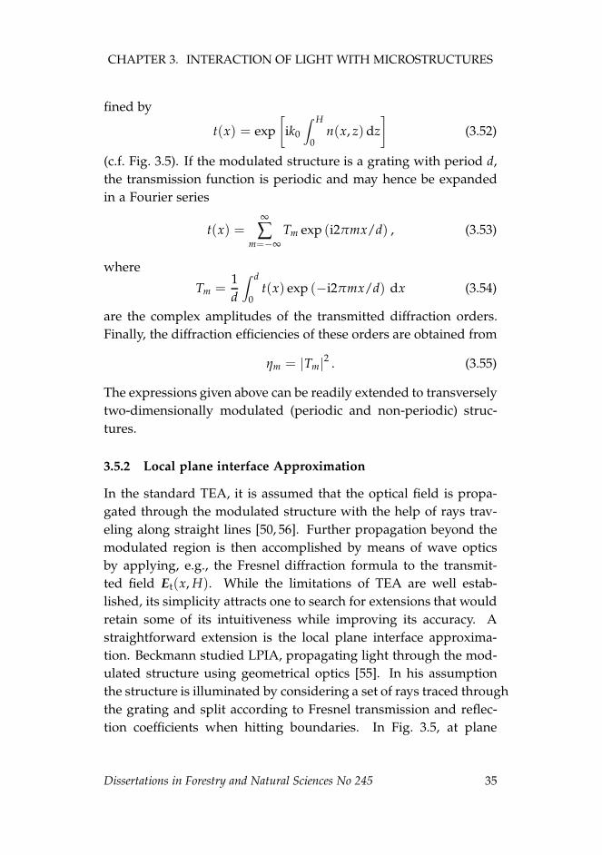
3.5.2 Local plane interface Approximation
In the standard TEA, it is assumed that the optical field is propa-
gated through the modulated structure with the help of rays trav-
eling along straight lines [50, 56]. Further propagation beyond the
modulated region is then accomplished by means of wave optics
by applying, e.g., the Fresnel diffraction formula to the transmit-
ted field Et(x, H). While the limitations of TEA are well estab-
lished, its simplicity attracts one to search for extensions that would
retain some of its intuitiveness while improving its accuracy. A
straightforward extension is the local plane interface approxima-
tion. Beckmann studied LPIA, propagating light through the mod-
ulated structure using geometrical optics [55]. In his assumption
the structure is illuminated by considering a set of rays traced through
the grating and split according to Fresnel transmission and reflec-
tion coefficients when hitting boundaries. In Fig. 3.5, at plane
Dissertations in Forestry and Natural Sciences No 245 35

Gaurav Bose: Diffractive optics based on V-shaped structures and itsapplications
.
.
.
.
.
.
.
.
.
.
.
.
0 Hz
h(x)
x
Figure 3.5: Geometry assumed in the analysis of surface relief profiles h(x) separating
regions with constant refractive indices. More generally, the modulated region 0 < z < H
can have an arbitrary refractive-index profile n(x, z).
z = H, we construct the complex field from the path length and
the Fresnel coefficients. This approach is reliable, at least to a cer-
tain extent, in the non-paraxial domain [57, 58]. This method can
be used in a trustworthy matter for structures that have continuous
surface profiles free from abrupt transitions or deep slopes. An-
alyzing complicated surfaces can, however, yield unexpected and
sometimes incorrect results.
3.5.3 Iterative Fourier Transform Algorithm
The Iterative Fourier Transform Algorithm (IFTA) is one of the most
convenient and popular methods for designing both periodic and
non-periodic diffractive structures within the thin-element approx-
imation and in the paraxial domain. This method enables us to
design both phase and amplitude elements, but here we confine
our discussion to phase gratings.
36 Dissertations in Forestry and Natural Sciences No 245

CHAPTER 3. INTERACTION OF LIGHT WITH MICROSTRUCTURES
x
y
z
u
v
initial plane
element plane
signal plane
Figure 3.6: Geometry assumed in generating an array of three equally bright diffraction
orders using a phase-modulated grating.
The fundamentals of IFTA were introduced by Gerchberg and
Saxton [59] to solve phase-retrieval problems. Later on Fienup [60],
Wyrowski and Bryngdahl [61,62], and others developed these ideas
to design diffractive structures that produce a predetermined sig-
nal. With time, the method has been refined to design highly
quantized diffractive optical elements [63–66]. Today, IFTA has
been established as extremely useful design approach that can be
adapted to different design problems, even including polarization-
modulating elements. The illumination wave, the number of quan-
tization levels, and the shape of the signal can be chosen freely.
Let us next proceed to the case where a plane wave is incident
on a grating and we need more than two diffraction orders with
equal efficiency (see Fig. 3.6). This type of elements are commonly
known as array illuminators. [67–70]. The design of such elements
can be performed easily by IFTA [36, 71]. As illustrated in Fig. 3.7,
the algorithm is started in the element, where the phase-only trans-
mission function is associated with a random phase and the result-
ing complex amplitudes Tm of the signal field are computed (in
practice by using the Fast Fourier Transform, FFT). Next the ampli-
tudes |Tm| are replaced with there target values, which the phases
Dissertations in Forestry and Natural Sciences No 245 37

Gaurav Bose: Diffractive optics based on V-shaped structures and itsapplications
Source intensity
|t(x)|2
φ(x)
|t| eiφ
Material constrains
FT
Amplitude in target plane
Approximation to target intensity
|Tm| eiΦ
|Tm|2
Φm
|T′m|2
Φm
|T′m| eiΦ
Target intensity
Approximation to desired target amplitude
IFT
Approximation to required source amplitude
|t′| eiφ
|t′(x)|2
φ(x)
phase
Figure 3.7: Block diagram of the IFTA algorithm.
38 Dissertations in Forestry and Natural Sciences No 245

CHAPTER 3. INTERACTION OF LIGHT WITH MICROSTRUCTURES
are left untouched, Then the inverse FFT is applied to obtain the re-
sulting field in the element plane. Here the phase-only constraint is
used, by writing the amplitude of the transmission function equal
to unity and leaving its phase as it is. This completes the first iter-
ation round, and the same procedure is continued iteratively until
convergence is achieved. This is ensured only if one allows some
light to be contained in orders that do not belong to the desired
array (amplitude freedom), since the Fourier transform of a phase-
only function is band-limited only if the signal consists of a single
order. In the element plane, one can also quantize the phase to a
certain set of allowed values if the fabrication process requires such
quantization.
If correctly implemented (by proper use of the amplitude free-
dom), IFTA usually converges to a solution that is close to the global
optimum. Sometimes, however, stagnation into a local optimum
(such as the solution nearest to the starting point, which gives a
uniform array) may occur.
Dissertations in Forestry and Natural Sciences No 245 39

Gaurav Bose: Diffractive optics based on V-shaped structures and itsapplications
40 Dissertations in Forestry and Natural Sciences No 245

4 Light propagation in
wavelength scale structures
The Local Plane Interface Approximation (LPIA), which was briefly
introduced in the previous chapter, has been applied to a variety of
different structures, most notably to dielectric gratings. In the first
studies [11] this method was shown to provide insight into shadow-
ing effects in gratings with abrupt surface-profile transitions. How-
ever, if multiple reflections and refractions from the interfaces in-
side the modulated structure are taken into consideration, LPIA
can also provide intuitive understanding of some striking resonant
effects in gratings whose feature sizes are in the order of the wave-
length [12, 14–16].
In this chapter the LPIA is applied to even more extreme diffrac-
tion geometries. In particular, we associate a ray with an evanes-
cent wave propagating along an interface where Total Internal Re-
flection (TIR) occurs. This ray is perpendicular to the surfaces of
constant phase of the evanescent wave. The structure in close prox-
imity above the interface is a dielectric wedge, which can further be
connected to a planar waveguide. Hence, in a sense, we simulate a
scanning near-field microscope. We show that intuitive information
on the diffraction process can be obtained by adding the evanescent
field in the LPIA analysis to describe tunneling of light in the struc-
ture.
4.1 NEAR-FIELD DETECTION BY THE DIELECTRIC WEDGE
In this section we aim at a clear picture of the physics behind the
detection of evanescent waves by means of a triangular dielectric
wedge with wavelength-scale dimensions. We study two different
geometries for generating evanescent fields to be detected, in both
Dissertations in Forestry and Natural Sciences No 245 41

Gaurav Bose: Diffractive optics based on V-shaped structures and itsapplications
of which light is incident on a planar interface at angles above the
critical angle for TIR. We compare the diffraction efficiencies and
radiation intensities calculated from LPIA to the rigorous electro-
magnetic diffraction analysis based on FMM.
4.1.1 Plane-wave incidence at high oblique angle
The first geometry to be considered is illustrated in Fig. 4.1. Here
a homogeneous plane wave with a wavelength λ is incident from
a half-space z < 0 having refractive index n, at an angle θ that
exceeds the critical angle at the interface z = 0. Thus an evanescent
field propagating in the positive x-direction is generated above the
plane z = 0. The geometrical shape of the wedge is defined by
the half tip apex angle α and height L. The evanescent field is
probed using this dielectric wedge, which may be scanned in x and
z-directions. In the first case, the medium above the wedge is taken
to be homogeneous, and we examine the angular distribution of
light diffracted by the wedge.
We begin with the assumption that the incident plane wave is
TM polarized (similar treatment could be done for TE polarization)
light. If the half space z > 0 is empty then we can represent the
non-vanishing magnetic field component of the evanescent wave
by
Hy(x, z) = exp (ikxx) exp (−kzz) , (4.1)
where kx = k0n sin θ, kz=(
k2x − k2
0
)1/2, and k0 = 2π/λ have their
meanings as before. In the spirit of using homogeneous-plane-wave
analysis in LPIA and extending it to the evanescent waves, we treat
this non-propagating field as a non-uniform plane wave with sur-
faces of constant phase in the positive z-direction. Further this field
has exponentially decaying amplitude in z-direction and propagat-
ing in the positive x-direction. The part of the incident field that
will be refracted by the left-hand-side facet of the wedge has the
z-dependence and can be written as
Hy(z) = exp [−kz(z − h)] . (4.2)
42 Dissertations in Forestry and Natural Sciences No 245

CHAPTER 4. LIGHT PROPAGATION IN WAVELENGTH SCALESTRUCTURES
x
z
θ
Homogeneous medium
n = 1
n
L
0h
αα
n1
λ
γA B
C
D
β
φ
x0 a
x = 0
θd
Figure 4.1: The geometry involving the generation of an evanescent field on top of the
substrate and detection with a wedge.
where Eq. (4.2) is based on the assumption that the amplitude of
the evanescent wave is insignificant at the distance z = h + L. It
is a relatively simple task to show, using geometrical optics, the z-
dependent field in Eq. (4.2) is projected into the output plane z =
h + L of the wedge that has the form
H1(x) = H0T(α)R√
S exp [−κ (x − x0)] exp [iKx (x − x0)] , (4.3)
note that the phase at x = x0 equal to zero. In the above expression
H0 = exp (kzh), T(α) represents the Fresnel transmission coefficient
at point B, and R is the reflection coefficient at point C. Further, the
field amplitude has decay constant and is given by
κ = kzS = kzdz
dx= kz
cos α
cos γsin(3α − γ) (4.4)
where S is a scaling constant obtained by the intensity law of ge-
ometrical optics [50] and from the Snell’s law sin α = n1 sin γ we
Dissertations in Forestry and Natural Sciences No 245 43

Gaurav Bose: Diffractive optics based on V-shaped structures and itsapplications
obtained the angle γ. Moreover,
x0 = L tan φ, (4.5)
where
φ = 3α − γ − π/2. (4.6)
Finally, we represent the phase of the projected magnetic field by
the constant
Kx = −k0n1 cos(3α − γ) = k0n1 sin φ. (4.7)
We now have a complete representation of the geometrical field
at the exit plane of the wedge. Since the output region behind the
tip is homogeneous, the field in the half-space above the wedge can
be represented in terms of the an angular spectrum of plane waves
A(kx) =1
2π
∫ ∞
−∞Hy(x, h + L) exp (−ikxx) dx (4.8)
associated with Hy(x, h + L). If we denote by χ the imaginary part
of the wave-vector component kz, it follows quite straightforwardly
that
|A(kx)|2 =χ
2π2
∣
∣
∣
∣
∫ ∞
−∞H1(x) exp (−ikxx)dx
∣
∣
∣
∣
2
= |t(α)|2 χ
2π2ζ exp
{
−χ
[
2h + D cos(3α − γ)cos α cot α
cos γ
]}
×∣
∣
∣
∣
∫ a
x0
exp[(−ξ + iζ)x]dx
∣
∣
∣
∣
2
, (4.9)
where
x0 = −D
2cot α cot(3α − γ), (4.10)
a =D
2, (4.11)
ζ =χ cos α
cos γsin(3α − γ), (4.12)
44 Dissertations in Forestry and Natural Sciences No 245

CHAPTER 4. LIGHT PROPAGATION IN WAVELENGTH SCALESTRUCTURES
and
ξ = −k0nd cos(3α − γ)− kx. (4.13)
Therefore we finally have an expression
|A(kx)|2 =|t(α)|2
(ξ2 + ζ2)
χ
2π2
cos α
cos γsin(3α − γ) exp(−2χh) (4.14)
for the squared absolute value of the angular spectrum of the mag-
netic field, which may be considered as a measure of the angular
distribution of the intensity of the diffracted field. The quantity
|A(kx)|2 determines the distribution of the radiant intensity (see,
e.g., Ref. [72], Sect. 5.3)
J(θd) = J0 cos2 θd |A(k0n1 sin θd)|2 (4.15)
of the scattered field.
The LPIA predictions provided above are compared to rigorous
results obtained by FMM with the S-matrix algorithm in Fig. 4.3.
In the FMM analysis we evaluate the diffraction efficiencies of the
orders created at the exit plane of the wedge when the geometry is
considered as periodic with a large enough period d to ensure that
the non-periodic structure is modeled correctly. As illustrated in
Fig. 4.2, in FMM the wedge region is divided into J layers, which are
thin enough to model the continuous facets with sufficient accuracy.
In the numerical FMM simulations we chose λ = 633 nm, n =
1.4569, L = 1300 nm, α = 40◦, D = 2L tan α, θ = 48◦, J = 256, d ∼25λ, and included ∼ 150 Floquet–Bloch modes in the calculations.
The predictions of LPIA and FMM are, in general, in reasonable
agreement considering the dimensions of the structure we are ana-
lyzing. However, the FMM results in Fig. 4.3 reveal a high radiant-
intensity peak near θd = 40◦, which is not predicted accurately by
LPIA. The reason for this peak is the propagating edge diffraction
wave generated at the tip end. This wave is studied with the aid of
FMM in Fig. 4.4, but it could in principle be added also to the LPIA
model using the geometrical theory of diffraction [73]. Figure 4.4(a)
illustrates the spatial dependence of the magnetic field amplitude
Dissertations in Forestry and Natural Sciences No 245 45

Gaurav Bose: Diffractive optics based on V-shaped structures and itsapplications
J layers
x
z
θ
Homogeneous region
λn
n = 1
d
0
Figure 4.2: The computational box showing the quantization of the wedge region into J
layers and the computational period d.
−20 −10 0 10 20 30 400
0.5
1
1.5
2x 10
−3
θd [deg]
ηF
MM
,J(
θ d)
Figure 4.3: Comparison of the rigorously calculated efficiencies ηFMM (blue bars) with
sampled values of the radiant intensity J(θd) (red bars) as a function of the diffraction
angle θd for a plane wave incident at 48◦ .
46 Dissertations in Forestry and Natural Sciences No 245

CHAPTER 4. LIGHT PROPAGATION IN WAVELENGTH SCALESTRUCTURES
∣
∣Hy(x, z)∣
∣ within the structure, whereas Fig. 4.4(b) shows the real
part of the same field (this, of course, is the actual physical field as
discussed in Sect. 2.1). The edge diffraction pattern generated by
the apex of the wavelength-scale scatterer is seen particularly well
in Fig. 4.4(b), which also shows how this edge-diffracted contribu-
tion gains wavefront curvature as it propagates. The inclusion of
this edge-diffracted wave [74] in the geometrical LPIA analysis us-
ing methods introduced by Keller [73] is indeed a topic that will
deserve further attention.
1500 2000 2500 30000
500
1000
1500
2000
0.5
0.6
0.7
0.8
0.9
1
Edge di�raction
(a)
z[n
m]
x [nm]
1500 2000 2500 3000
500
1000
1500
2000
0
0.2
0.4
0.6
0.8
1
D
(b)
z[n
m]
x [nm]
Figure 4.4: A closer look at the interaction of the tip with the evanescent field, and the
generation of the boundary diffraction field at the tip end. Distribution of (a) the amplitude
and (b) the real part of the magnetic field.
4.1.2 Observation of evanescent-wave interference patterns
In this section we consider a similar geometry as above, except that
we assume two homogeneous plane waves (instead of one) being
incident from the half space z < 0 at angles ±θ that exceed the
critical angle at the interface z = 0. These mutually coherent plane
waves generate two counter-propagating evanescent waves propa-
gating along ±x directions, which interfere with each other to form
a standing-wave interference pattern in the near-field. By summing
Eq. (4.1) and its complex conjugate we find that this pattern is (in
TM polarization) of the form
Hy(x, z) ∝ cos (kxx) exp (−kzz) . (4.16)
Dissertations in Forestry and Natural Sciences No 245 47

Gaurav Bose: Diffractive optics based on V-shaped structures and itsapplications
The interference pattern∣
∣Hy(x, z)∣
∣
2is thus periodic with period
λ/2 sin θ, exhibiting maxima and minima corresponding to points
of constructive and destructive interference, respectively.
Figure 4.5 shows FMM-based plots of the magnetic-field inten-
sity∣
∣Hy(x, z)∣
∣
2in the presence of the tip when its edge is located
either at the position of constructive or destructive interference in
the evanescent-wave interference pattern. Evidently, inserting the
tip disturbs the interference pattern given by Eq. (4.16) significantly,
bending the wave fronts of the evanescent standing-wave pattern in
its close proximity due to the in-coupling of light. A distinct dif-
ference between the field patterns inside and above the tip is seen,
depending on its edge position. When located at a position of con-
structive interference, the in-coupled light propagates through the
tip forming a beam-like field in the upper half-space. However,
when the tip edge is located at a position of destructive interfer-
ence, the out-coupled field is split into two distinct sidelobes.
6000 7000 8000 9000
500
1000
1500
2000
2500
3000
3500
4000
0
0.05
0.1
0.15
0.2
0.25
0.3
(a)
x [nm]
z[n
m]
6000 7000 8000 90000
1000
2000
3000
4000
0
0.05
0.1
0.15
0.2
0.25
0.3
(b)
x [nm]
z[n
m]
Figure 4.5: Plots of the magnetic-field intensity in the structure shown in Fig. 4.1 when
two plane waves are symmetrically incident on it at θ = ±48◦ from the negative half-
space. (a) Tip edge at the point of constructive interference and (b) at a point of destructive
interference.
Figures 4.6 and 4.7 illustrate the comparison of the radiant inten-
sity given by LPIA and the diffraction efficiencies obtained by FMM
when the two input plane waves are incident at angles θ = ±48◦.
Here the tip position is again set at two different locations, in which
constructive and destructive interference take place in the near-
field. The geometrical (LPIA) analysis is based on the solution
48 Dissertations in Forestry and Natural Sciences No 245

CHAPTER 4. LIGHT PROPAGATION IN WAVELENGTH SCALESTRUCTURES
given above for a single plane wave, but now a coherent superpo-
sition of the output fields generated by two symmetrically incident
plane waves is considered. The observations anticipated in view of
Fig. 4.5 are confirmed here: when the tip is located at a position of
constructive interference, the radiant intensity given both by FMM
and LPIA shows an axial peak, whereas an axial zero is seen when
the tip is located at a position of destructive interference. In analogy
with the case of one incident plane wave, edge diffraction waves are
seen by FMM, which now appear on both sides of the wedge.
−40 −30 −20 −10 0 10 20 30 40
2
4
6
8
10x 10
−5
θd [deg]
ηF
MM
,I r
ad
Figure 4.6: Same as Fig. 4.3, but for two plane waves incident at ±48◦ and the tip position
at a point of constructive interference.
4.2 NEAR FIELD DETECTION THROUGH A PLANAR WAVE-
GUIDE
Next we proceed to the case where the output plane of the dielec-
tric wedge is connected to a planar waveguide as shown in Fig. 4.8,
thus considering a y-invariant version of a scanning near-field mi-
croscope with a bare tip.
Let us denote by H2(x) the only existing component (in TM
polarization) of the magnetic field of an arbitrary waveguide mode
at the exit plane of wedge, z = h + L. The coupling efficiency from
an input field H1(x) into this particular mode is generally defined,
Dissertations in Forestry and Natural Sciences No 245 49
Gaurav Bose: Diffractive optics based on V-shaped structures and itsapplications
−40 −30 −20 −10 0 10 20 30 40
2
4
6
8
10
12
14
x 10−5
θd [deg]
ηF
MM
,I r
ad
Figure 4.7: Same as Fig. 4.6 but now the tip is positioned at a point of destructive inter-
ference.
x
z
θθ
n = 1
n
L
0h
n1n2 n2
λλ
A
B
C
D
Core: diameter 2aCladding Cladding
x0−x0
x = 0
H1(x)
H2(x)
Figure 4.8: The geometry involving the generation of an interference pattern over the
substrate and detection by tip attached to a planar waveguide.
50 Dissertations in Forestry and Natural Sciences No 245

CHAPTER 4. LIGHT PROPAGATION IN WAVELENGTH SCALESTRUCTURES
by the overlap integral method [75], as
η =|∫ ∞
−∞H1(x)H∗
2 (x)dx|2∫ ∞
−∞|H1(x)|2dx
∫ ∞
−∞|H2(x)|2dx
. (4.17)
If only one incident plane wave is present, the input field and the
mode within the core of the waveguide overlap only in the interval
x0 ≤ x ≤ a. Since the first integral in the denominator of Eq. (4.17)
equals C2/(2kz), where C = H0T(α)R, we obtain
η =2kz
C2
|∫ a
x0H1(x)H∗
2 (x)dx|2∫ a−a
|H2(x)|2dx, (4.18)
which gives the coupling efficiency into this particular mode.
Figure 4.9: Distributions of magnetic field amplitude inside the structure for several com-
binations of the wedge angle α and core width D = 2a. Here λ = 633 nm, n = 1.4569,
θ = 44.91◦ , n1 = 1.52, and n2 = 1.49 (adapted from Ref. [76]).
The spatial dependence of the magnetic-field amplitude∣
∣Hy(x, z)∣
∣
is illustrated in Fig. 4.9 using FMM and assuming a single plane
Dissertations in Forestry and Natural Sciences No 245 51

Gaurav Bose: Diffractive optics based on V-shaped structures and itsapplications
wave input at an angle θ above the critical angle. Complicated
diffraction patterns within and around the wavelength-scale scat-
terer are seen, as expected. However, the rigorous results justifies
qualitatively the use of LPIA to study the phenomena related to
evanescent fields. It shows a beam-like field come up from the
wedge and is coupled smoothly into the (guided and radiation)
modes of the waveguide. The spatial profile differs from the LPIA
prediction because of diffraction due to propagation. Furthermore,
the direction of the beam propagation changes with the wedge an-
gle α, which is in qualitative agreement with Eq. (4.6). A closer
analysis (not shown here, see Media 1 in Ref. [76]) demonstrates
that the incoupled beam gains wavefront curvature as it propagates
upwards, but in the entrance plane of the waveguide the wavefronts
are still essentially planar as assumed in the LPIA model.
4.2.1 Coupling efficiency from geometrical and rigorous models
In this section we compare the coupling efficiencies predicted by
FMM and LPIA as a function of the wedge angle α. In all examples
we choose λ = 633 nm, n = 1.4569, and θ = 44.91◦. In each ex-
ample we keep the width 2a of the waveguide constant, and hence
the wedge height varies as L = a/ tan α. The results for the single
mode waveguide is shown in Fig. 4.10 with parameters n1 = 1.52,
n2 = 1.49, and 2a = 1000 nm. For the sake of comparison the
coupling efficiency curves evaluated by FMM and LPIA are both
normalized to their respective maximum values. Although the two
curves are not identical, their general behavior is similar. The max-
imum coupling of light is obtain at a certain optimum wedge angle
α, which is nearly the same according to FMM and LPIA calcula-
tions. The upward-pointing arrow (shown in black) in Fig. 4.10 cor-
responds to the value of α for which the angle φ in Fig. 4.1 matches
the geometrical propagation angle θ0 of the fundamental waveguide
mode according to Eqs. (7.2)–(7.5) in Ref. [77].
Next, we proceed to find out similar results for a two-mode
waveguide in Fig. 4.11 with 2a = 1600 nm. Again we obtain fairly
52 Dissertations in Forestry and Natural Sciences No 245

CHAPTER 4. LIGHT PROPAGATION IN WAVELENGTH SCALESTRUCTURES
30 35 40 45 50
0.6
0.7
0.8
0.9
1
η/
ηm
ax
α [deg]
Figure 4.10: Normalized coupling efficiency into the fundamental mode of a single-mode
waveguide with 2a = 1000 nm as a function of the wedge angle α. Black line: FMM
calculation. Red line: overlap integral method based on LPIA. Arrow: optimum angle
given by the phase matching condition (adapted from Ref. [76]).
good agreement between the FMM and LPIA calculations around
the optimum angle, which is now different for the fundamental
mode m = 0 and the antisymmetric mode m = 1. From the phase
matching conditions φ = θ0 and φ = θ1 we find out the position
of arrows that corresponds to the values of α. The total coupling
efficiency is the sum of the coupling efficiencies for the fundamental
and antisymmetric modes. The maximum coupling efficiency into
the antisymmetric mode, compared to that into the fundamental
mode, is ∼ 88 % according to FMM and ∼ 59 % according to LPIA.
30 35 40 45 50
0.4
0.5
0.6
0.7
0.8
0.9
1
η/
ηm
ax
α [deg]
(a)
30 35 40 45 50
0.4
0.5
0.6
0.7
0.8
0.9
1
η/
ηm
ax
α [deg]
(b)
Figure 4.11: Same as Fig. 4.10, but for a two-mode waveguide with 2a = 1600 nm.
(a) Fundamental mode m = 0. (b) First antisymmetric mode m = 1 (adapted from
Ref. [76]).
Dissertations in Forestry and Natural Sciences No 245 53
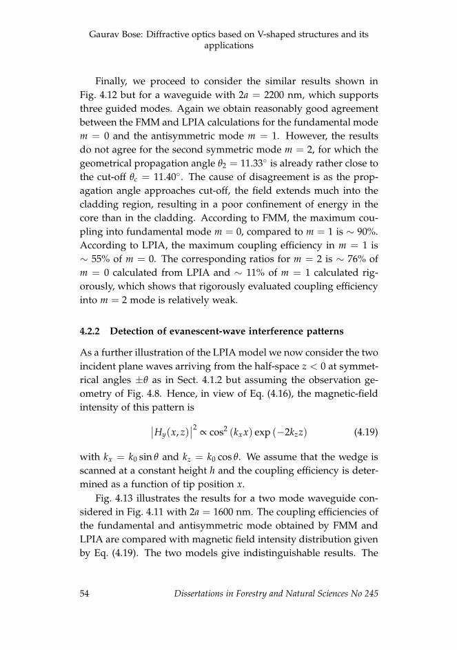
Gaurav Bose: Diffractive optics based on V-shaped structures and itsapplications
Finally, we proceed to consider the similar results shown in
Fig. 4.12 but for a waveguide with 2a = 2200 nm, which supports
three guided modes. Again we obtain reasonably good agreement
between the FMM and LPIA calculations for the fundamental mode
m = 0 and the antisymmetric mode m = 1. However, the results
do not agree for the second symmetric mode m = 2, for which the
geometrical propagation angle θ2 = 11.33◦ is already rather close to
the cut-off θc = 11.40◦. The cause of disagreement is as the prop-
agation angle approaches cut-off, the field extends much into the
cladding region, resulting in a poor confinement of energy in the
core than in the cladding. According to FMM, the maximum cou-
pling into fundamental mode m = 0, compared to m = 1 is ∼ 90%.
According to LPIA, the maximum coupling efficiency in m = 1 is
∼ 55% of m = 0. The corresponding ratios for m = 2 is ∼ 76% of
m = 0 calculated from LPIA and ∼ 11% of m = 1 calculated rig-
orously, which shows that rigorously evaluated coupling efficiency
into m = 2 mode is relatively weak.
4.2.2 Detection of evanescent-wave interference patterns
As a further illustration of the LPIA model we now consider the two
incident plane waves arriving from the half-space z < 0 at symmet-
rical angles ±θ as in Sect. 4.1.2 but assuming the observation ge-
ometry of Fig. 4.8. Hence, in view of Eq. (4.16), the magnetic-field
intensity of this pattern is
∣
∣Hy(x, z)∣
∣
2∝ cos2 (kxx) exp (−2kzz) (4.19)
with kx = k0 sin θ and kz = k0 cos θ. We assume that the wedge is
scanned at a constant height h and the coupling efficiency is deter-
mined as a function of tip position x.
Fig. 4.13 illustrates the results for a two mode waveguide con-
sidered in Fig. 4.11 with 2a = 1600 nm. The coupling efficiencies of
the fundamental and antisymmetric mode obtained by FMM and
LPIA are compared with magnetic field intensity distribution given
by Eq. (4.19). The two models give indistinguishable results. The
54 Dissertations in Forestry and Natural Sciences No 245

CHAPTER 4. LIGHT PROPAGATION IN WAVELENGTH SCALESTRUCTURES
30 35 40 45 50
0.2
0.4
0.6
0.8
1η
/η
max
α [deg]
(a)
30 35 40 45 50
0.2
0.4
0.6
0.8
1
η/
ηm
ax
α [deg]
(b)
30 35 40 45 50
0.2
0.4
0.6
0.8
1
η/
ηm
ax
α [deg]
(c)
Figure 4.12: Same as Fig. 4.10, but for a three-mode waveguide with 2a = 2200 nm.
(a) Fundamental mode m = 0. (b) First antisymmetric mode m = 1. (c) Second symmetric
mode m = 2 (adapted from Ref. [76]).
−300 −200 −100 0 100 200 300
0.2
0.4
0.6
0.8
1(a)
x [nm]
η/
ηm
ax,
I/I m
ax
−300 −200 −100 0 100 200 300
0.2
0.4
0.6
0.8
1(b)
x [nm]
η/
ηm
ax,
I/I m
ax
Figure 4.13: Observation of evanescent-wave interference patterns. Solid blue : magnetic-
field intensity given by Eq. (4.19). Normalized coupling efficiencies given by FMM (black
crosses) and LPIA (red circles) into (a) the fundamental mode m = 0 with α = 39.5◦ and
(b) the antisymmetric mode m = 1 with α = 41.8◦ (adapted from Ref. [76]).
Dissertations in Forestry and Natural Sciences No 245 55

Gaurav Bose: Diffractive optics based on V-shaped structures and itsapplications
results for the fundamental mode agree with Eq. (4.19). However,
since the planar waveguide is symmetric about the plane x = 0
(see Fig. 4.8) the mode solution are either even or odd in x. For
odd modes Hy(x, z) = −Hy(−x, z) is a solution, consequently in
the Fig. 4.13(b) there is a half a period phase shift between coupling
efficiency curves and the undisturbed interference pattern.
4.3 METALLIC GRATINGS WITH SUB-WAVELENGTH SLITS
Now we extend the discussion to plasmon waves and near-field op-
tics in the presence of metallic nanostructures. Similarly as above,
in the spirit of LPIA, diffraction effects in the incoupling process are
ignored. The geometrical approach is applied until the rays reach
the step-index waveguide, where its coupling to various guided
modes can be treated by the phase-matching approach (overlap in-
tegral). Hence, as usual in LPIA models, we move from the geomet-
rical optics picture to a wave optical model at the wedge-waveguide
interface. Making use of this quasi-geometrical approach as before,
we determine the optimum tip opening angle and compare the re-
sults of the geometrical model to rigorous simulations by the FMM.
4.3.1 Geometrical configuration and models
Figure 4.14 illustrates the geometrical configuration to be studied.
A homogeneous plane wave with wavelength λ is now assumed to
be normally incident at the interface z = 0 from the half space z < 0,
filled with a refractive index n. We assume a metallic (Al) grating
of height l, with very narrow slits, above the interface z = 0. Only
a TM-polarized wave can be transmitted efficiently through such
narrow slits [78]. Such a wave excites collective surface electron os-
cillations, known as plasmon oscillations, on both the entrance and
exit interfaces of the grating. Because of the geometrical symmetry,
two counter-propagating plasmonic waves are generated. Surface
plasmon interference then takes place in the wavelength-scale re-
gion above the grating [79–81], and we consider the observation
56 Dissertations in Forestry and Natural Sciences No 245

CHAPTER 4. LIGHT PROPAGATION IN WAVELENGTH SCALESTRUCTURES
x
ββαα
γ
φ
Al AlAl
z
n1
n2 n2
TM incidenceD
d
2a
l
x = 0z = 0
w
L
Figure 4.14: A schematic diagram of the y-invariant system considered here, showing ray
propagation into and inside a wedge with tip half-angle α connected to a waveguide of
width 2a.
of this interference pattern by inserting the tip-waveguide probe in
close proximity to the grating.
Let us first consider the inhomogeneous field associated with
just one of the two excited counter-propagating plasmons. Its sur-
faces of constant phase are planes close to (but coinciding with) the
direction of the surface normal. Hence one may associate a local
ray direction to the field, denoted by angle β in Fig. 4.14 [82]. In the
LPIA model we assume that one of the two plasmon waves arrives
from the left-hand-side of the wedge and the other from the right-
hand-side, these two waves being mutually fully correlated. The
inhomogeneous field arriving from the left is first refracted inside
the wedge through its left facet, and after total internal reflection
from the right-hand-side facet, coupled to the planar waveguide.
The plasmon field arriving from the right is treated similarly. The
theoretical LPIA analysis is a simple extension of that presented in
Sect. 4.1.1, the only difference being the inclusion of the angle β.
In the numerical simulations that follow, we consider wave-
length λ = 671.4 nm and assume that the metal is (bulk) aluminium
with complex refractive index 1.6231 + 8.0261i, and having a thick-
Dissertations in Forestry and Natural Sciences No 245 57

Gaurav Bose: Diffractive optics based on V-shaped structures and itsapplications
ness l = 70 nm. The grating period and slit width are taken as
d ∼ 12λ and w = 200 nm, and we choose a superperiod D ∼ 24λ
large enough to ensure that the non-periodic structure (including
the wedge and the waveguide) is modeled correctly. The rigor-
ous results are obtained using FMM with the S-matrix algorithm to
evaluate the coupling efficiencies into the waveguide modes [83].
Figure 4.15(a) illustrates the magnetic-field intensity in the grat-
ing region and the homogeneous spaces around it, without the
wedge being present. In order to see the surface wave intensity
pattern on the front side of the grating (z < 0) we have subtracted
the incident zeroth-order field before computing the intensity pat-
tern. Figure 4.15(b) shows the time-average Poynting vector for the
same configuration. Surface plasmons are seen on both the entrance
and the exit sides of the metallic grating, but our point of interest is
to detect the surface plasmons on the exit side of the grating, which
finally couple to the planar waveguide through the wedge.
4.3.2 Coupling efficiencies by rigorous theory and the geometri-
cal phase matching model
Let us first compare the coupling efficiencies predicted by LPIA
and by FMM as a function of the wedge angle α. In the examples
we keep the core width 2a of the waveguide constant, considering
0 200 400 600
−8000
−6000
−4000
−2000
0
2000
4000
6000
8000 0
0.2
0.4
0.6
0.8
1(a)
z [nm]
D[n
m]
−100 −50 0 50 100 150 200
3800
4000
4200
0
0.1
0.2
0.3
0.4
0.5(b)
z [nm]
D[n
m]
Figure 4.15: (a) Magnetic field intensity∣
∣Hy
∣
∣
2in and around the grating. (b) A closer
look at the direction of energy flow in the slit region, given by the Poynting vector.
58 Dissertations in Forestry and Natural Sciences No 245
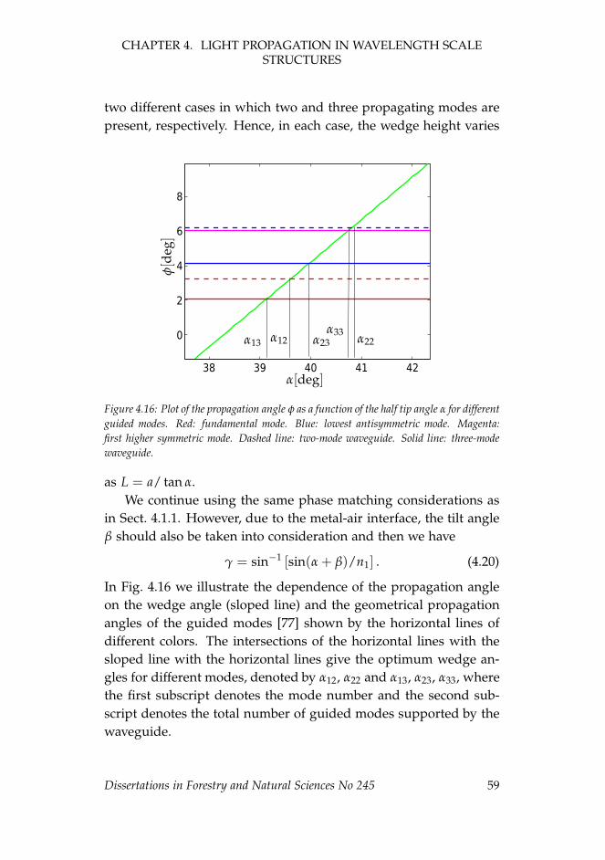
CHAPTER 4. LIGHT PROPAGATION IN WAVELENGTH SCALESTRUCTURES
two different cases in which two and three propagating modes are
present, respectively. Hence, in each case, the wedge height varies
38 39 40 41 42
0
2
4
6
8
α13 α12 α23
α33α22
α[deg]
φ[d
eg]
Figure 4.16: Plot of the propagation angle φ as a function of the half tip angle α for different
guided modes. Red: fundamental mode. Blue: lowest antisymmetric mode. Magenta:
first higher symmetric mode. Dashed line: two-mode waveguide. Solid line: three-mode
waveguide.
as L = a/ tan α.
We continue using the same phase matching considerations as
in Sect. 4.1.1. However, due to the metal-air interface, the tilt angle
β should also be taken into consideration and then we have
γ = sin−1 [sin(α + β)/n1] . (4.20)
In Fig. 4.16 we illustrate the dependence of the propagation angle
on the wedge angle (sloped line) and the geometrical propagation
angles of the guided modes [77] shown by the horizontal lines of
different colors. The intersections of the horizontal lines with the
sloped line with the horizontal lines give the optimum wedge an-
gles for different modes, denoted by α12, α22 and α13, α23, α33, where
the first subscript denotes the mode number and the second sub-
script denotes the total number of guided modes supported by the
waveguide.
Dissertations in Forestry and Natural Sciences No 245 59

Gaurav Bose: Diffractive optics based on V-shaped structures and itsapplications
Figure 4.17 renders the results for a two-mode waveguide with
parameters n1 = 1.52, n2 = 1.51, and 2a = 2800 nm. The coupling
efficiency curves evaluated by FMM are normalized to their respec-
tive maximum values. In view of FMM, we obtain maximum cou-
pling at a certain optimum wedge angle α. The upward-pointing
arrow in Fig. 4.17 corresponds to the values of α for which the an-
gle φ in Fig. 4.14 matches the geometrical propagation angle of the
fundamental mode. These optimum wedge angles are nearly the
same according to FMM and the geometrical phase matching con-
dition.
32 34 36 38 40 42 44 46 48
0.1
0.2
0.3
0.4
0.5
0.6
0.7
0.8
0.9
1
α12
(a)
α [deg]
η/
ηm
ax
32 34 36 38 40 42 44 46 48
0.2
0.3
0.4
0.5
0.6
0.7
0.8
0.9
1
α22
(b)
α [deg]
η/
ηm
ax
Figure 4.17: Rigorously evaluated coupling efficiencies into a two-mode waveguide as
a function of wedge half-angle α and comparison with the geometrical phase matching
condition (shown by arrows). (a) Fundamental mode m = 0. (b) Lowest antisymmetric
mode m = 1.
Figure 4.18 illustrates corresponding results for a waveguide
with 2a = 5000 nm and three propagating modes. The agreement
between FMM and phase matching condition (shown by arrows) is
good for the fundamental mode and antisymmetric mode as shown
in Fig. 4.18(a) and Fig. 4.18(b), respectively. As in Sect. 4.2.1, we ob-
serve a disagreement for the second symmetric mode m = 2, for
which the geometrical propagation angle φ = 6.0622◦ is again close
to the cutoff at φc = 7.25◦.
60 Dissertations in Forestry and Natural Sciences No 245

CHAPTER 4. LIGHT PROPAGATION IN WAVELENGTH SCALESTRUCTURES
32 34 36 38 40 42 44 46 48
0.1
0.2
0.3
0.4
0.5
0.6
0.7
0.8
0.9
1
α13
(a)
α [deg]
η/
ηm
ax
32 34 36 38 40 42 44 46 48
0.2
0.3
0.4
0.5
0.6
0.7
0.8
0.9
1
α23
(b)
α [deg]
η/
ηm
ax
32 34 36 38 40 42 44 46 480.2
0.3
0.4
0.5
0.6
0.7
0.8
0.9
1
α33
(c)
α [deg]
η/
ηm
ax
Figure 4.18: Same as Fig. 4.17 but for a three-mode waveguide. (a) Fundamental mode
m = 0. (b) Lowest antisymmetric mode m = 1. (c) Symmetric mode m = 2.
4.3.3 Examples of field patterns within the structure
Let us now take a brief detour by considering, instead of a nor-
mally incident plane wave, obliquely incident illumination of a thin
Al film (thickness 20 nm) at an angle θ = 48◦ and wavelength
λ = 671 nm. In this case the plasmon field propagates only in
the positive x-direction and no plasmon interference pattern is gen-
erated. However, the incoupling process can be illustrated quite
clearly in this geometry.
Figure 4.19 shows the distribution of the real part of the mag-
netic field for several different wedge angles of the waveguide tip
for a fixed L = 2000 nm. The height of the wedge is kept constant
in each case. So, with increase in α, the diameter 2a increases and
Dissertations in Forestry and Natural Sciences No 245 61
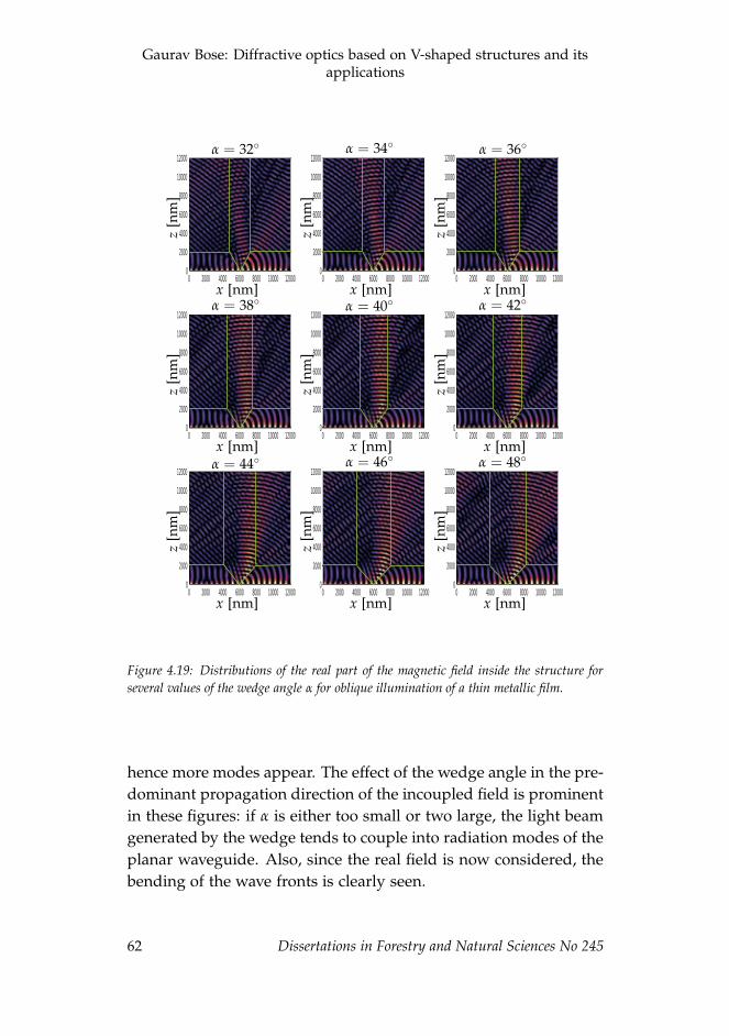
Gaurav Bose: Diffractive optics based on V-shaped structures and itsapplications
0 2000 4000 6000 8000 10000 120000
2000
4000
6000
8000
10000
12000
0 2000 4000 6000 8000 10000 120000
2000
4000
6000
8000
10000
12000
0 2000 4000 6000 8000 10000 120000
2000
4000
6000
8000
10000
12000
0 2000 4000 6000 8000 10000 120000
2000
4000
6000
8000
10000
12000
0 2000 4000 6000 8000 10000 120000
2000
4000
6000
8000
10000
12000
0 2000 4000 6000 8000 10000 120000
2000
4000
6000
8000
10000
12000
0 2000 4000 6000 8000 10000 120000
2000
4000
6000
8000
10000
12000
0 2000 4000 6000 8000 10000 120000
2000
4000
6000
8000
10000
12000
0 2000 4000 6000 8000 10000 120000
2000
4000
6000
8000
10000
12000
α = 32◦ α = 34◦ α = 36◦
α = 38◦ α = 40◦ α = 42◦
α = 44◦ α = 46◦ α = 48◦
x [nm]x [nm]x [nm]
x [nm]x [nm]x [nm]
x [nm]x [nm]x [nm]
z[n
m]
z[n
m]
z[n
m]
z[n
m]
z[n
m]
z[n
m]
z[n
m]
z[n
m]
z[n
m]
Figure 4.19: Distributions of the real part of the magnetic field inside the structure for
several values of the wedge angle α for oblique illumination of a thin metallic film.
hence more modes appear. The effect of the wedge angle in the pre-
dominant propagation direction of the incoupled field is prominent
in these figures: if α is either too small or two large, the light beam
generated by the wedge tends to couple into radiation modes of the
planar waveguide. Also, since the real field is now considered, the
bending of the wave fronts is clearly seen.
62 Dissertations in Forestry and Natural Sciences No 245

CHAPTER 4. LIGHT PROPAGATION IN WAVELENGTH SCALESTRUCTURES
2000 3000 4000 5000 6000
2
4
6
8
10
x 10−3
x [nm]
η(x),
I(x)
(a)
2000 3000 4000 5000 6000
1
2
3
4
5
6
7
x 10−3
x [nm]
η(x),
I(x)
(b)
2000 3000 4000 5000 6000
2
4
6
8
10
x 10−4
x [nm]
η(x),
I(x)
(c)
2000 3000 4000 5000 6000
1
2
3
4
x 10−3
x [nm]
η(x),
I(x)
(d)
Figure 4.20: Observation of surface plasmon interference. Red: magnetic field intensity
in the absence of the wedge. Black: coupling efficiency into the waveguide. (a) Sum of all
modes. Coupling efficiency into (b) the fundamental mode m = 0, (c) lowest antisymmetric
mode m = 1, and (d) symmetric mode m = 2.
4.3.4 Observation of surface plasmon interference
We are now returning to consider normally incident illumination
of the grating from the half-space z < 0. Due to the counter-
propagating surface plasmons, an interference pattern is formed
above the grating surface in the half-space z > l. We assume that
the wedge probes this pattern at h = 10 nm above the grating sur-
face and determine the coupling efficiency into the waveguide as a
function of the tip position x using FMM. The waveguide parame-
ters are those of the three-mode case in Fig. 4.18.
Figure 4.20(a) shows a comparison of the coupling efficiency
η(x) into the waveguide with the field intensity I(x) =∣
∣Hy(x)∣
∣
2in
the absence of the tip at a distance of 10 nm from the exit side of
the grating. The black line illustrates the total coupling efficiency
Dissertations in Forestry and Natural Sciences No 245 63

Gaurav Bose: Diffractive optics based on V-shaped structures and itsapplications
as the sum of all the propagating modes and the red line gives
the undisturbed field intensity. The maxima of the two curves are
normalized equal for easy comparison. The overall coupling effi-
ciency gives a rough estimate of the free-field intensity, although
the central maximum (due to the directly transmitted field through
the slit) appears remarkably high in proportion to that of the undis-
turbed plasmon-wave interference pattern. However, the locations
of the minima and maxima are not in perfect agreement. To clarify
the reason for this effect we investigate the modal contributions to
the total coupling efficiency, assuming wedge angles optimized for
the mode in question as discussed in Sect. 4.3.2. Figure 4.20(b)–(d)
show the results for the modes m = 0, m = 1, and m = 2, respec-
tively. Since the planar waveguide is symmetric about the plane
x = 0 as considered in Fig. 4.14, modes m = 0 and m = 2 are even
and mode m = 1 is odd in x. For odd modes Hy(x, z) = −Hy(−x, z)
is a solution, which results in half a period phase shift between the
coupling efficiency curve and the undisturbed interference pattern
as shown in Fig. 4.20(c). The contribution from the antisymmetric
mode thus gives rise to the distortion in the interference pattern in
Fig. 4.20(a).
4.4 DETECTION OF EVANESCENT FIELDS ABOVE BINARY
SUBWAVELENGTH GRATINGS
As a final example, we examine a case similar to that of Sect. 4.3.1,
assuming however a subwavelength-period grating of height l above
the interface z = 0. We consider both dielectric and metallic grat-
ings, and in all examples choose the parameters λ = 671 nm,
n = 1.456, n1 = 1.52, n2 = 1.51, and 2a = 2200 nm. The refrac-
tive index of the grating material is chosen as 1.456 in the dielectric
case and as 1.6231 + 8.0261i in the metallic case. The illumination
from the substrate is at an angle of incidence θ = 48◦ that exceeds
the critical angle at the interface z = 0. Moreover, the grating period
d is chosen small enough to prevent the generation of any propagat-
ing diffraction orders above the grating. Thus the field generated
64 Dissertations in Forestry and Natural Sciences No 245

CHAPTER 4. LIGHT PROPAGATION IN WAVELENGTH SCALESTRUCTURES
Scanning
λθ
n = n1
Weak field
x
z
d
L
0l
Cladding Cladding2a
α
Figure 4.21: Schematic diagram illustrating the evanescent-field detection above a
subwavelength-period grating by the SNOM tip.
above the plane z = l is a superposition of many evanescent diffrac-
tion orders and shows lateral structure in the absence of the tip. We
detect this evanescent field at the exit side of the grating at a fixed
scanning height h = 10 nm and compare it with the undisturbed
field intensity at the same height. Figure 4.21 shows a schematic
diagram of the geometry.
Figure 4.22 illustrates the fields inside and near the gratings,
without the tip being present. A dielectric grating with period
d = 250 nm is considered in Fig. 4.22(a) for TE polarized illumi-
nation and in Fig. 4.22(b) for TM polarized illumination. Inside the
grating, the electric-field amplitude is concentrated within the di-
electric ridges and in TM polarization in the air grooves, and the
evanescent fields appears somewhat stronger in TE than in TM po-
Dissertations in Forestry and Natural Sciences No 245 65

Gaurav Bose: Diffractive optics based on V-shaped structures and itsapplications
0 100 200 300 400 500
0
100
200
300
400
500
600
7000
0.5
1
1.5
2
2.5
z [nm]
x[n
m]
(a)
0 100 200 300 400 500
0
100
200
300
400
500
600
7000
0.5
1
1.5
2
2.5
z [nm]
x[n
m]
(b)
0 100 200 300 400 500
0
100
200
300
400
500
600
7000
0.2
0.4
0.6
0.8
1
z [nm]
x[n
m]
(c)
0 100 200 300 400 500
0
100
200
300
400
500
600
7000
0.2
0.4
0.6
0.8
1
z [nm]
x[n
m]
(d)
Figure 4.22: Distributions of (a) the electric field amplitude∣
∣Ey(x, z)∣
∣ in TE polarization
and (b) the magnetic field amplitude∣
∣Hy(x, z)∣
∣ in TM polarization inside and near the
binary dielectric grating. Correspondingly, (c) and (d) show the distributions of the same
quantities for a metallic binary grating.
larization (however, it should be stressed that we are plotting the
same quantity in these two cases). In the case of metallic gratings,
the polarization dependence is far more obvious. For TE illumina-
tion in the metallic case, the effective refractive index of the lowest-
order Bloch mode in the grating region is well known to have a large
imaginary part and therefore light can not penetrate deep into the
air grooves. This is seen clearly in Fig. 4.22(c). In the case of TM
polarization, however, the imaginary part of the Bloch mode is sub-
stantially smaller. Extraordinary transmission of light though the
grating takes place as seen in Fig. 4.22(d). Thus the metallic grating
becomes nearly transparent and a strong inhomogeneous field is
generated on its exit side.
Figure 4.23 shows a closer look at the magnitude and the local
66 Dissertations in Forestry and Natural Sciences No 245

CHAPTER 4. LIGHT PROPAGATION IN WAVELENGTH SCALESTRUCTURES
direction of energy flow in the binary metallic grating for TM illu-
mination given by the time-averaged Poynting vector. We observe
a counter-clockwise rotation of energy flow around the metallic
block, though one should be rather careful with such interpreta-
tions in the subwavelength scale. Nevertheless, the Poynting vector
in the half-space above the grating points consistently in the neg-
ative z-direction, indicating a plasmon wave propagating in this
direction for the parameters chosen here. Let us now introduce
the tip-waveguide probe and compare the coupling efficiency with
the intensity of the undisturbed field. Figure 4.24 shows such a
comparison for TM illumination of a dielectric grating at a large
angle of incidence at θ = 70◦. In the FMM analysis we repeated
the subwavelength period of 250 nm by 80 times to create a compu-
tation window with superperiod 20000 nm, which is large enough
to contain also the probe. Figure 4.24(a) shows the comparison for
the fundamental mode and Fig. 4.24(b) for the first anti-symmetric
mode. In the latter case we again see a half-phase shift between
the observed and the undisturbed patterns. The results of a similar
0 100 200 300
400
500
600
700
800
0
0.05
0.1
0.15
0.2
0.25
0.3
0.35
0.4
z[nm]
x[n
m]
Figure 4.23: Distribution of the magnitude and local direction of the time-averaged Poynt-
ing vector in and near a metallic binary grating. Here λ = 671.4 nm, d = 620 nm, and
θ = 50◦ .
Dissertations in Forestry and Natural Sciences No 245 67

Gaurav Bose: Diffractive optics based on V-shaped structures and itsapplications
300 400 500 600 700 800
2
4
6
8
10
x 10−5 (a)
x [nm]
η(x),
I(x)
300 400 500 600 700 8000
2
4
6
8
x 10−5 (b)
x [nm]
η(x),
I(x)
Figure 4.24: Observation of fields above a binary dielectric subwavelength grating. Red:
Magnetic field intensity. Black: coupling efficiency. (a) Fundamental mode m = 0.
(b) Anti-symmetric mode m = 1.
analysis for a binary metallic grating are shown in Fig. 4.25.
200 300 400 500 600 700 800
2
4
6
8
10
x 10−5 (a)
x [nm]
η(x),
I(x)
200 300 400 500 600 700 800
2
4
6
8
10x 10
−5 (b)
η(x),
I(x)
x [nm]
Figure 4.25: Same as Fig. 4.24 but for a binary metallic subwavelength grating.
4.5 SUMMARY
We have introduced a geometrical optics based local-plane-interface
approach to model near field phenomena involving interactions of
evanescent, inhomogeneous, and plasmon waves with wavelength-
scale scatterers. In particular, a model for wedge-based scanning
near-field microscope with a bare tip was developed and applied
to observation of near fields behind different types of gratings. The
results were compared to a rigorous model based on the Fourier
68 Dissertations in Forestry and Natural Sciences No 245

CHAPTER 4. LIGHT PROPAGATION IN WAVELENGTH SCALESTRUCTURES
modal method, and fair agreement was reached in many cases. The
coupling efficiencies did not match perfectly since the geometri-
cal model ignores diffraction effects within the wedge region. The
results obtained (especially the diffraction patterns in the absence
of the waveguide) could probably be improved by including the
boundary diffraction wave created by the tip edge. Additionally,
the inclusion of the evanescent field on the second (reflecting) sur-
face of the wedge in the geometrical analysis could also improve
significantly the diffraction pattern at the output plane of the wedge
but these remains the topic of future research.
Dissertations in Forestry and Natural Sciences No 245 69

Gaurav Bose: Diffractive optics based on V-shaped structures and itsapplications
70 Dissertations in Forestry and Natural Sciences No 245

5 Coding of high-frequency
carrier V-shape gratings
Diffractive optics is a versatile technology to create optical elements
with complex functionality. The first computational coding scheme
to create diffractive elements from mathematically defined signals
(computer-generated holography) was introduced by Lohmann [84].
Other schemes soon followed, such as the phase-only (kinoform)
coding technique put forward by Lesem, Hirsch, and Jordan [85].
Yet another approach emerged, which is based on modulation of
high-frequency carrier gratings and has its origin in off-axis op-
tical holography [86]. By the early 1990’s, the synthesis methods
in diffractive optics had been developed to a level, which allowed
the design of high-quality, high-efficiency elements using iterative
techniques [87]. By this era the development of microlithographic
fabrication techniques also permitted the encoding of diffractive
elements in different types of wavelength-scale carrier structures.
Coding methods that employ wavelength-scale nanostructures de-
signed by rigorous diffraction theory [5] are now commonplace,
and their fabrication is feasible using modern nanolithography [88,
89].
Coding methods that employ high-frequency carrier gratings
and involve modulation of the larger-scale structure of the element
are of substantial interest. In early studies [26–28] binary grat-
ings were used as carriers, providing high transmission-mode or
reflection-mode efficiency when the carrier period, groove depth
and width, and the angle of incidence are chosen properly. In
the transmission mode such elements feature rather high input-
angle selectivity of the diffraction efficiency, but in the reflection
mode high efficiency can be maintained over a much wider angular
range [27].
Dissertations in Forestry and Natural Sciences No 245 71

Gaurav Bose: Diffractive optics based on V-shaped structures and itsapplications
In this chapter, we propose a new method to realize high-carrier-
frequency diffractive elements, which is based on using V-shaped
carrier gratings as an alternative to binary resonance-domain grat-
ings. In terms of optical performance, these two approaches are
comparable especially in the reflection mode. However, the sil-
icon wet etching technique [90] of V-shaped structures facilitates
precise control of the groove shape and easy replication. Regular
V-gratings have been used in, e.g., spectroscopy [91–93], infrared
beam splitting [94, 95], reflection suppression [96, 97], and optical
interconnection [98]. Recently, wet etching of silicon has triggered
a new era in the production of photovoltaic devices [16, 99, 100].
At first we introduce several general techniques for the real-
ization of diffractive structures by modulation of the high-carrier-
frequency V-gratings. Corresponding methods based on modula-
tion of the local groove position or width have been introduced for
binary gratings in the past; see, e.g., Refs. [101, 102]. We also dis-
cuss the limitations of the new coding schemes. Then we proceed
to design profiles that are capable of splitting an incident beam
into several output beams of equal efficiency. Such array illumi-
nators are among the most important diffractive elements, and in
addition they are easy to characterize both theoretically and exper-
imentally. We apply rigorous diffraction theory to study conditions
under which good signal quality can be achieved. An experimen-
tal demonstration is provided by patterning the modulated grating
structure using electron beam lithography, wet etching it in silicon,
replicating it in polymer, and coating the replicated structure with
a thin metal layer.
High-frequency carrier techniques used in diffractive optics can
be divided into two main categories: on-axis and off-axis coding
techniques. In the on-axis schemes discussed in Sect. 5.1 one makes
use of the zeroth diffraction order of a subwavelength-period car-
rier grating. The local material volume fill factor is varied from
one period of the carrier grating to another, which results in mod-
ulation of the effective refractive index of the grating and thereby
in phase modulation of the output field. In off-axis schemes one
72 Dissertations in Forestry and Natural Sciences No 245

CHAPTER 5. CODING OF HIGH-FREQUENCY CARRIER V-SHAPEGRATINGS
uses a higher order (typically first) of the carrier grating and mod-
ulates the phase of the incident field by varying the groove/ridge
positions. This scheme is discussed in Sect. 5.2.
5.1 V-GROOVE WIDTH MODULATION
Let us start by considering the encoding of the phase information of
the wavefront into a high-frequency carrier, making use of groove-
width variations. This scheme was introduced for binary gratings
independently by Farn [103] and Stork et al. [104]. It is based on
modulating the fill factor of a binary subwavelength-period grating
as a function of position to encode the desired continuous phase-
delay profile φ(x) of a paraxial-domain diffractive element (we con-
sider, for simplicity of illustration, only y-invariant optical functions
in this chapter).
Figure 5.1 illustrates the principle of groove width modulation
of a high-frequency-carrier V-grating. Here the simplest example of
a linear phase function φ(x) = cx, where c is a constant, is consid-
ered. The period of the carrier grating is taken as d < λ, and the
volume fraction of the material is controlled by varying the groove
width w as a function of position. Since α is constant, varying w also
leads to groove-depth modulation. In order for this coding method
to work, the values of φ(x) must be reduced to the interval [0, 2π),
which is always possible (for monochromatic light). Now the idea
is to map the values of φ(x) to values of w at an equally spaced
grid of sampling points separated by d, which results in a profile of
the type shown in Fig. 5.1(b). Note that the higher the value of c is,
the smaller is the number of sampling points of φ(x) in the [0, 2π)
interval. In order to keep the local diffraction efficiency of the mod-
ulated element at a sufficiently high level, this number should be at
least four (as it is in Fig. 5.1).
Rigorous FMM analysis is available to determine the mapping
between the groove width and the resulting phase delay. Because
of fabrication constraints in Si wet etching, one should ensure that
the widths d − w of all flat regions are at least ∼ 50 nm. With
Dissertations in Forestry and Natural Sciences No 245 73

Gaurav Bose: Diffractive optics based on V-shaped structures and itsapplications
2π
x
z
d
dw
αAir
COC
(a)
(b)
λ
φ
0
0
Figure 5.1: Groove width modulation. (a) Phase modulation showing four-level quanti-
zation between phase values 0 and 2π (b) Schematic diagram showing the groove width
modulated structure with four different phase values.
this constrain in mind, we aim to optimize w to obtain maximum
efficiency in the zeroth order and, at the same time, achieve a max-
imum phase delay of at least 2π radians. To this end we scan w
by using FMM with the S-matrix propagation algorithm to evalu-
ate the diffraction efficiencies. As illustrated in Fig. 3.2, the wedge
region is again divided into J layers thin enough to model the con-
tinuous facets with sufficient accuracy. Typically we now choose
J = 50 and include ∼ 100 Floquet–Bloch modes in the calculation
of carrier-grating efficiencies.
5.1.1 Transmission-type groove width modulation
We consider first the optimization of the carrier-grating structure
in the transmission case. The V-groove apex half-angle is assumed
to be α = 35.26◦ and we consider two design wavelengths, λ0 =
457 nm and λ0 = 533 nm. The material on the incident side is
Cyclo Olefin Copolymer (COC) with refractive index n = 1.52. In
74 Dissertations in Forestry and Natural Sciences No 245

CHAPTER 5. CODING OF HIGH-FREQUENCY CARRIER V-SHAPEGRATINGS
0 200 4000
0.2
0.4
0.6
0.8
1
w [nm]
η0
(a)
0 200 400 6000
1
2
3
4
5
(b)
w [nm]
φ[r
ad]
Figure 5.2: Groove width modulation for transmission type gratings. (a) Plots of zeroth
order efficiency and (b) the phase delay as a function of groove width w for periods d =
457 nm (blue) and d = 533 nm (red). The solid lines show the results for TM incident
light and the dashed lines for TE incident light.
Fig. 5.2(a) we plot the zeroth-order efficiency as a function of w up
to w = d. The efficiency for TM-polarized incident light (shown by
solid lines) is remarkably high, but in TE polarization the results
are far less satisfactory. On the other hand, as shown in Fig. 5.2(b),
the maximum phase delay that can be obtained is 1.65π radians,
which is almost 0.35π radians less than what is ideally desired.
Due to the insufficient phase delay, the full phase function cannot
be coded perfectly into the carrier grating profile. Equally-spaced
four-level coding still appears possible at first sight since it only
requires phase delays up to 1.5π radians. However, in transmission-
type optics the phase delay is evaluated at the deepest apex level
of the entire modulated structure, not only between the apex and
the top level of the carrier grating. This implies an extra phase due
to propagation through the homogeneous section of the material,
which severely reduces the available phase coding range. Hence, in
practise, it is not possible to code arbitrary phase profiles properly
in transmission-type V-carrier gratings.
5.1.2 Reflection-type groove width modulation
After the failure of transmission-type gratings we proceed to con-
sider the case of optimizing reflection-type gratings. We consider a
Dissertations in Forestry and Natural Sciences No 245 75
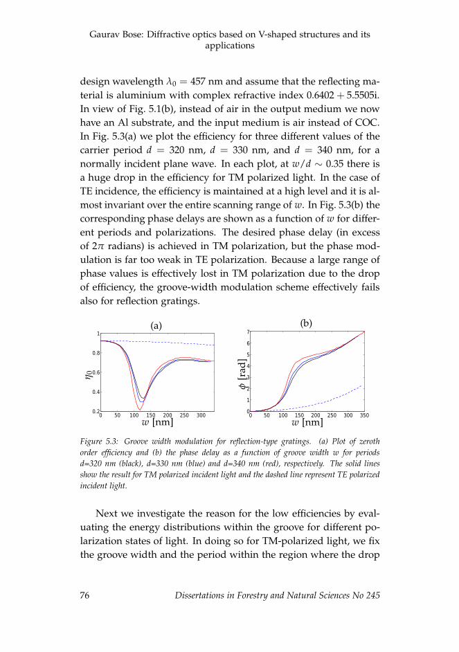
Gaurav Bose: Diffractive optics based on V-shaped structures and itsapplications
design wavelength λ0 = 457 nm and assume that the reflecting ma-
terial is aluminium with complex refractive index 0.6402 + 5.5505i.
In view of Fig. 5.1(b), instead of air in the output medium we now
have an Al substrate, and the input medium is air instead of COC.
In Fig. 5.3(a) we plot the efficiency for three different values of the
carrier period d = 320 nm, d = 330 nm, and d = 340 nm, for a
normally incident plane wave. In each plot, at w/d ∼ 0.35 there is
a huge drop in the efficiency for TM polarized light. In the case of
TE incidence, the efficiency is maintained at a high level and it is al-
most invariant over the entire scanning range of w. In Fig. 5.3(b) the
corresponding phase delays are shown as a function of w for differ-
ent periods and polarizations. The desired phase delay (in excess
of 2π radians) is achieved in TM polarization, but the phase mod-
ulation is far too weak in TE polarization. Because a large range of
phase values is effectively lost in TM polarization due to the drop
of efficiency, the groove-width modulation scheme effectively fails
also for reflection gratings.
0 50 100 150 200 250 3000.2
0.4
0.6
0.8
1
w [nm]
η0
(a)
0 50 100 150 200 250 300 3500
1
2
3
4
5
6
7(b)
w [nm]
φ[r
ad]
Figure 5.3: Groove width modulation for reflection-type gratings. (a) Plot of zeroth
order efficiency and (b) the phase delay as a function of groove width w for periods
d=320 nm (black), d=330 nm (blue) and d=340 nm (red), respectively. The solid lines
show the result for TM polarized incident light and the dashed line represent TE polarized
incident light.
Next we investigate the reason for the low efficiencies by eval-
uating the energy distributions within the groove for different po-
larization states of light. In doing so for TM-polarized light, we fix
the groove width and the period within the region where the drop
76 Dissertations in Forestry and Natural Sciences No 245

CHAPTER 5. CODING OF HIGH-FREQUENCY CARRIER V-SHAPEGRATINGS
in efficiency occurs. We illustrate in Fig. 5.4(a) distributions of the
time-averaged Poynting vector, with arrows for direction and colors
for magnitude as before. It seems evident from these results that, in
the case of TM incidence, two counter-propagating plasmon waves
propagating in ±x directions are excited, which results in the drop
of the TM efficiency for the zeroth reflected order due to absorption
in the grating material. Qualitatively similar behavior, confirmed
by our calculations, is observed also for binary reflection-type grat-
ings [105].
The interpretation of Fig. 5.4(b), which illustrates the case of
TE polarized incident light, is even simpler: light cannot penetrate
deep inside the grooves of the metallic subwavelength-period grat-
ing, which causes the insufficient phase delay seen in Fig. 5.3(b).
This explains, at least qualitatively, the nearly flat efficiency curve
in Fig. 5.3(a). Having again arrived at discouraging results, we pro-
ceed look for another coding scheme, which we discuss in the fol-
lowing section.
−50 0 50 100
−100
−50
0
50
100 0
0.1
0.2
0.3
0.4
0.5
z [nm]
x[n
m]
(a)
−50 0 50
−100
−50
0
50
100 0
0.02
0.04
0.06
0.08
0.1
z [nm]
x[n
m]
(b)
Figure 5.4: The direction of energy flow given by the time-averaged Poynting vector for
(a) TM polarization and (b) TE polarization of the incident light. Here λ = 457 nm,
w = 120 nm, and d = 340 nm. Only the reflected part of the field is considered here.
5.2 V-RIDGE POSITION MODULATION
The idea behind off-axis coding of high-frequency carrier gratings
is essentially similar to Lohmann’s detour-phase principle. If the
entire grating is moved sideways in the x-direction with respect to
Dissertations in Forestry and Natural Sciences No 245 77
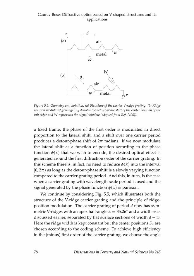
Gaurav Bose: Diffractive optics based on V-shaped structures and itsapplications
z d
air
metal
metal w
w
Sn
θ
air
W
D x
(a)
(b)
Figure 5.5: Geometry and notation. (a) Structure of the carrier V-ridge grating. (b) Ridge
position modulated gratings: Sn denotes the detour-phase shift of the center position of the
nth ridge and W represents the signal window (adapted from Ref. [106]).
a fixed frame, the phase of the first order is modulated in direct
proportion to the lateral shift, and a shift over one carrier period
produces a detour-phase shift of 2π radians. If we now modulate
the lateral shift as a function of position according to the phase
function φ(x) that we wish to encode, the desired optical effect is
generated around the first diffraction order of the carrier grating. In
this scheme there is, in fact, no need to reduce φ(x) into the interval
[0, 2π) as long as the detour-phase shift is a slowly varying function
compared to the carrier-grating period. And this, in turn, is the case
when a carrier grating with wavelength-scale period is used and the
signal generated by the phase function φ(x) is paraxial.
We continue by considering Fig. 5.5, which illustrates both the
structure of the V-ridge carrier grating and the principle of ridge-
position modulation. The carrier grating of period d now has sym-
metric V-ridges with an apex half-angle α = 35.26◦ and a width w as
discussed earlier, separated by flat surface sections of width d − w.
Here the ridge width is kept constant but the center positions Sn are
chosen according to the coding scheme. To achieve high efficiency
in the (minus) first order of the carrier grating, we choose the angle
78 Dissertations in Forestry and Natural Sciences No 245

CHAPTER 5. CODING OF HIGH-FREQUENCY CARRIER V-SHAPEGRATINGS
of incidence θ and the carrier period d in such a way that the only
propagating reflected orders are m = −1 and m = 0. We then op-
timize w to obtain maximum efficiency η−1 in order m = −1. We
further assume that
sin θ =λ0
2d. (5.1)
This is in fact the Bragg condition (or the condition for Littrow
mounting) for the first diffraction order at design wavelength λ0.
Again we scan w, using FMM with the S-matrix propagation algo-
rithm to evaluate the diffraction efficiencies.
5.2.1 Reflection type ridge-position modulation
In what follows, we consider reflection-type elements at a design
wavelength λ0 = 457 nm, assuming that the metal is (bulk) alu-
minium with complex refractive index n = 0.6402 + i5.5505. In the
present coding scheme we have some freedom to choose the carrier
period d and the angle of incidence θ. In Fig. 5.6 we plot carrier-
grating design results for three different values of the angle of in-
cidence, namely θ = 30◦, θ = 42◦, and θ = 60◦. The carrier period
is kept at a fixed value d = 340 nm. Remarkably, for all values of θ
considered, the optimum solution with η−1 ≈ 87% is achieved with
a ridge width w ≈ 220 nm and a fill factor w/d ≈ 0.64. This effi-
ciency is high since the reflectance of a flat air-aluminum interface
at these angles of incidence is in the range 86 − 91%. In fact, the
zeroth-order efficiency reduces close to zero at the optimum value
of η−1. In view of Fig. 5.6(b), the value of d is not critical: we obtain
essentially the same optimum η−1 at the same value of w as above
for all carrier periods d considered in Fig. 5.6.
The dashed lines in Fig. 5.6 show results for TE polarized light
with θ = 42◦ in Fig. 5.6(a) and d = 340 nm in Fig. 5.6(b). Now the
maximum efficiency is limited to ∼ 50%, at least if we leave some
room for position modulation. The reason for the low efficiency is
again that TE polarized light cannot penetrate deep into the grooves
of metallic subwavelength-period gratings, and this prevents us
from achieving sufficient phase modulation for high diffraction effi-
Dissertations in Forestry and Natural Sciences No 245 79

Gaurav Bose: Diffractive optics based on V-shaped structures and itsapplications
0 100 200 3000
0.2
0.4
0.6
0.8
1
θ=30°
θ=42°
θ=60°
θ=42° (TE)
w [nm]
η−
1
(a)
0 100 200 3000
0.2
0.4
0.6
0.8
1
d=330 nm d=340 nmd=350 nm d=340 nm (TE)
w [nm]
η−
1
(b)
Figure 5.6: Efficiency of carrier order m = −1 for (a) different incident angles and (b) dif-
ferent carrier periods when we vary the ridge width w. The solid and dashed lines refer to
TM and TE polarization, respectively (adapted from Ref. [106]).
ciency. At the wavelength and period considered here, Al is a good
plasmonic material. However, now the optimized grating period is
too small for plasmon resonance to be excited, and this one reason
why the coding method works.
Figure 5.7 illustrates the time-averaged Poynting vector for TM
polarized light in the structure. The fill factor w/d ≈ 0.64 of the
ridge and the angle of incidence θ = 42◦ are fixed to show the field
amplitude and the direction of the energy flow (arrows). Unlike
in groove-width modulation at normal incidence, here we do not
observe any evidence of surface plasmon resonance.
5.2.2 Coding of V-ridge structures
Let us again refer to Fig. 5.5, in which the modulation of the carrier
is determined by the shifts Sn of the ridge tips with respect to their
undisturbed positions xn = (n − 1/2)d of the carrier grating. Using
the detour-phase principle [84] these shifts are determined by the
phase-only modulation function φ(x) to be encoded in the element.
Denoting the sampled values of φ(x) at xn by φn, we have
Sn =φn · d
2π. (5.2)
The above φ(x) represents the modulation function, which is de-
signed to convert an incident plane wave into a predefined angu-
lar spectrum of plane waves within some on-axis signal window
80 Dissertations in Forestry and Natural Sciences No 245

CHAPTER 5. CODING OF HIGH-FREQUENCY CARRIER V-SHAPEGRATINGS
−100 0 100
−150
−100
−50
0
50
100
1500
0.02
0.04
0.06
0.08
0.1
z [nm]
x[n
m]
(a)
Figure 5.7: The direction of energy flow for Bragg’s incidence (shown in blue) and re-
flectance (shown in black arrows) in case of V ridge carrier grating given by the Poynting
vector for TM polarization of incident light. Here λ = 457 nm, w = 220 nm, and
d = 340 nm.
W [107]. After encoding, this W is shifted off-axis around the cho-
sen diffraction order of the carrier grating.
In the spirit of the position modulation scheme, φ(x) should
vary slowly relative to the carrier period in the sense that the con-
dition
|sn − sn+1| ≪ d (5.3)
holds for all n. If this condition holds, the adjacent ridges do not
overlap, except perhaps at points where the phase of φ(x) changes
abruptly. Such points occur inevitably if φ(x) is wrapped into the
[0, 2π] interval. However, in many designs one also encounters
phase jumps less than 2π radians, which cannot be unwrapped.
Nevertheless, we assume φ(x) to vary slowly enough to ensure that
these isolated phase jump points are sufficiently far apart to cause
only local disturbances in the coded profile.
In what follows we will consider periodic modulation functions
with period D, so that φ(x + D) = φ(x). We choose D to be an in-
teger multiple of the carrier period d, i.e., D = Nd as illustrated in
Fig. 5.5. Then the carrier order m = −1 splits into a discrete angular
Dissertations in Forestry and Natural Sciences No 245 81

Gaurav Bose: Diffractive optics based on V-shaped structures and itsapplications
spectrum of plane waves in the signal window W and correspond
to the diffraction orders of an on-axis element with phase function
φ(x). In order to satisfy the condition (5.3), the effective spread of
the angular spectrum within W must be small compared with the
diffraction angle of the carrier order m = −1. In other words, the
diffraction geometry should be parabasal. In the next section we
proceed to consider this case more quantitatively by giving numer-
ical examples.
5.2.3 Numerical examples
In this section we consider diffractive elements that divide the in-
cident plane wave into an array of Q plane waves with equal effi-
ciencies, propagating in different directions. Such elements are fre-
quently called beam splitters or array illuminators. We refer to the
index of the orders of the modulation grating by symbol q. Thereby
ηq denotes the diffraction efficiency of order q and the total effi-
ciency within the set W of signal orders is
η = ∑q∈W
ηq. (5.4)
Furthermore, the array uniformity error is defined as
E =max ηq − min ηq
max ηq + min ηq, (5.5)
with q ∈ W. Note that, after modulation of the carrier grating,
order q in the axial design corresponds to order q − N of the super-
periodic grating with period D.
With the help of FMM, we investigate the effect of N in the
performance of ridge-position modulated gratings. In all examples
considered here we take λ = 457 nm, θ = 42◦, and d = 340 nm. In
order to obtain good convergence, the number of diffraction orders
included in the FMM analysis is at least ∼ 30N. The bulk refractive
index of Al was used to model the metal substrate, assumed semi-
infinite as in Fig. 5.5.
82 Dissertations in Forestry and Natural Sciences No 245

CHAPTER 5. CODING OF HIGH-FREQUENCY CARRIER V-SHAPEGRATINGS
A triplicator is an element with Q = 3 equal-efficiency orders.
The optimum continuous profile φ(x) of a triplicator is known an-
alytically [108] and has a total efficiency η = 0.92556 into orders
q = −1, 0,+1 contained in W. Figure 5.8 illustrates the discrete
N = 16 bit design of φ(x), obtained by IFTA, and the resulting
on-axis diffraction pattern calculated within the thin-element ap-
proximation. The efficiency is η ≈ 0.926 and the array uniformity is
virtually perfect. The rest of the incident light goes to higher orders
since amplitude freedom must be allowed in the design.
5 10 150
1
2
3
n
φn
[rad
]
(a)
−5 0 50
0.1
0.2
0.3
q
ηq
(b)
Figure 5.8: (a) The continuous phase profile φ(x) of the triplicator and its discrete form
with N = 16 bits, shown by the sampled dots and vertical lines. (b) The efficiencies ηq
of the central orders q in the paraxial domain predicted by the thin-element approximation
(adapted from Ref. [106]).
Similarly, the continuous φ(x) for the case Q = 5 is shown in
Fig. 5.9(a). This design has a total efficiency of η = 0.921 into orders
q = −2, . . . ,+2. The diffraction pattern including some higher or-
ders is shown in Fig. 5.9(b). The average uniformity error predicted
by IFTA is E = 9.945× 10⁻⁷. As third example, the continuous φ(x)
for Q = 8 is shown in Fig. 5.9(c) and produces a total efficiency of
η = 0.96512 into orders q = −3, . . . ,+4. The diffraction pattern
is shown in Fig. 5.9(d), and the uniformity error given by IFTA is
E = 6.12 × 10⁻⁷.
Let us next consider an encoded triplicator with N = 16 bits.
We assume λ = 457 nm, θ = 42◦, and choose the carrier period
as d = 340 nm. The result shown in Fig. 5.10(a) is based on FMM
analysis. On comparing this result with Fig. 5.8(b) we see that the
array is somewhat distorted and there is some residual light in the
Dissertations in Forestry and Natural Sciences No 245 83

Gaurav Bose: Diffractive optics based on V-shaped structures and itsapplications
10 20 300
1
2
3
4
5
n
φn
[rad
]
(a)
−5 0 50
0.05
0.1
0.15
q
ηq
(b)
10 20 30−4
−2
0
2
4
n
φn
[rad
]
(c)
−5 0 50
0.02
0.04
0.06
0.08
0.1
0.12
q
ηq
(d)
Figure 5.9: (a) The continuous form of the phase profile φ(x) of the Q = 5 array illumi-
nator and its discrete N = 32 bit form. (b) The efficiencies ηq of the central orders q in the
paraxial domain for the 5-beam case. Similar plots for Q = 8 are shown in (c) and (d).
central region of the pattern. This axial noise is due to order m = 0
of the carrier grating, which is also the zeroth generalized order of
the modulated grating. It may be concluded that, at N = 16, the
geometry is not yet sufficiently parabasal to satisfy the condition
(5.3), which explains the large uniformity error. The array unifor-
mity is indeed improved if we increase N, as shown in Figs. 5.10(c)
and 5.10(d). This behaviour is analogous to observations for binary
carrier gratings [27]. Table 5.1 illustrates the results of the FMM
analysis more quantitatively. The diffraction efficiencies of the en-
coded elements are close to the expected value ∼ 80.6%, which is
the efficiency of the axial design (92.6%) given by IFTA, multiplied
by the rigorously calculated efficiency (87%) of the carrier grating.
A similar analysis is performed also for array illuminators that
generate five beams in orders q = −2, . . . ,+2 and eight beams in
orders q = −3, . . . , 4. IFTA predicts η ≈ 0.92 in the 5-beam case
and η ≈ 0.96 in the 8-beam case. In the case of triplicator, φ(x)
was limited within the [0, 2π) interval. In the case Q = 8 this in-
84 Dissertations in Forestry and Natural Sciences No 245

CHAPTER 5. CODING OF HIGH-FREQUENCY CARRIER V-SHAPEGRATINGS
−20 −15 −10 −5 00
0.05
0.1
0.15
0.2
0.25
q − N
ηq−
N
(a)
−18 −16 −140
0.05
0.1
0.15
0.2
0.25
q − N
ηq−
N
(b)
−34 −32 −300
0.05
0.1
0.15
0.2
0.25
q − N
ηq−
N
(c)
−66 −64 −620
0.05
0.1
0.15
0.2
0.25
q − N
ηq−
N
(d)
Figure 5.10: Rigorous analysis of encoded triplicators. (a) Efficiencies ηq of diffraction
orders of the N = 16 bit design. (b) A closer look around W. (c) Efficiencies of the
N = 32 bit design. (d) Efficiencies of the N = 64 bit design (adapted from Ref. [106]).
terval is exceeded but we first unwrapped φ(x), then shifted its
minimum to −π, and finally wrapped the profile again. In doing
so we minimize the number 2π phase jump to two. An unwrapped
profile contains one phase jump of π radians, which cannot be un-
wrapped. Tables 5.2 and 5.3 show quantitative results correspond-
ing to Table 5.1 for the Q = 5 and Q = 8 designs, respectively. As
expected, if we increase Q while keeping N constant, the uniformity
error increases. However, the uniformity again improves when N is
increased. We noticed that for the Q = 8 design, rewrapping φ(x)
somewhat unexpectedly improved the array uniformity.
5.2.4 Effects of varying the wavelength and angle of incidence
It is of substantial interest to examine the effects of the angle of inci-
dence of the input plane wave, as well as the wavelength sensitivity
of the designs at Bragg incidence. We concentrate here on the tripli-
cator case, but the other designs behave analogously. Figure 5.11(a)
Dissertations in Forestry and Natural Sciences No 245 85
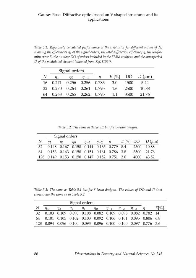
Gaurav Bose: Diffractive optics based on V-shaped structures and itsapplications
Table 5.1: Rigorously calculated performance of the triplicator for different values of N,
showing the efficiencies ηq of the signal orders, the total diffraction efficiency η, the unifor-
mity error E, the number DO of orders included in the FMM analysis, and the superperiod
D of the modulated element (adapted from Ref. [106]).
Signal orders
N η1 η0 η−1 η E [%] DO D (µm)
16 0.271 0.256 0.256 0.783 3.0 1500 5.44
32 0.270 0.264 0.261 0.795 1.6 2500 10.88
64 0.268 0.265 0.262 0.795 1.1 3500 21.76
Table 5.2: The same as Table 5.1 but for 5-beam designs.
Signal orders
N η2 η1 η0 η−1 η−2 η E [%] DO D (µm)
32 0.148 0.167 0.158 0.141 0.165 0.779 8.4 2500 10.88
64 0.153 0.163 0.158 0.151 0.161 0.786 3.8 3500 21.76
128 0.149 0.153 0.150 0.147 0.152 0.751 2.0 4000 43.52
Table 5.3: The same as Table 5.1 but for 8-beam designs. The values of DO and D (not
shown) are the same as in Table 5.2.
Signal orders
N η4 η3 η2 η1 η0 η−1 η−2 η−3 η E[%]
32 0.103 0.109 0.090 0.108 0.082 0.109 0.098 0.082 0.782 14
64 0.101 0.105 0.102 0.103 0.092 0.106 0.101 0.095 0.806 6.8
128 0.094 0.096 0.100 0.093 0.096 0.100 0.100 0.097 0.776 3.6
86 Dissertations in Forestry and Natural Sciences No 245

CHAPTER 5. CODING OF HIGH-FREQUENCY CARRIER V-SHAPEGRATINGS
shows the effect of varying the wavelength λ with a sampling inter-
val of 0.6 nm. The efficiency of the signal orders q = 1 (blue), q = 0
(green), and q = −1 (red) changes little over the spectral region
extending from 400 nm to 500 nm. At λ = 535 nm, order q = −1
vanishes because of a Rayleigh anomaly. At this point, of course,
the design principle breaks down and the efficiency of the zeroth
carrier order increases rapidly. On the other hand, angular toler-
ance of the triplicator with N = 16 is shown in Fig 5.11(b). Between
the incident range of 36◦ − 64◦, the signal orders are weakly depen-
dent implying huge angular tolerance for the blue light. However,
if the angular spread of W is reduced by considering large N, then
the tolerance might become even better.
400 450 500 5500
0.1
0.2
0.3
0.4
0th
−15th
−16th
−17th
λ [nm]
ηq−
N
(a)
40 45 50 55 600
0.1
0.2
0.3
0.4
−15th
−16th
−17th
0th
(b)η
q−N
θ [deg]
Figure 5.11: Simulation results for the pulse-position-modulated triplicator with N = 16.
Efficiencies of orders q − N = −17 (red), q − N = −16 (green), q − N = −15 (blue),
and q − N = 0 (black) as a function of (a) wavelength and (b) angle of incidence (adapted
from Ref. [106]).
5.2.5 Transmission-type ridge position modulation
It is also worth analyzing the behavior of transmission-type V-ridge
gratings. Here we keep the same geometry as in Fig. 5.5 but, in-
stead of Aluminium, we have COC as a grating material. The inci-
dent side is COC and the transmission side is air. Moving forward
with a similar approach as earlier, we aim to achieve a high effi-
ciency η−1 of carrier order m = −1. We consider thee different
wavelengths λ = 457 nm, λ = 520 nm and λ = 633 nm. To de-
sign the carrier grating, we first optimize d, θ, and w using a stan-
Dissertations in Forestry and Natural Sciences No 245 87

Gaurav Bose: Diffractive optics based on V-shaped structures and itsapplications
0 500 1000 15000
0.2
0.4
0.6
0.8
replacements
w [nm]
η−
1(a)
−19 −18 −17 −16 −15 −14 −130
0.05
0.1
0.15
0.2
0.25(b)
q − N
ηq−
N
0 500 1000 15000
0.2
0.4
0.6
0.8
w [nm]
η−
1
(c)
−18 −16 −140
0.05
0.1
0.15
0.2
(d)
q − N
ηq−
N
Figure 5.12: Theoretical results for transmission-type V-ridge carrier and position-
modulated gratings. (a) TM-mode efficiencies of carrier order m = −1 for different carrier
periods when the wedge width w is varied. (b) Rigorously calculated efficiencies ηq with
N = 16 bit for TM polarization. (c) Same as (a), but for TE polarization. (d) Same as (b),
but for TE polarization. Red: λ = 633 nm. Green: λ = 520 nm. Blue: λ = 457 nm.
dard procedure known as the unconstrained nonlinear optimiza-
tion algorithm. This leads to solutions with θ ≈ 27◦, d ≈ 3λ, and
w/d ≈ 0.67. Because of the relatively large value of d, the propaga-
tion direction of transmitted order m = −1 is ∼ 21◦. Hence the
transmission-type designs based on V-gratings differ fundamen-
tally from those based on binary gratings [26,27], in which the angle
of incidence must satisfy the Bragg condition for a high diffraction
efficiency to be achieved.
To study the solution obtained above, we scan w and evaluate
η−1 using FMM. As illustrated in Fig. 5.12(a), the maximum η−1 in
TM polarization is ≈ 63% for all wavelengths considered. We en-
code the triplicator modulation function φ(x) into the carrier grat-
88 Dissertations in Forestry and Natural Sciences No 245

CHAPTER 5. CODING OF HIGH-FREQUENCY CARRIER V-SHAPEGRATINGS
ing in a similar way as in Sect. 5.2.2 and Sect. 5.2.3. Figure 5.12(b)
illustrates the results of FMM analysis of a modulated triplicator
with N = 16 bits for TM polarization. The array is somewhat dis-
torted for all values of λ, i.e., the efficiencies depend nearly linearly
on the order index within W. We have established that this distor-
tion, which arises because the design with N = 16 is not yet suf-
ficiently parabasal, can be compensated for by designing φ(x) by
IFTA in such a way that the paraxial design has opposite distortion.
Figure 5.12(c) shows the optimization results of the carrier grat-
ing in TE polarization, and now η−1 ≈ 67% is achieved with nearly
the same values of w and as in the TE case. Hence the designs also
work for unpolarized light. Finally, Fig. 5.12(d) illustrates the re-
sults of FMM analysis of the triplicator with N = 16 bits in the TE
case.
5.3 FABRICATION
Figure 5.13(a) illustrates the process flow for the fabrication of the
V-ridges into COC. For the demonstration we have fabricated a trip-
licator with N = 16. Initially a thermal oxide layer with 250 nm of
thickness was grown on a standard silicon 〈100〉 wafer. Above that a
200 nm thick electron beam resist layer (ZEP 7000) was spun on the
substrate. Then using a Vistec EBPG 5000+ ES electron beam pat-
tern generator at 100 keV the exposures are made on the resist layer
followed by reactive ion etching of the oxide layer shown in step (3).
In step (4), this oxide layer was then used as etching mask in silicon
wet etching using 30% KOH at 70◦C. This resulted in grooves with
α = 35.26◦ defined by the wet etching characteristics of 〈100〉 silicon
wafer and groove widths defined by the e-beam exposure. Finally,
in step (5), the thermal oxide was removed in buffered oxide etch.
The fabricated silicon master element was utilized in hot-embossing
of COC using an Obducat Eitre 3 nanoimprinter. As a last step, the
developed triangular ridges were coated with h = 70 nm aluminum
layer using sputtering, resulting in a type of profile illustrated in
Fig. 5.14.
Dissertations in Forestry and Natural Sciences No 245 89

Gaurav Bose: Diffractive optics based on V-shaped structures and itsapplications
1)
2)
3)
4)
5)
6)
ZEPSiO2
Si
COC
AlCOC
(a)(b)
Figure 5.13: (a) Process flow showing the formation of anisotropic etch profiles, nano-
imprint lithography and metal deposition. (b) An SEM image of the V-grooves in silicon
(inset) and the COC-grooves with aluminium (adapted from Ref. [106]).
x
z
d
h
θ air
AlCOC
m = −1
w
Figure 5.14: A schematic picture of the aluminium coated carrier grating (adapted from
Ref. [106]).
5.4 EXPERIMENTAL RESULTS
Here we discuss the experimental setup and the experimental re-
sults on the fabricated triplicator element. The setup shown in
Fig. 5.15 has two parts, one for aligning the tilt orientation of the
beam using mirrors M1 and M2, and the other is for grating mea-
surements. In the first part we separate the input laser beam from
the array of reflected beams to permit all measurements. As a
source we use a diode pumped solid state laser operating at central
wavelength λ = 457 nm and having beam width of 3 mm, with a
maximum output power of 29 mW. Horizontally polarized light is
90 Dissertations in Forestry and Natural Sciences No 245

CHAPTER 5. CODING OF HIGH-FREQUENCY CARRIER V-SHAPEGRATINGS
incident on the grating having size 4 mm × 5 mm after successive
reflections from the mirrors.
In this section the experimental results were compared with
FMM simulations. We proceed to measure the fabricated triplicator
at λ = 457 nm, incident at an angle of θ = 38◦. In the numerical
simulation the finite metal layer thickness is taken into an account.
Further, in modeling the complex refractive index of the thin metal-
lic films, we used the data for the sputtered aluminium from the
Ref. [109]. The diffraction patterns are scanned along the circular
periphery shown in Fig. 5.15 (dotted lines), and we recorded the
efficiencies of orders q − N = −20 . . . , 5. Fig. 5.16(a) shows the
comparison of the experimental and theoretical results. The mea-
sured efficiencies (red bars) of the signal orders were 23.3%, 23.6%
and 25%, resulting in a uniformity error E = 4%. whereas, the sim-
ulated values shows E = 3% for an ideal grating profile. This shows
a remarkable agreement between the simulation and the measured
values.
To proceed further, we compared the measured efficiencies (stars)
with the simulated (solid lines) signal orders as a function of the in-
x
z
y
Source
M1M2
Power meter
grating
Rotatable mount
Figure 5.15: Schematic diagram of the experimental setup of the alignment mirrors and
the grating measurement arrangement (adapted from Ref. [106]).
Dissertations in Forestry and Natural Sciences No 245 91

Gaurav Bose: Diffractive optics based on V-shaped structures and itsapplications
cident angle as shown in Fig. 5.16(b). Here also we achieved good
correlation between the theoretical and the experimental findings.
The zeroth order reflection in the measurement is just ∼ 2% higher
than the theoretical prediction whereas the variation in signal order
efficiencies within the incident-angle range of 36◦ to 64◦ being only
1.5%.
−20 −15 −10 −5 0 50
0.05
0.1
0.15
0.2
0.25
0.3
SimulatedExperimental
q
ηq−
N
(a)
40 45 50 55 600
0.05
0.1
0.15
0.2
0.25
0.3
θ [deg]
ηq−
N
(b)
Figure 5.16: Comparison of the theoretical (solid lines) and experimental (dots) results for a
triplicator. (a) Simulated (blue) and measured (red) diffraction efficiencies for λ = 457 nm
and θ = 38◦. (b) Angular dependence of the diffraction efficiencies for λ = 457 nm and
diffraction orders q − N = −17 (red), q − N = −16 (green), q − N = −15 (blue), and
q − N = 0 (black) (adapted from Ref. [106]).
Finally, Table 5.4 shows the quantitative comparative results at
wavelengths λ = 406, 457, 520, and 633 nm at θ = 42◦. The theoreti-
cal and experimental results are again in good agreement. Note that
the design fails at λ = 633 nm since at this wavelength all signal or-
92 Dissertations in Forestry and Natural Sciences No 245

CHAPTER 5. CODING OF HIGH-FREQUENCY CARRIER V-SHAPEGRATINGS
Table 5.4: Comparison of simulated (sim.) and experimental efficiencies (meas.) of the
triplicator at different wavelengths (adapted from Ref. [106]).
λ [nm] q − N sim. meas.
406 −17 0.185 0.165
−16 0.197 0.190
−15 0.232 0.231
0 0.011 0.041
457 −17 0.250 0.231
−16 0.237 0.240
−15 0.240 0.250
0 0.005 0.021
520 −17 0.268 0.250
−16 0.243 0.240
−15 0.220 0.205
0 0.001 0.013
633 −17 0 0
−16 0 0
−15 0 0
0 0.596 0.610
ders become evanescent. Nevertheless, the measured zeroth-order
efficiency is in good agreement with theory.
5.5 SUMMARY
In this chapter we introduced and analyzed several schemes for
encoding arbitrary phase functions in the form of modulated V-
gratings. Some of the schemes failed, but those based on ridge-
position modulation proved remarkably successful. We analyzed in
detail reflection-type position-modulated diffractive elements based
on high-frequency V-ridge carrier gratings. We demonstrated the
position modulation scheme by making a triplicator to work on
the visible wavelength. The triplicator was fabricated using wet
etching of silicon and nanoimprint lithography followed by metal
Dissertations in Forestry and Natural Sciences No 245 93

Gaurav Bose: Diffractive optics based on V-shaped structures and itsapplications
deposition. The precise positioning of the grooves in the master
element was done using Electron beam lithography, which on the
other hand ensures large scale production of the diffractive struc-
tures. Remarkable angular tolerance between input range 36◦ − 64◦
and spectral tolerance between 406− 520 nm for the designed wave-
length λ = 457 nm were shown. Hence this technique could pro-
vide an alliance between high angular/spectral tolerance and large
scale production with the simplicity of the structure. We also estab-
lished the potential of transmission-type V-ridge gratings and their
experimental demonstration is one subject for future work.
94 Dissertations in Forestry and Natural Sciences No 245
6 V-ridge gratings:
transition from antireflection
to retroreflection
Optical losses from the interfaces of optical components are a ma-
jor issue. Thus several approaches, based on multilayer dielectric
coatings and subwavelength-structured surfaces, exist for suppres-
sion of surface reflectance from visible wavelengths to the infrared
region [51, 71, 96, 110–112]. A general interest lies on those struc-
tures where, in addition to low reflectance, also other beneficial op-
tical characteristics are present. These include, for example, low re-
flectance with highly hydrophobic and oleophobic properties [113],
low reflectance along with color perception of the surface in some
display applications [51, 114], and along with wide-angle illumina-
tion applications [115]. On the other hand, retroreflecting struc-
tures with microscopic and macroscopic dimensions are crucial in
laser communication systems [116], accurate measurement of dis-
tances [117, 118], cavity mirrors [119, 120], and safety devices in-
cluding road signs [121, 122]. In the past, design and applications
of retroreflectors have been studied widely [121–124]. Polarization
properties of retroreflectors have also been investigated [125, 126].
In this chapter we introduce a surface consisting of periodi-
cally arranged V-ridges, showing a transition from antireflection
to retroreflection when the dimensions of the V-ridge increase from
the subwavelength to the superwavelength domain. The gratings
are analyzed by FMM and demonstrated by wet etching of silicon
and subsequent replication in polymer using nanoimprint lithogra-
phy.
Dissertations in Forestry and Natural Sciences No 245 95

Gaurav Bose: Diffractive optics based on V-shaped structures and itsapplications
6.1 GEOMETRY AND PRINCIPLE
Let us start by reconsidering Fig. 3.2. The modulated region II (grat-
ing) separates the homogeneous dielectric regions I (COC substrate)
and III (air) with refractive indices n1 = 1.52 and n3 = 1, respec-
tively. The modulated region consists of symmetric V-ridges (made
of COC) with apex half-angle α = 45◦ and width w, separated by
flat surface sections of width d − w. As before, the wedge region is
divided into J layers. Our main interest is in the zero-order trans-
mittance and reflectance of V-grating with different values of the ra-
tio d/λ for a normally incident plane wave arriving from substrate
side to the grating. In the subwavelength domain (d < λ/n1), only
the zeroth transmitted and reflected orders propagate and all others
are evanescent. In our case we describe this region as an antireflec-
tion region, and here the effective-index approximation yields good
results provided that d ≪ λ. When the grating period is of the order
of the wavelength, one speaks about the resonance domain. Here
the effective-index approximation is no more valid, the polariza-
tion sensitivity is significant [106], and the zeroth order reflectance
and transmittance change rapidly with structural parameters since
higher orders are also present. With increasing values of d/λ, up to
10, higher orders have significant efficiencies and thus the structure
still needs to be considered as a grating. Finally, sufficiently far in
the superwavelength domain (d ≫ λ), the geometry can be well
described by geometrical optics. Now the incident plane wave can
be described in term of rays, which are totally reflected by ridge
facets and turned back in the direction of the incident light. We re-
fer to this domain region as the retroreflection region. The behavior
of perfectly retroreflectors in the superwavelength region has been
studied by Ichikawa [126].
6.2 NUMERICAL SIMULATIONS
In the following examples we employ FMM to investigate the effect
of varying d while keeping λ fixed, and vice versa, on the zeroth
96 Dissertations in Forestry and Natural Sciences No 245

CHAPTER 6. V-RIDGE GRATINGS: FROM ANTIREFLECTION TORETROREFLECTION
order transmittance and reflectance. We further investigate the ef-
fect of adding a substrate of finite thickness. Finally, we examine
the effect of varying the width d − w of the flat area.
6.2.1 Effect of varying the period
In what follows, we scan d from 0.4λ0 to 22λ0, considering a fixed
design wavelength λ0 = 457 nm and keeping d − w fixed at the
value of 50 nm dictated by the fabrication constraints as discussed
above. Note again that, with the change in d, the height h of the
grating varies according to the relation
h =d − w
2. (6.1)
The effect of such d-scanning is shown in Fig. 6.1 for the two dif-
ferent polarization states of light. The entire curve can be subdi-
vided into three parts, as anticipated in the discussion presented
above. In the subwavelength domain the grating transmits ∼ 97%
of light as no higher diffraction orders exist, and the rest of the en-
ergy goes to the zeroth reflected order. In the resonance domain
the efficiency varies rapidly, as expected, since more and more re-
flected and transmitted orders emerge as the period increases. Nev-
ertheless, the transition from high transmittance to high reflectance
begins to take place in this domain for both TE and TM polarized
illumination. Fast oscillations in the efficiency curves are seen, and
it is hard to predict the behavior of the light in this region by any
heuristic arguments. At the largest values of d considered here, the
zero-order reflectance is on average ∼ 85% for TE polarized inci-
dent light and ∼ 79% for TM polarized light.
Figure 6.2 illustrates the electric-field amplitude |Ey(x, z)| calcu-
lated by FMM within the structure for a normally incident plane
wave. As expected, highly structured diffraction patterns are seen
within the scatterer. Note that, in order to see the reflected ze-
roth order on the substrate side of the grating (z < 0), we have
subtracted the incident field before computing the amplitude dis-
tribution. High transmission is evident for small periods, as shown
Dissertations in Forestry and Natural Sciences No 245 97

Gaurav Bose: Diffractive optics based on V-shaped structures and itsapplications
0.5 1 2 3 5 10 200
0.2
0.4
0.6
0.8
1
d/λ0
η0
Figure 6.1: Efficiency of a V-ridge grating as a function of the period d for a fixed wave-
length λ. Black lines: zero-order transmittance. Blue lines: zero-order reflectance. Solid
lines: TE polarization. Dashed lines: TM polarization. Note the logarithmic horizontal
scale.
in Fig. 6.2(a). For larger periods, the transmittance decreases grad-
ually and light starts reflecting from both facets of the scatterer, cre-
ating a regular interference pattern inside the ridge. Figure 6.2(d)
shows the high reflected field amplitude in the input medium.
6.2.2 Effect of varying the wavelength
In anticipation of an experimental verification to be presented in
Sect. 6.3, we scan λ over a range 400 nm < λ < 800 nm for several
fixed gratings periods d = 400 nm, d = 2000 nm, d = 5000 nm, and
d = 10000 nm. Figure 6.3 shows the results for TE and TM polar-
ization, and we again fix d − w at 50 nm. The results are plotted at
a sampling interval of 2 nm and the variation of the refractive index
of COC over the broad spectral range is taken into account.
Next we proceed to analyze the rapid fluctuations that are seen
in the efficiencies when the ratio of d/λ is large. In Fig. 6.4(a) we
vary the period from 5 µm to 10 µm at λ0 = 457 nm for both
polarization states of light. A close observation of those variations
98 Dissertations in Forestry and Natural Sciences No 245

CHAPTER 6. V-RIDGE GRATINGS: FROM ANTIREFLECTION TORETROREFLECTION
0 200 400
−400
−200
0
200
400
600
0.4
0.6
0.8
1
x [nm]
z[n
m]
(a)
0 1000 2000−1000
−500
0
500
1000
1500
0.4
0.6
0.8
1
x [nm]
z[n
m]
(b)
0 2000 4000−2000
−1000
0
1000
2000
0.4
0.6
0.8
1
x [nm]
z[n
m]
(c)
0 5000 10000
−2000
0
2000
4000
0.4
0.6
0.8
1
x [nm]
z[n
m]
(d)
Figure 6.2: Distribution of the electric-field amplitude inside the structure for several
periods. (a) d = 500 nm, (b) d = 2000 nm, (c) d = 5000 nm, (d) d = 10000 nm. Here
λ0 = 457 nm. Note that the horizontal and vertical scales not the same in all subfigures.
For smaller periods the output region (towards positive z-direction) are kept long showing
transmitted field, whereas for bigger periods the input region (negative z-direction) are
kept long showing reflected field. White indicates high and black indicates low amplitude.
shows a periodicity in the pattern with a period of λ/n1. Earlier,
in Fig. 6.2(d), we observed that in the grating region light interferes
after TIR from both the facets of the grating. Similarly, Fig. 6.4(b)
shows the same as Fig. 6.4(a), but here we scan the wavelength from
400 nm to 800 nm over the fixed period of 10 µm.
Although not perfectly regular, the observed fluctuations can be
explained qualitatively by a geometrical argument. The optical path
of a retroreflected geometrical ray inside the ridge is w irrespective
of the point of incidence. Hence the phase experienced by the ray
is φ = 2πn1w/λ. A phase range of 2π radians is covered when w
changes by λ/n1. The reason why the pattern is somewhat irregu-
Dissertations in Forestry and Natural Sciences No 245 99

Gaurav Bose: Diffractive optics based on V-shaped structures and itsapplications
0.5 1 2 3 5 10 200
0.2
0.4
0.6
0.8
1
400 nm
10000 nm
5000 nm
2000 nm
d/λ
η0
Figure 6.3: Transmittance and reflectance as a function of wavelength for different periods.
Black lines: transmittance. Blue lines: reflectance. Solid lines: TE polarization. Dashed
lines: TM polarization.
12 14 16 18 200.5
0.6
0.7
0.8
0.9
(a)
d/λ0
η
14 16 18 20 220.5
0.6
0.7
0.8
0.9
(b)
d/λ
η
Figure 6.4: A closer look at the fluctuations. (a) Reflectance as a function of period.
(b) Reflectance as a function of wavelength. The solid lines refers to TE polarized light and
the dashed line refers to TM polarized light.
lar is that many higher diffraction orders are present, though their
efficiencies are low in the superwavelength domain.
6.2.3 Effect of finite substrate thickness
In this section we analyze the effect of adding the finite substrate
of thickness ∼ 0.3 mm on the zeroth order reflectance. So now,
instead of incidence from a semi-infinite COC region, we have in-
100 Dissertations in Forestry and Natural Sciences No 245

CHAPTER 6. V-RIDGE GRATINGS: FROM ANTIREFLECTION TORETROREFLECTION
cidence from air into the COC substrate and then into the ridge
structure. This is the physical situation in the experiments to be de-
scribed below. Fluctuations due to interference effects are expected
when the substrate thickness is changed slightly, and to show a few
oscillation we cover a thickness range of one wavelength in air. The
fluctuations are quite strong. Nevertheless, we may take the aver-
age reflectance in the case of finite substrate thickness to the results
for a semi-infinite input medium. Figure 6.5(a) shows the average
reflectance (red line) of the zeroth order (∼ 74%) for the TE po-
larized incident light, as compared to the reflectance of ∼ 73% in
semi-infinite input medium (COC). Similarly, Fig. 6.5(b) shows the
results for TM polarized light. In this case the average zeroth-order
reflectance is ∼ 65%, while the reflectance in the semi-infinite case
is ∼ 63%. Thus reasonable agreement is obtained and we may con-
clude that the effect of finite substrate thickness is probably small
compared to fabrication and measurement errors.
0 100 200 300 4000.5
0.6
0.7
0.8
0.9
Substrate thickness [nm]
ηre
f
(a)
0 100 200 300 4000.4
0.5
0.6
0.7
0.8
Substrate thickness [nm]
ηre
f
(b)
Figure 6.5: Reflectance as a function of varying the thickness of the substrate in (a) TE
polarization and (b) TM polarization. The solid red lines show the averages over one λ.
6.2.4 Effect of varying flat bottom width
In a view of fabrication constraints (a mask is needed in anisotropic
wet etching of silicon) we need a narrow flat area between adjacent
ridges. In practice, it is difficult to keep the ratio (d − w)/d below
10%, and for small periods the lower bound is d − w ∼ 50 nm as
mentioned in several instances above. Figure 6.6(a) shows a plot of
Dissertations in Forestry and Natural Sciences No 245 101

Gaurav Bose: Diffractive optics based on V-shaped structures and itsapplications
1000 1500 20000.4
0.5
0.6
0.7
0.8
d − w [nm]
ηre
f(a)
1000 1500 20000.45
0.5
0.55
0.6
0.65
0.7
d − w [nm]
ηre
f
(b)
Figure 6.6: Reflectance as a function of varying the flat bottom area d − w for (a) TE
polarization and (b) TM polarization.
the zeroth-order reflectance as a function of d − w. Here we fix the
period at d = 10 µm and vary d−w over a large range from 600 nm
to 2000 nm. The reflectance decreases because d is now fixed and
hence the net area of the V ridges decreases with increasing d − w.
Figure 6.6(b) illustrates the same for TM polarized incident light.
On the other hand, oscillations with period λ/n1 result due to the
interference as discussed in Sect. 6.2.
6.3 EXPERIMENTAL RESULTS
We fabricated and measured gratings with four different periods.
The fabrication steps are essentially the same as in the process for
position-modulated ridge gratings described in Sect. 5.3. However,
the electron beam exposure is now made on a 〈100〉 wafer at an an-
gle of 45◦, compared to the primary 〈110〉 flat. For the wet etching
process we used 10% KOH (instead of 30% KOH) at a temperature
of 70◦C. The solution needs to be saturated with IPA to make the
surface tension lower during the wet etching process [90]. This pro-
cess allows us to obtain sidewalls oriented at 〈110〉 direction with a
slope angle of 45◦ compared to the surface normal. A top view of
the fabricated sample with the largest period is shown in Fig. 6.7(a).
It is clear from the top-view that the value d − w is ∼ 1.010 µm.
Consider next the experimental setup shown in Fig. 6.8 and the
102 Dissertations in Forestry and Natural Sciences No 245

CHAPTER 6. V-RIDGE GRATINGS: FROM ANTIREFLECTION TORETROREFLECTION
1.010 µm
(a) (b)
Figure 6.7: SEM images of a grating with d = 10 µm. (a) Top view. (b) Cross section.
Courtesy of Ismo Vartiainen
xy
z
S2
S1
Pin hole
Grating
Integrating sphere
Mirror
Reflection standard
Holder mount
Spectrophotometer
Figure 6.8: Schematic diagram showing the working principle of spectrophotometer.
corresponding measurements. The setup has two parts, one for the
reference beam measurement from S1 and other for grating mea-
surements from S2. In the first part we scale the reference light
coming from S1 with the incident light coming from S2; the second
part is further divided into two sub-parts depending on whether we
measure transmittance (direct measurement) or reflectance (indirect
measurement). In the transmittance measurement we keep the grat-
Dissertations in Forestry and Natural Sciences No 245 103

Gaurav Bose: Diffractive optics based on V-shaped structures and itsapplications
0.5 1 2 3 5 10 200
0.2
0.4
0.6
0.8
1
400 nm
2000 nm
5000 nm
10000 nm
d/λ
η0
Figure 6.9: Zeroth-order efficiency as a function of wavelength for several fixed periods.
Numerical results: black line is transmittance and blue line is reflectance. Experimental
results: Red line is transmittance and green line is reflectance.
ing in front of the source S2 and allow only the transmitted zeroth
order to enter the integrating sphere. The other higher orders are
blocked by the card, preventing them from entering the integrat-
ing sphere. Measurement of reflectance is an example of an indi-
rect measurement. For this we hang the grating using the holder
mount so that the grating is located inside the integrating sphere
and measure everything except the zeroth order, which comes out
of the sphere in the direction of incoming light. Subtracting the
measured transmittance from the 100%, we obtain the values of the
retro-reflected zeroth order. Throughout the experiment we used
unpolarized light at the sampling interval of 2 nm from 400 nm to
800 nm.
The experimental results are compared with FMM simulations.
Note that Fresnel reflections at the bottom of the substrate have
been taken into account for comparison with the theoretical simu-
lation. Both in modeling and in fabrication the flat bottom width
d−w for d = 400 nm is considered as 50 nm. For the higher periods
such as d = 2000 nm, d = 5000 nm and d = 10 µm, d − w is taken
as 10% of the period. By scanning the wavelength over the fixed
periods with a spectrophotometer we determined the transmitted
104 Dissertations in Forestry and Natural Sciences No 245

CHAPTER 6. V-RIDGE GRATINGS: FROM ANTIREFLECTION TORETROREFLECTION
and reflected zeroth-order efficiencies, shown in Fig. 6.9 together
with the simulation results. The measured efficiency of the zeroth
transmitted orders (red) is in very good agreement with the sim-
ulated results. The measured efficiencies of the zeroth reflected
order (green) are in good agreement with the simulated results as
the measurement on is an average only ∼ 6% lower than the theo-
retical prediction for d = 10 µm, and ∼ 4% lower for d = 2000 nm
and d = 5000 nm. There is an overall 3% − 5% variation in the
measured signal due to noise.
6.4 SUMMARY
In this chapter we have discussed geometrical retroreflection from
V-ridge gratings, which is obviously based on total internal reflec-
tion. This functionality is unaltered as long as the grating period
is sufficiently large compared to the wavelength of light. Our rig-
orous FMM analysis shows that, as the period becomes smaller,
diffraction effects become apparent. At subwavelength periods they
again disappear and the gratings behave as antireflection layers,
thus exhibiting properties that are completely opposite than in the
retroreflection domain. A gradual transition from antireflectance to
retroreflectance is clearly seen when the ratio of the grating period
and the wavelength increases.
We demonstrated the above-described elements by fabricating
gratings with four different periods using wet etching of silicon
and nanoimprint lithography. These gratings were characterized at
visible and near-infrared wavelengths. As in the previous chapter,
electron beam lithography is only required for master fabrication,
where the writing is now done along the 〈010〉 crystal orientation
with high precision. Good agreement between the numerical simu-
lations and the experimental results was achieved over the 400 nm
to 800 nm wavelength range considered.
Dissertations in Forestry and Natural Sciences No 245 105

Gaurav Bose: Diffractive optics based on V-shaped structures and itsapplications
106 Dissertations in Forestry and Natural Sciences No 245

7 Conclusions and outlook
In this thesis the principles of electromagnetic theory of light have
been presented. The Fourier modal method has also been discussed
in detail, since the rigorous numerical studies presented in this the-
sis are based on it.
The geometrical-optics-based local-plane-interface approach was
extended to model the near-field interactions of an evanescent field
with a dielectric wedge. Particularly, we have considered analyti-
cally, the projection of the incident evanescent field from the near-
field to the exit-plane of the wedge scatterer (with wavelength-scale
dimensions) and compared the evaluated radiant intensities with
rigorously calculated diffraction efficiencies. It was noticed that
the edge-diffracted wave from the apex of the scatterer, which was
not included in the geometrical model, disturbs the intensity pro-
file at the exit-plane of the wedge. However, if the exit plane of
the wedge is connected to a step-index waveguide, the effect of the
edge-diffracted wave becomes insignificant and we may compute
the coupling efficiency into the planar waveguide using the overlap-
integral method. We compared the intensities evaluated from the
quasi-geometrical approach with the modal efficiencies obtained
rigorously with reasonable good results. We further discovered
that the possibilities of using the geometrical approach in model-
ing the electromagnetic field is not limited to evanescent waves, but
also allow the analysis of the interaction of the wedge with surface
plasmons.
In view of the results obtained in Sect. 5.1.2, we have concluded
that the groove-width modulation scheme for coding high-carrier-
frequency diffractive elements did not work well. Groove width
modulation along with simultaneous height modulation causes an
insufficient delay in phase (by only few radians), which severely
restricts the applicability of this coding scheme. In striking con-
trast, coding in the form of ridge position modulation worked well.
Dissertations in Forestry and Natural Sciences No 245 107

Gaurav Bose: Diffractive optics based on V-shaped structures and itsapplications
Particularly, the coding scheme based on position modulation and
reflection geometry was demonstrated by fabricating a triplicator
for visible light. The fabricated grating was shown to posses a re-
markable angular and spectral operation range. The uniformity
error of the three beams of the triplicator was measured to be 4%,
which corresponds well to the theoretically calculated 3% error for
the blue laser, when measured at Bragg angle.
The transition of V-ridge gratings from subwavelength to super-
wavelength domain via the resonance-domain was studied by nu-
merical examples and an experimental verification was provided.
The side facets of the fabricated gratings were inclined at 45◦ com-
pared to the surface normal, which was achieved by using precise
mask alignment in the anisotropic wet etching process. The fab-
ricated subwavelength gratings were measured, and the observed
zeroth-order transmittance was, on average, only ∼ 5% lower than
the theoretical prediction. On the other hand, superwavelength
gratings were also fabricated and characterized, and the measured
zeroth order reflectances were, on average, ∼ 6% lower than the
theoretical predictions.
The results presented in this thesis suggest several possible ex-
tensions. For example, the inclusion of the boundary diffraction
emanating from the wedge apex appears possible. In future, the
correct implementation of this edge-diffracted wave could lead to
the better correspondence between the geometrical model and rig-
orous results even for wavelength-scale wedges in the near fields of
plane interfaces or scatterers. In view of Sect. 5.1.2, if we could
make a set of nanogrooves narrower than the metal skin depth
by forming a subwavelength grating on the metal surface, then in
TM polarized illumination, surface plasmon excitations along the
walls [similar to Fig. 5.4 (a)] may yield absorption peaks (dips in
reflectance). These could perhaps be utilized in plasmonic light
trapping on a metal surface whose absorption could be higher than
that of plain metals. However, fabrication of such nano V-grooves
in metals is a challenging task.
108 Dissertations in Forestry and Natural Sciences No 245

References
[1] J. W. Goodman, Introduction to Fourier Optics, 3rd ed.
(McGraw-Hill, New York, 2004).
[2] R. Petit, ed., Electromagnetic Theory of Gratings (Springer-
Verlag, Berlin, 1980).
[3] D. Maystre, “Integral methods,” in Electromagnetic theory of
gratings, R. Petit, ed. (Springer-Verlag, Berlin, 1980), pp. 63–
100.
[4] H. Kim, J. Park, and B. Lee, Fourier Modal Method and Its
Applications in Computational Nanophotonics (Taylor & Francis,
CRC Press, 2012).
[5] J. Turunen, M. Kuittinen, and F. Wyrowski, “Diffractive Op-
tics: Electromagnetic Approach,” in Progress in Optics, Vol.
XL, E. Wolf, ed. (Elsevier, 2000).
[6] M. G. Moharam and T. K. Gaylord, “Rigorous coupled-wave
analysis of planar-grating diffraction,” J. Opt. Soc. Am. 71,
811–818 (1981).
[7] T. Delort and D. Maystre, “Finite-element method for grat-
ings,” J. Opt. Soc. Am. A 10, 2592–2601 (1993).
[8] M. S. Mirotznik, D. W. Prather, and J. N. Mait, “A hybrid
finite element boundary element method for the analysis of
diffractive elements,” J. Mod. Opt. 43, 1309–1321 (1996).
[9] P. Vincent, “A finite-difference method for dielectric and con-
ducting crossed gratings,” Opt. Commun. 26, 293–296 (1978).
[10] H. Ichikawa, “Electromagnetic analysis of diffraction gratings
by the finite-difference time domain method,” J. Opt. Soc. Am.
A 15, 152–157 (1998).
Dissertations in Forestry and Natural Sciences No 245 109

Gaurav Bose: Diffractive optics based on V-shaped structures and itsapplications
[11] G. J. Swanson, Binary optics technology: theoretical limits of the
diffraction efficiency of multilevel diffractive optical elements (MIT
Tech. Rep., 1991).
[12] O. Sandfuchs, R. Brunner, D. Patz, S. Sinzinger, and J. Ruoff,
“Rigorous analysis of shadowing effects in blazed transmis-
sion gratings,” Opt. Lett. 31, 3638–3640 (2006).
[13] U. Levy, E. Marom, and D. Mendlovi, “Thin element approx-
imation for the analysis of blazed gratings: simplified model
and validity limits,” Opt. Commun. 229, 11–21 (2004).
[14] E. Noponen, J. Turunen, and A. Vasara, “Electromagnetic
theory and design of diffractive-lens arrays,” J. Opt. Soc. Am.
A 10, 434–443 (1993).
[15] G. Moulin, F. Goudail, P. Chavel, and D. Kuang, “Heuristic
models for diffracting by some simple mirror-objects,” J. Opt.
Soc. Am. A 26, 767–775 (2009).
[16] H. Wang, D. Kuang, and Z. Fang, “Diffraction analysis of
blazed transmission gratings with a modified extended scalar
theory,” J. Opt. Soc. Am. A 25, 1253–1259 (2008).
[17] D. A. Pommet, M. G. Moharam, and E. B. Grann, “Limits
of scalar diffraction theory for diffractive phase elements,” J.
Opt. Soc. Am. A 11, 1827–1834 (1994).
[18] V. Kettunen, M. Kuittinen, and J. Turunen, “Effects of abrupt
surface-profile transitions in nonparaxial diffractive optics,”
J. Opt. Soc. Am. A 18, 1257–1260 (2001).
[19] N. Kerwien, T. Schuster, S. Rafler, W. Osten, and M. Totzec,
“Vectorial thin-element approximation: semirigorous deter-
mination of Kirchhoff’s boundary conditions,” J. Opt. Soc.
Am. A 24, 1074–1084 (2007).
[20] B. R. Brown and A. W. Lohmann, “Complex spatial filtering
with binary masks,” Appl. Opt. 5, 967–969 (1966).
110 Dissertations in Forestry and Natural Sciences No 245

References
[21] R. W. Cohn, “Pseudorandom encoding of complex-valued
functions onto amplitude-coupled phase modulators,” J. Opt.
Soc. Am. A 15, 868–883 (1998).
[22] Y. Yang, H. Stark, D. Gurkan, C. L. Lawson, and R. W.
Cohn, “High-diffraction-efficiency pseudorandom encod-
ing,” J. Opt. Soc. Am. A 17, 285–293 (2000).
[23] T. Yatagai, J. G. Camacho-Basilio, and H. Onda, “Recording
of computer generated holograms on an optical disk master,”
Appl. Opt. 28, 1042–1044 (1989).
[24] T. Nomura, S. Mikan, Y. Morimoto, and B. Javidi, “Secure
optical data storage with random phase key codes by use of
a configuration of a joint transform correlator,” Appl. Opt. 42,
1508–1514 (2003).
[25] T. Vallius, “Tailored bandgaps: iterative algorithms of diffrac-
tive optics,” Opt. Exp. 21, 13810–13817 (2013).
[26] J. Turunen, P. Blair, J. M. Miller, M. R. Taghizadeh, and E. No-
ponen, “Bragg holograms with binary synthetic surface-relief
profile,” Opt. Lett. 18, 1022–1024 (1993).
[27] E. Noponen and J. Turunen, “Binary high-frequency-carrier
diffractive optical elements: electromagnetic theory,” J. Opt.
Soc. Am. A 11, 1097–1109 (1994).
[28] P. Blair, M. R. Taghizadeh, W. Parkes, and C. D. W. Wilkin-
son, “High-efficiency binary fan-out gratings by modulation
of a high frequency carrier grating,” Appl. Opt. 34, 2406–2413
(1995).
[29] J. Turunen, Micro and Nanophotonics (University of Eastern
Finland, Joensuu, Finland, 2011).
[30] J. C. Maxwell, A Treatise on Electricity and Magnetism (Dover,
Newyork, 1954).
Dissertations in Forestry and Natural Sciences No 245 111

Gaurav Bose: Diffractive optics based on V-shaped structures and itsapplications
[31] N. Harrison, Fourier Series and Fourier Transforms (Imperial
college, London, 2003).
[32] A. F. Ranada and G. S. Rodero, “Causality of a wave equation
and invariance of its hyperbolicity conditions,” Phys. Rev. D
(1980).
[33] G. B. Arfken and H. J. Weber, Mathematical methods for Physi-
cists (Harcourt Academic Press, Oxford, 2001).
[34] J. Tervo, Introduction to Physical Optics (University of Eastern
Finland, Joensuu, Finland, 2011).
[35] L. Novotony, Angular spectrum representation (Cambridge
press, New York, 2006).
[36] T. Vallius, Advanced numerical diffractive optics, Vol. 33, (Uni-
versity of Eastern Finland, Joensuu, Finalnd, 2002).
[37] P. Vincent, “Differential methods,” in Electromagnetic Theory
of Gratings, R. Petit, ed. (Springer-Verlag, Berlin, 1980), pp.
101–121.
[38] E. Popov and M. Neviere, “Differential theory for diffraction
gratings: a new formulation for TM polarization with rapid
convergence,” Opt. Lett. 25, 598–600 (2000).
[39] A. Pomp, “The integral method for coated gratings: compu-
tational cost,” J. Mod. Opt. 38, 109–120 (1991).
[40] B. H. Kleemann, A. Mitreiter, and F. Wyrowski, “Integral
equation method with parametrization of grating profile the-
ory and experiments,” J. Mod. Opt. 43, 1323–1349 (1996).
[41] P. S. Russell, “Optics of Floquet-Bloch waves in dielectric grat-
ings,” Appl. Phys. B 39, 231–246 (1986).
[42] L. Li, “Note on the S-matrix propagation algorithm,” J. Opt.
Soc. Am. A 20, 655–660 (2003).
112 Dissertations in Forestry and Natural Sciences No 245

References
[43] L. Li, “Formulation and comparison of two recursive matrix
algorithms for modeling layered diffraction gratings,” J. Opt.
Soc. Am. A 13, 1024–1035 (1996).
[44] A. McGarr and L. E. Alsop, “Transmission and Reflection of
Rayleigh Waves at Vertical Boundaries,” Journal of Geophysical
research 72, 2169–2180 (1967).
[45] H. J. Hyvarinen, Studies on Partial Coherence and Electromag-
netic Optics of Metamaterials, Vol. 22, (University of Eastern
Finland, Joensuu, Finalnd, 2010).
[46] J. Tervo, Physical Optics III (University of Eastern Finland,
Joensuu, Finland, 2011).
[47] H. Kim and B. Lee, “Pseudo-Fourier modal analysis of two-
dimensional arbitrarily shaped grating structures,” J. Opt. Soc.
Am. A 25, 40–54 (2008).
[48] S. R. Norsworthy, R. Schreier, and G. C. Temes, eds., Delta-
Sigma Data Converters: Theory, Design, and Simulation, 1 ed.
Berlin, 1996).
[49] L. Li, “Use of Fourier series in the analysis of discontinuous
periodic structures,” J. Opt. Soc. Am. A 13, 1870–1876 (1996).
[50] M. Born and E. Wolf, Principle of Optics (Cambridge Univer-
sity Press, 1999).
[51] B. Paivanranta, Nanostructured surfaces for photonic and bio-
photonic application, Vol. 63, (University of Eastern Finland,
Joensuu, Finalnd, 2009).
[52] M. Kuittinen, J. Turunen, and P. Vahimaa, “Subwavelength
structured elements,” in Diffractive Optics for Industrial and
Commercial Applications, J. Turunen and F. Wyrowski, eds.
(Wiley-VCH, 1997).
Dissertations in Forestry and Natural Sciences No 245 113

Gaurav Bose: Diffractive optics based on V-shaped structures and itsapplications
[53] R. Brauer and O. Bryngdahl, “Design of antireflection grat-
ings with approximate and rigorous methods,” Appl. Opt. 33,
7875–7882 (1994).
[54] P. Lalanne and D. L. Lalanne, “On the effective medium the-
ory of subwavelength periodic structures,” J. Mod. Opt. 43,
2063–2085 (1996).
[55] P. Beckmann, “Scattering of light by rough surfaces,” in
Progress in Optics, Vol. VI, E. Wolf, ed. (Elsevier, Amsterdam,
1967), pp. 53–68.
[56] J. W. Goodman, Introduction to Fourier Optics (McGraw-Hill,
New York, 1968).
[57] A. Pfeil and F. Wyrowski, “Wave-optical structure design
with the local plane interface approximation,” J. Mod. Opt.
47, 2335–2350 (2000).
[58] A. Pfeil, F. Wyrowski, A. Drauschke, and H. Aagedal, “Anal-
ysis of optical elements with the local plane-interface approx-
imation,” Appl. Opt. 39, 3304–3313 (2000).
[59] R. W. Gerchberg and W. O. Saxton, “A practical algorithm for
the determination of phase from image and diffraction plane
pictures,” Optik 35, 237–246 (1972).
[60] J. R. Fienup, “Phase retrieval algorithms: a comparison,”
Appl. Opt. 21, 2758–2769 (1982).
[61] F. Wyrowski and O. Bryngdahl, “Iterative Fourier-transform
algorithm applied to computer holography,” J. Opt. Soc. Am.
A 5, 1058–1065 (1988).
[62] O. Bryngdahl and F. Wyrowski, “Digital Holography
Computer-Generated Holograms,” in Progress in Optics, Vol.
XXVIII, E. Wolf, ed. (Elsevier, 1990), pp. 1–86.
114 Dissertations in Forestry and Natural Sciences No 245

References
[63] W. F. Hsu and C. H. Lin, “Optimal quantization method for
uneven-phase diffractive optical elements by use of a mod-
ified iterative Fourier-transform algorithm,” Appl. Opt. 44,
5802–5808 (2005).
[64] F. Wyrowski, “Upper bound of the diffraction efficiency of
diffractive phase elements,” Opt. Lett. 16, 1915–1917 (1991).
[65] S. Weissbach, F. Wyrowski, and O. Bryngdahl, “Error-
diffusion algorithm in phase synthesis and retrieval tech-
niques,” Opt. Lett. 17, 235–237 (1992).
[66] P. Blair, H. Lupken, M. R. Taghizadeh, and F. Wyrowski,
“Multilevel phase-only array generators with a trapezoidal
phase topology,” Appl. Opt. 36, 4713–4721 (1997).
[67] J. M. Miller, M. R. Taghizadeh, J. Turunen, N. Ross, E. Nopo-
nen, and A. Vasara, “Kinoform array illuminators in fused
silica,” J. Mod. Opt. 40, 723–732 (1993).
[68] A. Vasara, E. Noponen, J. Turunen, J. M. Miller, and M. R.
Taghizadeh, “Rigorous diffraction analysis of Dammann grat-
ings,” Opt. Commun. 81, 337–342 (1991).
[69] E. Noponen, J. Turunen, and F. Wyrowski, “Synthesis of
paraxial-domain diffractive elements by rigorous electromag-
netic theory,” J. Opt. Soc. Am. A 12, 1128–1133 (1995).
[70] M. R. Taghizadeh, P. Blair, B. Layet, I. M. Barton, A. J. Waddie,
and N. Ross, “Design and fabrication of diffractive optical
elements,” Microelectron. Eng. 34, 219–242 (1997).
[71] H. Pietarinen, Novel micro-optical applications and fabrication
approaches, Vol. 49, (University of Eastern Finland, Joensuu,
Finalnd, 2006).
[72] L. Mandel and E. Wolf, Optical Coherence and Quantum Optics
(Cambridge University Press, Cambridge, 1995).
Dissertations in Forestry and Natural Sciences No 245 115
Gaurav Bose: Diffractive optics based on V-shaped structures and itsapplications
[73] J. B. Keller, “Geometrical theory of diffraction,” J. Opt. Soc.
Am. 52, 116–130 (1962).
[74] H. M. Nussenzveig, “Light Tunneling,” in Progress in Optics,
Vol. L, E. Wolf, ed. (Elsevier, 2007), pp. 185–250.
[75] R. Syms and J. Cozens, Optical Guided Waves and Devices
(McGraw-Hill, 1992).
[76] G. Bose, H. J. Hyvarinen, J. Tervo, and J. Turunen, “Geomet-
rical optics in the near field: local plane-interface approach
with evanescent waves,” Opt. Exp. 23, 330–339 (2015).
[77] B. E. A. Saleh and M. C. Teich, Fundamentals of Photonics (Wi-
ley, 1991).
[78] J. A. Porto, F. J. Garcia-Vidal, and J. B. Pendry, “Transmission
resonances on metallic gratings with very narrow slits,” Phys.
Rev. Lett. 83, 2845–2848 (1999).
[79] J. Weiner, “The electromagnetics of light transmission
through subwavelength slits in metallic films,” Opt. Exp. 19,
16139–16153 (2011).
[80] H. J. Hyvarinen, J. Turunen, and P. Vahimaa, “Elementary-
field modeling of surface-plasmon excitation with partially
coherent light,” Appl. Phys. B 101, 273–282 (2010).
[81] J. M. Pitarke, V. M. Silkin, E. V. Chulkov, and P. M. Echenique,
“Theory of surface-plasmon and surface-plasmon polari-
tons,” Rep. Prog. Phys. 70 (2006).
[82] J. Wuenschell and H. K. Kim, “Surface plasmon dynamics
in an isolated metallic nanoslit,” Opt. Exp. 14, 10000–10013
(2006).
[83] P. Lalanne, “Improved formulation of the coupled-wave
method for two-dimensional gratings,” J. Opt. Soc. Am. A 14,
1592–1598 (1997).
116 Dissertations in Forestry and Natural Sciences No 245

References
[84] A. W. Lohmann and D. P. Paris, “Binary Fraunhofer holo-
grams, generated by computer,” Appl. Opt. 6, 1739–1748
(1967).
[85] L. B. Lesem, P. M. Hirsch, and J. J. A. Jordan, “The kinoform:
a new wavefront reconstruction device,” IBM J. Res. Develop.
13, 150–155 (1969).
[86] E. N. Leith and J. Upatneiks, “Wavefront reconstruction with
diffused illumination and three-dimensional objects,” J. Opt.
Soc. Am. A 54, 1295–1301 (1964).
[87] F. Wyrowski and O. Bryngdahl, “Digital holography as part
of diffractive optics,” Rep. Prog. Phys. 54, 1481 (1991).
[88] M. Oliva, T. Harzendorf, D. Michaelis, U. D. Zeitner, and
A. Tunnermann, “Multilevel blazed gratings in resonance
domain: an alternative to the classical fabrication approach,”
Opt. Exp. 19, 14735–14745 (2011).
[89] W. Freese, T. Kampfe, W. Rockstroh, E. B. Kley, and
A. Tunnermann, “Optimized electron beam writing strategy
for fabricating computer-generated holograms based on an
effective medium approach,” Opt. Exp. 19, 8684–8692 (2011).
[90] A. Brockmeier, F. J. S. Rodriguez, M. Harrison, and U. Hiller-
ingmann, “Surface tension and its role for vertical wet etching
of silicon,” J. Micromech. Microeng. 22, 125012 (2012).
[91] L. D. Keller, D. T. Jaffe, O. A. Ershov, T. Benedict, and U. U.
Graf, “Fabrication and testing of chemically micromachined
silicon echelle gratings,” Appl. Opt. 39, 1094–1105 (2000).
[92] J. Ge, D. McDavitt, J. Bernecker, S. Millerand, D. Cairlo,
and P. Kuzmenko, “Development of silicon grisms and im-
mersions gratings for high resolution infrared spectroscopy,”
Proc. SPIE 4485, 393–404 (2002).
Dissertations in Forestry and Natural Sciences No 245 117

Gaurav Bose: Diffractive optics based on V-shaped structures and itsapplications
[93] D. J. Mar, J. P. Marsh, C. P. Deen, H. Ling, H. Choo, and
D. T. Jaffe, “Micromachined silicon grisms for infrared op-
tics,” Appl. Opt. 48, 1016–1029 (2009).
[94] N. Rajkumar and J. N. McMullin, “V-groove gratings on sil-
icon for infrared beam splitting,” Appl. Opt. 34, 2556–2559
(1995).
[95] J. Turunen and E. Noponen, “V-groove gratings on silicon
for infrared beam splitting: comment,” Appl. Opt. 35, 807–808
(1996).
[96] L. Escoubas, J. J. Simon, M. Loli, G. Berginc, F. Flory, and
H. Giovannini, “An antireflective silicon grating working in
the resonance domain for the near infrared spectral region,”
Opt. Commun. 226, 81–88 (2003).
[97] C. H. Sun, W. L. Min, N. C. Linn, P. Jiang, and B. Jiang, “Tem-
plated fabrication of large area subwavelength antireflection
gratings on silicon,” Appl. Phys. Lett. 91, 231105 (2007).
[98] S. D. Wu, T. K. Gaylord, J. S. Maikisch, and E. N. Glytsis,
“Optimization of anisotropically etched silicon surface-relief
gratings for substrate-mode optical interconnects,” Appl. Opt.
45, 15–21 (2006).
[99] C. Trompoukis, I. Abdo, R. Cariou, I. Cosme, W. Chen, O. De-
paris, A. Dmitriev, E. Drouard, M. Foldyna, E. Garcia-Caurel,
I. Gordon, B. Heidari, A. Herman, L. Lalouat, K.-D. Lee,
J. Liu, K. Lodewijks, F. Mandorlo, I. Massiot, A. Mayer, V. Mi-
jkovic, J. Muller, R. Orobtchouk, G. Poulain, P. ProdHomme,
P. R. i Cabarrocas, C. Seassal, J. Poortmans, R. Mertens, O. E.
Daif, and V. Depauw, “Photonic nanostructures for advanced
light trapping in thin crystalline solar cells,” Phys. Status So-
lidi A 212, 140–155 (2015).
[100] Y. Gao, Z. Peng, T. Shi, X. Tan, D. Zhang, Q. Huang, C. Zou,
and G. Liao, “Bio-inspired fabrication of complex hierarchical
in silicon,” J. Nanosci. Nanotechnolol. 15, 5918–5923 (2015).
118 Dissertations in Forestry and Natural Sciences No 245

References
[101] E. Noponen and J. Turunen, “Complex-amplitude modula-
tion by high carrier-frequency diffractive elements,” J. Opt.
Soc. Am. A 13, 1422–1428 (1996).
[102] J. M. Miller, N. D. Beaucoudrey, P. Chavel, E. Cambril, and
H. Launois, “Synthesis of a subwavelength-pulse-width spa-
tially modulated array illuminator for 0.633 µm,” Opt. Lett.
21, 1399–1402 (1996).
[103] M. W. Farn, “Binary gratings with increased efficiency,” Appl.
Opt. 31, 4453–4458 (1992).
[104] W. Stork, N. Streibl, H. Haidner, and P. Kipfer, “Artificial
distributed-index media fabricated by zero-order gratings,”
Opt. Lett. 16, 1921–1923 (1991).
[105] H. Haidner, J. T. Sheridan, and N. Streibl, “Design of blazed
grating consisting of metallic subwavelength binary grooves,”
Opt. Commun. 98, 5–10 (1993).
[106] G. Bose, A. Verhoeven, I. Vartiainen, M. Roussey, M. kuitti-
nen, J. Tervo, and J. Turunen, “Diffractive optics based on
modulated subwavelength-domain V-ridge gratings,” J. Opt.
18, 085602 (2016).
[107] J. Turunen and F. Wyrowski, “Subwavelength structured ele-
ments,” in Diffractive Optics for Industrial and Commercial Appli-
cations, J. Turunen and F. Wyrowski, eds. (Berlin: Akademie-
Verlag, 1997).
[108] F. Gori, M. Santarsiero, S. Vicalvi, R. Borghi, M. Cincotti, E. D.
Fabrizio, and M. Gentili, “Analytical derivation of the opti-
mum triplicator,” Opt. Commun. 157, 13–16 (1998).
[109] A. Lehmuskero, M. Kuittinen, and P. Vahimaa, “Refractive
index and extinction coefficient dependence of thin Al and Ir
films on deposition technique and thickness,” Opt. Exp. 15,
10744–10752 (2007).
Dissertations in Forestry and Natural Sciences No 245 119

Gaurav Bose: Diffractive optics based on V-shaped structures and itsapplications
[110] H. Jiang, K. Yu, and Y. Wang, “Antireflective structures via
spin casting of polymer latex,” Opt. Lett. 32, 575–577 (2007).
[111] F. Nikolajeff, B. Lofving, M. Johansson, J. Bengtsson, S. Hard,
and C. Heine, “Fabrication and simulation of diffractive opti-
cal elements with superimposed antireflection subwavelength
gratings,” Appl. Opt. 39, 4842–4846 (2000).
[112] H. K. Pulker, Coating on glass (Elsevier science Publishers B.
V, Amsterdam, 1984).
[113] F. Joki-Korpela, J. Karvinen, B. Paivanranta, A. Partanen,
M. Suvanto, M. Kuittinen, and T. T. Pakkanen, “Hydrophobic
and oleophobic anti-reflective polyacrylate coatings,” Micro-
electron. Eng. 114, 38–46 (2014).
[114] http://www.JDSU.com/ (valid 27th June 2009).
[115] http://www.microvison.com/ (valid 4th Sepetember 2009).
[116] G. J. Olson, H. W. Mocker, N. A. Demma, and J. B. Ross,
“Coherent CO2 laser communication system with modulable
retroreflectors,” Appl. Opt. 34, 2033–2044 (1995).
[117] J. Wilson and F. B. Hawkes, “Optoelectronics: an Introduc-
tion,” (Prentice-Hall, New Jersey, 1983).
[118] http://sunearth.gsfc.nasa.gov/ (valid 11th October 2001).
[119] E. R. Peck, “Polarization properties of corner reflectors and
cavities,” J. Opt. Soc. Am. 52, 253–257 (1962).
[120] G. Zhou, A. J. Alfrey, and L. W. Casperson, “Modes of a laser
resonator with a retroreflecting corner cube mirror,” Appl.
Opt. 21, 1670–1674 (1982).
[121] J. Yuan, S. Chang, S. Li, and Y. Zhang, “Design and fabri-
cation of micro-cube-corner array retro-reflectors,” Opt. Com-
mun. 209, 75–83 (2002).
120 Dissertations in Forestry and Natural Sciences No 245

References
[122] B. S. So, Y. H. Jung, and D. W. Lee, “Shape design of efficient
retroreflective articles,” J. Mater. Process. Technol. 131, 632–640
(2002).
[123] A. Lundvall, F. Nikolajeff, and T. Lindstrom, “High perform-
ing micromachined retroreflector,” Opt. Exp. 11, 2459–2473
(2003).
[124] A. Minato, N. Sugimoto, and Y. Sasano, “Optical design of
cube-corner retroreflectors having curved mirror surfaces,”
Appl. Opt. 31, 6015–6020 (1992).
[125] J. Liu and R. M. A. Azzam, “Polarization properties of corner-
cube reflectors :theory and experiment,” Appl. Opt. 36, 1553–
1559 (1997).
[126] H. Ichikawa, “Numerical analysis of microretroreflectors:
transition from reflection to diffraction,” J. Opt. A: Pure Appl.
Opt. 6, 121–127 (2004).
Dissertations in Forestry and Natural Sciences No 245 121

uef.fi
PUBLICATIONS OF THE UNIVERSITY OF EASTERN FINLAND
Dissertations in Forestry and Natural Sciences
ISBN 978-952-61-2330-1ISSN 1798-5668
Dissertations in Forestry and Natural Sciences
DIS
SE
RT
AT
ION
S | G
AU
RA
V B
OS
E | D
IFF
RA
CT
IVE
OP
TIC
S B
AS
ED
ON
V-S
HA
PE
D S
TR
UC
TU
RE
S A
ND
... | No
245
GAURAV BOSE
DIFFRACTIVE OPTICS BASED ON V-SHAPED STRUCTURES AND ITS APPLICATIONS
PUBLICATIONS OF THE UNIVERSITY OF EASTERN FINLAND
This book provides a survey of V-shaped diffractive structures and its applications.
Both exact and approximate methods are used to model the near-field interaction with the
wavelength scale scatterers. Several techniques to encode phase function in the form of modulating the structures are discussed
followed by the experimental demonstration of a triplicator. Further, the transition from
anti-to retro-reflection is demonstrated experimentally by testing several gratings with
different periods.
GAURAV BOSE


