26
DISTORTION ANALYSIS OF ANALOG INTEGRATED CIRCUITS
DISTORTION ANALYSIS OF ANALOG INTEGRATED CIRCUITS
THE KLUWER INTERNATIONAL SERIES IN ENGINEERING AND COMPUTER SCIENCE
ANALOG CIRCUITS AND SIGNAL PROCESSING Consulting Editor: Mohammed Ismail. Ohio State University
Related Titles:
NEUROMORPmC SYSTEMS ENGINEERING: Neural Networks in Silicon, edited by Tor Sverre Lande; ISBN: 0-7923-8158-0
DESIGN OF MODULATORS FOR OVERSAMPLED CONVERTERS, Feng Wang, Ramesh Harjani, ISBN: 0-7923-8063-0
SYMBOLIC ANALYSIS IN ANALOG INTEGRATED CIRCUIT DESIGN, HenrikFloberg, ISBN: 0-7923-9969-2
SWITCHED-CURRENT DESIGN AND IMPLEMENTATION OF OVERSAMPLING AID CONVERTERS, Nianxiong Tan, ISBN: 0-7923-9963-3
CMOS WIRELESS TRANSCEIVER DESIGN, Jan Crols, Michiel Steyaert, ISBN: 0-7923-9960-9 DESIGN OF LOW-VOLTAGE, LOW-POWER OPERATIONAL AMPLIFIER CELLS, Ron Hogervorst, Johan H. Huijsing, ISBN: 0-7923-9781-9
VLSI-COMPATIBLE IMPLEMENTATIONS FOR ARTIFICIAL NEURAL NETWORKS, Sied Mehdi Fakhraie, Kenneth Carless Smith, ISBN: 0-7923-9825-4
CHARACTERIZATION METHODS FOR SUBMICRON MOSFETs, edited by Hisham Haddara, ISBN: 0-7923-9695-2 LOW-VOLTAGE LOW-POWER ANALOG INTEGRATED CIRCUITS, edited by Wouter Serdijn, ISBN: 0-7923-9608-1
INTEGRATED VIDEO-FREQUENCY CONTINUOUS-TIME FILTERS: High-Performance Realizations in BieMOS, Scott D. Willingham, Ken Martin, ISBN: 0-7923-9595-6
FEED-FORWARD NEURAL NETWORKS: Vector Decomposition Analysis, ModeUing and Analog Implementation, Anne-Johan Annema, ISBN: 0-7923-9567-0
FREQUENCY COMPENSATION TECHNIQUES LOW-POWER OPERATIONAL AMPLIFIERS, Ruud Easchauzier, Johan Huijsing, ISBN: 0-7923-9565-4
ANALOG SIGNAL GENERATION FOR BIST OF MIXED-SIGNAL INTEGRATED CIRCUITS, Gordon W. Roberts, Albert K. Lu, ISBN: 0-7923-9564-6
INTEGRA TED FIBER-OPTIC RECEIVERS, Aaron Buchwald, Kenneth W. Martin, ISBN: 0-7923-9549-2
MODELING WITH AN ANALOG HARDWARE DESCRIPTION LANGUAGE, H. Alan Mantooth,Mike Fiegenbaum, ISBN: 0-7923-9516-6
LOW-VOLTAGE CMOS OPERATIONAL AMPLIFIERS: Theory, Design and Implementation, Satoshi Sakurai, Mohammed Ismail, ISBN: 0-7923-9507-7
ANALYSIS AND SYNTHESIS OF MOS TRANSLINEAR CIRCUITS, Remco 1. Wiegerink, ISBN: 0-7923-9390-2
COMPUTER-AIDED DESIGN OF ANALOG CIRCUITS AND SYSTEMS, L. Richard Carley, Ronald S. Gyurcsik, ISBN: 0-7923-9351-1
mGH-PERFORMANCE CMOS CONTINUOUS-TIME FILTERS, Jose Silva-MartInez, Michiel Steyaert, Willy Sansen, ISBN: 0-7923-9339-2
SYMBOLIC ANALYSIS OF ANALOG CIRCUITS: Techniques and Applications, Lawrence P. Huelsman, Georges G. E. Gielen, ISBN: 0-7923-9324-4
DESIGN OF LOW-VOLTAGE BIPOLAR OPERATIONAL AMPLIFIERS, M. Jeroen Fonderie, Johan H. Huijsing, ISBN: 0-7923-9317-1
STATISTICAL MODELING FOR COMPUTER-AIDED DESIGN OF MOS VLSI CIRCUITS, Christopher Michael, Mohammed Ismail, ISBN: 0-7923-9299-X
SELECTIVE LINEAR-PHASE SWITCHED-CAPACITOR AND DIGITAL FILTERS, Hussein Baher, ISBN: 0-7923-9298-1

DISTORTION ANALYSIS OF ANALOG INTEGRATED
CIRCUITS
by
Piet Wambacq IMEC, Leuven, Belgium
and
Willy Sansen Katholieke Universiteit Leuven, Belgium
SPRINGER SCIENCE+BUSINESS MEDIA, LLC
A c.I.P. Catalogue record for this book is available from the Library of Congress.
ISBN 978-1-4419-5044-4 ISBN 978-1-4757-5003-4 (eBook) DOI 10.1007/978-1-4757-5003-4
Printed on acid-free paper
This printing is a digital duplication of the original edition.
All Rights Reserved © 1998 Springer Science+Business Media New York
Originally published by Kluwer Academic Publishers,Boston in 1998 No part of the material protected by this copyright notice may be reproduced or
utilized in any form or by any means, electronic or mechanical, including photocopying, recording or by any information storage and
retrieval system, without written permission from the copyright owner.
Foreword
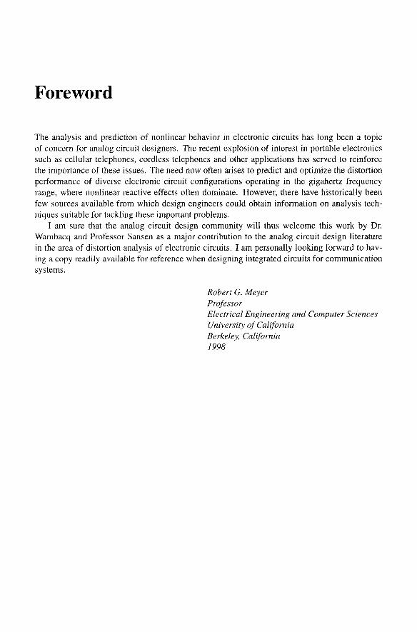
The analysis and prediction of nonlinear behavior in electronic circuits has long been a topic of concern for analog circuit designers. The recent explosion of interest in portable electronics such as cellular telephones, cordless telephones and other applications has served to reinforce the importance of these issues. The need now often arises to predict and optimize the distortion performance of diverse electronic circuit configurations operating in the gigahertz frequency range, where nonlinear reactive effects often dominate. However, there have historically been few sources available from which design engineers could obtain information on analysis techniques suitable for tackling these important problems.
I am sure that the analog circuit design community will thus welcome this work by Dr. Wambacq and Professor Sansen as a major contribution to the analog circuit design literature in the area of distortion analysis of electronic circuits. I am personally looking forward to having a copy readily available for reference when designing integrated circuits for communication systems.
Robert G. Meyer Professor Electrical Engineering and Computer Sciences University of California Berkeley, California 1998
Preface
In the world of electronics nowadays very advanced systems can be integrated on one chip. This is mainly possible by the ability to build complex functions with digital VLSI. However, not every functionality can be achieved using digital electronics. For example, some applications might require signal processing at a high frequency that is too high to process with digital circuitry. In that case, the signals must be processed with analog circuitry which can be integrated completely or partially.
Other applications require an interface between the digital electronics and the outside world, which behaves in an analog way. As a result, such interface functions are implemented with analog electronics, which again can be integrated.
The above considerations indicate that analog integrated circuits are required, not only as integrated circuits on their own, but also as part of large mixed-signal integrated circuits. In such mixed-signal systems more and more functions are implemented in a digital way. The specifications of the circuitry that remains to be designed in the analog domain are often very tough. As a result, circuit designers not only need to concentrate on the first-order characteristics of analog circuits, which can already be very complicated and which are most often attributed to the behavior of the linearized circuit. In addition, characteristics such as nonlinear behavior may become very critical.
In addition to mixed-signal applications that demand tough specifications for the analog blocks, there are some applications where the suppression of nonlinear behavior is of utmost importance. Examples are audio applications and telecommunication applications. In the latter applications, nonlinear behavior of the circuits induces intermodulation products, which together with the noise, increase the amount of "unwanted signals", thereby lowering the performance.
In the last few years, an increased interest is seen in the integration of analog high-frequency front-ends for telecommunication applications, both in CMOS and in BiCMOS. These technologies are quickly scaling to smaller dimensions, such that they can be used at ever increasing frequencies. In this way, these silicon technologies form a cheap alternative for GaAs. CMOS technologies are cheaper than BiCMOS technologies, but the bipolar (npn) transistors of the BiCMOS technologies are in general superior at high frequencies than the MOS transistors. Integrated silicon RF front ends are found in literature for wireless communications [Long 95], used for example in the GSM standard [Seven 91, Stet 95], the DECT standard [Daw 97], and the Japanese standard for the personal handy-phone system (PHS) [Sato 96], further in GPS (Global Positioning System) receivers [Herm 91], wireless local area networks (WLAN) [Madi 96, Har 96], in applications in the ISM bands (Industrial-Scientific-Medical) around 900MHz [Hull 96],
v
2.4GHz [Mey 97] or 5.7GHz [Voi 97], in the North American Digital Cellular (NADC) handset [Kara 96], and so on.
In analog RF front-ends for communication circuits, specifications that are related to nonlinear circuit behavior are very important. For example, if a receiver front-end is not very linear, then large incoming signals from the antenna will induce much extra distortion. Such large incoming signal may be a wanted signal but it can also be a strong unwanted signal at an adjacent frequency. The increased efforts of the analog design community in the silicon integration of analog high-frequency RF front-ends has been one of the motivations to write this book.
Not only the nonlinear behavior of the RF part of a communication circuit is important to control. In many communication circuits analog integrated filters are used, for example to perform the anti-aliasing filtering function right before an analog-digital converter in a receiver. The nonlinear distortion of these filters can degrade the overall performance of a transceiver. Veryoften 9m-C filters are used in transceivers [Gopi 90, Chang 97], since they can achieve high speeds. This high speed is achieved at the expense of a reduced nonlinearity. In essence, a 9m-C cell is an open-loop transconductor. We shall see in this book that the conversion of a voltage into a current, which is realized by a transconductor, is difficult to realize with a high linearity without an overall feedback with a large loop gain. Hence, nonlinear distortion is an important aspect in the design of an active analog integrated filter.
In many applications of analog circuits one is only interested in the circuits' steady-state behavior in response to a sinusoidal excitation or a combination of such excitations. Indeed, many circuit aspects are easier to characterize in the steady state. This is partially due to the fact that an extremely large class of analog circuits can be approximated very well by a linear system. Since sinusoidal functions are eigenfunctions of linear systems, the latter ones can be easily characterized in terms of responses to sinusoidal excitations. Examples of quantities that characterize a circuit in steady state are transfer characteristics like gain or impedances. These characteristics are also best measured when a circuit is in steady state. Gain and impedances are mainly due to the behavior of the linearized circuit. However, most analog integrated circuits behave weakly nonlinearly. This means that, when a sinusoidal signal or a combination of sinusoids is applied to a circuit, the output spectrum does not only contain signals with the same frequency of the input signals, as one would expect of a linear system: in addition, the output spectrum contains small components - usually unwanted - at frequencies other than the input signal frequencies. If one sinusoidal signal is applied at the input, then these unwanted signals occur at multiples of one of the input frequencies. In this case they are termed as harmonics. In the case of an excitation with more than one sinusoidal signal, unwanted components occur at frequencies which are linear combinations of the input frequencies. These components are denoted as intermodulation products.
The weakly nonlinear behavior of analog integrated circuits is caused by the slight curvature of the characteristics of the devices of the circuit around the operating point. This behavior contrasts with strongly nonlinear behavior, where devices such as transistors switch between an on-state and an off-state. Nonlinear behavior, both weakly and strongly nonlinear, are not always unwanted. For example, oscillators and mixers explicitly rely on nonlinearities for a suitable operation. This book is concentrated on weakly nonlinear behavior only. In this way, the majority of continuous-time analog integrated building blocks is covered.

vi
The harmonics or intermodulation products characterize the amount of nonlinearity of a given circuit. Since sinusoidal signals and sums of sinusoids are frequently used as inputs, a sinusoidal steady-state analysis of weakly nonlinear circuits is certainly not restrictive. Such analysis is carried out in the frequency domain.
The familiarity of circuit engineers with linear systems has given rise to many useful insights and design rules for circuits that can be approximated as linear. A circuit engineer is able to derive closed-form expressions for characteristics of a linearized circuit, which he can interpret and use afterwards during the synthesis of the circuit. If the circuit or its simplified schematic is too large to analyze with hand calculations, he can resort to a symbolic analyzer for linear(ized) circuits, but he still remains able to some extent to reason about the linear circuit's behavior even without explicitly having expressions for the characteristics.
On the other hand, the analysis and synthesis of circuits in which nonlinearities playa role, is difficult. Indeed, for such circuits just a few design rules exist in the analog design world. This has several reasons First, circuit designers are trained to reason only about linear systems, but not about nonlinear ones. Secondly, it is not easy to analyze nonlinear effects by hand calculations. The most studious designers use Taylor series, but this approach is only feasible in small circuits at low frequencies, with a very small number of nonlinearities. Usually, nonlinear effects are analyzed with tedious time-domain simulations (so-called transient simulations), followed by a Fourier analysis. Other approaches such as the harmonic balance techniques, although very useful, are not (yet) universally used. With both approaches the simulation results are numbers. These numbers can be plotted onto a graph, which can give valuable information, but they do not indicate the fundamental circuit parameters that determine the observed performance. As a result, circuit designers often do not know in which way a circuit can be improved in order to meet the specifications related to nonlinear behavior.
The above problem could be relieved if it were possible to indicate to circuit designers which circuit elements or which effects are mainly responsible for the observed nonlinear behavior. Such insight will be offered in this book for several building blocks of analog integrated circuits. In addition some general concepts of nonlinear behavior of analog integrated circuits will be studied as well.
This book is intended as a guide to learn designers of analog integrated circuits to reason about nonlinear phenomena in weakly nonlinear, continuous-time analog ICs. The required background to read this book is an understanding of analog integrated circuit design. A prior knowledge about theory of nonlinear systems, such as the theory of Volterra series, is not required. The background of Volterra series that is required to understand some essential concepts, is contained in this book.
When browsing through this book, the reader will notice the large number of formulas in this book. When one wants to reason about nonlinear phenomena, then a minimum amount of mathematics is required. It is virtually impossible to write a comprehensible text on nonlinear effects without mathematics. However, no special advanced mathematical techniques are used in this book. Also, the mathematics are explained as clearly as possible, they are interpreted and illustrated with examples, and tedious derivatives are moved to appendices at the end of the book.
This book is devoted to the analysis in the frequency domain of weakly nonlinear circuits. The circuits that are addressed are building blocks of analog integrated circuits, both in bipolar
vii
and CMOS technologies. The emphasis is on getting insight, both in the nonlinearities in the transistors themselves, as in the nonlinear behavior of transistor circuits.
The outline of the text is as follows:
- Chapter 1 pr,,?sents an overview of the approach that is followed in this book. Further, some assumptions are made about the nonlinear circuits that will be analyzed in this book, and the scope of the book will be outlined.
- In the analog design community, many definitions and keywords are used to characterize the nonlinear behavior of analog circuits in the frequency domain. This basic terminology is described in Chapter 2.
- In order to analyze the nonlinear behavior of a circuit, we need to describe the different nonlinearities in the circuit under consideration with a sufficient accuracy. To this purpose, we will make use of power series expansions of the model equations that describe a nonlinear device. It will turn out that a device such as a transistor consists of several basic nonlinear elements, such as nonlinear conductances, transconductances and capacitors. Each of these elements can be described with a power series. The coefficients of these power series are proportional to the derivatives of the model equations that describe these basic nonlinear elements. These power series coefficients, further in the text referred to as nonlinearity coefficients determine the nonlinear behavior behavior of a circuit. In Chapter 3, these power series are presented together with some simple examples.
- A very useful technique to describe the nonlinear behavior of weakly nonlinear circuits is the Volterra series approach, which is covered in Chapter 4. With Volterra series, it is possible to take into account frequency effects into the calculations of harmonics and intermodulation products. This is absolutely necessary if one wants to study circuits with capacitors, both linear and nonlinear. Further, we will use Volterra series to study some general concepts in nonlinear circuits: the use of feedback, both linear and nonlinear, the exploitation of symmetry for the suppression of even-order or odd-order harmonics, the effect of cascading nonlinear circuits, and pre- and post-distortion will be studied.
- Calculation methods for harmonics and intermodulation products are discussed in Chapter 5. The emphasis is on. methods that allow to generate closed-form expressions for harmonics or intermodulation products. Numerical methods will be discussed briefly.
For the generation of closed-form expressions a calculation method can be used that makes use of Volterra series. This method is explained with an example. Derivations can be found in literature [Buss 74, Chua 79b]. Further, an alternative method is developed in this chapter that yields the same results without making use of Volterra series.
With both methods the circuit is analyzed in the frequency domain. In fact, we perform an AC analysis on a circuit in which the nonlinear elements are not only represented by their linearized equivalent: in addition, the second- and third-order nonlinear behavior are taken into account as well.

viii
Despite the availability of different methods to obtain closed-form expressions for harmonics or intermodulation products, the use of these methods for hand calculations is too tedious, even for very small circuits. With a symbolic network analysis program, however, it is possible to automate these hand calculations and to obtain a closed-form expression. Symbolic network analysis programs can compute a closed-form expression for the AC behavior of a linearized circuit as a function of the symbolic small-signal parameters of the circuit and of the complex frequency variable. Modern symbolic analysis programs, such as the program ISAAC [Giel 89, Giel 91], can even generate approximate symbolic expressions. The approximation is made because the exact expression is usually too lengthy, such that it cannot be easily interpreted. An approximation based upon numerical values for the circuit parameters can retain the few dominant terms of an expression, such that the resulting expression becomes interpretable. In Chapter 5 an extension of the program ISAAC is described for the generation of approximate, interpretable expressions for nonlinear distortion.
- The nonlinearity coefficients of the different nonlinearities in a bipolar transistor and a MOS transistor are discussed in Chapters 6 and 7, respectively. Whereas for the bipolar transistor the Gummel-Poon model is still widely used or it forms the basis of more recent models [Mc And 95], the situation for a MOS transistor is more complicated. Due to the rapid scaling of a MOS transistor, effects that were recognized as second-order effects in older technologies, become dominant in modern devices. If these effects are not included in a transistor model or if they are badly modeled, then this may lead to very large errors on the harmonics or intermodulation products. The reason is that the nonlinearity coefficients are proportional to higher-order derivatives. The error on these derivatives tends to increase dramatically when the model equation is inaccurate. In Chapter 7 some shortcomings of widely used transistor models will be discussed. Further, a model for the drain current will be presented that will be used to derive closed-form expressions for the nonlinearity coefficients.
- Apart from the examples that have been used throughout the individual chapters, some more applications are described in Chapter 8. Distortion wiII be analyzed for the following circuits: a single-transistor amplifier, both a bipolar and a MOS version, a bipolar and a MOS differential pair, a source follower, an emitter follower, a bipolar transistor with emitter degeneration, a common-base bipolar and a common-gate MOS transistor, a bipolar and a MOS current mirror, a Miller-compensated operational amplifier, a bipolar double-balanced mixer, and a CMOS upconverter. Hereby, use will be made of the extension of the program ISAAC to generate closed-form expressions for distortion.
- Instead of computing the nonlinearity coefficients, it is also possible to measure these coefficients. A measurement procedure and measurement results on bipolar transistors are given in Chapter 9.
Finally the authors would like to thank the following persons for their discussions and comments: Peter Kinget from Lucent Technologies, Murray Hill, Yannis Tsividis from the University of Columbia, New York, Stephane Donnay, Hugo De Man and Luc Dupas from IMEC,
ix
Leuven, Georges Gielen, Walter Daems and Joos Vandewalle from the ESAT Laboratories of the Catholic University of Leuven, Petr Dobrovolny from the University of Brno, Czech Republic, Guang-Ming Yin and Frederic Stubbe from Rockwell Semiconductor Systems, Newport Beach, California, Frank Op 't Eynde from AIcatel Microelectronics, Brussels, Paco Fernandez from IMSE-CNM. Seville, Spain, Jan Vanthienen, and, last but not least, Kaat Fran<;ois for her support and patience.
Piet Wambacq Willy Sansen

x
TO OUR FAMILIES Kaat, Lien, and Elli
Hadewych, Katrien, Sara, and Marjan
xi
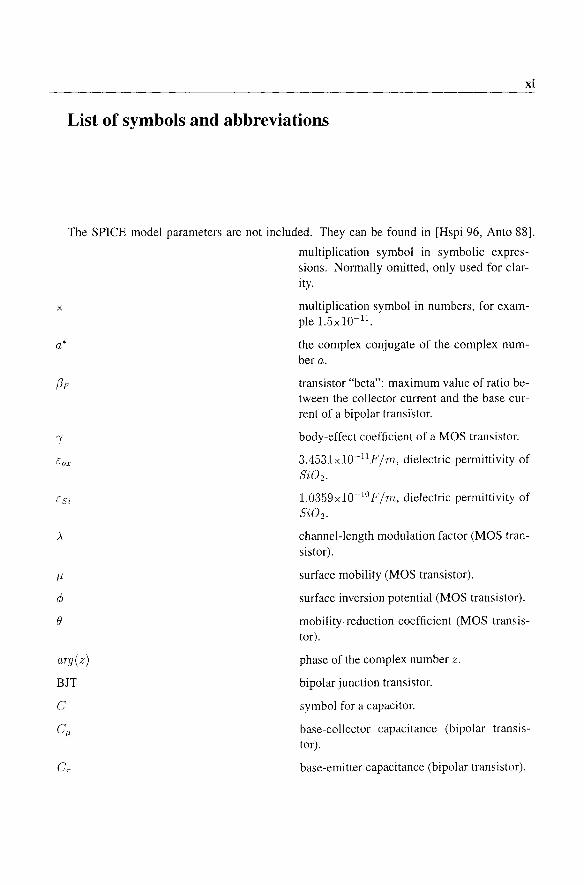
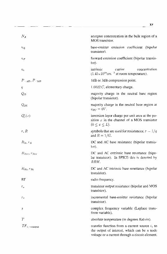
List of symbols and abbreviations
The SPICE model parameters are not included. They can be found in [Hspi 96, Anto 88].
multiplication symbol in symbolic expressions. Normally omitted, only used for clarity.
x
a*
i3F
Cox
arg(z)
BJT
C
Cf.L
C1r
multiplication symbol in numbers, for example 1.5x10⁻¹¹ •
the complex conjugate of the complex number a.
transistor "beta": maximum value of ratio between the collector current and the base current of a bipolar transistor.
body-effect coefficient of a MOS transistor.
3.4531 x 10- 11 F 1m, dielectric permittivity of Si0 2 .
1.0359x 10⁻¹⁰ F 1m, dielectric permittivity of Si0 2 .
channel-length modulation factor (MOS transistor).
surface mobility (MOS transistor).
surface inversion potential (MOS transistor).
mobility-reduction coefficient (MOS transistor).
phase of the complex number z.
bipolar junction transistor.
symbol for a capacitor.
base-collector capacitance (bipolar transistor).
base-emitter capacitance (bipolar transistor).
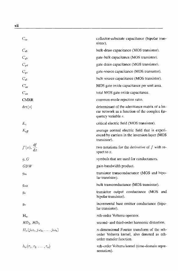
xii
Ccs
C db
C gb
C gd
C gs
C sb
C~x
Cox
CMRR
det(s)
f'(x), :~
g,G
GBW
gm
gmb
go
g",
collector-substrate capacitance (bipolar transistor).
bulk-drain capacitance (MOS transistor).
gate-bulk capacitance (MOS transistor).
gate-drain capacitance (MOS transistor).
gate-source capacitance (MOS transistor).
bulk-source capacitance (MOS transistor).
MOS gate oxide capacitance per unit area.
total MOS gate oxide capacitance.
common-mode rejection ratio.
determinant of the admittance matrix of a linear network as a function of the complex fJ;equency variable s.
critical electric field (MOS transistor).
average normal electric field that is experienced by carriers in the inversion layer (MOS transistor).
two notations for the derivative of f with respect to x.
symbols that are used for conductances.
gain-bandwidth product.
transistor transconductance (MOS and bipolar transistor).
bulk transconductance (MOS transistor).
transistor output conductance (MOS and bipolar transistor).
incremental base-emitter conductance (bipolar transistor).
nth-order Volterra operator.
second- and third-order harmonic distortion.
n-dimensional Fourier transform of the nthorder Volterra kernel, also denoted as nthorder transfer function.
nth-order Volterra kernel (time-domain representation).
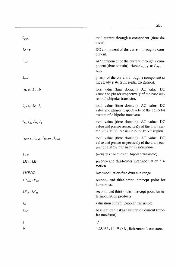
iOUT
lOUT
lout
IMFDR
Is
isE
j
k
xiii
total current through a component (time domain).
DC component of the current through a component.
AC component of the current through a component (time domain). Hence iOUT = I ouT+ i out .
phasor of the current through a component in the steady state (sinusoidal excitation).
total value (time domain), AC value, DC value and phasor respectively of the base current of a bipolar transistor.
total value (time domain), AC value, DC value and phasor respectively of the collector current of a bipolar transistor.
total value (time domain), AC value, DC value and phasor respectively of the drain current of a MOS transistor in the triode region.
total value (time domain), AC value, DC value and phasor respectively of the drain current of a MOS transistor in saturation.
forward knee current (bipolar transistor).
second- and third-order interrnodulation distortion.
interrnodulation-free dynamic range.
second- and third-order intercept point for harmonics.
second- and third-order intercept point for intermodulation products.
saturation current (bipolar transistor).
base-emitter leakage saturation current (bipolar transistor).
1.38062x 10⁻²³ J / K, Boltzmann's constant.
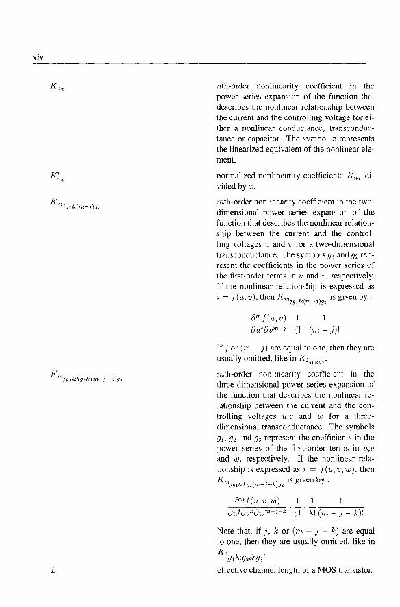
xiv
K' nx
L
nth-order nonlinearity coefficient in the power series expansion of the function that describes the nonlinear relationship between the current and the controlling voltage for either a nonlinear conductance, transconductance or capacitor. The symbol x represents the linearized equivalent of the nonlinear element.
normalized nonlinearity coefficient: Knx divided by x.
mth-order nonlinearity coefficient in the twodimensional power series expansion of the function that describes the nonlinear relationship between the current and the controlling voltages u and v for a two-dimensional transconductance. The symbols gl and g2 represent the coefficients in the power series of the first-order terms in u and v, respectively. If the nonlinear relationship is expressed as i = f(u, v), then Km &( 0) is given by:
)91 m-) 92
8m f(u, v) 1 1 8uj8vm- j j! (m - j)!
If j or (m - j) are equal to one, then they are usually omitted, like in K 291 &92 •
mth-order nonlinearity coefficient in the three-dimensional power series expansion of the function that describes the nonlinear relationship between the current and the controlling voltages u,v and w for a threedimensional transconductance. The symbols gl, g2 and g3 represent the coefficients in the power series of the first-order terms in u,v and w, respectively. If the nonlinear relationship is expressed as i = f (u, v, w), then Km &k ( 0 k) is given by :
)91 92 m-)- 93
[}fflf(u,v,w) 1 1 1 8uj8vk8wm-j-k . J! . k! (m - j - k)!
Note that, if j, k or (m - j - k) are equal to one, then they are usually omitted, like in
K3 & & . gl g2 g3
effective channel length of a MOS transistor.
q
QB
QBO
Q~(x)
r,R
RF
s
T
TFi,-+Output
xv
acceptor concentration in the bulk region of a MOS transistor.
base-emitter emission coefficient (bipolar transistor) .
forward emission coefficient (bipolar transistor).
intrinsic carrier concentration (1.45x 1010cm-3 at room temperature).
IdB or 3dB compression point.
1.6022 C, elementary charge.
majority charge in the neutral base region (bipolar transistor).
majority charge in the neutral base region at VBe = OV.
inversion layer charge per unit area at the position x in the channel of a MOS transistor (O:<::;x:<::;L).
symbols that are used for resistances; r = 1/ g
andR = l/C.
DC and AC base resistance (bipolar transistor).
DC and AC extrinsic base resistance (bipolar transistor). In SPICE this is denoted by REM.
DC and AC intrinsic base resistance (bipolar transistor) .
radio frequency.
transistor output resistance (bipolar and MOS transistor).
incremental base-emitter resistance (bipolar transistor).
complex frequency variable (Laplace transform variable).
absolute temperature (in degrees Kelvin).
transfer function from a current source i 1 to the output of interest, which can be a node voltage or a current through a circuit element.
xvi
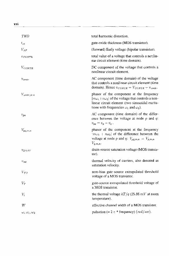
THD total harmonic distortion.
tax gate-oxide thickness (MOS transistor).
V AF (forward) Early voltage (bipolar transistor).
VCONTR total value of a voltage that controls a no:.lin-ear circuit element (time domain).
VCONTR DC component of the voltage that controls a nonlinear circuit element.
Vcontr AC component (time domain) of the voltage that controls a nonlinear circuit element (time domain). Hence VCONTR = VCONTR + Vcantr·
Vcontr,m.n phasor of the component at the frequency Imwi +nw21 of the voltage that controls a non-linear circuit element (two sinusoidal excita-tions with frequencies WI and W2).
Vpq AC component (time domain) of the differ-ence between the voltage at node p and q: Vpq = vp - Vq .
Ypq,m,n phasor of the component at the frequency Imwi + nW21 of the difference between the voltage at node p and q: Ypq,m,n = Vp,m,n -
Vq,m,n.
VDSAT drain-source saturation voltage (MOS transis-tor).
Vsat thermal velocity of carriers, also denoted as saturation velocity.
V TO zero-bias gate-source extrapolated threshold voltage of a MOS transistor.
V T gate-source extrapolated threshold voltage of a MOS transistor.
VI the thermal voltage kT j q (25.86 m V at room temperature).
W effective channel width of a MOS transistor.
w, WI, W2 pulsation (= 2 7r * frequency) (radj sec).
Contents
Foreword
Preface
List of symbols and abbreviations
Contents
1 Introduction 1.1 Scope of this book
2 Basic terminology 2.1 Introduction. 2.2 Single-frequency excitation. . . . . . .. 2.3 Even-order and odd-order distortion only 2.4 Two-frequency excitation . 2.5 Mixer definitions 2.6 Cross modulation 2.7 Summary . . . .
3 Description of nonlinearities in analog integrated circuits 3.1 Introduction ..................... .
iii
iv
xi
xvii
1 4
7 7 7
16 17 23 24 25
26 26
3.2 Power series description of basic nonlinearities .... 29 3.2.1 Nonlinear conductance and transconductance . 31
3.2.1.1 Example: collector current of a BJT 32 3.2.1.2 Example: base current of a BJT . . . 33
3.2.2 Nonlinear resistance . . . . . . . . . . . . . . 34 3.2.2.1 Conversion formulas between a voltage-controlled description
and a current-controlled description. . . . 35 3.2.2.2 Difference between DC and AC resistance 37
3.2.3 Nonlinear capacitance . . . . . . . . . . 38 3.2.3.1 Example: diffusion capacitance 39
3.2.4 Two-dimensional transconductance .. . 39
xviii
3.2.4.1 Example: two-dimensional collector current 3.2.5 Three-dimensional transconductance ......... .
3.2.5.1 Example: drain current of a MOS transistor 3.2.6 Tracking nonlinearities ................ .
3.3 Integrated resistors ...................... . 3.3.1 Nonlinearity coefficients of an implanted or diffused resistor
3.3.1.1 Example ........... . 3.4 Integrated capacitors . . . . . . . . . . . . . . . 3.5 Weakly nonlinear transistor models: introduction 3.6 Summary .................... .
4 Volterra series and their applications to analog integrated circuit design 4.1 Introduction........ 4.2 Basics of Volterra series. . . . . . .
4.2.1 Volterra operators . . . . . . 4.2.2 Time-domain fundamentals 4.2.3 Frequency-domain representation 4.2.4 Weakly nonlinear circuit behavior revisited
4.3 Examples of Volterra kernels . . . 4.3.1 Basic second-order system ... . 4.3.2 Basic third-order system .... . 4.3.3 Application: a nonlinear amplifier
4.4 Nonlinear performance parameters in terms of Volterra kernels 4.4.1 Single-tone and two-tone definitions . . 4.4.2 Cross modulation . . . . . . . . . . . . . . .
4.5 Suppression of even-order or odd-order kernels ... 4.5.1 Application: suppression in a differential pair 4.5.2 Application: suppression in a Gilbert multiplier.
4.6 Cascade connection of nonlinear systems 4.6.1 General expressions ............. . 4.6.2 Application: a two-stage amplifier . . . . . . .
4.7 Pre-distortion and post-distortion using inverse systems 4.7.1 General expressions 4.7.2 Example ...... . 4.7.3 Applications .... .
4.8 Linear and nonlinear feedback 4.8.1 Nonlinear feedback systems 4.8.2 Feedback with a large loop gain 4.8.3 Linear feedback. . . . . . . . .
4.8.3.1 Simplification to memoryless systems 4.8.3.2 Application: emitter degeneration . .
4.8.4 Nonlinearities in the feedback network .... 4.8.5 Loading effect of a nonlinear feedback network
CONTENTS
40 41 42 45 47 48 51 52 55 57
S9 59 61 62 63 65 67 68 68 69 71 75 75 79 80 81 84 85 86 88 88 89 89 91 93 94 96 97 98
100 103 103

CONTENTS
4.8.6 Operational amplifier in a linear feedback configuration 4.8.7 Nonlinear feedback applications
4.9 Summary . . . . . . . . . . . . . . . . . . . . . . .
5 Calculation of harmonics and intermodulation products 5.1 Introduction ......... . 5.2 Calculation of Volterra kernels
5.2.1 First-order kernels . 5.2.2 Second-order kernels . 5.2.3 Third-order kernels .. 5.2.4 5.2.5 5.2.6 5.2.7 5.2.8
Postprocessing of the results Simplifications . . . . . . . Volterra kernels of currents . Interpretation of the results . Factorization of the denominators
xix
lOS 113 114
116 116 119 120 122 126 128 131 132 133 134
5.3 Direct calculation of nonlinear responses. 137 5.3.1 First-order responses . . . . . . . 139 5.3.2 Second-order responses ..... 143 5.3.3 Third-order and higher-order responses 147 5.3.4 Interpretation and factorization. . . . . ISS
5.4 Symbolic computation of harmonics and intermodulation products 156 5.4.1 Symbolic network analysis of linearized analog circuits. . 158 5.4.2 Symbolic analysis of weakly nonlinear analog circuits with ISAAC 162
5.4.2.1 Elimination of unimportant nonlinearities. . . . . . . . . 163 5.4.2.2 Generation of the approximate symbolic subexpressions . 164
5.5 Simple example circuits. . . . . . . . . . . 164 5.5.1 Nonlinear resistive voltage divider. 164 5.5.2 Nonlinear capacitive current divider 171
5.6 Numerical verification with other methods 175 5.6.1 Numerical integration .. . 5.6.2 Shooting methods ..... . 5.6.3 Harmonic balance methods .. 5.6.4 Example: an emitter follower
5.7 Summary .............. .
6 Silicon bipolar transistor models for distortion analysis 6.1 Introduction..................... 6.2 The collector current . . . . . . . . . . . . . . . .
6.2.1 Collector current with a linear Early effect. 6.2.2 Nonlinearity of the Early effect
6.3 The base current. . . . . . . . . . . . . . . 6.4 The base resistance . . . . . . . . . . . . .
6.4.1 Modeling of the current dependence
175 176 176 177 178
180 180 182 182 184 188 190 192
xx
6.4.2 DC and AC base resistance and the nonlinearity coefficients 6.4.3 Evaluation of the nonlinearity coefficients
6.5 Capacitors in a bipolar transistor 6.6 Summary . . . . . . . . . . . . . . . . . .
CONTENTS
193 195 196 199
7 MOS transistor models for distortion analysis 200 .200 7.1 Introduction ................ .
7.2 Nonlinearity coefficients of the three-dimensional drain current nonlinearity . 203 7.2.1 Coefficients referred to the source . . . . . . . . . . . . . . . . .. . 206 7.2.2 Coefficients referred to the bulk . . . . . . . . . . . . . . . . . .. . 206 7.2.3 Relationship between the coefficients of the two reference systems. . 208
7.3 Basic relations for the drain current in strong inversion . . . . . . 210 7.4 Drain current in the triode region without small-geometry effects . 212
7.4.1 Uniform depletion layer . . . . . . . . . . . . . . . . . . 212 7.4.1.1 Application: a single-transistor mixer. . . . . . 216 7.4.1.2 Formulation of the current in terms of VCB, VDB and VSB . 217
7.4.2 Nonuniform depletion layer . . . . . . . . . . . 217 7.4.3 Simplification: linearly varying depletion layer . . . 221 7.4.4 Comparison of nonlinearity coefficients . . . . . . . 223
7.5 Drain current in saturation without small-geometry effects . 225 7.5.1 Uniform depletion layer . . . . . . . . . . . . . 226 7.5.2 Nonuniform depletion layer . . . . . . . . . . . 228 7.5.3 Simplification: linearly varying depletion layer . 229 7.5.4 Comparison of nonlinearity coefficients . 229
7.6 Effective mobility . . . . . . . . . . . . . . . . . 231 7.6.1 Mobility model of Sabnis and Clemens . 231 7.6.2 Drain current in the triode region. . . . 232 7.6.3 Drain current in the saturation region . . 235 7.6.4 Other mobility models . . . . . . . . . . 236
7.6.4.1 The mobility model of Frohman-Bentchkowsky . 236 7.6.4.2 The mobility model of Liang et al. . 237
7.6.5 Evaluation of nonlinearity coefficients . 238 7.6.5.1 Triode region .. . 238 7.6.5.2 Saturation region . 245
7.7 Velocity saturation ......... . 245 7.7.1 Velocity-field models. . . . . 247 7.7.2 Drain current in the triode region. . 248
7.7.2.1 Drain current with the simple velocity-field models . 249 7.7.2.2 The functions large, mobred and hot . . . . . . . . . 249 7.7.2.3 Merging of the functions mobred and hot . 250 7.7.2.4 Drain current with the more accurate velocity-field model . 251 7.7.2.5 Modelling around VDS = OV . 252
7.7.3 Drain current in the saturation region ................ . 253
CONTENTS xxi
7.7.3.1 Drain current in saturation with the simple velocity-field models 253 7.7.3.2 Merging of the functions mobred and hot ........... 255 7.7.3.3 Drain current in saturation with the more accurate velocity-
field model . . . . . . . . . . . . . . . . . . . . 256 7.7.4 Evaluation of nonlinearity coefficients ................... 257
7.7.4.1 Nonlinearity coefficients for the triode region ......... 258 7.7.4.2 Approximate expressions for the nonlinearity coefficients in
the triode region . . . . . . . . . . . . . . . . . . . . . . . . . 258 7.7.4.3 Nonlinearity coefficients for the saturation region ....... 267 7.7.4.4 Approximate expressions for the nonlinearity coefficients in
the saturation region . . . . . . . . . . . 268 7.8 Nonuniform doping effects . . . . . . . . . . . . . . . . . 273
7.8.1 Modeling with one single body-effect coefficient . 276 7.8.2 Adaption of the threshold voltage expression . 276 7.8.3 Drain current model with three equations . . . . . 277 7.8.4 Mobility reduction . . . . . . . . . . . . . . . . . 277
7.9 Threshold voltage for short- and narrow-channel devices . 278 7.10 Source and drain resistances ............... . 280
7.10.1 Source and drain resistance components in conventional devices . 281 7.10.2 LDD structures . . . . . . . . . . . . . . . . . . . . . . . . . . 281 7.10.3 Effect on the drain current and on the nonlinearity coefficients . 282
7.11 The output conductance and its derivatives in saturation . . . . 283 7.11.1 The physical model of Huang et al. ........... . 284
7.11.1.1 Contribution of channel-length modulation . . . 286 7.11.1.2 Contribution of drain-induced barrier lowering . 287 7.11.1.3 Contribution of the substrate current . . . . . . 288 7.11.1.4 Continuity of the output conductance . . . . . . 289 7.11.1.5 Evaluation of the output conductance and its derivatives . 289 7.11.1.6 Evaluation of other nonlinearity coefficients in saturation . 292
7.12 Capacitors in a MOS transistor . 292 7.12.1 Extrinsic capacitors . . . . . . . . . 293 7.12.2 Intrinsic capacitors . . . . . . . . . 294
7.13 Drain current in weak inversion operation . 297 7.13.1 Expression of the drain current . . . 297 7.13.2 Nonlinearity coefficients of the drain current in weak inversion. . 298
7.14 Summary . . . . . . . . . . . . . . . . . . . . . . . . . . . . . . . . . . 300
8 Weakly nonlinear behavior of basic analog building blocks 302 8.1 Introduction............. . 302 8.2 Single bipolar transistor amplifier ............ . 303
8.2.1 Elementary transistor model . . . . . . . . . . . . 304 8.2.1.1 Computation of harmonics from the DC transfer characteristic 304 8.2.1.2 Computation of harmonics with the method of Section 5.3 ... 307
xxii
8.2.2 Influence of the output resistance 8.2.2.1 Fundamental response . 8.2.2.2 Second harmonic .. . 8.2.2.3 Third harmonic ... .
8.2.3 Influence of the source resistance 8.2.3.1 Fundamental response. 8.2.3.2 Second harmonic .. 8.2.3.3 Third harmonic ....
8.2.4 Influence of the base resistance .. 8.2.4.1 Fundamental response . 8.2.4.2 Second harmonic 8.2.4.3 Third harmonic
8.2.5 Influence of C" . . . . . 8.2.5.1 Current drive. 8.2.5.2 Voltage drive.
8.2.6 Influence of CM and Ccs 8.2.6.1 Fundamental response . 8.2.6.2 Second harmonic distortion 8.2.6.3 Third harmonic distortion .
CONTENTS
.310 · 310 · 311 · 314 · 315 · 315 · 315 · 318 · 319 .320 .320 · 323 · 325 .325 · 327 · 333 · 333 · 337 · 343
8.2.6.4 Third harmonic distortion with different values of CM • 347 8.3 Single MOS transistor amplifier . . . . . . . . . . . . 350
8.3.1 Influence of gm only . . . . . . . . . . . . . . 350 8.3.1.1 Transistor in the saturation region . . 352 8.3.1.2 Transistor in the triode region . . . . 354 8.3.1.3 Transistor in the weak inversion region . 354
8.3.2 Influence of the output conductance . 355 8.3.3 Frequency behavior. . . . . . . . . . . 357
8.3.3.1 First-order response . . . . . 358 8.3.3.2 Second harmonic distortion . 360 8.3.3.3 Third harmonic distortion . . 365
8.4 Bipolar differential pair. . . . . . . . . . . . . 366 8.4.1 Computation of harmonics from the DC transfer characteristic . 367 8.4.2 Symbolic analysis of HD3 . 369 8.4.3 HD2 due to mismatches . . . . . . . . . . . . . . . . . . . . . 372
8.5 MOS differential pair . . . . . . . . . . . . . . . . . . . . . . . . . . . 375 8.5.1 Computation of harmonics from the DC transfer characteristic . 376 8.5.2 Computation of HD3 including the bulk effect . 378 8.5.3 HD2 due to mismatches . 384
8.6 Emitter follower. . . . . . . . . 386 8.6.1 First-order response . . 387 8.6.2 Second-order response . 388 8.6.3 Third-order response . 390
8.7 Source follower . . . . . . . . . 391
CONTENTS
8.7.1 First-order response . 8.7.2 Second-order response 8.7.3 Third-order response
8.8 Cascode transistor. . . . . . . 8.8.1 Bipolar cascode. . . .
8.8.1.1 First-order response 8.8.1.2 Second-order response. 8.8.1.3 Third-order response .
8.8.2 MOS cascode . . . . . . . . . . . 8.9 Common-gate and common-base transistor
8.9.1 First-order response . 8.9.2 Second-order response 8.9.3 Third-order response .
8.10 Current mirrors . . . . . . . . 8.10.1 DC transfer characteristic for a bipolar current mirror. 8.10.2 Distortion in a MOS current mirror
8.10.2.1 First-order response .. 8.10.2.2 Second-order response. 8.10.2.3 Third-order response . 8.10.2.4 Numerical example ..
8.10.3 Distortion in a bipolar current mirror. 8.11 Bipolar double-balanced mixer . . . . . . . . 8.12 CMOS Miller-compensated operational amplifier 8.13 CMOS upconverter 8.14 Summary . . . . . . . . . . . . . . . . . . . . .
9 Measurements of basic nonlinearities of transistors 9.1 Introduction ......... . 9.2 Principle of the measurements 9.3 Practical applications .... . 9.4 Measurement results .... .
9.4.1 Derivatives of ic with respect to VEE
9.4.2 The nonlinearity of the Early resistance 9.4.3 Cross-derivatives of ic
9.5 Summary .......... .
Bibliography
Appendices
A Useful trigonometric relationships
xxiii
· 392 .392
· 395 · 397 · 397 · 398 · 399 .401 .401 .401 .403 .404 .406 .407 .407 .409 .410 .410 .412 .412 .413 .414 .417 .420 .427
429 .429 .430 · 431 .433 .434 .436 · 438 .439
440
456
456
xxiv
B Basics of Volterra series B.! Introduction .... B.2 Volterra series representation of a system. B.3 Second-order Volterra systems . . . . . .
B.3.! The second-order operator .... B.3.2 The second-order Volterra operator B.3.3 Second-order kernel symmetrization.
B.4 The second-order kernel transform . . . . . . BA. ! The two-dimensional Fourier and Laplace transform BA.2 Sinusoidal response of a second-order Volterra system BA.3 Response of a second-order system to a sum of two sinusoids
B.5 Higher-order Volterra systems .... . B.5.! The pth-order operator .... . B.5.2 The pth-order Volterra operator B.5.3 pth-order kernel symmetrization B.5A The p-dimensional Laplace and Fourier transforms
CONTENTS
458 .458 .458 .459 .460 .460 .463 .463 .463 .464 .466 .466 .466 .467 .468 .468
C Derivation of the method for the direct computation of nonlinear responses 470 C.! Setup of basic equations . 470 C.2 First-order responses . . 473 C.3 Second-order responses . 474 CA Higher-order responses . 477
D Nonlinearity coefficients for the description of the Early effect 478
E Relation between source-referred and bulk-referred nonlinearity coefficients of a MOS transistor 482
F Derivatives of the drain current with an implicit saturation voltage 486 F! Determination of VnSAT . 487 F2 First-order derivatives. . . 487 F3 Higher-order derivatives . 488
G Derivation of the MOS drain current in the presence of velocity saturation 490 G.! Derivation of the drain current with the simple velocity-field models . . . . 491 G.2 Derivation of the drain current with the more accurate velocity-field model. . 492
G.2.! The rigorous approach . 492 G.2.2 Approximate approach . . . . . . . . . . . . . . . . . . . . . . .. . 493
Index 495


