Page 1
DISTORTION MEASUREMENT IN AUDIO AMPLIFIERS.
By Michael Renardson.
SUMMARY
The requirements for the measurement of non-linear distortion
in audio power amplifiers are examined. The limitations of
conventional measurement methods are discussed and several
improved test methods described in which complex test signals
could be used. A detailed examination is made of one method in
which the input and output signals of an amplifier are
combined in such a way that the undistorted component of the
output signal is cancelled by the input signal and the
distortion component isolated. The existing literature
concerning this method is surveyed. The sources of error when
using this technique are examined. These include phase and
gain errors at high and low frequencies, earth connection
arrangements and the effects of complex loads. Methods of
reducing the errors are explained and a practical measuring
instrument circuit designed.
The instrument has a differential input so that inverting,
non-inverting or differential amplifiers can be tested and
uses a simple adjustable second order high frequency phase
and gain compensation network. The distortion and noise of
the instrument are analysed. The practical performance of
the instrument is evaluated and its distortion contribution
shown to be of an extremely low value. The rejection of test
signal distortion is calculated for a particular amplifier
test and shown to be more than adequate even when measuring
extremely low harmonic distortion. The effectiveness of the
load effect compensation arrangement derived is
demonstrated. Finally some of the uses of the instrument are
illustrated in tests on a typical class-B power amplifier to
detect crossover distortion, transient intermodulation
distortion and phase modulation.
Page 2
CHAPTER 1
DISTORTION MEASUREMENT TECHNIQUES.
1.1 Requirements for the measurement of distortion in audio
frequency power amplifiers.
In an ideal audio frequency power amplifier the output signal
voltage would be identical to the input signal voltage
multiplied by a constant. The input impedance would be
infinite so that there would be no loading effect on the
signal source, and the output impedance would be zero so that
the output voltage would be independent of the load used. In
the design of a practical amplifier it is necessary to decide
to what extent the requirements can be reduced and to be able
to measure the deviation from the ideal when using input
signals having similar characteristics to those for which the
amplifier is designed. Some types of distortion are more
audible than others and a test method is required in which
the resulting distortion specification gives a good
indication of how the amplifier will sound in practical use.
The input and output impedance requirements depend on the
signal source impedance, Zs, and load impedance, Zl,
respectively. For a given degree of non-linearity in the
input impedance the distortion introduced will be minimised
by the use of a low value of Zs, so distortion should be
measured using the largest value of Zs to be used in the
intended application of the amplifier to give a worst case
figure. Comparison of the results with those obtained using a
much lower value of Zs will indicate the relative
significance of this source of distortion.
For a given degree of non-linearity in the output impedance
the resulting distortion will be dependent on the load used.
Although many loudspeakers are specified as having an
impedance of 8 ohms there is usually a large variation
throughout the audio frequency range with typical variations
Page 3
in a given loudspeaker from 5 to 40 ohms (Ref.1,2) and
significant reactive components. The distortion produced by
an amplifier with a loudspeaker load will therefore be
different from that with an 8 ohm resistor and the total
harmonic distortion figure is typically 10 dB higher over
much of the frequency range (Ref.3) and in some cases
considerably worse. (Ref.4) If possible distortion
measurements should therefore be carried out using various
typical loudspeaker loads to give an indication of the
performance under normal operating conditions. Comparison
with measurements made with no load connected will give an
indication of the relative significance of distortion due to
non-linearity in the output impedance. It should be noted
however that in class-B amplifiers crossover distortion can
occur at low output currents and may sometimes be more
significant when using high load impedances if operation is
then confined to the non-linear crossover region.
A distortion component would still be present even with a
zero source impedance and no load. There are therefore three
separate components of distortion to be considered, and for a
general purpose amplifier in which different source and load
impedances may be used it would be an advantage to obtain
measurements of the three components separately, or at least
to present the total distortion figure as a function of
source and load impedances.
1.2 Distortion specifications and measurement methods.
It is convenient to specify the distortion of an amplifier in
a form which enables comparison with other amplifiers or with
some known standard requirement, e.g. the DIN 45 500 (Ref.5)
standard for audio power amplifiers specifies a maximum
r.m.s. total harmonic distortion of 1 % for sine wave signals
from 40 Hz to 12.5 kHz for any power output between 100 mW
and 10 W and intermodulation distortion no more than 3 % at
10 W output for inputs of 250 Hz and 8 kHz with an amplitude
Page 4
ratio of 4:1. Other minimum standards for high quality sound
reproduction (Ref.6,7,8) have been proposed which demand much
lower levels of distortion, although there is some
disagreement about the audibility of various quantities and
types of distortion in amplifiers when used for the
reproduction of music. (Ref.8 to 13).
Total harmonic distortion (t.h.d.) measurements can be made
using a distortion factor meter, which is basically a
variable frequency notch filter. A low distortion sine wave
is applied to the input of the amplifier being tested and the
output fed to the input of the notch filter, which is
adjusted to eliminate the frequency of the test signal. The
remaining signal contains distortion and noise from the
amplifier and can be measured on a r.m.s. meter to give a
percentage t.h.d. This signal will contain components over a
wide frequency range and as the r.m.s. value will depend on
the bandwidth of the measuring system a bandpass filter is
generally incorporated in the instrument. The bandwidth used
must be stated as part of the distortion specification.
The limitations of this technique are:
1). The inability of the instrument to distinguish between
the distortion added by the amplifier and that already
present in the test signal or added by the input stages of
the instrument itself. A signal generator with very low
distortion must be used
2). The inclusion of amplifier noise over the wide bandwidth
which may be needed to include all significant distortion
components. In extreme cases the "t.h.d." measured may be
predominantly noise. The standard method of t.h.d.
specification makes no allowance for this possibility
(Ref.14) and can therefore be misleading.
3). For frequencies above 10 kHz the harmonics will all be
outside the audible frequency range and therefore knowledge
of their amplitudes can only give an indirect indication of
the importance of high frequency non-linearity. When
Page 5
reproducing complex audio signals any audible distortion due
to high frequency signals will consist of intermodulatlon
products, which are only produced when two or more
frequencies are present in the input signal.
4). As a single frequency input signal must be used the
method can detect static distortion but not dynamic
distortion, which is caused by variations in the nature of
the input signal. (Ref.15)
The advantages of the technique are:
1). The output from the distortion factor meter can be
displayed on an oscilloscope. This gives additional
information concerning the nature of the distortion,
particularly if a dual trace oscilloscope is used to display
both amplifier output and the distortion waveform, since the
phase relationships of the distortion components are changed
very little and therefore the waveform indicates the error
voltage present at any position on the output signal.
2). A single t.h.d. measurement can be carried out quickly as
the only critical adjustment is that of the notch filter to
give maximum attenuation at the input frequency.
As an example of the standard of performance possible with
this type of instrument, the Radford Series 3 Distortion
Measuring Set (Ref.16) has a measurement frequency range of 5
Hz to 50 kHz and is capable of measuring distortion products
as low as 0.001 %.
An alternatlve method, which to some extent avoids the
disadvantages of the distortion factor meter, is the use of a
wave analyser. This instrument is basically a bandpass filter
with a very narrow bandwidth, typically 5Hz, and high
rejection of frequencies outside this band. The output of the
filter is measured on a meter. The center frequency of the
band can be varied so that the amplitudes of the individual
frequency components of a signal can be measured provided
they are not too close in frequency for the filter to
separate them. The wave analyser is most useful for the
Page 6
measurement of intermodulation distortion (i.m.d.) in which
input frequencies f1 and f2 generate distortion at
frequencies nf1 + mf2 where n and m are positive or negative
integers.
The advantages of such measurements are:
1). Provided the two signal sources used are connected in
such a way as to avoid any significant interaction the signal
applied to the amplifier will consist only of frequencies f1
and f2, their individual harmonics produced by the
generators, and noise. Provided one test frequency is not an
integer multiple of the other the i.m.d. products will not be
at the same frequencies as the harmonics and therefore the
products detected at frequencies nf1 + mf2 will be entirely
due to the non-linearity of the amplifier. Extremely low
harmonic distortion signal generators are therefore not
essential.
2). The contribution of noise to the measurement will be low
due to the narrow bandwidth of the wave analyzer. For a white
noise interfering signal the r.m.s. noise voltage is
proportional to the square root of the bandwidth. For total
r.m.s. noise voltage Vn in a 20 kHz bandwidth an instrument
with a 5 Hz bandwidth will detect only 0.016 Vn.
The noise introduced by the measuring instrument in the
stages after the filter will not be reduced and this,
together with the finite attenuation of frequencies outside
the filter bandwidth and distortion introduced by the input
stages of the instrument, will limit the lowest level of
distortion which can be detected.
3). High frequency test signal i.m.d, products can be
measured within the audio frequency range and are therefore
directly related to the audible effects.
Disadvantages are:
1). The distortion waveform is not obtained.
E.g. Crossover distortion in class-B amplifiers generally
consists of short spikes on the distortion waveform where the
Page 7
amplifier output current passes through zero. These can be
clearly seen on a distortion factor meter output displayed on
an oscilloscope but will only be observed as high order
harmonic or intermodulation products in wave analyser tests
with no direct indication of their source.
2). Even with test signals consisting of only two frequencies
a large number of i.m.d. products may be produced which must
be measured individually. This problem can however be reduced
by the use of a spectrum analyser in which the centre
frequency of the filter is automatically swept through a
given range. The various frequency components can be
displayed on a c.r.t. as a graph of amplitude against
frequency. (Ref.17)
Typical Instruments are: (Ref.17)
The Marconi Wave Analyser type TF455D/1 which has a bandwidth
of 4 Hz with a response 40 dB down at 30 Hz off tune.
Distortion introduced by the instrument is at least 70 dB
below the signal level.
The Marconi TF237O spectrum analyser has an amplitude display
range of 100 dB and a minimum filter bandwidth of 5 Hz with
70 dB attenuation at 100 Hz off tune.
There are two widely used standard i.m.d. test methods. These
are the SMPTE and CCIF methods. (Ref.18). The SMPTE method
uses a low and a high frequency test signal e.g. 250 Hz and
8kHz and the CCIF method uses two closely spaced high
frequency signals e.g. 14 kHz and 15 kHz.
It is possible to plot swept i.m.d. curves. E.g. if two test
frequencies f1 and f2 are separated by a constant frequency
f0 and swept through a given frequency range then the i.m.d.
product f1 – f2 is a constant frequency f0. The amplitude of
this product can be measured and displayed as a function of
one of the test frequencies. Such swept i.m.d. plots can
reveal distortion problems which occur in narrow frequency
ranges and may not show up on conventional i.m.d. or t.h.d.
tests at a limited selection of test frequencies. (Ref.4)
Page 8
1.3 Improved Distortion Specification Methods.
The distortion specifications obtained for several
operational amplifiers by a variety of test methods have been
compared by Leinonen, Otala and Curl. (Ref.18). The t.h.d. at
1 kHz and the CCIF and SMPTE i.m.d. specifications were
compared with the "noise-transfer” and "dynamic i.m.d.”
tests.
The noise-transfer method uses an input signal consisting of
filtered noise having a frequency range of 11 kHz to 20 kHz.
The intermodulation products of this noise in the amplifier
output in the 0 to 10 kHz range are measured and the ratio of
the r.m.s. value to that of the input signal calculated.
The dynamic i.m.d test uses a low-pass filtered square wave
and a high frequency sine wave with peak amplitude ratio of
4:1. A sine wave of 15 kHz was used and a 3.18 kHz square
wave chosen for good separation between the sine wave, its
harmonics and the intermodulation products. The total r.m.s.
i.m.d. voltage is expressed as a percentage of the r.m.s.
amplitude of the 15 kHz sine wave. The figure includes the
dynamic i.m.d. components caused by the rise-time portion of
the square wave.
The comparison of the methods showed that the CCIF, noise-
transfer and dynamic i.m.d. figures gave good agreement in
the order in which the tested amplifiers were placed. I.e.
the amplifiers with the worst figures in one test method were
also the worst in the others. The t.h.d. and SMPTE i.m.d.
tests gave very low distortion levels in all the amplifiers
tested. The same peak amplitude of output signal was used for
each test method. e.g. The uA709 op-amp with unity gain
compensation and 20 dB gain in the non-inverting mode gave
less than 0.02 % t.h.d. at 1 kHz and 0.11 % SMPTE i.m.d.
while the dynamic i.m.d. using a 30 kHz low-pass filtered
square wave gave a figure of 62 %, the CCIF figure was 26%
and the noise-transfer was 50 %. Clearly the 1 kHz t.h.d. and
the SMPTE methods do not give a good indication of the levels
of distortion under the other signal conditions.
Page 9
All of the test methods so far mentioned apart from the
noise-transfer method have the disadvantage that the ratios
of peak to r.m.s. amplitudes of the test signals used are
small and therefore the majority of high quality loud
speakers cannot be used as loads during high peak amplitude
tests as they could be damaged by the heat generated. The
maximum power available from an amplifier is in practice only
used during short transient peaks of audio signals, which
loudspeakers can be designed to handle safely. During typical
orchestral music signals the amplitude is 20 dB above the
long-term r.m.s. amplitude for only 0.01 % of the duration
and 10 dB above for 1 % of the time. (Ref.6) If the + 20 dB
level is generated by 100 W from the amplifier then it can be
seen that the power level to be handled by the loudspeaker
will be less than 10 W for 99 % of the time and the long term
average power level will be 1 W.
It is possible to construct networks of passive components
with some of the impedance characteristics of typical
loudspeakers (Ref.3,4) but these will only be approximate
equivalents due to the extreme complexity of even the
simplest loudspeaker. A moving coil loudspeaker has an
equivalent circuit, which consists not only of the resistance
and inductance of the coil but also of components due to the
motion of the coil in the magnetic field. This is influenced
by external factors such as resonances, reverberation and
reflections of acoustic energy. (Ref.19) A distortion
measurement method in which a signal with a high peak to
r.m.s. amplitude ratio can be used will therefore have some
advantage in evaluating amplifier performance under normal
operating conditions with a loudspeaker load.
The BBC Research Department has developed several systems. In
one system two or more frequency bands of white noise are
used and the i.m.d. products generated in other regions of
the audio band are measured. (Ref.20) The experiments carried
out indicated that these measurements correlated much better
with subjective assessment of distortion than did standard
t.h.d. figures. As with the noise-transfer system described
earlier the signal does not cover the whole band
Page 10
simultaneously and an alternative method was developed
(Ref.21) which used a pseudo-random binary sequence as a test
signal. This gives components at equal frequency intervals.
As the i.m.d. components produced by this signal would occur
at the same frequencies as components of the test signal the
whole signal is first shifted by a constant frequency before
application to the amplifier and then shifted back after
passage through the amplifier. The test signal components are
then eliminated by a comb filter to leave only distortion
components. The amplitudes of test signal and distortion were
measured on a standard BBC peak-programme meter and the ratio
in dB described as the "noise-separation" figure, N.
A test signal with components at 150 Hz intervals shifted by
- 33 Hz was used for good agreement between N and subjective
assessment. The value of N is related to sine wave harmonic
distortion for a system with an nth order non-linearity by
the equation:
N(dB) = D – 3(n-1) – 10 log n!
where D is the level of the nth harmonic in dB relative to
the fundamental. D and N are measured at the same test power
level. The equation shows that such tests give preference to
higher order non-linearities compared to t.h.d. tests at a
given power level. An increase in the importance of higher
order non-linearities has also been found in subjective
evaluations. (Ref.8) The subjective agreement was said to
improve with increased ratio of peak to r.m.s. amplitudes of
the test signal. This is to he expected considering the high
ratio found in typical music signals mentioned earlier.
A further method is the direct comparison of input and output
signals. If the output signal of an amplifier is attenuated
to the level of the input signal and then in a test
instrument added to the input signal in the case of an
inverting amplifier or subtracted for a non-inverting
amplifier then the remaining signal will consist of the
distortion and noise added by the amplifier. The phase and
gain variations in the amplifier at the high and low
frequency extremes can be compensated for by similar
characteristics being applied to the signal used for
Page 11
comparison. Any type of test signal can be used provided the
phase and gain characteristics of the amplifier can be
duplicated with sufficient accuracy over the frequency range
covered by the signal. The direct comparison method
(sometimes described as the null or bridge method) will now
be investigated and some of the practical uses demonstrated.
Page 12
CHAPTER 2.
LITERATURE SURVEY. (1978)
A number of articles have been written during the past 25 years
concerning the use of the direct comparison test method, and
the following is a summary of the significant contributions
which have been found.
Ref. 22.
E.R. Wigan, "Diagnosis of distortion,"
Wireless World, 59, pp261-266, June 1953.
A system is described in which distortion is extracted by the
direct comparison method using a single sine wave test signal.
A simple addition of input and attenuated output signals is
obtained using a transformer to produce the phase reversal
needed to test non-inverting amplifiers. For testing systems
which generate a dominant harmonic a system is illustrated
which can cancel this component of the distortion by the use of
a variable phase oscillator set to the frequency of the
harmonic and locked in phase with the test signal generator.
The oscillator output is adjusted in amplitude and phase so
that on addition to the distortion signal the dominant harmonic
is cancelled. Other distortion components can then be observed
more clearly. The display method used gives an indication of
the harmonic structure of the distortion. The test signal is
applied to the X-amplifier of an oscilloscope via a phase
shifter and the distortion signal applied to the Y-amplifier
giving a trace which is essentially a Lissajous figure. Many
types of distortion can be diagnosed by an interpretation of
the trace and several examples are given.
Ref. 23.
D.C.Pressey, "Measuring non-linearity"
Wireless World, 6o, pp 60-62, February 1954,
(+ Correction: Wireless World March 1954 p.128)
The method is formulated mathematically: If an input signal Vi
produces an output Vo such that
Page 13
Vo = aVi + bVi2 + cVi3 + dVi4 + ........
Then adding - aVi gives the error voltage
Ve = bVi2 + cVi3 + dVi4 + ........
The distortion can be expressed as a percentage
N = 100 Ve/aVi % or as a percentage of the output voltage.
A simple circuit arrangement is shown with only an attenuator
and a summing amplifier, no phase compensation being used. Only
inverting amplifiers can be tested with this simple
arrangement. A display similar to that used in Ref.22 is
employed.
Ref. 24.
M.G.Scroggie, Radio and Electronic Laboratory Handbook.
Iliffe Books Ltd 1961. (7th Edition.) Chapter 11.
The direct comparison method used in refs 22 & 23 is briefly
described. If the same display method is used, but with
suitable phase correction to give a single line trace, then it
is possible to calculate the amplitudes of the individual
harmonics for a sine wave test signal. Formulae are given for
the first seven harmonics in terms of measurements on the
display, but it is stated that the results are very inaccurate.
The use of a wave analyser to analyse the distortion waveform
is far better.
Ref.25.
F.Jones, "Dynamic testing of audio amplifiers"
Hi-Fi News & Record Review, November 1970 pp 1655, 1657.
The use of the direct comparison method of distortion
extraction to compare the performances of different amplifiers
is explained. The input signal to the amplifier being tested
and the signal to be compared with the amplifier output are
obtained from two separate secondary windings on the output
transformer of a power amplifier which is used to amplify the
test signal. By first listening to the output of the tested
amplifier at normal listening level and then listening to the
distortion signal alone without change in its level the
Page 14
seriousness of the distortion produced under normal operating
conditions is assessed. For a typical high quality amplifier
(the Quad 303) the distortion signal by itself was said to be
inaudible.
The test method had been used for the previous 25 years by the
Acoustical Manufacturing Company Ltd., of Huntingdon, England,
the manufacturers of Quad amplifiers. The main limitation was
found to be the difficulty in achieving cancellation when using
complex reactive loads. Cancellation of the undistorted signal
of about 40 dB was obtained with an electrostatic loudspeaker
used as load, although this has a relatively simple impedance
characteristic being almost a pure capacitance at high
frequencies. For testing the Quad II valve amplifier only a
first order phase correction was used, with a circuit
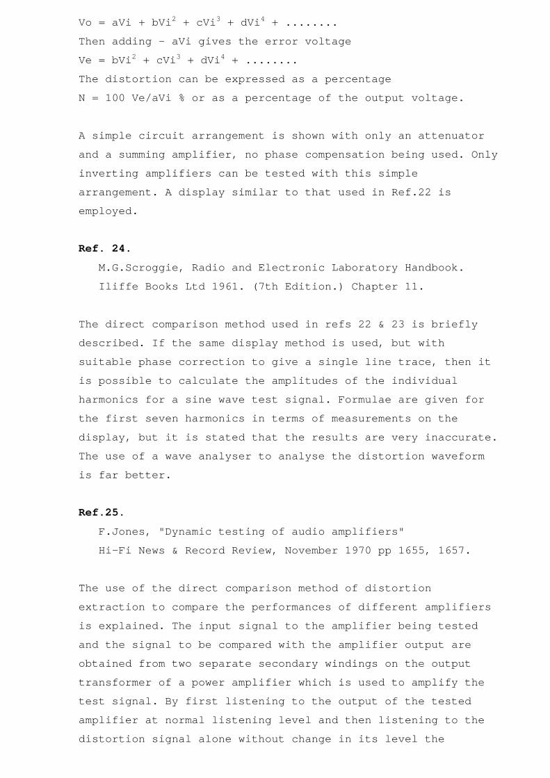
arrangement as shown in Fig.2.1.
FIG. 2.1. Bridge Circuit for Quad II Amplifier Test.
With the switch in position 1 the test signal is obtained at
the output. In position 2 the distortion signal alone is
obtained. In position 3 the amplifier output is obtained. By
passing the output through a further power amplifier to a
loudspeaker the three signals can therefore each be listened
to. By suitable choice of the relative phases of the two
transformer winding outputs either inverting or non-inverting
amplifiers can be tested.
Page 15
Ref.26.
P.Blomley, “New approach to class-B amplifier design."
Wireless World, March 1971.
Reprinted in "High Fidelity Designs.”
(I.P.C. Electrical-Electronic Press Ltd.)
A distortion waveform obtained using the null method at 3kHz at
an amplifier output power level of 10 W is shown and indicates
that measurements of distortion levels less than 0.003 % are
possible. Problems mentioned are the phasing of the signals and
the presence of earth loops and "spurious pick-up
difficulties".
Ref.27.
A.R.Collins, "Testing amplifiers with a bridge."
Audio, March 1972, pp 28 - 32.
Some of the limitations of t.h.d, and i.m.d. tests are given.
The inability to detect dynamic distortions is mentioned and
one of these types of distortion explained. This is known is
"dynamic crossover distortion" and is due to large amplitude
signals causing power dissipation in the output transistors of
a class-B amplifier and a consequent rise in temperature and
increase in collector current for a given bias voltage. The
quiescent current therefore increases and assuming that it had
been adjusted to its optimum value with no signal applied the
crossover distortion will get worse. Crossover distortion tends
to be more significant for small amplitude signals as the
output stage is then operating mainly in its non-linear
crossover region. Therefore a high amplitude signal followed by
a low amplitude signal will cause a rise in crossover
distortion in the low amplitude signal until the output stage
returns to thermal equilibrium. The effect occurs only for
changes in the signal characteristics, hence the name "dynamic"
crossover distortion.
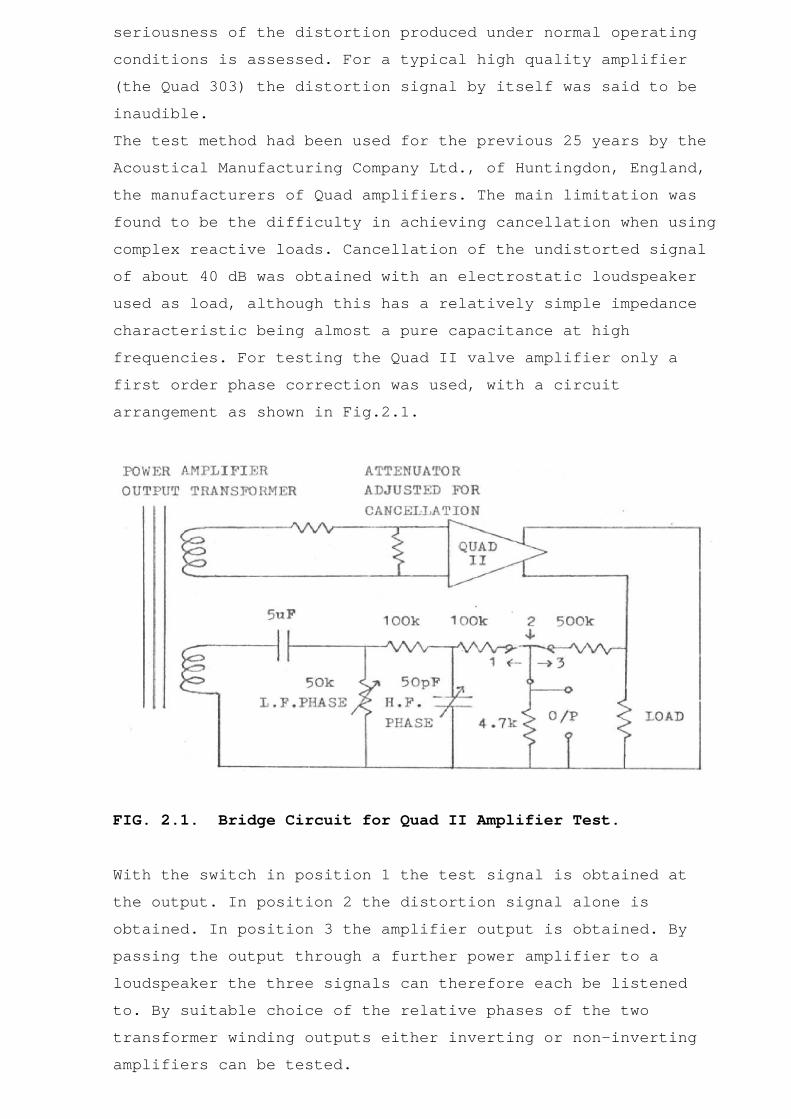
The same test method as that used in Ref.25 is described and a
block diagram of a general purpose testing arrangement given as
shown in Fig.2.2.
Page 16
Fig.2.2. Complete Test Equipment.
A variety of signal sources can be used and the distortion
signal extracted can be displayed on an oscilloscope or
amplified and listened to. The Quad 5OE amplifier shown has an
output transformer with two secondary windings as in ref.25.
Ref.28.
Jan Lohstroh and Matti Otala, "An audio power amplifier for
ultimate quality requirements."
IEEE Transactions on Audio and Electroacoustics,
Vol.AU-21, No.6, December 1973, pp. 545 - 551.
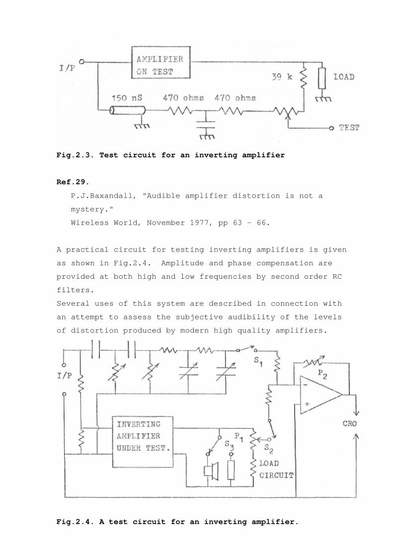
A practical circuit is given for inverting amplifier tests as
shown in Fig.2.3. The component values are chosen for use with
the amplifier design described. A combination of a 150 ns
delay and a first order RC filter provide high frequency
amplitude and phase compensation. Distortion less than 0.01 %
was observed. The majority of the output signal at lower
distortion levels was due to incomplete phase compensation.
Test signals used: sinusoidal, noise and music signal.
Page 17
Fig.2.3. Test circuit for an inverting amplifier
Ref.29.
P.J.Baxandall, "Audible amplifier distortion is not a
mystery."
Wireless World, November 1977, pp 63 - 66.
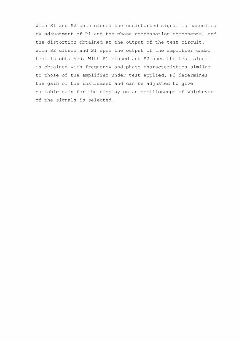
A practical circuit for testing inverting amplifiers is given
as shown in Fig.2.4. Amplitude and phase compensation are
provided at both high and low frequencies by second order RC
filters.
Several uses of this system are described in connection with
an attempt to assess the subjective audibility of the levels
of distortion produced by modern high quality amplifiers.
Fig.2.4. A test circuit for an inverting amplifier.
Page 18
With S1 and S2 both closed the undistorted signal is cancelled
by adjustment of P1 and the phase compensation components, and
the distortion obtained at the output of the test circuit.
With S2 closed and S1 open the output of the amplifier under
test is obtained. With S1 closed and S2 open the test signal
is obtained with frequency and phase characteristics similar
to those of the amplifier under test applied. P2 determines
the gain of the instrument and can be adjusted to give
suitable gain for the display on an oscilloscope of whichever
of the signals is selected.
Page 19
CHAPTER 3.
SOURCES OF ERROR AND THEIR REDUCTION.
3.1 Phase compensation.
The low frequency amplitude and phase response of an amplifier
can be calculated from a knowledge of the component values
used in the amplifier, and a suitable network constructed to
give similar characteristics. Alternatively it may be possible
to modify the amplifier or choose the points in the circuit
from which input and output waveforms are taken to minimise
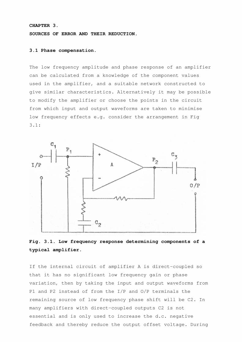
low frequency effects e.g. consider the arrangement in Fig
3.1:
Fig. 3.1. Low frequency response determining components of a
typical amplifier.
If the internal circuit of amplifier A is direct-coupled so
that it has no significant low frequency gain or phase
variation, then by taking the input and output waveforms from
P1 and P2 instead of from the I/P and O/P terminals the
remaining source of low frequency phase shift will be C2. In
many amplifiers with direct-coupled outputs C2 is not
essential and is only used to increase the d.c. negative
feedback and thereby reduce the output offset voltage. During
Page 20
tests it may be possible to short out C2 without interfering
seriously with the operation of the amplifier. There will
still be a small effect due to C3 at low frequencies as it
reduces the output current and therefore reduces the voltage
drop across the output impedance of the amplifier. This effect
can be compensated for as described later in section 5.4. Such
methods are more suited to the design stage than to the
testing of complete amplifiers.
At high frequencies compensation is applied to an amplifier to
maintain stability of the negative feedback loop. The most
common method of maintaining stability is to use a 6 dB/octave
fall in open loop response above a certain frequency giving a
phase lag approaching 90°. Provided the gain round the
feedback loop falls to unity before other phase lags introduce
a further 90° the amplifier will be stable. The open loop
response is then predominantly first order. For measurements
of the highest accuracy the higher order effects must be taken
into account. A closer approximation may therefore be possible
using a second order network.
There will also be a time delay between the input and output
signals, i.e. an extra phase lag with no associated fall in
gain. The relationship between attenuation and phase has been
examined by Bode (Ref.30) who states that a unique relation
exists between any given attenuation characteristic and the
minimum phase shift which must be associated with it. Under
certain conditions an excess phase lag can exist. One such
condition is when the active devices, network elements and
wiring cannot be considered to obey a lumped constant analysis
and the distributed reactances must be taken into account. The
excess phase lag may be regarded as a time delay at a given
frequency, but it is not necessarily the same value of time
delay at all frequencies.
At a given frequency the response of a second order
approximation can be shown to have an amplitude and phase
response equal to that of a first order response plus a time
Page 21
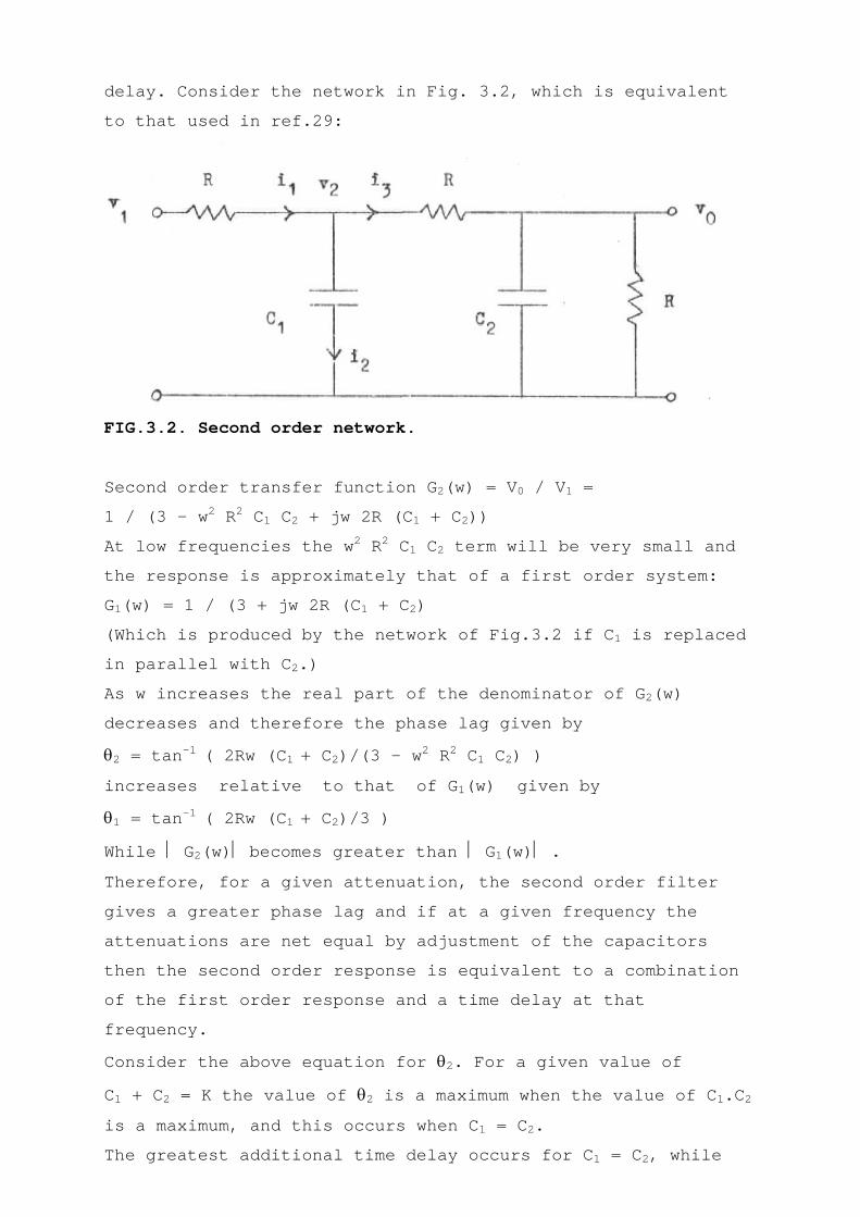
delay. Consider the network in Fig. 3.2, which is equivalent
to that used in ref.29:
FIG.3.2. Second order network.
Second order transfer function G2(w) = V0 / V1 =
1 / (3 – w2 R2 C1 C2 + jw 2R (C1 + C2))
At low frequencies the w2 R2 C1 C2 term will be very small and
the response is approximately that of a first order system:
G1(w) = 1 / (3 + jw 2R (C1 + C2)
(Which is produced by the network of Fig.3.2 if C1 is replaced
in parallel with C2.)
As w increases the real part of the denominator of G2(w)
decreases and therefore the phase lag given by
θ2 = tan-1 ( 2Rw (C1 + C2)/(3 – w2 R2 C1 C2) )
increases relative to that of G1(w) given by
θ1 = tan-1 ( 2Rw (C1 + C2)/3 )
While ⎥ G2(w)⎥ becomes greater than ⎥ G1(w)⎥ .
Therefore, for a given attenuation, the second order filter
gives a greater phase lag and if at a given frequency the
attenuations are net equal by adjustment of the capacitors
then the second order response is equivalent to a combination
of the first order response and a time delay at that
frequency.
Consider the above equation for θ2. For a given value of
C1 + C2 = K the value of θ2 is a maximum when the value of C1.C2
is a maximum, and this occurs when C1 = C2.
The greatest additional time delay occurs for C1 = C2, while
Page 22
none occurs for C1 = 0.
The compensation methods used in refs 28 and 29 could
therefore give identical results at one frequency but would
not match exactly throughout an extended frequency range. In
practice the response of an amplifier being tested will not be
given exactly by either of the two alternatives and therefore
the choice between them can be based on other considerations.
The relative simplicity of providing a second order
compensation network makes this choice more attractive then
the variable time delay solution. Adjustment of C1 and C2 may
be difficult however due to the fact that each affects both
amplitude and phase. In the time delay alternative the time
delay adjustment changes only the phase relationship and there
is therefore less interaction between this adjustment and that
of the first order network.
3.2. Earth connections.
The circuit arrangements shown in refs 28 and 29 are based on
the assumption that what are to be compared are the input and
output voltages relative to the same earth. In practice an
amplifier will have separate input and output earth terminals
and it cannot be assumed that both will be at the same
potential or that any difference will be an undistorted
product of the input signal. One of the possible sources of
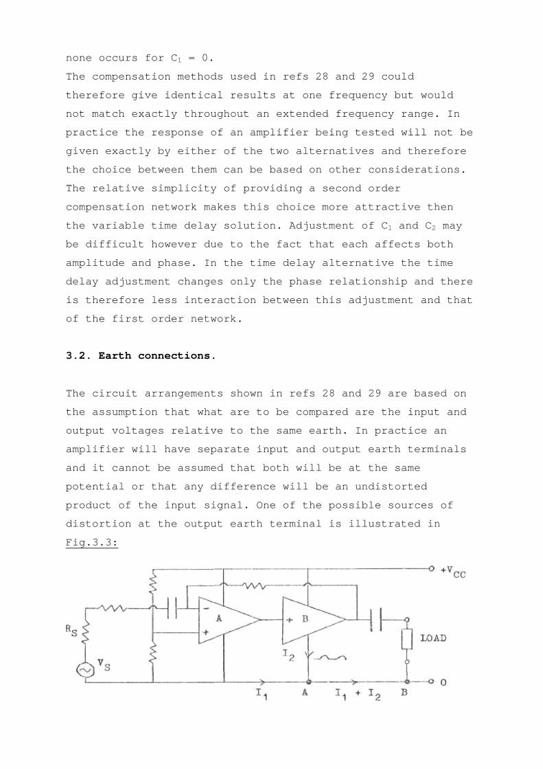
distortion at the output earth terminal is illustrated in
Fig.3.3:
Page 23
The diagram shows a badly chosen circuit arrangement in which
the extremely distorted waveform I2 in the class-B output stage
passes through AB. I2 has peak amplitude about equal to the
peak amplitude of the current through the load. E.g. The peak
current Ip for a sine wave signal is given by:
Power = Ip2 R/2, so at 30W into 8ohms Ip = 2.7Amps.
The connection from A to B may have significant resistance.
For a resistance of 0.1 ohms the peak voltage drop due to 2.7A
would be 0.27 V while the peak voltage across the 8 ohm load
is 21.6 V. The voltage across AB is therefore a significant
percentage of the output signal, about 1.2 %, although this is
not entirely distortion. A test circuit in which the input and
output voltages relative to the input earth were compared
would not reveal the seriousness of this effect. A circuit
arrangement is required in which the potential difference
across the output terminals is compared with the potential
difference across the input terminals.
The arrangement used in ref.25 (see Ch.2) has the required
properties. In this case the input and output signals of the
amplifier being tested are not directly compared. The output
signal is instead compared with a signal obtained from the
same transformer as the input signal. Whether or not the two
signals are sufficiently similar for high accuracy measurement
will depend on the properties of the transformer used. It was
stated in the reference that there was difficulty in
extracting distortion of about 0.1 % when using this type of
circuit. A simple alternative circuit arrangement was designed
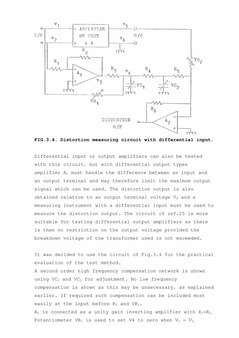
and is shown in Fig.3.4.
In the circuit shown all voltages are measured relative to the
output earth terminal voltage V6. The input differential signal
then becomes (V1 – V6) – (V2 – V6) = V1 – V2 and this is
compared to (V5 –V6)/A. Comparison of the two difference
signals is therefore achieved as required. There is an
additional advantage that similar interference signals picked
up by the two connections to the amplifier input will cancel.
Page 24
FIG.3.4. Distortion measuring circuit with differential input.
Differential input or output amplifiers can also be tested
with this circuit, but with differential output types
amplifier A1 must handle the difference between an input and
an output terminal and may therefore limit the maximum output
signal which can be used. The distortion output is also
obtained relative to an output terminal voltage V6 and a
measuring instrument with a differential input must be used to
measure the distortion output. The circuit of ref.25 is more
suitable for testing differential output amplifiers as there
is then no restriction on the output voltage provided the
breakdown voltage of the transformer used is not exceeded.
It was decided to use the circuit of Fig.3.4 for the practical
evaluation of the test method.
A second order high frequency compensation network is shown
using VC1 and VC2 for adjustment. No low frequency
compensation is shown as this may be unnecessary, as explained
earlier. If required such compensation can be included most
easily at the input before R1 and VR1.
A1 is connected as a unity gain inverting amplifier with R1=R2.
Potentiometer VR1 is used to set V4 to zero when V1 = V2.
Page 25
If A1 gives a gain of exactly -1 then V3 = -V2, and
V4 = 0 for V1 = V2 if VR1 = R3.
The combination of R1, R2, R3, VR1 and A1 acts as a
differential amplifier. There will be very little distortion
added by this circuit when testing inverting amplifiers since
then A1 only amplifies the small difference in potential
between the input and output earth terminals while the full
input signal is only applied to VR1. The use of a standard
differential amplifier in this position would therefore give
an inferior performance unless it was capable of generating as
little distortion as a resistor.
Page 26
3.3. Resistor Characteristics.
A description of the characteristics of the most common types
of resistor is given in Ref.31. There are several of the
characteristics which are relevant to the accuracy of
distortion measurements using the type of instrument to be
described. These are:
1). Voltage coefficient.
Tne resistance of some types of resistor can change
significantly as a result of an applied voltage. The voltage
coefficients of carbon composition and carbon film resistors
are given as typically 3000 and 100 parts per million per
volt respectively. I.e. For a 1 V amplitude signal applied
the incremental resistance will change by 0.3 % and 0.01 %
respectively. These changes would have a significant effect
on the signal cancellation if they occurred in R3, VR1, R4, R5,
or VR2 in Fig.3.4. R1 and R2 are of equal value and have equal
voltages applied. They give a gain of R2/R1 for amplifier A1
and therefore provided R1 and R2 have similar properties they
will not introduce large errors.
There are other types of resistor which have negligible
voltage coefficients. These include metal oxide, cermet and
metal film types. Wirewound resistors also have very small
voltage coefficients but may have significant reactive
components depending on the winding technique used in their
construction.
2). Thermal effects.
The temperature coefficients of metal oxide, cermet and metal
film resistors are given as 50 to 250, 100 and 15 to 100
ppm/0C respectively. When a signal is applied across a
resistor its temperature changes due to the power
dissipated. Ref.31 gives typical graphs of temperature change
as a function of power dissipation. The relationship is
linear over the temperature range shown with a 1/2 W resistor
increasing in temperature by 50 °C at 1/2 W dissipation. The
change is therefore 100 °C per W. For a temperature
Page 27
coefficient of 100 ppm/°C the change is therefore 104 ppm/W.
e.g. A 2k ohm resistor with 1 V applied dissipates 1/2000 W,
The incremental resistance will therefore change by 0.0005%.
For measurements using constant amplitude test signals such
changes can be compensated for by adjustment of the
potentiometers in Fig.3.4. When varying amplitude or very low
frequency test signals are used the thermal effects may
become significant, so the resistors and potentiometers
should be low temperature coefficient types. Metal film and
metal oxide fixed resistors and cermet potentiometers are
readily available and are therefore to be recommended in this
application. The use of resistors with high specified maximum
power dissipation will also reduce the thermal effects. The
most critical resistance in Fig.3.4 is VR2 which has the full
output of the amplifier applied across it. For testing high
power amplifiers therefore particular attention must be paid
to the thermal properties of VR2.
3). Resistor noise.
A resistor produces thermal noise and current noise. The
thermal noise voltage is a function of temperature,
resistance and bandwidth and is independent of the applied
signal except for the effect of the resulting temperature
change. Thermal noise will be considered later (Section 4.4)
Current noise is a function of the applied signal voltage.
The typical total current noises for metal oxide, cermet and
metal film resistors are given as O.O3, 0,4 to 1.0 and
0.015 µV/V respectively. The use of metal film or metal oxide
resistors will therefore give negligible current noise. Even
cermet types will give noise less than 0.0001 % of the
applied voltage.
Measurement of third harmonic distortion generated by solid
carbon, carbon film and metal film resistors has been made by
Takahisa, Yanagisawa and Shiomi (Ref.32). They suggest that
in general passive elements have non-linear V – I
characteristics due to the presence of electrode contacts and
potential barriers in the current path.
Page 28
The third harmonic voltage was found to be proportional to
(J1n L /Dm) where J1 is the current density of the
fundamental (10 kHz was used), L is the length and D the
thickness of the film. n is between 2.2 and 2.8 and
m = 3.0 for a metal film resistor.
For 250 kohm resistors with a 250 V signal applied the third
harmonic voltages were:
Metal film (1/2 W) 0,03 to 0.15 mV = 0.12 to 0.6 ppm.
Carbon film (1/2 W) 1.5 to 4.0 mV = 6.0 to 16 ppm.
Solid carbon (1/4 W) 400 to 800 mV = 0.16 to 0.32 %.
The fourth, fifth and sixth harmonics are shown for a high
distortion carbon film resistor sample as - 60 dB, - 26 dB
and - 74 dB respectively relative to the third harmonic.
The inferior performance of carbon resistors is confirmed by
these results.
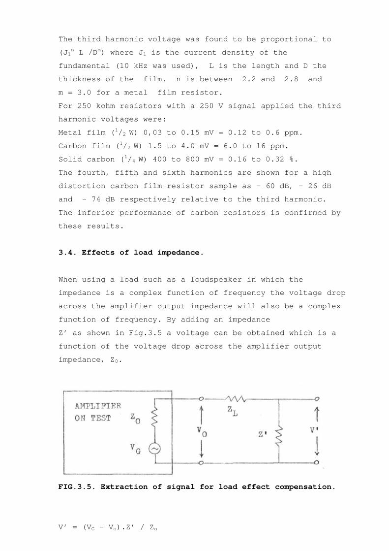
3.4. Effects of load impedance.
When using a load such as a loudspeaker in which the
impedance is a complex function of frequency the voltage drop
across the amplifier output impedance will also be a complex
function of frequency. By adding an impedance
Z’ as shown in Fig.3.5 a voltage can be obtained which is a
function of the voltage drop across the amplifier output
impedance, Z0.
FIG.3.5. Extraction of signal for load effect compensation.
V’ = (VG – Vo).Z’ / Zo
Page 29
Therefore Vo + V’.Zo / Z’ = VG
By adding + V’.Zo / Z’ to Vo the amplifier output voltage
can be obtained without its load dependence. I.e. the open
circuit output voltage VG is obtained.
In general Zo will not be linear. The non-linear component ZD
generates distortion, which it is required to measure, and
therefore there is no need to compensate for this.
If Zo = ZLIN + ZD where ZLIN is the linear component of Zo then
it is ZLIN which must be compensated for, and V’.ZLIN /Z’ must
be added to Vo to achieve this.
The value of ZLIN is not, however a constant. Suppose the
voltage drop across Zo is given by:
V = Z1I + Z2I2 + Z3I3 + ....... ........Equ.3.1
For a current A sin(wt) the first three terms give:
V = AZ1 sin(wt) + A2Z2(1 – cos(2wt))/2
+ A3Z3(3sin(wt) – sin(3wt)/4
I.e. the undistorted component is:
(AZ1 + 3A3Z3 /4)sin(wt)
If ZLIN is defined as the ratio of undistorted voltage to
current then ZLIN = Z1 + 3A2Z3 /4.
I.e. ZLIN is a function of signal amplitude A,
The compensation can therefore only he carried out at a
single signal amplitude using linear components for Z’. At
other amplitudes an undistorted signal component will remain.
The effectiveness of this method is therefore dependent on
the degree and type of non-linearity of Zo. The even order
terms in the power series (Equ.3.1) do not contribute an
indistorted component and it is the odd order coefficients Z3,
Z5, Z7 etc. which are relevant.
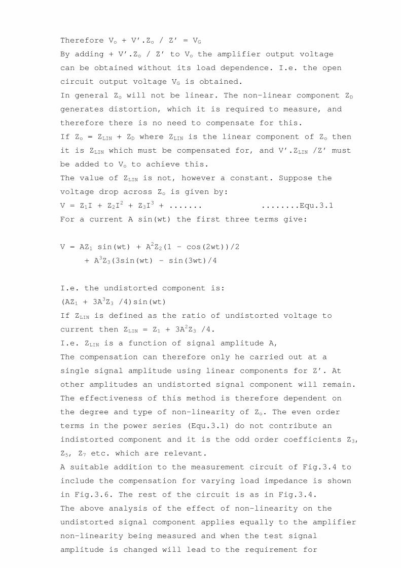
A suitable addition to the measurement circuit of Fig.3.4 to
include the compensation for varying load impedance is shown
in Fig.3.6. The rest of the circuit is as in Fig.3.4.
The above analysis of the effect of non-linearity on the
undistorted signal component applies equally to the amplifier
non-linearity being measured and when the test signal
amplitude is changed will lead to the requirement for
Page 30
readjustment of the test circuit for optimum signal
cancellation. What is then being done is in effect to select
the best straight line through the transfer characteristic
rather than regard all non-linear power series terms as
distortion. (Ref.23)
FIG.3.6. Load effect compensation addition.
The output of A2 resulting from V5 and V7 is:
R6V5 /VR2 + R6V7 /VR3
It is required to add V7 ZLIN /Z’ to V5 and therefore
it is required that the output becomes :
R6 (V5 + ZLIN.V7 /Z’)/ VR2
It is therefore required that
Z’ / VR3 = ZLIN / VR2
If ZLIN has reactive components and it is required that Z’ is
small then it will be more convenient to use a small value
resistance (say 0.1 ohms) for Z’ and add the reactive
compensation components to VR3. As VR3 will be relatively
large only small capacitances will generally be needed to
give the necessary results.
In general the output impedance of an amplifier will increase
at high frequencies due to the fall in overall negative
feedback. As the output impedance is reduced by a factor
Page 31
(1 – AB) where A is the open loop gain and B the feedback
network gain it is possible for the output impedance to have
a negative real part if the real part of AB becomes more than
+1. This can only occur for phase lags in the gain round the
feedback loop of more than 900 and is therefore unlikely to
happen within the audio frequency range when using the usual
first order high frequency compensation. If it did occur then
it would be necessary to use a different arrangement to that
of Fig.3.6. E.g. a proportion of V7 could be taken via an
inverting amplifier to the input of A2 to give a subtraction
from V5 instead of an addition.
Sometimes an amplifier is intentionally designed to have a
negative output resistance at low frequencies to give better
damping of a loudspeaker resonance. This effect is produced
by the use of positive current feedback.
The easiest way to avoid having to compensate for a negative
output resistance is to add a small resistor in series with
the amplifier output equal to or greater than the largest
negative value of the real part of Z0 within the frequency
range of interest. This resistor can then be treated as part
of Z0, and V5 obtained from the end of the resistor connected
to the load. The effective output resistance is then never
negative within the frequency range used.
To set up the circuit balance, VR2 should be adjusted for
cancellation of the undistorted signal with the load
disconnected (then V7 = 0). Connection of the load will then
introduce an additional undistorted signal component due to
the voltage drop across Z0. This can be eliminated at a given
signal amplitude (for a sine wave signal) by adjustment of
the values of VR3 and Z’.
In the above analysis it has been assumed that VR2 >> ZL and
ZR3 >> Z’ so that VR2 and VR3 do not significantly alter the
voltages being measured. This condition will usually be met
when measuring power amplifiers.
To use the above compensation method it is convenient to
measure Z0 and provided this has only a small non-linear
Page 32
component this can be done by first balancing the circuit of
Fig.3.4 with no load connected and using a sine wave signal.
Addition of a resistive load RL of known value will give a
voltage drop across Z0, which will be amplified by A2. Provided
the voltage drop is significantly greater than the amplifier
distortion it can be compared in amplitude and phase with the
signal across RL by displaying both signals on a dual trace
oscilloscope. The gain and phase shift of A2 must be taken
into account. Knowing the voltage drop across Z0 for a given
voltage across RL the value of Z0 can be calculated at the
frequency used since the current through Z0 is the same as
that through RL.
Plotting Z0 against frequency will make it possible to work
out the value of Z0 as a function of frequency and derive
suitable component values for Z’ and VR3.
Many power amplifiers include components in their output
circuit to assist in the high frequency stabilisation when
using capacitive loads or to protect the output stage against
the effects of an inductive load. An output coupling
capacitor is also used in some circuits. The effects of all
these components can be eliminated by including them as part
of the load as shown in Fig.3.7.
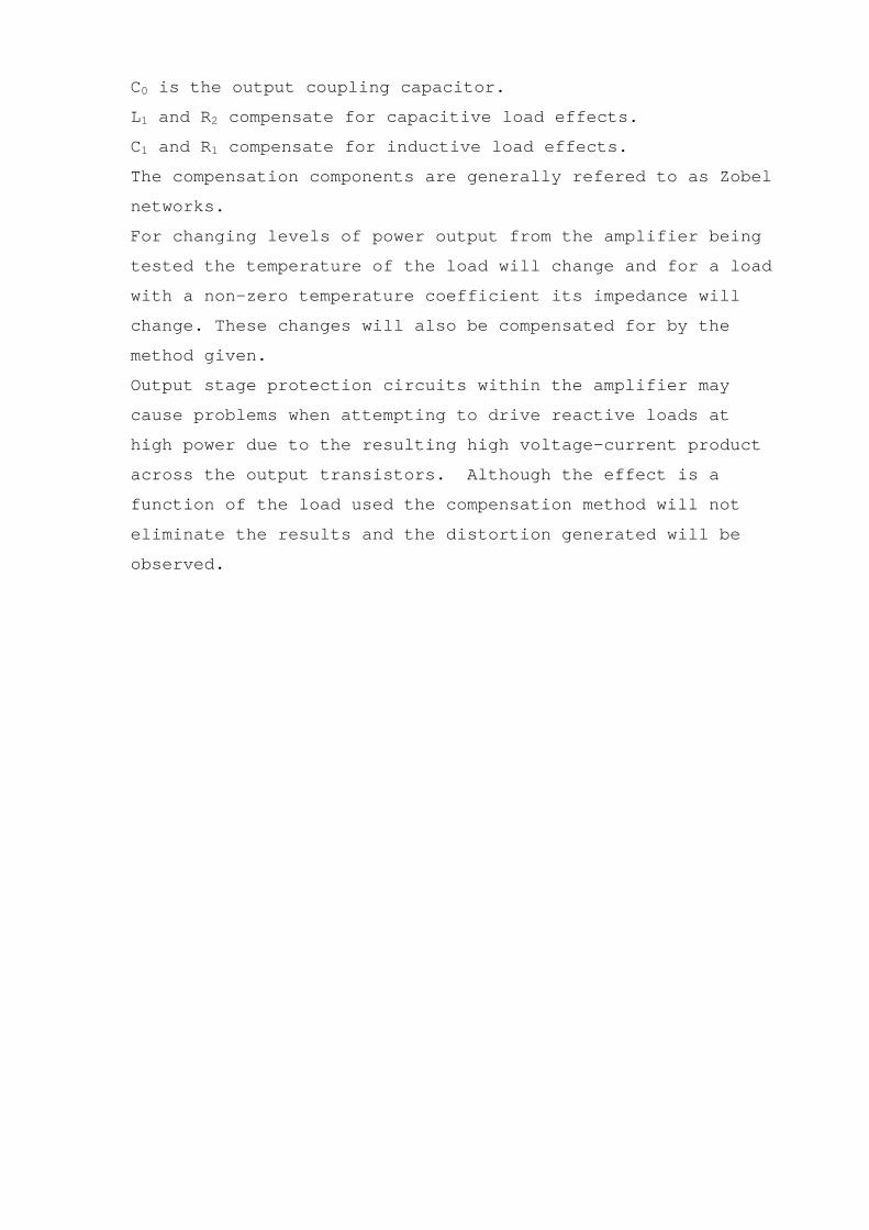
FIG.3.7. Output component effect elimination.
Page 33
C0 is the output coupling capacitor.
L1 and R2 compensate for capacitive load effects.
C1 and R1 compensate for inductive load effects.
The compensation components are generally refered to as Zobel
networks.
For changing levels of power output from the amplifier being
tested the temperature of the load will change and for a load
with a non-zero temperature coefficient its impedance will
change. These changes will also be compensated for by the
method given.
Output stage protection circuits within the amplifier may
cause problems when attempting to drive reactive loads at
high power due to the resulting high voltage-current product
across the output transistors. Although the effect is a
function of the load used the compensation method will not
eliminate the results and the distortion generated will be
observed.
Page 34
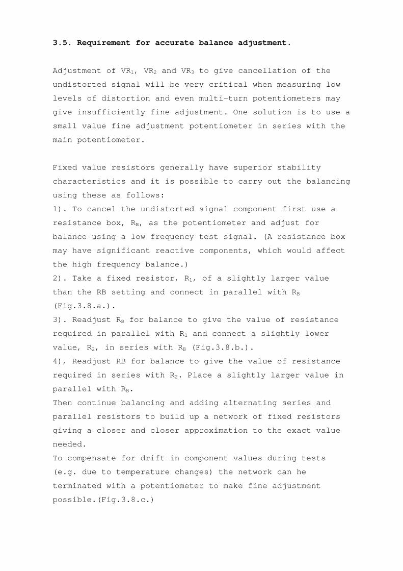
3.5. Requirement for accurate balance adjustment.
Adjustment of VR1, VR2 and VR3 to give cancellation of the
undistorted signal will be very critical when measuring low
levels of distortion and even multi-turn potentiometers may
give insufficiently fine adjustment. One solution is to use a
small value fine adjustment potentiometer in series with the
main potentiometer.
Fixed value resistors generally have superior stability
characteristics and it is possible to carry out the balancing
using these as follows:
1). To cancel the undistorted signal component first use a
resistance box, RB, as the potentiometer and adjust for
balance using a low frequency test signal. (A resistance box
may have significant reactive components, which would affect
the high frequency balance.)
2). Take a fixed resistor, R1, of a slightly larger value
than the RB setting and connect in parallel with RB
(Fig.3.8.a.).
3). Readjust RB for balance to give the value of resistance
required in parallel with R1 and connect a slightly lower
value, R2, in series with RB (Fig.3.8.b.).
4), Readjust RB for balance to give the value of resistance
required in series with R2. Place a slightly larger value in
parallel with RB.
Then continue balancing and adding alternating series and
parallel resistors to build up a network of fixed resistors
giving a closer and closer approximation to the exact value
needed.
To compensate for drift in component values during tests
(e.g. due to temperature changes) the network can he
terminated with a potentiometer to make fine adjustment
possible.(Fig.3.8.c.)
Page 35
FIG.3.8. Successive approximation resistor adjustment.
Page 36
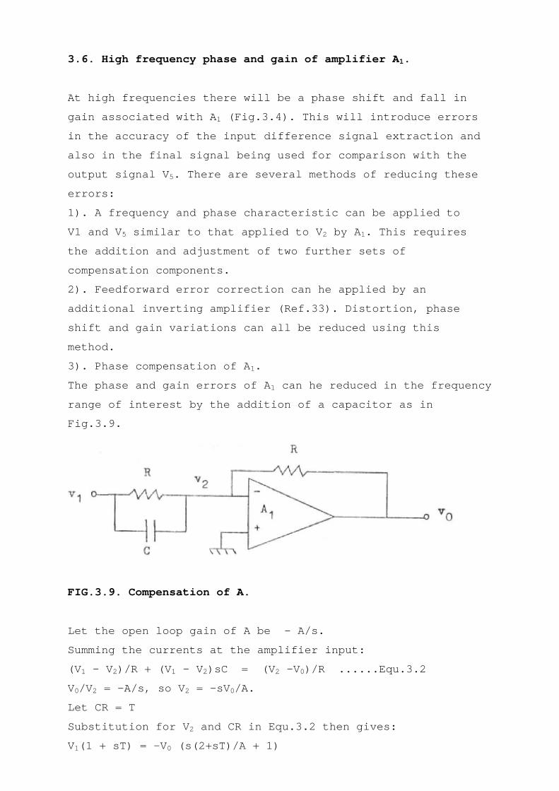
3.6. High frequency phase and gain of amplifier A1.
At high frequencies there will be a phase shift and fall in
gain associated with A1 (Fig.3.4). This will introduce errors
in the accuracy of the input difference signal extraction and
also in the final signal being used for comparison with the
output signal V5. There are several methods of reducing these
errors:
1). A frequency and phase characteristic can be applied to
V1 and V5 similar to that applied to V2 by A1. This requires
the addition and adjustment of two further sets of
compensation components.
2). Feedforward error correction can he applied by an
additional inverting amplifier (Ref.33). Distortion, phase
shift and gain variations can all be reduced using this
method.
3). Phase compensation of A1.
The phase and gain errors of A1 can he reduced in the frequency
range of interest by the addition of a capacitor as in
Fig.3.9.
FIG.3.9. Compensation of A.
Let the open loop gain of A be - A/s.
Summing the currents at the amplifier input:
(V1 – V2)/R + (V1 – V2)sC = (V2 –V0)/R ......Equ.3.2
V0/V2 = -A/s, so V2 = -sV0/A.
Let CR = T
Substitution for V2 and CR in Equ.3.2 then gives:
V1(1 + sT) = -V0 (s(2+sT)/A + 1)
Page 37
∴-V0/V1 = (1 + sT)/(1 + s(2 + sT)/A)
= (1 + jwT)/(1 – w2T/A + jw2/A)
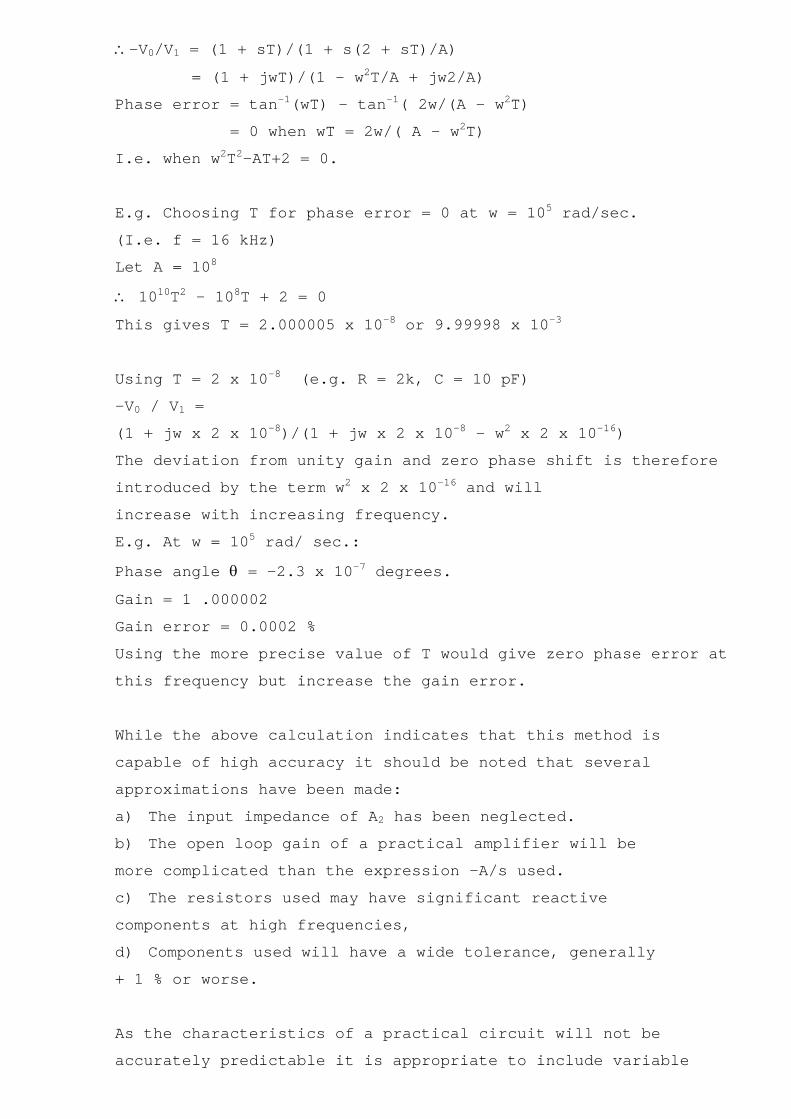
Phase error = tan-1(wT) – tan-1( 2w/(A – w2T)
= 0 when wT = 2w/( A – w2T)
I.e. when w2T2–AT+2 = 0.
E.g. Choosing T for phase error = 0 at w = 105 rad/sec.
(I.e. f = 16 kHz)
Let A = 108
∴ 1010T2 – 108T + 2 = 0
This gives T = 2.000005 x 10⁻⁸ or 9.99998 x 10⁻³
Using T = 2 x 10⁻⁸ (e.g. R = 2k, C = 10 pF)
-V0 / V1 =
(1 + jw x 2 x 10⁻⁸)/(1 + jw x 2 x 10⁻⁸ – w2 x 2 x 10-16)
The deviation from unity gain and zero phase shift is therefore
introduced by the term w2 x 2 x 10-16 and will
increase with increasing frequency.
E.g. At w = 105 rad/ sec.:
Phase angle θ = -2.3 x 10⁻⁷ degrees.
Gain = 1 .000002
Gain error = 0.0002 %
Using the more precise value of T would give zero phase error at
this frequency but increase the gain error.
While the above calculation indicates that this method is
capable of high accuracy it should be noted that several
approximations have been made:
a) The input impedance of A2 has been neglected.
b) The open loop gain of a practical amplifier will be
more complicated than the expression –A/s used.
c) The resistors used may have significant reactive
components at high frequencies,
d) Components used will have a wide tolerance, generally
+ 1 % or worse.
As the characteristics of a practical circuit will not be
accurately predictable it is appropriate to include variable
Page 38
adjustments to compensate for the unknown factors. A variable
capacitor can be used for C and adjusted to give good common
mode rejection for high frequencies in the differential input
stage formed by A1, R1, R2, R3 and VR1 (Fig.3.4).
If the two inputs are connected together, and a low frequency
signal applied to them, then VR1 can be adjusted to give
cancellation of the signal at A2 output.
With a high frequency signal (about 20 kHz) applied the variable
capacitor connected across R1 can be adjusted to give the best
cancellation of this signal.
The inclusion of C changes the phase versus gain characteristics
of the A1 feedback loop and must be taken into account when
calculating the high frequency compensation necessary for
stability.
Due to its simplicity it was decided to use this method of
compensation in the practical design to be produced.
Page 39
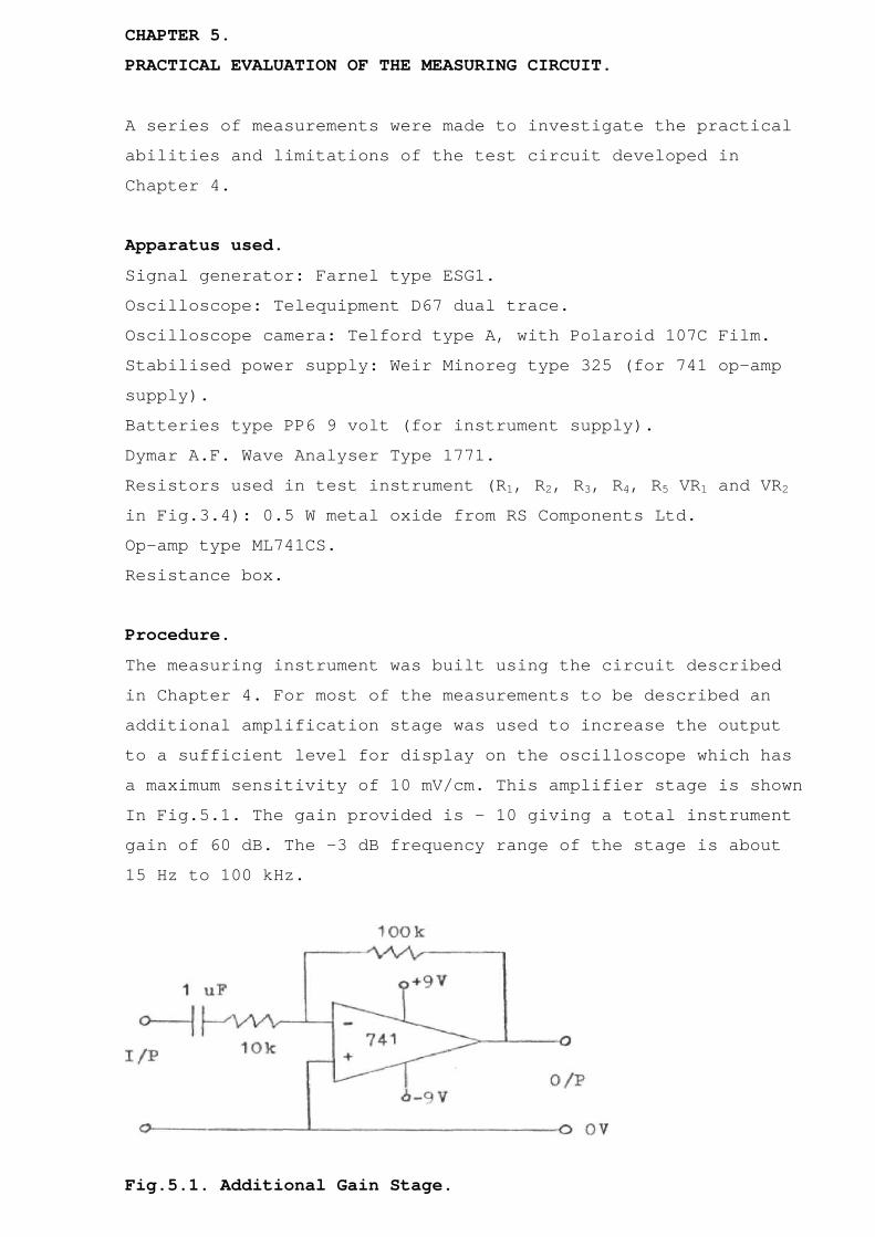
CHAPTER 4. MEASURING INSTRUMENT CIRCUIT DESIGN.
4.1. Unity Cain Inverting Amplifier A1.
The requirements for A1 (Fig.3.4) are that it has low
distortion, low noise and give a constant gain throughout the
audio frequency range. The maximum signal amplitude to be
handled depends on the input signal required by the amplifier
being tested to give its maximum output. A value of 1V peak
amplitude will be used for the analysis of the distortion of
the design to be produced.
There are many small signal amplifiers available in integrated
circuit form, designed with emphasis on a variety of
parameters such as low frequency gain, noise, bandwidth,
distortion, common mode rejection etc. The performance with
regard to distortion of several integrated circuit amplifiers
has been compared, (Ref.34, 35). The 741, LM3O1 and uA739 were
tested with closed loop gains of -3. The uA739 gave the lowest
distortion level of 0.013% at an output of 1V r.m.s. at
20 kHz, reducing at lower frequencies. Figures given for a
simple three transistor discrete component amplifier in Ref.34
showed that under similar conditions a distortion level only a
third that of the uA739 was produced. Clearly the use of this
integrated circuit would severely limit the usefulness of the
instrument for testing low distortion amplifiers. It would be
possible to use two amplifiers in a feedforward error
correction circuit as in Ref.33, but it was decided to use a
discrete component amplifier designed to optimise the
parameters of interest in this application.
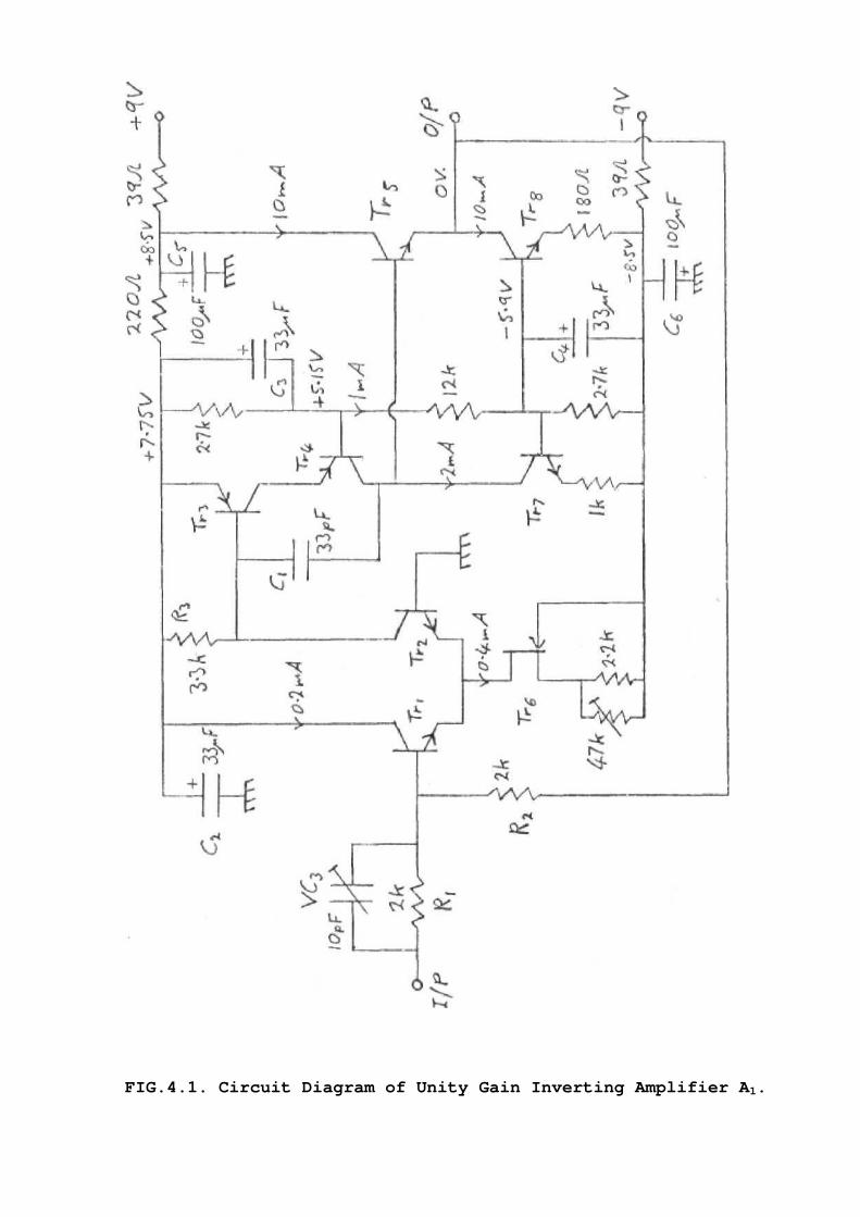
The design finally produced is shown in Fig.4.1.
Page 40
FIG.4.1. Circuit Diagram of Unity Gain Inverting Amplifier A1.
Page 41
Tr6, Tr7 and Tr8 act as current sources.
The transistors used should be low noise types and the ones
chosen were:
npn: BC169C (hfe = 450 to 900 at IC = 2 mA, VCE = 5V)
pnp : BC259B (hfe = 240 to 500 at IC = 2 mA, VCE = 5V).
VC3 provides gain and phase correction as described in section
3.6, while C1 gives high frequency negative feedback loop
stability. As the open loop gain falls at 6 dB/octave at high
frequencies the amount of overall negative feedback reduces and
distortion is consequently reduced less. Calculation of
distortion will therefore be made at the top end of the audio
frequency range (20 kHz) to give a worst case figure.
Each stage will now be considered separately. Only an
approximate analysis will be given, as all the factors affecting
performance are not known to a high degree of accuracy.
4.1.1. Differential Input Stage Analysis.
Distortion.
The distortion of this type of stage is analysed in Ref.36 where
it is shown that minimum distortion occurs for equal collector
currents in the two transistors. The distortion is then
predominantly third harmonic and is less than 0.005% for a peak
sine wave input amplitude of 1 mV if the collector currents are
matched to within 0.6%. For an output of 1V peak amplitude the
gain from Tr1 base to the output of the amplifier must be 1000 at
20 kHz if the input signal is to be 1 mV at this frequency. This
value of gain was chosen for the design.
The expression used for the gain in section 3.6 was –A/s. For
modulus of gain = 1000 at 20 kHz this gives:
A = 1000 x 2π x 2 x 104 = 1.2 x 10⁸. The value of 108 used for A
in the calculation of VC3 was therefore sufficiently accurate as
this is a variable component.
Page 42
Noise.
Graphs of noise figure against IC are given for the BC169C
transistor in Ref.37. At 10 kHz a noise figure of 0.5 dB is
obtained at IC = 0.2 mA, and a source resistance of 1 kohm. Using
R1 = R2 = 2 kohm to give this source resistance, Tr1 will only
increase the effective input noise by 0.5 dB while Tr2 will
contribute even less as its equivalent input noise current
generator is effectively shorted and only its noise voltage
contributes. (Ref.38). The contribution of the transistors to
the noise voltage of the complete circuit will be neglected.
Frequency Response.
At IC = 0.2 mA ft is given as 60 MHz at VCE = 10V.
Tr2 operates as a common base stage and therefore will have a
current gain only a little less than unity up to 60 MHz, Tr1 is a
common-collector stage and has an input impedance which falls at
high frequencies due to the presence of input capacitances CCB
and CBE.
CCB is given as 2.7 pF at VCB = 10V and CBE can be calculated from
the formula:
FT = 1/2πCBERe where Re = 25/IE ohms. (IE in mA)
Taking fT = 60 MHz, IE = 0.2 mA gives CBE = 21 pF.
The signal voltage VE at the emitter of Tr1 is half the input
voltage at the base, VB.
As a result of this only half the input voltage appears across
CBE and it takes a current equal to that which would be taken by
CBE/2 connected from base to earth . The total effective input
capacitance is therefore:
CIN = CCB + CBE/2 = 13pF.
The effect of this on the overall negative feedback of A1 can be
seen from Fig.4.2 where R1 and R2 have been replaced by their
Thevenin equivalent and the signal source impedance taken as
zero.
Page 43
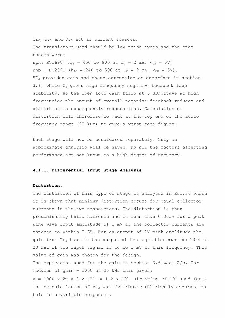
FIG.4.2. Effect of Input Capacitance on the Feedback.
CIN = 13pF and VC3 = 10 pF (see Section 3.6)
The feedback network response is therefore that of a first order
low pass filter with gain 0.5 /(1 + jw/wo)
Where wo = 1 / 103(C1 + CIN)
∴f0 = w0/2π = 7 MHz.
There is therefore a 45° phase lag and a gain of - 9 dB
at 7 MHz due to the feedback network. The open loop gain of
-1.2x10⁸/s chosen in Section 4.1.1. gives a gain of 8.7 dB and a
phase lag of 90° at 7 MHz. The total gain round the feedback
loop at this frequency is about unity while the phase lag is
135°. As the gain has fallen to unity before the phase lag has
reached 180o the amplifier will be stable.
4.1.2. Cascode Stage Tr3, Tr4.
a) Introduction. In this part of the circuit Tr4 operates in
common base mode and has a low input impedance giving Tr3 a low
impedance collector load. The voltage gain of Tr3 is -1 since Tr3
and Tr4 have approximately equal emitter currents and therefore
approximately equal base to emitter voltages. The low voltage
gain of Tr3 reduces distortion due to the dependence of the
output admittance, hoe on VCE.
The base to collector capacitance of Tr3 is a function of
VCE and therefore will introduce distortion. A high voltage gain
for Tr3 would increase the effect of this non-linear capacitance
due to the Miller Effect.
The output admittance of the common base stage Tr4 is given by
hob = hoe / hfe. The input impedance of Tr5 is given by hfeRL.
For BC259B transistors (Ref.37) hfe = 240 to 500 and
Page 44
hoe < 70 µS (both at 1 kHz).
∴1/hob > 3.4 MΩ
For a total output load for Tr5 of 1 kohm given by the 2k
feedback resistor in parallel with the 2k load resistance to be
used, the input resistance of Tr5 is greater than 450k.
b) Open Loop Gain.
C1 is chosen to give the required open loop gain of 1000 at 20
kHz. The signal current through C1 is approximately equal to the
collector signal current of Tr2 at 20 kHz.
∴ The voltage gain is given by gm1 x 1/jwC1, where gm1 is the
mutual conductance of the input stage.
gm1 = 1/2Re = 4mS.
∴ At 20 kHz for a voltage gain of modulus 1000:
(4x10⁻³)/(2π x 2 x 104 x C1) = 1000
∴C1 = 33pF.
c) Distortion.
The value of R3 is given by the collector current of Tr2 (0.2mA)
and VBE of Tr3 (0.64V) as 3.3k
(Neglecting the base current of Tr3).
Input impedance of Tr3 at IC = 2 mA is given by hfe Re.
Re = 25/IE ohms.
Using the minimum value of hfe for the BC259B of 240 gives a
total input impedance including R3 of about 1.6k.
The minimum impedance at Tr4 collector is 3.4M in parallel with
450k (Section 4.1.2.a).) and the impedance of the current source
Tr7.
For the BC169C transistor used as Tr7, hoe < 110 µS and
Hfe > 450, ∴1/hob > 4M.
The total impedance at Tr4 collector is therefore a minimum of
360k. The minimum open loop voltage gain of the stage with C1
disconnected is gm RL = IE x 360 x 103 /25.
With IE = 2 mA this becomes 28800.
The feedback loop therefore can he represented by the equivalent
Page 45
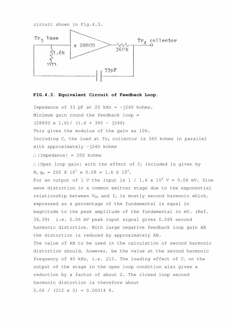
circuit shown in Fig.4.3.
FIG.4.3. Equivalent Circuit of Feedback Loop.
Impedance of 33 pF at 20 kHz = -j240 kohms.
Minimum gain round the feedback loop =
(28800 x 1.6)/ (1.6 + 360 – j240)
This gives the modulus of the gain as 106.
Including C1 the load at Tr4 collector is 360 kohms in parallel
with approximately -j24O kohms
∴|Impedance| = 200 kohms
∴|Open loop gain| with the effect of C1 included is given by
RL gm = 200 X 103 x 0.08 = 1.6 X 10⁴.
For an output of 1 V the input is 1 / 1.6 x 10⁴ V = 0.06 mV. Sine
wave distortion in a common emitter stage due to the exponential
relationship between VBE and IC is mostly second harmonic which,
expressed as a percentage of the fundamental is equal in
magnitude to the peak amplitude of the fundamental in mV. (Ref.
36,39) i.e. 0.06 mV peak input signal gives 0.06% second
harmonic distortion. With large negative feedback loop gain AB
the distortion is reduced by approximately AB.
The value of AB to be used in the calculation of second harmonic
distortion should, however, be the value at the second harmonic
frequency of 40 kHz, i.e. 212. The loading effect of C1 on the
output of the stage in the open loop condition also gives a
reduction by a factor of about 2. The closed loop second
harmonic distortion is therefore about
0.06 / (212 x 2) = 0.00014 %.
Page 46
4.1.3. Output Stage.
This stage adds distortion due to the exponential relationship
between VBE and IC.
At collector current IC in mA, gm = IC / 25 S.
For RL = 1k and a 1V signal applied IC changes by a value of 1mA.
gm = dIC / dVBE, so change in VBE = 10-3/gm = 25 x 10-3 /IC.
Percentage second harmonic distortion = VBE in mV = 25/IC %
This is, however, a percentage of VBE.
As a percentage of the 1 V output signal: Second harmonic
distortion = 25 x 25 x 10-3/IC2 = 0.625/IC2 % (IC in mA).
For IC = 10 mA second harmonic distortion = 0.006 %.
4.1.4. Total Distortion.
There are several sources of distortion (Ref.42) which have not
been considered. These include the variations of barrier and
diffusion capacitances in the transistors resulting from changes
in VCB and IC respectively, and changes in hfe resulting from
changes in VCB and IC. At low frequencies thermal modulation
effects may also become significant. (Ref.43) Rough calculations
suggest that the most important of these is the change in hfe of
Tr5 due to its changing VCB. This gives second harmonic
distortion of the order of 0.001 %.
The total r.m.s. distortion depends on the relative phases of
the separate components at each harmonic. The worst case figure
is the sum of the individual components. The second harmonic
distortion derived for Tr3 (0.00014 %) and Tr5 (0.006 % and
0.001%) for a 20 kHz signal give a maximum total of about
0.007%. The overall negative feedback loop gain is about 250 at
40 kHz and therefore the total closed loop second harmonic
distortion will be a maximum of about (0.007 / 250)% = 0.00003%.
The third harmonic distortion of the input stage (0.005 %) is
reduced by the -6 dB/ octave response of the second stage and
the feedback loop gain (167 at 60 kHz) to about 0.00001 %. Total
r.m.s. distortion D = ( d22 + d32 )1/2 where d2 and d3 are second
Page 47
and third harmonic percentages respectively. The total r.m.s.
harmonic distortion at an input signal frequency of 20 kHz and
an output peak amplitude of 1 V is therefore a maximum of about
0.000032 %.
In general in class-A amplifiers second harmonic distortion is
proportional to the signal amplitude while the third harmonic
distortion is proportional to the square of the signal
amplitude.(Ref.39)
4.1.5.Circuit Details.
The source of Tr6 is shown with a variable resistance connected.
As the distortion produced by the input stage is critically
dependent on the matching of the collector currents of Tr1 and
Tr2 the optimum current through Tr6 is most easily set by
adjusting it to give minimum total amplifier distortion. By
applying a sine wave common mode signal to the differential
input stage of the measuring instrument (i.e. applied to R1 and
VR1 in Fig.3.4.) the input signal can be cancelled to leave a
signal which includes the distortion of A1. Adjustment of the
current through Tr6 alters the second harmonic distortion and
therefore by observing the amplitude of the total distortion at
the output of A2 the optimum current can be set. A field effect
transistor current source was used rather than a further bipolar
transistor similar to Tr7 and Tr8. This was done because a
battery supply was used to give low hum and noise and
consequently the supply voltage reduced slowly with time and the
resistive bias arrangement used for Tr7 and Tr8 bases gave slowly
changing collector currents. Also it was found that when using
three bipolar transistors as current sources with their bases
biased by the same resistive voltage divider the amplifier had
two stable states. On being connected to the power supply it
went into one of these states in which the output voltage
becomes about – 8V. Shorting the bases to the 0V 1ine for a
moment triggered the circuit into the required operating
condition with a 0V output for no input signal. The effect was
caused by Tr8 taking a large base current until its VCE increased
sufficiently for the current gain to become significant. The
Page 48
resulting low base voltage on the input stage current source
transistor prevented it from conducting sufficiently to make
Tr2, Tr3, Tr4 and Tr5 conduct and increase VCE of Tr8. The negative
output state was consequently stable. The use of a field effect
transistor for Tr6 completely solved the problem.
The approximate source resistance required by Tr6 was calculated
by first measuring IDSS and VP for the device used (an E202 type).
A Tektronix Type 576 Curve Tracer was used and values of IDSS =
1.71 mA and VP = 1.4 V obtained.
Using the formula ID = IDSS ( 1 – VGS/VP )2 :
VGS = 0.72 V at ID = 0.4 mA.
∴ Source resistance required =(0.72 / 0.4)k =1.8k. A value of
2.2k in parallel with a 47k preset potentiometer was used.
The voltage and current levels relevant to the choice of
resistor values are shown in Fig.4.1 together with the nearest
standard values of resistance corresponding to these levels. As
the transistors used are all very high current gain types the
base currents are very small and have been ignored.
C3 and C4 ensure that Tr4, Tr7 and Tr8 operate in common base mode
by effectively earthing the bases at frequencies within the
audio range. The capacitor values are not critical and were
chosen as 33µF. As electrolytic capacitors have significant
impedance at very high frequencies a small value ceramic disc
capacitor (0.02µF) was connected in parallel with each
electrolytic to maintain a low impedance. The supply decoupling
capacitors C2, C5 and C6 were included to prevent interaction via
the supply connections with other sections of the test
instrument. The test circuit including amplifiers A1 and A2
(Fig.3.4.) was built on Veroboard and mounted in a diecast
aluminium box connected to the 0V line to reduce interference
pickup.
Page 49
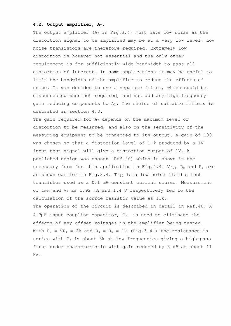
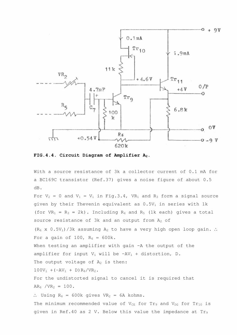
4.2. Output amplifier, A2.
The output amplifier (A2 in Fig.3.4) must have low noise as the
distortion signal to be amplified may be at a very low level. Low
noise transistors are therefore required. Extremely low
distortion is however not essential and the only other
requirement is for sufficiently wide bandwidth to pass all
distortion of interest. In some applications it may be useful to
limit the bandwidth of the amplifier to reduce the effects of
noise. It was decided to use a separate filter, which could be
disconnected when not required, and not add any high frequency
gain reducing components to A2. The choice of suitable filters is
described in section 4.3.
The gain required for A2 depends on the maximum level of
distortion to be measured, and also on the sensitivity of the
measuring equipment to be connected to its output. A gain of 100
was chosen so that a distortion level of 1 % produced by a 1V
input test signal will give a distortion output of 1V. A
published design was chosen (Ref.40) which is shown in the
necessary form for this application in Fig.4.4. Vr2, R5 and R6 are
as shown earlier in Fig.3.4. Tr10 is a low noise field effect
transistor used as a 0.1 mA constant current source. Measurement
of IDSS and VP as 1.92 mA and 1.4 V respectively led to the
calculation of the source resistor value as 11k.
The operation of the circuit is described in detail in Ref.40. A
4.7µF input coupling capacitor, C7, is used to eliminate the
effects of any offset voltages in the amplifier being tested.
With R3 = VR1 = 2k and R4 = R5 = 1k (Fig.3.4.) the resistance in
series with C7 is about 3k at low frequencies giving a high-pass
first order characteristic with gain reduced by 3 dB at about 11
Hz.
Page 50
FIG.4.4. Circuit Diagram of Amplifier A2.
With a source resistance of 3k a collector current of 0.1 mA for
a BC169C transistor (Ref.37) gives a noise figure of about 0.5
dB.
For V2 = 0 and V1 = Vi in Fig.3.4, VR1 and R3 form a signal source
given by their Thevenin equivalent as 0.5Vi in series with 1k
(for VR1 = R3 = 2k). Including R4 and R5 (1k each) gives a total
source resistance of 3k and an output from A2 of
(R6 x 0.5Vi)/3k assuming A2 to have a very high open loop gain. ∴
For a gain of 100, R6 = 600k.
When testing an amplifier with gain -A the output of the
amplifier for input Vi will be -AVi + distortion, D.
The output voltage of A2 is then:
100Vi +(-AVi + D)R6/VR2.
For the undistorted signal to cancel it is required that
AR6 /VR2 = 100.
∴ Using R6 = 600k gives VR2 = 6A kohms.
The minimum recommended value of VCE for Tr9 and VDG for Tr10 is
given in Ref.40 as 2 V. Below this value the impedance at Tr9
Page 51
collector falls significantly and consequently the open loop gain
also falls. The values of VCE and VDG are about 4.6 V and 4.4 V
respectively giving a maximum recommended peak output voltage of
about +/- 2.4 V.
The base to collector capacitance of Tr9 is effectively in
parallel with the 620k feedback resistor. The value
Of CCB is about 5 pF at VCE = 4.6 V for the BC169 transistor
used for Tr9. (Ref.37) This gives a closed loop -3dB frequency
of approximately 50 kHz.
4.3. Optional Filter Stage.
The design of simple high and low pass filters is described in
Ref.41. A variety of response shapes are possible but the most
useful in this application are the Bessel (maximally flat time
delay) and the Butterworth (maximally flat attenuation). The
Butterworth type should be used when the relative amplitudes of
distortion components in the pass band are to be preserved, e.g.
when the total output of the instrument is to be measured using a
r.m.s. reading meter. The Bessel response is more suitable when
the distortion waveform is to be displayed on an oscilloscope as
the alteration to the shape of the waveform is minimised.
Suitable filters are the active filter modules made by Barr &
Stroud Ltd. Their Series EF10/20 filters offer a choice of
Bessel, Butterworth or Chebyschev (equal ripple in the pass band
gain) and second, third or fourth order responses determined by
externally added resistors and capacitors. The range of high and
low pass -3dB frequencies is from 1 Hz to 30 kHz with a maximum
input signal of 5 V peak.
4.4. Total Circuit Noise.
A resistance of R ohms at temperature T°K generates thermal noise
of r.m.s. value (4kTRB)1/2 volts where k is Boltzmann's constant
(1.38 x 1O-23 joules / °C) and B is the noise bandwidth in Hz.
At T = 300°K and B = 20 kHz the r.m.s. noise voltage,
Page 52
Vn = 0.58 R1/2 µV (For R in kohms)
∴ 2k gives Vn = 0.82 µV,
The thermal noise voltages in the complete circuit of the test
instrument are shown in Fig.4.5.
FIG.4.5. Thermal noise Voltages in the Test Circuit.
(A is the voltage gain of the amplifier being tested).
Vn1 and Vn2 are added by A1 and appear in series with R3 and
therefore add to Vn3. The addition of r.m.s. voltages Vn1, Vn2 and
Vn3 gives a total of (Vn12 + Vn22 + Vn32)1/2 = 1.4 µV.
The Thevenin equivalent of R3 and VR1 gives the sum of noise
voltages (1.4 / 2) µV and (0.82 / 2) µV in series with 1k. The
addition of Vn5 gives a total of 1.1 µV in series with 3k.
The noise voltages added by A2 give output noise voltages of
about:
(1.1 x 600)/3 µV from the input stage,
(1.4 x A1/2 x 600)/6A µV from VR2,
(14 x 600)/600 µV from R6.
Generally A>=1. The greatest contribution from Vn6 is for the
minimum value of A. Therefore for a worst case output noise
voltage put A = 1.
The noise voltages to add are then 220 µV, 140 µV and 14µV. The
Page 53
total output noise voltage is then 260 uV.
For a test signal of 1 V a distortion signal of 2.6 µV
representing 0.00026 % distortion will be multiplied by 100 to
give 260 µV output from A2. Therefore the distortion signal will
fall below the level of the thermal noise voltage at distortion
levels of less than about 0.00026 % with a 1V test signal. This
does not however represent a lower limit of t.h.d. or i.m.d.
measurement possible as the individual components of a distortion
signal can be extracted from the wide band noise by the use of a
wave analyser as explained in section 1.2, page 6.
The noise generated by the amplifier being tested may he more
significant than that of the test circuit. If not then an
increase in distortion to noise ratio can be gained by placing an
attenuator at the input of the amplifier being tested and using
the larger amplitude signal at the input of the attenuator for
comparison in the test instrument. For an attenuation 1/K at the
amplifier input the test signal must be increased by a factor K
and therefore the maximum amplitude of test signal may then be
limited by the maximum signal which the unity gain inverting
amplifier, A1, can handle without introducing significant
distortion.
Page 54
CHAPTER 5.
PRACTICAL EVALUATION OF THE MEASURING CIRCUIT.
A series of measurements were made to investigate the practical
abilities and limitations of the test circuit developed in
Chapter 4.
Apparatus used.
Signal generator: Farnel type ESG1.
Oscilloscope: Telequipment D67 dual trace.
Oscilloscope camera: Telford type A, with Polaroid 107C Film.
Stabilised power supply: Weir Minoreg type 325 (for 741 op-amp
supply).
Batteries type PP6 9 volt (for instrument supply).
Dymar A.F. Wave Analyser Type 1771.
Resistors used in test instrument (R1, R2, R3, R4, R5 VR1 and VR2
in Fig.3.4): 0.5 W metal oxide from RS Components Ltd.
Op-amp type ML741CS.
Resistance box.
Procedure.
The measuring instrument was built using the circuit described
in Chapter 4. For most of the measurements to be described an
additional amplification stage was used to increase the output
to a sufficient level for display on the oscilloscope which has
a maximum sensitivity of 10 mV/cm. This amplifier stage is shown
In Fig.5.1. The gain provided is - 10 giving a total instrument
gain of 60 dB. The -3 dB frequency range of the stage is about
15 Hz to 100 kHz.
Fig.5.1. Additional Gain Stage.
Page 55
The following measurements were made:
5.1. Frequency Response of the Instrument.
The frequency response of the test instrument was measured by
applying a sine wave input signal of 10 mV peak amplitude across
the differential input (with VC1 = VC2 = 0) and observing the
output of amplifier A2 on the oscilloscope. The gain at 1 kHz
was found to be close to 100 when the feedback resistor, R6, was
chosen as 680k. The gain relative to that at 1 kHz is shown for
a range of frequencies in Table 5.1.
Table 5.1. Frequency response of instrument.
Frequency Gain relative to 1 kHz.
20 kHz - 0.45 dB
30 kHz - 0.92 dB
40 kHz - 1.4 dB
50 kHz - 1.9 dB
60 kHz - 2.5 dB
70 kHz - 3.1 dB
80 kHz - 4.1 dB
90 kHz - 4.8 dB
100 kHz - 5.2 dB
5.2. Distortion of the Instrument.
The instrument distortion can be measured using a common mode
input signal as described in Section 4.1.5. The distortion of
the signal generator was first measured using the Dymar wave
analyzer.
At an output of 1V r.m.s. at 2kHz the distortion at the
individual harmonic frequencies is shown in Table 5.2.
Table 5.2. Distortion of the signal generator at 2kHz
Page 56
Frequency of
harmonic.
Amplitude relative
to fundamental
4 kHz 0.48 % (-46 dB)
6 kHz 0.13 % (- 58 dB)
8 kHz 0.037 % (- 69 dB)
10 kHz 0,028 % (- 71 dB)
The higher harmonics could not be measured as they were below
the noise level of about 0.01 % (-80 dB).
(The manufacturer’s specifications state that the wave analyser
can make measurements down to - 74 dB.)
At an output of 1V r.m.s. at 20 kHz the distortion at the second
harmonic frequency of 40 kHz was 0.47 % (-47 dB).
The wave analyser has a maximum frequency of 50 kHz so the
higher order harmonics could not be measured.
Applying a 2kHz common mode signal of peak amplitude 1V to the
differential input of the instrument the fundamental output was
reduced by adjustment of VC3 (Fig.4.1) and VR1 (Fig.3.4). For VR1
a network of fixed resistors and a potentiometer were used as
described in section 3.5. The network used in this case is shown
in Fig.5.2.
FIG.5.2. Network used for VR1.
The capacitor used for VC3 was of the Philips "beehive"
Page 57
air-spaced trimmer type, of maximum value 8 pF in parallel with
a fixed capacitor of value 5.6 pF.
The output of the instrument (overall gain 60 dB) at 2 kHz was
reduced to about -51 dB relative to the input signal (measured
with the wave analyser) giving a common mode rejection ratio
(CMRR) of 111dB at 2kHz. This is only a typical value as the
ratio changed slowly with time.
With no further adjustments to VR1 or VC3 the CMRR was measured
at higher frequencies giving results in Table 5.3.
Table 5.3. CMRR with value optimized at 2 kHz.
Frequency CMRR
2 kHz 111 dB
4 kHz 106 dB
6 kHz 104 dB
8 kHz 103 dB
10 kHz 102 dB
20 kHz 99 dB
VC3 and VR1 were adjusted with an input of 20kHz to optimise the
value of CMRR at this frequency. The CMRR then became 110 dB.
With the same settings of VC3 and VR1 the CMRR at 40 kHz was
found to be 92 dB.
From the values of CMRR the effect of the generator distortion
can be calculated when measuring the distortion of the
instrument at 2 kHz or 20 kHz. For a common mode input signal of
2 kHz with distortion dn at the nth harmonic and CMRR Cn at the
harmonic frequency (Cn and dn in dB) the effect of the generator
distortion will be identical to that of dn - Cn (in dB)
distortion generated by the amplifier A1 at the nth harmonic
relative to the common mode input signal.
Page 58
For CMRR optimised at 2 kHz the distortion level in A1 which
would give the same instrument output as the common mode
generator distortion is given in Table 5.4.
Table 5.4. Effect of generator distortion
Frequency Equivalent A1 distortion
4 kHz - 46 –106 = - 153 dB
6 kHz - 58 –104 = - 162 dB
8 KHz - 69 -103 = - 172 dB
10 kHz - 71 –102 = - 173 dBB
Similarly for CMRR optimised at 20 kHz the second harmonic
generator distortion will give the same instrument output
amplitude at 40 kHz as second harmonic distortion in A1 of
(- 47 - 92) dB = - 139 dB.
These figures give the limit of measurement of distortion of A1
when using the signal generator tested. The distortion of the
later stages of the instrument is not likely to be significant
as only the distortion and the common mode breakthrough will be
distorted and these are all at very low levels.
The harmonic distortion was measured using a 2 kHz common mode
signal with CMRR optimised at that frequency. The distortion
levels measured at the harmonics are shown in Table 5.5.
Table 5.5. A1 Distortion, 2kHz input.
Frequency Amplitude relative to the
fundamental
4 kHz
6 kHz
8 kHz
-140 to - 146 dB
- 141 to - 144 dB
Not measurable
Similarly at 20 kHz the second harmonic distortion (40 kHz) was
Page 59
measured as - 118 dB (including a correction for the fall in
gain of the instrument at 40 kHz from Table 5.1).
The distortion figures are all well within the limits set by the
generator distortion breakthrough. The figures for 2 kHz signal
distortion are, however, very approximate as the distortion is
of the same order of magnitude as the noise detected by the wave
analyser and the readings fluctuated considerably. Only the
second and third harmonics were of sufficient amplitude to be
distinguishable from noise when displaying the wave analyser
output on an oscilloscope (with its timebase triggered by the
signal generator output).
At lower test signal amplitudes the distortion reduced as
expected and became unmeasurably low at all harmonics. At higher
amplitudes the distortion remained very low up to about 4.5 V
common mode signal beyond which it rose rapidly.
Adjustment of the input stage current source FET (Fig.4.1) gave
no significant change in the second harmonic distortion
indicating that the input stage contribution to this must be
small.
5.3. Measurement on a 741 op-amp.
A 741 op-amp (type ML741CS) was used in the circuit arrangement
shown in Fig.5.3 to demonstrate both the effectiveness of the
load compensation arrangement (Section 3.4.) and the ability of
the test instrument to extract low level distortion wave forms.
Page 60
Fig.5.5. Circuit of 741 Amplifier Used in Tests.
V1, V2, V5, V6 and V7 are as shown in Figs 3.4 and 3.6, which also
shows the connections to the test instrument. The 82ohm output
resistor is included to increase the effect of the load on the
output signal and thereby make the test more demanding.
The phase compensation components VC1 and VC2 (Fig.3.4) were in
this case each a 15OpF fixed capacitor in parallel with a 56 pF
trimmer capacitor.
With no load connected VR1, VC1 and VC2 were adjusted in an
attempt to cancel out the fundamental for test frequencies of
2kHz and 20kHz but it was found that when adjusted at 2kHz for
optimum cancellation an extra phase lag was always required in
the phase compensation network for optimum cancellation at
2OkHz. The best results were obtained with VC1 and VC2
approximately equal. This gives the maximum effective time delay
as shown in Section 3.1. With optimum adjustment at 2 kHz the
fundamental breakthrough at 20kHz vas observed on the
oscilloscope and seen to be of the same order of magnitude as
the distortion produced by that frequency.
The networks used for VR2 and VR3 in this case are as shown in
Fig.5.4. The 250pF variable capacitor, VC4, was a compression
type trimmer used to compensate for high frequency phase errors.
Page 61
FIG.5.4. Networks Used For VR2 and VR3.
Measuring the output of the test instrument with the wave
analyser the rejection of a 2kHz test signal was optimised using
VR2, VC1 and VC2. The values of VC1 and VC2 were estimated as
170pF each after adjustment. A 1 V peak amplitude test signal
was used for all the tests on the 741 op-amp. The instrument
output at 2kHz was reduced to - 53 dB relative to the test
signal input. Taking into account the 60 dB gain of the
instrument the rejection of the 2kHz signal is - 113 dB. With
the same component settings the signal rejection was measured at
higher frequencies and the results are shown in Table 5.6.
Page 62
Table 5.6.Best Obtainable Rejection of Signals with Rejection
optimized at 2 kHz.
Frequency Rejection
2 kHz - 113 dB
4 kHz - 104 dB
6 kHz - 94 dB
8 kHz - 87 dB
10 kHz - 83 dB
20 kHz - 71 dB
Increasing one of the phase compensation capacitors VC1 or VC2
improved the rejection at 2OkHz to -90 dB. With this setting the
rejection at an input frequency of 4OkHz was found to be - 58dB.
These results can be combined with the measured values of
generator distortion to calculate the limit to distortion
measurements set by generator distortion breakthrough. The
limits calculated are shown in Table 5.7 for a 2kHz test
frequency.
Table 5.7. Limit of Distortion Measurement with 2kHz signal.
Frequency Limit to measurement due to
generator distortion
4 kHz (-46 -104)dB = - 150dB
6 kHz (-58 - 94)dB = - 152dB
8 kHz (-69 - 87)dB = - 156dB
10 kHz (-71 - 83)dB = - 154dB
For a 20kHz test frequency the limit to second harmonic
distortion measurement is (-47-58) dB = -105 dB.
The distortion waveform obtained at the test instrument output
at a test frequency of 2 kHz was photographed and is shown in
Fig.5.5.
Page 63
FIG.5.5. Upper: Test signal, 2V p-p, 2 kHz.(1 V/ div.)
Lower: Distortion waveform, no load, 28 µV p-p.(20 µV/ div.)
Peak distortion: O.OO14 % - 97 dB)
No load was connected but it should be noted that the test
instrument has an input impedance of about 6k which may have a
significant effect on the 741 amplifier distortion.
A 1 kohm load was then connected in the position shown in
Fig.5.3 and the load effect compensation components VR3 and VC4
adjusted to cancel the 2 kHz fundamental. The distortion
waveform then obtained is shown in Fig.5.6.
FIG.5.6. Upper: Test signal, 2V p-p. 2 KHz. (1V/ div.)
Lower: Distortion waveform, 1 kohm load, 48 µV p-p,
(20 µV/ div.)
Peak distortion: 0.0024 % (- 92 dB).
Page 64
The peak to peak amplitudes of test signal and distortion
waveforms were compared to give a total peak distortion figure.
The distortion waveforms contain significant noise components
and the peak to peak distortion values used are therefore only
estimates attempting to neglect the noise. With the 2 kHz test
signal the total peak distortion is found to be:
No load, 0.0014 % (- 97 dB).
1k load, 0.0024 % (- 92 dB).
The measurement procedure was repeated at a test signal
frequency of 20 kHz. The result with no load is shown in Fig.5.7
and with a 1k load in Fig.5.8. The peak distortion levels are:
No load, 0.03 % (- 70 dB).
1k load, 0.04 % (- 68 dB).
Both can be seen to be predominantly second harmonic.
The values for both 2 kHz and 20 kHz are well within the limits
set by signal generator distortion breakthrough.
FIG.5.7. Upper: Test signal, 2V p-p, 20 kHz.(1V/ div.)
Lower: Distortion waveform, no load, 0.6 mV (O.5 mV/ div.)
Peak distortion: 0.03 % (- 70 dB).
Page 65
FIG.5.8. Upper: Test signal, 2V p-p, 20 kHz.(1V/ div.)
Lower: Distortion waveform. 1 kohm load, 0.8mV p-p (0.5mV/ div.)
Peak distortion: 0.04 % (- 68 dB).
To demonstrate the ability of the load compensation circuit
arrangement to eliminate the effects of loads with reactive and
non-linear components the load shown in Fig.5.9 was used.
FIG.5.9. Load with resistive, reactive and non-linear
components.
The circuit was first adjusted with a test signal of 2 KHz
giving an output with no load connected similar to that shown
previously in Fig.5.5. On connecting the load (Fig.5.9) with the
load compensation components VR3 and VC4 disconnected the test
instrument output waveform became as shown in Fig.5.10. I.e. The
waveform peak to peak amplitude increased by a factor of about
Page 66
1000. The extra gain stage (Fig.5.1) was not used for Fig.5.10.
FIG.5.10. Upper: Test signal, 2V p-p, 2 kHz. (1V/div.)
Lower: Distortion, Fig.5.9 load, 26mV p-p, (10 mV/div.)
Peak distortion: 1.3 % (- 38 dB).
Connecting VR3 and VC4 and adjusting them for minimum total peak
distortion gave the result shown in Fig.5.11.
FIG.5.11. Upper: Test signal, 2 V p-p, 2 kHz, (1V/ div.)
Lower: Distortion, Fig.5.9 load compensated,
40 µV p-p, (20 µV/ div.)
Peak distortion: 0.0020 % (- 94 dB).
The distortion waveforms of Figs 5.5 to 5.8 and 5.11 were
analysed using the wave analyser and the results are presented
in Table 5.8.
Page 67
Table 5.8. Wave analyser measurements of the distortion.
Fundamental: 2 kHz 2 kHz 20 kHz 20 kHz 2 kHz
load : None 1k None 1k Fig.5.9
Harmonic no. dB dB dB dB dB
2 -96 -91 -71 -69 -94
3 -100 -111
4 -109 -111
5 -115 -115
6 -119 -119
7 -129
The higher order distortion components not shown in the table
for the 2 kHz test signal were all below the noise level.
The Dymer A.F. Wave Analyser Type 1771 used to measure the
amplitudes of the harmonics has the following specifications:
Frequency range: 20 Hz to 50 kHz.
Selectivity: -3 dB ± 5 Hz.
- 40 dB ± 50 Hz.
- 60 dB ± 100 Hz.
- 70 dB ± 200 Hz.
Residual noise < - 80 dB.
i.m.d. < - 70 dB.
Page 68
CHAPTER 6.
MEASUREMENTS OF POWER AMPLIFIER DISTORTION.
6.1. Power Amplifier Design.
To illustrate some of the uses of the test instrument in the
testing of power amplifiers an amplifier was designed and built.
The circuit is shown in Fig.6.1 and is the usual arrangement of
differential input stage, driver, and class-B output stage.
An additional common collector stage Tr3, is included. This gives
the driver stage, Tr4, a low source impedance and consequently
reduces distortion caused by the Early effect. It also reduces the
effect of feedback from collector to base via CCB giving a wider
bandwidth. The use of this technique is a suitable alternative to
the cascode arrangement used earlier (Amplifier A1, Fig.4.1)
having the advantage that the available output voltage swing is
not reduced. Tr5 and Tr6 form a temperature dependent current
source. The collector current of Tr6 is proportional to the base
to emitter voltage of Tr5, which has the same temperature
coefficient as the base to emitter voltages of the output stage
transistors. By placing Tr5 in thermal contact with the output
transistor heat sink the effect on the quiescent current of
temperature changes caused by output stage power dissipation can
be partly compensated for, although there will be a delay in the
compensation due to the thermal time constants involved. The
output stage quiescent current produced can be set to the required
value by VR4. Tr7 and Tr8_ are shown as single transistors but are
actually Darlington pairs. The current gain is specified as a
minimum of 750 at IC = 3A.
Page 69
FIG.6.1. Circuit of Power Amplifier.
Page 70
As current limited power supplies were used with a maximum
current of about 0.5A a load resistance of 22 ohms was chosen
with a supply voltage of ± 15V so that an output voltage of
20V peak to peak could be used for the tests. For a sine wave
signal this represents an output power of 2.3W. While this is
not representative of the usual operating conditions with a
loudspeaker it is sufficient for the intended tests. The high
frequency stabilisation was arrived at largely by trial and
error. The use of a feedback capacitor to the base of Tr1
reduces the possibility of the occurrence of transient
intermodulation distortion (t.i.d.) (Ref.6) or slew rate
limiting as described in Ref.12.
The connections to two signal generators are shown for the
demonstration of intermodulation distortion. A low pass first
order filter is included at the input. This is required when
using square wave test signals so that their harmonics beyond
the audio frequency range can be attenuated. Using the 0.068uF
capacitor shown the -3 dB frequency of the filter is 17.5 kHz.
This was used in all the tests to be performed. The need for
such a filter when carrying out t.i.d. tests is described in
Ref.18, which suggests a higher -3 dB frequency (30 kHz). The
choice depends on the frequency range of the signals which the
amplifier is intended to handle.
The amplifier has a low frequency gain of - 10 and is direct
coupled to avoid the need for low frequency gain and phase
compensation in the test instrument. The amplifier was built
on Veroboard and the output transistors mounted on a beat sink
consisting of a 1/8" thick sheet of aluminium about 3" x 4".
The input and feedback resistors were O.5W metal oxide types
to give stable closed loop gain and low distortion.
Page 71
6.2. Test Results.
The tests carried out were to detect the presence of crossover
distortion, t.i.d, and phase modulation. As the intention is
only to illustrate some of the uses of the test instrument no
attempt has been made to analyse the distortion generating
processes within the amplifier or to obtain accurate numerical
distortion specifications. The results are presented as
photographs of the oscilloscope traces obtained together with
brief comments on the interpretation.
The instrument was adjusted to compensate for the gain and
phase response of the amplifier. No load effect compensation
was required as a resistive load was used. VR2 was a network
of fixed resistors and a potentiometer similar to those used
previously but with a total value of about 60kohms. For
optimum high frequency phase and gain compensation VC1 was
zero while VG2 was a 56 pF variable capacitor in parallel with
a total of 537 pF. When adjusted the total value of VC2 was
estimated as 580 pF.
The total peak to peak instrument output signal was measured
at a range of frequencies with the compensation adjusted for
good rejection of fundamental frequencies throughout the whole
audio frequency range. The values obtained include distortion
but give an indication of the accuracy of the compensation
obtained as at all frequencies the fundamental breakthrough
predominated. The rejection can be seen to be better than 90
dB up to 20 kHz. The results are shown in Table 6.1.
As the distortion was below the test frequency breakthrough
with this optimum wide band compensation it was found to be
necessary to adjust the compensation for best indication of
the distortion in each of the tests performed.
Table 6.1. Rejection of Fundamental With Compensation
Optimised For Wide Band Signal Use. Amplifier Output = 2OV p-
p.
Frequency Rejection, dB
100 Hz 98
500 Hz 98
Page 72
1 kHz 98
2 kHz 98
4 kHz 95
6 kHz 92
8 kHz 92
10 kHz 91
12.5 kHz 94
15 kHz 95
17.5 kHz 92
20 kHz 90
25 KHz 84
Figs. 6.2 and 6.3 show the sine wave distortion obtained at
frequencies of 2 kHz and 20 kHz respectively. The output stage
quiescent current, IQ, was adjusted for minimum peak to peak
distortion in each case and measured as 36 mA for 2 kHz and 40
mA for 20 kHz.
FIG.6.2. Upper: Amplifier output, 20V p-p, 2 kHz.
Lower: Distortion, 120 µV p-p (At amplifier 0/P).
Peak distortion: 0.0006 % (- 104 dB).
Page 73
FIG.6.3. Upper: Amplifier output, 20V p-p, 20 kHz.
Lower: Distortion, 25O µV p-p.
Peak distortion: 0.0013 % (- 96 dB). IQ = 40 mA.
Reducing IQ to 25 mA gave the result shown in Fig.6.4 (2 kHz
test signal) while increasing it to 100 mA gave Fig.6.5.
FIG.6.4. Upper: Amplifier output, 20V p-p, 2 kHz.
Lower: Distortion, 340 µV p-p.
Peak distortion: 0.0017 % (- 95 dB). Iq = 25 mA.
FIG.6.5. Upper: Amplifier output, 20 V p-p, 2 kHz.
Lower: Distortion, 340 µV p-p.
Peak distortion: 0.0017 % (- 95 dB). IQ = 100 mA.
Page 74
Note: All photographs with the exception of Figs 6.3. 6.4,
6.5, 6.6 and 6.7 (including those in Chapter 5) were obtained
with the oscilloscope in the alternate trace mode using the
single shot facility. This gives good indication of waveforms
with a high noise content but does not always give accurate
relative phase of the two traces as there is a time delay
between photographing them and the oscilloscope was found to
not always trigger on exactly the same part of the wave-form
with single shot operation. The single shot trigger control
must be pressed twice with the alternate trace mode to give
the two traces. The camera shutter is held open (exposure time
control setting "B") while the traces are triggered. Figs 6.3,
6.6 and 6.7 used a continuous trace with camera exposure time
setting no.8. Figs 6.4 and 6.5 used single shot with chop mode
dual trace to give accurate relative phase indication together
with minimised noise effect.
By feeding the amplifier output into the external timebase
input of the oscilloscope and the test instrument output into
the usual vertical input, traces similar to those described in
Chapter 2 can be obtained. The test and distortion signals of
Figs 6.2 and 6.4 were used to show the effect of reducing IQ
below its optimum value at 2 kHz. The results are shown in
Figs 6.6 and 6.7 for optimum and reduced IQ respectively.
FIG.6.6. Horizontal: Amplifier output, 2OV p-p, 2 kHz
Vertical: Distortion, 120 µV p-p.
(Signals used are as in Fig.6.2). IQ = 36 mA
Page 75
FIG.6.7. Horizontal: Amplifier output, 20V p-p, 2 kHz
Vertical: Distortion, 340 µV p-p.
(Signals used are as in Fig.6.4).
IQ = 25 mA.
Attempts to produce single line traces (i.e. traces without
loops) by adjustment of phase shifts were not successful.
In an attempt to detect t.i.d. a square wave and sine wave
were added at the amplifier input. Adjustment of the
compensation components to cancel the 15 kHz sine wave used
gave Fig.6.8.
FIG.6.8. Upper: Square wave, 16V p-p, 1.5 kHz,
plus sine wave, 2V p-p, 15 kHz. (Amplifier output).
Lower: Test instrument output, equivalent to
amplifier output distortion of 1 mV/ div.
Page 76
To find whether any intermodulation was taking place the
instrument output with the square wave alone applied to the
amplifier was observed and is shown in fig.6.9.
FIG.6.9. Upper: Square wave, 16V p-p, 1.5 kHz.
Lower: Test instrument output as for Fig.6.8.
The two distortion traces appear to be only the sum of the
individual distortion components, suggesting that t.i.d. is
not significant in this amplifier. It has been shown (Ref.6)
that t.i.d. is caused by the overshoot in the input stage
closed loop input signal resulting from the square wave
component of the test signal. This overshoot occurs unless the
open loop voltage gain - 3 dB frequency is greater than or
equal to the - 3 dB frequency of a low pass first order filter
through which the square wave has first been passed. The
relevant open loop voltage gain figure is that measured from
the input transistor base to the amplifier output in the case
of a shunt feedback design. In the circuit of Fig.6.1 the open
loop gain is reduced by the 3300 pF high frequency
compensation capacitor in parallel with 5.6k giving a - 3 dB
frequency of 8.6 kHz which is less than the 17.5 kHz low pass
filter -3 dB frequency used, t.i.d. should therefore occur,
but is not necessarily significant provided the input stage
can handle the overshoot without becoming excessively non-
linear. The overshoot can be observed by amplifying and
displaying the waveform at the input transistor base with the
square wave test signal input applied to the amplifier in the
closed loop condition. This was done using the test instrument
Page 77
as a high gain low noise amplifier and the result is shown in
Fig.6.10 in which the overshoot is clearly visible.
FIG.6.10.
Upper: Square wave amplifier output, 16V p-p, 1.5 kHz.
Lower: Tr1 (Fig.6.1) base voltage, 200 µV/div.
Overshoot: 460 uV amplitude.
Steady state: 210 uV amplitude.
Percentage overshoot: 120 %
The result may have been affected significantly by the loading
due to the test instrument and a high input impedance buffer
stage should ideally be used for such tests.
Finally the traces shown in Figs 6.11 and 6.12 were obtained
to illustrate the detection of phase modulation. 2 kHz and
20 kHz signals were used and the phase modulation caused by
the 2 kHz signal is indicated by the rise in the 20 kHz
component of the distortion waveform at certain parts of the
2 kHz wave. Adjustment of the phase compensation capacitor VC2
(Fig.3.4) moved the position of the maximum 20 kHz
breakthrough from the position shown in Fig.6.11 to that in
Fig.6.12.
Adjustment of the gain by VR2 could not move the position to
this extent and this suggests that the observation is
primarily of phase rather than amplitude modulation.
Page 78
FIG.6.11. Upper: Amplifier output, sum of 2 kHz and 20 kHz
sine waves, each 10V p-p.
Lower: Test instrument output, equivalent to amplifier output
distortion of 1 mV/ div.
FIG.6.12. As for Fig.6.11 but with phase compensation capacitor
(VC2) readjusted.
Page 79
CONCLUSIONS.
The measurements performed confirm that the direct comparison
method is capable of a high level of performance. The harmonic
distortion generated by the instrument developed is of the order
of -140 dB at 2 kHz and - 118 dB at 20 kHz (second harmonic) at
input signal peak amplitude of 1V when testing non-inverting
amplifiers. For the testing of inverting amplifiers the unity gain
amplifier in the instrument (A1) does not contribute significantly
to the instrument distortion and the ultimate limit of measurement
is set by the non-linearity of the passive components used,
particularly the resistors. Even using a relatively high
distortion signal generator (typically 0.5% t.h.d.) it has been
shown that the limit to measurements of harmonic distortion due to
breakthrough of harmonic distortion of the generator is not a
significant factor in typical low distortion measurements.
The second harmonic instrument distortion measured using a
common-mode input signal of 1V peak amplitude at 20 kHz is about
12 dB higher than the figure calculated in Ch.4. This suggests
that either the analysis given was not very accurate or that the
sources of distortion analysed are not the most important. The
effects of the various barrier and diffusion capacitances in the
circuit were not investigated in detail, and the non-linearity of
the metal oxide resistors used was assumed to be negligible.
There are also other effects not mentioned. E.g. the currents in
the circuit produce magnetic fields which can affect the
resistivity of a conductor in various ways. The relevant phenomena
are described in Ref.44 and include the magnetoresistance effect.
The significance of such effects is, however, difficult to
estimate. Despite the disagreement between calculated and measured
distortion values the performance of the circuit is more than
adequate for the testing of audio amplifiers.
Page 80
Using a wave analyser to analyse the test instrument output it was
shown in Ch.5 that distortion components down to about -130 dB
below the fundamental could be measured (See Table 5.8), limited
primarily by the noise from the amplifier being tested in the case
of the tests on the 741 op-amp. The use of phase detection
techniques could extend the range even further as very small
effective noise bandwidths can then he used. The range of the wave
analyser used was only about 80 dB and it can be seen therefore
that the test instrument can be used in conjunction with other
test apparatus of only moderate specifications to obtain very high
performance.
The effectiveness of the load effect cancellation arrangement
developed in Section 3.4 is demonstrated by the waveforms in Figs
5.10 and 5.11 in which the cancellation of a high level of
distortion generated by the use of a load with non-linear and
reactive components is shown. The distortion generated by the
amplifier itself is then revealed. Only a sine wave test signal
was used for this demonstration, the effectiveness when using wide
band signals depends on the accuracy with which the output
impedance of the particular amplifier to be tested can be
compensated for. Without such compensation the use of a
loudspeaker load during the testing of a power amplifier would
considerably reduce the signal cancellation possible as described
in Ref.25.
The tests carried out in Ch.6 were to illustrate some of the many
uses of the instrument. The power amplifier designed for these
tests had a very low level of distortion, which presented a severe
test of the distortion waveform extraction ability of the
instrument. The distortion waveform shown in Fig.6.2. is at a
level of - 104 dB relative to the fundamental (i.e. almost 60 dB
below the distortion level of the signal generator used) and yet
features of the waveform are clearly visible, including the second
harmonic and crossover effects. The variations of quiescent
current in the amplifier show that a reduction from the optimum
Page 81
value of about 30% gave a similar distortion amplitude to an
increase of about 180%. This demonstrates that too much quiescent
current is less serious than too little.
The traces in Figs 6.6 and 6.7 show the error voltage as a
function of amplifier output voltage as described in Ref.22. While
this in theory gives a direct indication of the non-linearity of
the transfer characteristic of the amplifier the interpretation of
the practical results may not always be easy. The separation of
the trace into two lines is generally due to phase shifts. The
changes in separation in Fig.6.6 suggest that the phase shift may
be a function of signal amplitude. The barrier and diffusion
capacitances in the amplifier can produce such an effect. The
increased separation in Fig.6.7 with reduced quiescent current may
be due to the effects of charge storage in the bases of the output
transistors (secondary crossover distortion). Further
investigation of the results of such tests would, however, be
required to learn the correct means of interpretation.
The presence of variable phase shift is confirmed by the results
given in Figs 6.11 and 6.12 in which phase modulation is
demonstrated.
The attempt to detect t.i.d. was not successful, as shown in Figs
6.8 and 6.9 where no intermodulation effects can be seen, although
such effects may be masked by the high instrument output signal
produced by the square wave. The square wave overshoot at the
amplifier input, which can be shown theoretically to occur, is
revealed by direct extraction of the input waveform as in Fig.6.9.
The overshoot amplitude is less than 0.5 mV and is therefore not
of sufficiently large value to cause significant input stage non-
linearity.
The main limitation of the instrument in practical use was found
to be the difficulties in providing accurate phase and gain
compensation to match the characteristics of the amplifier being
tested. The use of switched ranges and multi-turn controls would
Page 82
make the adjustments easier. The methods used during the
experimental evaluation were very time consuming and are not to be
recommended for more general use.
The 741 op-amp tested needed more effective time delay in the
compensation circuit than was available from the simple network
used. The use of more complex all-pass active filter circuits for
the provision of time delay could solve this problem if required
although these would use further amplifiers which would add
distortion and may reduce the minimum levels which can be
measured.
Page 83
REFERENCES.
1. R.B.H.Becker, High-power Audio Amplifier Design,
Wireless World, February 1972, p.79,
2. S.Kelly, Loudspeaker Enclosure Survey,
Wireless World, November 1972, pp.552-558.
3. S.Curtis,(Cambridge Audio) Letter,
Wireless World, February 1976, p.41.
4. A.McKenzie, Interface 3: Amplifier to loudspeaker,
Hi-Fi News & Record Review, Jan, 1977, pp.65-69.
5. Federation of British Audio translation of the Deutscher
Industrie Normenausschuss, 1966 DIN 45 500.
6. D.G.Daugherty and R.A.Greiner, Some Design Objectives for
Audio Power Amplifiers,
IEEE Transactions on Audio and Electroacoustics Vol.AU-14,
No.1, March 1966, pp.43-48.
7. J.P.Stuart, An Approach to Audio Amplifier Design,
Part 3, Wireless World, Oct.1973, pp.491-494.
8. E.R.Wigan, New Distortion Criteria,
Electronics Technology, April 1961, p.126.
9. W.Colloms, What Has Gone Wrong With Amplifier Evaluation?
Hi-Fi News & Record Review, Oct.1977, pp.83-85.
10. P.J.Baxandall, Audible Amplifier Distortion Is Not
A Mystery, Wireless World, Nov.1977, pp.65-66,
11. Letters, Audible Amplifier Distortion,
Wireless World, Jan.1979, pp.43-45.
12. Various letters and articles,
Hi-Fi News & Record Review, Jan.1978, pp.75-83.
13. Letters, Audible Amplifier Distortion,
Wireless World, Feb.1978, p.54.
14. Letters, Amplifier Claims (Reply from Radford Audio
Ltd,), Wireless World, Jan.1975, p.20.
15. M.Otala, Non-Linear Distortion In Audio Amplifiers,
Wireless World, Jan.1977, pp,41-43.
Page 84
16. Data given by Radford laboratory Instruments Ltd.,
Bristol BS3 2HZ on the Radford Series 3 Distortion Measuring
Set.
17. Data given by Marconi Instruments Ltd., Longacres,
St.Albans, Hertfordshire.
18. E.Leinonen, M.Otala, J.Curl, A Method For Measuring
Transient Intermodulation Distortion (TIM), JAES, April
1977, Vol.25, No.4, pp.170-177.
19. IEEE Proposed Standard For Measurement Of Loudspeaker
Electrical Impedance,
IEEE Transactions on Audio and Electroacoustics, June 1970,
pp.213-217. Part 3, Section 3.1, "Acoustic Environment".
20. R.A.Belcher, An Experimental Investigation of Test-Noise
Signals For The Measurement Of Non-Linear
Distortion of Sound Signals, BBC Research Department Report
No.1974/2.
21. R.A.Belcher, A Comb Filter Method For Measuring
Distortion, BBC Research Department Report No. R.D. 1976/12
REFERENCES 22 TO 29, SEE CHAPTER 2 (LITERATURE SURVEY).
30. H.V.Bode, Relations Between Attenuation and Phase in
Feedback Amplifier Design,
Bell System Tech.J.,19,pp.421-454,July 1940.
Reprinted: Circuit Theory, pp.252-28
Ed. M.E.Van Valkenturg,
Pub. Dowden, Hutchinson and Rosa.
31. R.A.Fairs, Resistors,
Wireless World, Oct. 1975, pp.487-492.
32. Takahisa, Yanagisaw and Shiomi, Nonlinearity of
Resistors and Its Geometric Factor. Electronics and
Communications in Japan, Vol. 56-C, No.6, 1975, pp.101-107.
33. A. Sandman, Reducing Amplifier Distortion,
Wireless World, Oct.1974, pp.367-371.
Page 85
34. H.P.Walker, letter, Feedback Amplifiers,
Wireless World, April 1973, p.193.
35. T.Magchielse, letter, Series and Parallel Feedback,
Wireless World, Feb.1975, p.68.
36. E.F.Taylor, Distortion in Low Noise Amplifiers,
Part 1, Distortion Analysis, Wireless World, Aug.1977,
pp.28-32.
37. Siemens Semiconductor Manual 1970 / 1971.
pp.278-289 (BC169C) and pp.308-319 (BC259B).
38. E.F.Taylor, Distortion in Low Noise Amplifiers,
Part 2, Wireless World, Sept.1977, pp.55-59.
39. P.J.Baxandall, Audio Power Amplifier Design,
Wireless World, Jan-1978, pp.53-57.
40. J.L.Linsley Hood, The Liniac,
Wireless World, Sept.1971, P.437.
41. M.Bronzite, Simple- Active Filters,
Wireless World, March 1970, pp.117-119.
43. J.R.Stuart, An Approach to Audio Amplifier Design,
Part 2, Wireless World, Sept. 1973, pp.439-446.
43. O.Mueller, Internal Thermal Feedback in Four-Poles,
Especially in Transistors, Proc.IEEE, Vol.52, Aug,1964, pp.
924-930.
44. G.T.Meaden, Electrical Resistance of Metals, Heywood
Books, London. 1966.