3.0-3.6 GHz Wideband, over 46% Average Efficiency GaN Doherty
Power Amplifier with Frequency Dependency Compensating Circuits
Yuji Komatsuzaki1, Keigo Nakatani1, Shintaro Shinjo1, Shinichi Miwa2,
Rui Ma3, and Koji Yamanaka1
1 Information Technology R&D Center, Mitsubishi Electric Corporation,
Kamakura, Kanagawa, 247-8501, Japan 2 High Frequency and Optical Device works, Mitsubishi Electric Corporation,
Itami, Hyogo, 664-8641, Japan 3 Mitsubishi Electric Research Laboratories, Cambridge, MA 02139, USA
Abstract — A wideband GaN Doherty power amplifier
(DPA) for 4G/LTE-Advanced base stations is presented. To break the inherent narrow band limitation of conventional DPA, a frequency dependency compensating circuit and a modified λ/4 inverter incorporating package parasitic elements are proposed. Measured DPA achieves 45.9-50.2 % drain efficiency with -50 dBc ACLR at 3.0-3.6 GHz under 20 MHz LTE signal after digital pre-distortion (DPD), which is very suitable for multiband radio and carrier aggregation in 4G. The use of the wideband efficient GaN DPA can reduce the complexity and energy consumption of radio, which further helps reducing the total cost of ownership (TCO) of base stations.
Index Terms — wideband, Doherty amplifier, GaN HEMT, base station, power amplifier.
I. INTRODUCTION
Recently, wireless communication systems apply high
peak to average power ratio (PAPR) signals to cope with
crowded spectrum and faster data speed demand. RF
power amplifiers for base station require high efficiency at
a large back-off level. To efficiently amplify greater PAPR
signals (>7dB) at frequency above 3 GHz, GaN Doherty
power amplifier (DPA) is preferred over LDMOS
technology due to its unique advantages [1], [2].
Moreover, there is also an increasing demand for
expanding the bandwidth of the DPA to cover multiband
of 4G/LTE-Advanced [3]. However, the DPA is
fundamentally limited to narrow frequency range due to
the frequency dependent λ/4 inverter for load modulation.
This work proposes a 3.0-3.6 GHz wideband GaN DPA
with novel frequency dependency compensating circuit.
The proposed compensating circuit compensates
frequency dependence of the λ/4 inverter mentioned above,
and it works as an inductive or a capacitive reactance
depending on the frequency. In addition, an output
configuration absorbing both transistor’s output
capacitance (Cds) and reactance of package into a part of
the λ/4 inverter is applied. The advantages of the proposed
GaN DPA configuration are clearly demonstrated by the
outperformed performance.
II. CIRCUIT CONFIGURATION OF WIDEBAND DPA
(a)
(b)
Matching
Main
Aux
Main
Aux
Offset λ/4
Matching
Divider
•Multistage matching circuit and divider •Multistage output
matching circuit
A. Absorbing Cds and parasites of package into λ/4 inverter
B. Frequency dependence compensating circuits at Aux output
λ/4
Fig. 1. Schematics of DPAs. (a) Conventional, (b) Proposed.
Fig. 1(a) and (b) compares the schematics of a
conventional and our proposed DPA. In conventional DPA,
matching circuits are connected at output of the main
amplifier (Main) and auxiliary amplifier (Aux). The offset
lines, which adjust the phase to realize correct resistive
load modulation of a Main, are connected after the
matching circuits. On the other hand, as shown in Fig 1(b),
the proposed DPA doesn’t include matching circuits and
offset line, and the λ/4 inverter is directly connected to the
equivalent current source plane of a transistor (see A in
Fig. 1(b)). In addition, the frequency dependency
compensating circuit is applied to an output of Aux (see B
in Fig. 1(b)). In this section, the operation principles of the
two key features are shown, respectively.
A. Absorbing transistor’s Cds and reactance of package
into a part of the λ/4 inverter
The concept of absorbing device capacitance and
reactance of package into a part of the λ/4 (90 degree)
978-1-5090-3458-1/17/$31.00 © 2017 IEEE PAWR 201722
inverter is shown in Fig. 2. The goal is to mimic the same
center frequency response as the ideal λ/4 transmission
line by using transistor’s Cds, reactance of package and
additional component at outside of package. The
characteristic impedance Zc is arbitrary, and the λ/4
inverter can operate as the impedance transformer under
the conditions both saturation region and back-off region.
In most cases of the conventional DPA, the electric length
from equivalent current source plane of the transistor to
combining point of the Main and Aux is more than λ/4 (e.g.
270, 450 degree) because it includes matching circuits,
offset lines and the λ/4 inverter. Compared with the
conventional DPA, the electric length of the proposed
DPA is exactly λ/4 and it can achieve wider bandwidth
performance.
Load & Aux
FET
Package’s reactance
Inside of package
Cds
ZT, θT
Equivalent λ/4 inverter Zc, λ/4 (= 90˚) @ f0
Reactance
Fig. 2. Schematic of the λ/4 inverter absorbed transistor
output capacitance and reactance of package.
B. Frequency dependency compensating circuit
The concept of the frequency dependency compensating
circuit is shown in Fig. 3. The circuit is applied to
compensate frequency dependence of the λ/4 inverter at
output of the Main. The compensating circuit is based on a
transmission line, transistor’s Cds and reactance of package
of the Aux. The electric length from the equivalent current
source plane of the transistor in the compensating circuit is
180 × N degree (N = 1, 2, 3…), and the electric length and
characteristic impedance depend on the frequency
dependence of the λ/4 inverter.
Main
Aux
open
λ/4
θ = N×180˚
Lower: InductiveCenter: OpenHigher: Capacitive
Output
Fig. 3. Schematic of the frequency dependency compensating
circuit.
Figure 4 shows the simulated frequency response of
reflection at output terminal of DPA. The parameter is
electric length in the compensating circuit under the back-
off region, and simulations are performed under the
conditions of 180 × 0, 180 × 1 and 180 × 2 degree. The
compensating circuit works as an inductive reactance at
lower frequency, and works as a capacitive reactance at
higher frequency. In this case, the compensating circuit
with 180 × 2 degree minimizes the frequency dependency
of reflection.
N×180˚□ N=0 (0˚)○ N=1 (180˚)▽ N=2 (360˚)
High frequency
Low frequency
Capacitivecompensation
Inductivecompensation
Fig. 4. Simulated frequency response of reflection at output
terminal of DPA.
III. MEASURED RESULTS
Figure 5 shows the photo of the assembled wideband
GaN DPA with frequency dependency compensating
circuit. The DPA is fabricated with MGFS39G38L2 in
Mitsubishi Electric, which contains two GaN HEMTs
inside one package. In this work, upper one is operated as
a Main, and lower one is operated as an Aux. The input
and output circuits are fabricated with RO4350B
substrates.
78 mm
60
mm
Input
Output
Fig. 5. Photo of the assembled wideband GaN DPA with
frequency dependency compensating circuit.
Fig. 6 and 7 show the measured dynamic AM/AM and
AM/PM characteristics of the assembled wideband GaN
DPA, respectively. The measurements were performed
under the conditions of both with and without DPD, and
the frequency is 3.4 GHz. The drain voltage is 30 V. An
input signal is LTE Downlink, bandwidth of 20 MHz and
PAPR of 7.5 dB. The measured results in Fig. 6 and 7
show the improvement of AM/AM and AM/PM
characteristics by DPD demonstrating good linearizability.
23
The measured adjacent channel leakage ratio (ACLR)
and drain efficiency (DE) at 3.4 GHz are shown in Fig. 8.
The ACLR is defined by the worst case of between lower
and upper frequency part of ACLR. As shown in Fig.8, the
ACLR with DPD has improvement of 10-15 dB than that
without DPD, and the proposed GaN DPA achieved the
DE of 47.7 % with ACLR of -50 dBc.
The measured frequency sweep using the same LTE-
signal for DE and output power at ACLR of -50dBc with
DPD are shown in Fig. 9. Over the 3.0-3.6 GHz frequency
band, the proposed GaN DPA obtained the DE of 45.9-
50.2 %. The measured results of the fractional bandwidth
demonstrated the proposed GaN DPA can cover multi
bands for 4G/LTE-Advanced.
A performance comparison of wideband DPAs for LTE
bands above 3 GHz is given in Table I. The proposed GaN
DPA shows the state-of–the–art performances, and the
advantages of the proposed configuration are clearly
demonstrated.
4
6
8
10
12
14
16
18
-10 0 10 20 30 40
Gai
n (
dB
)
Input power (dBm)
W/O DPDWith DPD
Fig. 6. Measured dynamic AM/AM characteristics at 3.4GHz.
-30
-20
-10
0
10
20
30
-10 0 10 20 30 40
Ph
ase
(d
eg.
)
Input power (dBm)
W/O DPDWith DPD
Fig. 7. Measured dynamic AM/PM characteristics at 3.4GHz.
0
10
20
30
40
50
60
-70
-60
-50
-40
-30
-20
-10
20 25 30 35 40
Dra
in e
ffic
ien
cy (
%)
AC
LR (
dB
c)
Output Power (dBm)
With DPDW/O DPD
Fig. 8. Measured ACLR and DE at 3.4GHz.
33.0
33.5
34.0
34.5
35.0
35
40
45
50
55
2.9 3.1 3.3 3.5 3.7
Po
ut
(dB
m)
Dra
in e
ffic
ien
cy (
%)
Frequency (GHz)
Drain efficiency, Pout @ ACPR = -50 dBc
Efficiency
Pout
Fig. 9. Measured frequency dependences of DE and output
power with ACLR of -50dBc with DPD.
TABLE I.
COMPARISON OF DPAS ABOVE 3GHZ LTE BANDS Ref. Year Freq. (GHz) η(%) Signal Condition
[3] 2012 3.0-3.6 38-56 CW 6dB backoff
[1] 2013 3.4-3.5 42.5 5 × 20MHz LTE, DPD ACLR=-48(dBc)
[2] 2014 3.45-3.55 56 5 × 20MHz LTE, DPD ACLR=-50(dBc)
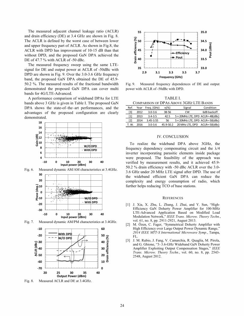
T. W. 2016 3.0-3.6 45.9-50.2 20 MHz LTE, DPD ACLR=-50(dBc)
IV. CONCLUSION
To realize the wideband DPA above 3GHz, the
frequency dependency compensating circuit and the λ/4
inverter incorporating parasitic elements inside package
were proposed. The feasibility of the approach was
verified by measurement results, and it achieved 45.9-
50.2 % drain efficiency with -50 dBc ACLR over the 3.0-
3.6 GHz under 20 MHz LTE signal after DPD. The use of
the wideband efficient GaN DPA can reduce the
complexity and energy consumption of radio, which
further helps reducing TCO of base stations.
REFERENCES
[1] J. Xia, X. Zhu, L. Zhang, J. Zhai, and Y. Sun, “High-Efficiency GaN Doherty Power Amplifier for 100-MHz LTE-Advanced Application Based on Modified Load Modulation Network,” IEEE Trans. Microw. Theory Techn., vol. 61, no. 8, pp. 2911-2921, August 2013.
[2] M. Özen, C. Fager, “Symmetrical Doherty Amplifier with High Efficiency over Large Output Power Dynamic Range,” 2014 IEEE MTT-S International Microwave Symp., Tampa, FL.
[3] J. M. Rubio, J. Fang, V. Camarchia, R. Quaglia, M. Pirola, and G. Ghione, “3–3.6-GHz Wideband GaN Doherty Power Amplifier Exploiting Output Compensation Stages,” IEEE Trans. Microw. Theory Techn., vol. 60, no. 8, pp. 2543-2548, August 2012.
24