278
DL05/06 Option Modules USER MANUAL Manual Number: D0-OPTIONS-M

DL05/06 Option Modules USER MANUAL
Manual Number: D0-OPTIONS-M

~ WARNING ~Thank you for purchasing automation equipment from AutomationDirect.com®, doing business as, AutomationDirect. We want your new automation equipment to operate safely. Anyone who installs or uses this equipment should read this publication (and any other relevant publications) before installing or operating the equipment.
To minimize the risk of potential safety problems, you should follow all applicable local and national codes that regulate the installation and operation of your equipment. These codes vary from area to area and usually change with time. It is your responsibility to determine which codes should be followed, and to verify that the equipment, installation, and operation is in compliance with the latest revision of these codes.
At a minimum, you should follow all applicable sections of the National Fire Code, National Electrical Code, and the codes of the National Electrical Manufacturer’s Association (NEMA). There may be local regulatory or government offices that can also help determine which codes and standards are necessary for safe installation and operation.
Equipment damage or serious injury to personnel can result from the failure to follow all applicable codes and standards. We do not guarantee the products described in this publication are suitable for your particular application, nor do we assume any responsibility for your product design, installation, or operation.
Our products are not fault-tolerant and are not designed, manufactured or intended for use or resale as on-line control equipment in hazardous environments requiring fail-safe performance, such as in the operation of nuclear facilities, aircraft navigation or communication systems, air traffic control, direct life support machines, or weapons systems, in which the failure of the product could lead directly to death, personal injury, or severe physical or environmental damage (“High Risk Activities”). AutomationDirect specifically disclaims any expressed or implied warranty of fitness for High Risk Activities.
For additional warranty and safety information, see the Terms and Conditions section of our catalog. If you have any questions concerning the installation or operation of this equipment, or if you need additional information, please call us at 770-844-4200.
This publication is based on information that was available at the time it was printed. At AutomationDirect we constantly strive to improve our products and services, so we reserve the right to make changes to the products and/or publications at any time without notice and without any obligation. This publication may also discuss features that may not be available in certain revisions of the product.
TrademarksThis publication may contain references to products produced and/or offered by other companies. The product and company names may be trademarked and are the sole property of their respective owners. AutomationDirect disclaims any proprietary interest in the marks and names of others.
Copyright 2018, AutomationDirect.com Incorporated All Rights Reserved
No part of this manual shall be copied, reproduced, or transmitted in any way without the prior, written consent of AutomationDirect.com Incorporated. AutomationDirect retains the exclusive rights to all information included in this document.

~ ADVERTENCIA ~Gracias por comprar equipo de automatización de Automationdirect.com®. Deseamos que su nuevo equipo de automatización opere de manera segura. Cualquier persona que instale o use este equipo debe leer esta publicación (y cualquier otra publicación pertinente) antes de instalar u operar el equipo.
Para reducir al mínimo el riesgo debido a problemas de seguridad, debe seguir todos los códigos de seguridad locales o nacionales aplicables que regulan la instalación y operación de su equipo. Estos códigos varian de área en área y usualmente cambian con el tiempo. Es su responsabilidad determinar cuales códigos deben ser seguidos y verificar que el equipo, instalación y operación estén en cumplimiento con la revisión mas reciente de estos códigos.
Como mínimo, debe seguir las secciones aplicables del Código Nacional de Incendio, Código Nacional Eléctrico, y los códigos de (NEMA) la Asociación Nacional de Fabricantes Eléctricos de USA. Puede haber oficinas de normas locales o del gobierno que pueden ayudar a determinar cuales códigos y normas son necesarios para una instalación y operación segura.
Si no se siguen todos los códigos y normas aplicables, puede resultar en daños al equipo o lesiones serias a personas. No garantizamos los productos descritos en esta publicación para ser adecuados para su aplicación en particular, ni asumimos ninguna responsabilidad por el diseño de su producto, la instalación u operación.
Nuestros productos no son tolerantes a fallas y no han sido diseñados, fabricados o intencionados para uso o reventa como equipo de control en línea en ambientes peligrosos que requieren una ejecución sin fallas, tales como operación en instalaciones nucleares, sistemas de navegación aérea, o de comunicación, control de tráfico aéreo, máquinas de soporte de vida o sistemas de armamentos en las cuales la falla del producto puede resultar directamente en muerte, heridas personales, o daños físicos o ambientales severos (“Actividades de Alto Riesgo”). Automationdirect.com específicamente rechaza cualquier garantía ya sea expresada o implicada para actividades de alto riesgo. Para información adicional acerca de garantía e información de seguridad, vea la sección de Términos y Condiciones de nuestro catálogo. Si tiene alguna pregunta sobre instalación u operación de este equipo, o si necesita información adicional, por favor llámenos al número 770-844-4200 en Estados Unidos. Esta publicación está basada en la información disponible al momento de impresión. En Automationdirect.com nos esforzamos constantemente para mejorar nuestros productos y servicios, así que nos reservamos el derecho de hacer cambios al producto y/o a las publicaciones en cualquier momento sin notificación y sin ninguna obligación. Esta publicación también puede discutir características que no estén disponibles en ciertas revisiones del producto.
Marcas RegistradasEsta publicación puede contener referencias a productos producidos y/u ofrecidos por otras compañías. Los nombres de las compañías y productos pueden tener marcas registradas y son propiedad única de sus respectivos dueños. Automationdirect.com, renuncia cualquier interés propietario en las marcas y nombres de otros.
PROPIEDAD LITERARIA 2018, AUTOMATIONDIRECT.COM® INCORPORATEDTodos los derechos reservados
No se permite copiar, reproducir, o transmitir de ninguna forma ninguna parte de este manual sin previo consentimiento por escrito de Automationdirect.com® Incorprated. Automationdirect.com retiene los derechos exclusivos a toda la información incluida en este documento. Los usuarios de este equipo pueden copiar este documento solamente para instalar, configurar y mantener el equipo correspondiente. También las instituciones de enseñanza pueden usar este manual para propósitos educativos.

~ AVERTISSEMENT ~Nous vous remercions d’avoir acheté l’équipement d’automatisation de Automationdirect.comMC, en faisant des affaires comme, AutomationDirect. Nous tenons à ce que votre nouvel équipement d’automatisation fonctionne en toute sécurité. Toute personne qui installe ou utilise cet équipement doit lire la présente publication (et toutes les autres publications pertinentes) avant de l’installer ou de l’utiliser.
Afin de réduire au minimum le risque d’éventuels problèmes de sécurité, vous devez respecter tous les codes locaux et nationaux applicables régissant l’installation et le fonctionnement de votre équipement. Ces codes diffèrent d’une région à l’autre et, habituellement, évoluent au fil du temps. Il vous incombe de déterminer les codes à respecter et de vous assurer que l’équipement, l’installation et le fonctionnement sont conformes aux exigences de la version la plus récente de ces codes.
Vous devez, à tout le moins, respecter toutes les sections applicables du Code national de prévention des incendies, du Code national de l’électricité et des codes de la National Electrical Manufacturer’s Association (NEMA). Des organismes de réglementation ou des services gouvernementaux locaux peuvent également vous aider à déterminer les codes ainsi que les normes à respecter pour assurer une installation et un fonctionnement sûrs.
L’omission de respecter la totalité des codes et des normes applicables peut entraîner des dommages à l’équipement ou causer de graves blessures au personnel. Nous ne garantissons pas que les produits décrits dans cette publication conviennent à votre application particulière et nous n’assumons aucune responsabilité à l’égard de la conception, de l’installation ou du fonctionnement de votre produit.
Nos produits ne sont pas insensibles aux défaillances et ne sont ni conçus ni fabriqués pour l’utilisation ou la revente en tant qu’équipement de commande en ligne dans des environnements dangereux nécessitant une sécurité absolue, par exemple, l’exploitation d’installations nucléaires, les systèmes de navigation aérienne ou de communication, le contrôle de la circulation aérienne, les équipements de survie ou les systèmes d’armes, pour lesquels la défaillance du produit peut provoquer la mort, des blessures corporelles ou de graves dommages matériels ou environnementaux («activités à risque élevé»). La société AutomationDirect nie toute garantie expresse ou implicite d’aptitude à l’emploi en ce qui a trait aux activités à risque élevé.
Pour des renseignements additionnels touchant la garantie et la sécurité, veuillez consulter la section Modalités et conditions de notre documentation. Si vous avez des questions au sujet de l’installation ou du fonctionnement de cet équipement, ou encore si vous avez besoin de renseignements supplémentaires, n’hésitez pas à nous téléphoner au 770-844-4200.
Cette publication s’appuie sur l’information qui était disponible au moment de l’impression. À la société AutomationDirect, nous nous efforçons constamment d’améliorer nos produits et services. C’est pourquoi nous nous réservons le droit d’apporter des modifications aux produits ou aux publications en tout temps, sans préavis ni quelque obligation que ce soit. La présente publication peut aussi porter sur des caractéristiques susceptibles de ne pas être offertes dans certaines versions révisées du produit.
Marques de commerceLa présente publication peut contenir des références à des produits fabriqués ou offerts par d’autres entreprises. Les désignations des produits et des entreprises peuvent être des marques de commerce et appartiennent exclusivement à leurs propriétaires respectifs. AutomationDirect nie tout intérêt dans les autres marques et désignations.
Copyright 2018, Automationdirect.com IncorporatedTous droits réservés
Nulle partie de ce manuel ne doit être copiée, reproduite ou transmise de quelque façon que ce soit sans le consentement préalable écrit de la société Automationdirect.com Incorporated. AutomationDirect conserve les droits exclusifs à l’égard de tous les renseignements contenus dans le présent document.

DL05/06 OptiOn MODuLes USER MANUAL
Please include the Manual Number and the Manual Issue, both shown below, when communicating with Technical Support regarding this publication.
Manual Number: D0-OPTIONS-M
Issue: 7th Edition, Revision D
Issue Date: 07/19
Publication HistoryIssue Date Description of Changes
Original 09/01 Original issueRev. A 12/01 Made changes to analog specifications
2nd edition 01/02 Added new chapter and minor changes to chapters3rd edition 05/02 Added wiring guidelines and new discrete module4th edition 07/02 Added DL06 micro PLC information4th edition
Rev. A 02/03 Minor changes and corrections
5th edition 05/03 Added new chapter6th edition 08/03 Added one new chapter and reference new discrete module6th edition
Rev. A 01/04 Added one new chapter
6th edition Rev. B
03/04 Added two new discrete modules, moved D0-01MC Memory Cartridge/Real Time Clock module to DL05 user manual
6th edition Rev. C 05/05 Added F0-08SIM module; minor corrections
7th edition 05/07 Added six new chapters for high resolution analog modules7th edition
Rev. A 08/11 Made corrections in ch 3, ch 4 and ch 6.
7th edition Rev. B 03/18 General update, made corrections to Ch 2, Ch 4.
7th edition Rev. C 03/19 Added Special Relay tables to Ch 11.
7th edition Rev. D 07/19 Updated thermocouple graphic Ch15, page 4.

Table of ConTenTs
Chapter 1 - Getting StartedIntroduction ...............................................................................................................1–2
The Purpose of this Manual ......................................................................................1–2Supplemental Manuals .............................................................................................1–2Technical Support ....................................................................................................1–2
Conventions Used ......................................................................................................1–2Key Topics for Each Chapter .....................................................................................1–2
Selecting the Proper Module ....................................................................................1–3DL05 ........................................................................................................................1–3DL06 ........................................................................................................................1–3Module Choices .......................................................................................................1–3Module Choices, continued......................................................................................1–4
Installing the Option Modules ..................................................................................1–5Remove the Slot Cover .............................................................................................1–5Insert the Module .....................................................................................................1–5
Module LED Indicator ................................................................................................1–6
Power Budgeting .......................................................................................................1–6Power supplied .......................................................................................................1–6Power required by base unit ...................................................................................1–6Power required by option cards ..............................................................................1–6
Chapter 2 - Discrete I/O GuidelinesSafety Guidelines .......................................................................................................2–2
Plan for Safety ..........................................................................................................2–2Three Levels of Protection ........................................................................................2–3Emergency Stops ......................................................................................................2–3

DL05/06 Option Modules User Manual; 7th Ed. Rev. Dii
Table of Contents
Emergency Power Disconnect ..................................................................................2–4Orderly System Shutdown ........................................................................................2–4Class 1, Division 2 Approval (Applies ONLY to modules used with a DL06 PLC.) ......2–4
System Wiring Strategies ..........................................................................................2–5PLC Isolation Boundaries ..........................................................................................2–5I/O “Common” Terminal Concepts ..........................................................................2–8Connecting DC I/O to Solid State Field Devices .......................................................2–9Solid State Input Sensors ..........................................................................................2–9Solid State Output Loads .........................................................................................2–9Relay Output Guidelines .........................................................................................2–11Prolonging Relay Contact Life ................................................................................2–11Surge Suppression For Inductive Loads ...................................................................2–12Prolonging Relay Contact Life ................................................................................2–13DC Input Wiring Methods ......................................................................................2–14DC Output Wiring Methods ...................................................................................2–14Firmware and Software ..........................................................................................2–14
I/O Addressing .........................................................................................................2–15Module I/O Points and Addressing for the DL05 and DL06 ....................................2–15All Discrete Modules Installed I/O Addressing Example: .........................................2–16Discrete and Analog Modules Installed I/O Addressing Example: ...........................2–16Discrete and Analog Modules Installed I/O Addressing Example: ...........................2–16
Discrete I/O General Specifications ........................................................................2–17
Glossary of Specification Terms ..............................................................................2–18
F0-08SIM 8-Point Simulator Input Module .............................................................2–19
D0-10ND3 10-Point DC Input Module ....................................................................2–20
D0-10ND3F 10-Point DC Fast Input Module ..........................................................2–21
D0-16ND3 16-Point DC Input Module ....................................................................2–22
F0-08NA-1 8-Point AC Input Module ......................................................................2–23
D0-10TD1 10-Point DC Output Module..................................................................2–24
D0-16TD1 16-Point DC Output Module..................................................................2–25
D0-10TD2 10-Point DC Output Module..................................................................2–26
D0-16TD2 16-Point DC Output Module..................................................................2–27
D0-07CDR 4-Point DC Input, 3-Point Relay Output Module ..................................2–28

DL05/06 Option Modules User Manual; 7th Ed. Rev. D iii
Table of Contents
D0-08TR 8-Point Relay Output Module ..................................................................2–29
D0-08CDD1 4-Point DC Input, 4-Point DC Output Module ...................................2–30
F0-04TRS 4-Point Relay Output Module .................................................................2–31
Chapter 3 - F0-04AD-1, 4-Channel Analog Current InputModule Specifications ...............................................................................................3–2
Setting the Module Jumper .......................................................................................3–4
Connecting and Disconnecting the Field Wiring .....................................................3–4Wiring Guidelines .....................................................................................................3–4
Wiring Diagram .........................................................................................................3–5Current Loop Transmitter Impedance .......................................................................3–5
Module Operation .....................................................................................................3–6Channel Scanning Sequence ....................................................................................3–6Analog Module Updates ...........................................................................................3–6
Special V-memory Locations .....................................................................................3–7Formatting the Module Data ....................................................................................3–7DL05 Data Formatting .............................................................................................3–7Structure of V7700 ...................................................................................................3–7Structure of V7701 ...................................................................................................3–7DL06 Data Formatting .............................................................................................3–8Setup Data Type and Number of Channels ..............................................................3–8Storage Pointer Setup ..............................................................................................3–8
Using the Pointer in Your Control Program .............................................................3–9DL05 Pointer Method ...............................................................................................3–9DL06 Pointer Method .............................................................................................3–10
Detecting Input Signal Loss ....................................................................................3–11Analog Signal Loss ..................................................................................................3–11
Scale Conversions ....................................................................................................3–11Scaling the Input Data ...........................................................................................3–11The Conversion Program ........................................................................................3–12Analog and Digital Value Conversions ....................................................................3–12
Special Relays ...........................................................................................................3–13DL05 Special Relays ................................................................................................3–13

DL05/06 Option Modules User Manual; 7th Ed. Rev. Div
Table of Contents
DL06 Special Relays ................................................................................................3–13
Module Resolution ...................................................................................................3–15Analog Data Bits .....................................................................................................3–15Resolution Details ...................................................................................................3–15
Analog Input Ladder Logic Filter ............................................................................3–16PID Loops / Filtering: ..............................................................................................3–16Smoothing the Input Signal (DL06 only): ...............................................................3–16Using Binary Data Format.......................................................................................3–16Using BCD Data Format .........................................................................................3–17
Chapter 4 - F0-08ADH-1, 8-Channel Analog Current InputModule Specifications ...............................................................................................4–2
Connecting and Disconnecting the Field Wiring .....................................................4–4Wiring Guidelines .....................................................................................................4–4
Wiring Diagram .........................................................................................................4–5Current Loop Transmitter Impedance .......................................................................4–5
Module Operation .....................................................................................................4–6Channel Scanning Sequence ....................................................................................4–6Analog Module Updates ...........................................................................................4–6
Special V-memory Locations .....................................................................................4–7Formatting the Analog Module Data ........................................................................4–7DL05 Data Formatting .............................................................................................4–7Setup Data Type and Number of Active Channels ....................................................4–7Storage Pointer Setup ..............................................................................................4–7DL06 Data Formatting .............................................................................................4–8Setup Data Type and Number of Active Channels ....................................................4–8Storage Pointer Setup ..............................................................................................4–8
Using the Pointer in Your Control Program .............................................................4–9DL05 Pointer Method Using Conventional Ladder Logic ..........................................4–9DL05 Pointer Method Using the IBox Instruction Available in DirectSOFT5 ..............4–9DL06 Pointer Method Using Conventional Ladder Logic ........................................4–10DL06 Pointer Method Using the IBox Instruction Available in DirectSOFT6 ............4–11

DL05/06 Option Modules User Manual; 7th Ed. Rev. D v
Table of Contents
Scale Conversions ....................................................................................................4–11Scaling the Input Data ...........................................................................................4–11The Conversion Program in Standard Ladder Logic ................................................4–12Analog and Digital Value Conversions ....................................................................4–13
Module Resolution ...................................................................................................4–14Analog Data Bits .....................................................................................................4–14Resolution Details ...................................................................................................4–14
Analog Input Ladder Logic Filter ............................................................................4–15PID Loops / Filtering ...............................................................................................4–15Smoothing the Input Signal (DL06 only) ................................................................4–15Binary Data Format Filter Using Ladder Logic ......................................................4–15BCD Data Format Filter Using Ladder Logic............................................................4–16Example Code to Scale a 4–20 mA Signal to 0–1000 BCD .....................................4–17Example Code to Scale a 4–20 mA Signal to 0–1000 Binary ..................................4–18
Chapter 5 - F0-04AD-2, 4-Channel Analog Voltage InputModule Specifications ...............................................................................................5–2
Setting the Module Jumpers .....................................................................................5–4
Connecting and Disconnecting the Field Wiring .....................................................5–5Wiring Guidelines .....................................................................................................5–5
Wiring Diagram .........................................................................................................5–5
Module Operation .....................................................................................................5–6Input Channel Update Sequence ..............................................................................5–6Analog Module Updates ...........................................................................................5–6
Special V-memory Locations .....................................................................................5–7Formatting the Module Data ....................................................................................5–7DL05 Data Formatting .............................................................................................5–7Structure of V7700 ...................................................................................................5–7Structure of V7701 ...................................................................................................5–7DL06 Data Formatting .............................................................................................5–8Setup Data Type and Number of Channels ..............................................................5–8Storage Pointer Setup ..............................................................................................5–8

DL05/06 Option Modules User Manual; 7th Ed. Rev. Dvi
Table of Contents
Using the Pointer in Your Control Program .............................................................5–9DL05 Pointer Method ...............................................................................................5–9DL06 Pointer Method .............................................................................................5–10
Scale Conversions ....................................................................................................5–11Scaling the Input Data ...........................................................................................5–11The Conversion Program ........................................................................................5–12Analog and Digital Value Conversions ....................................................................5–13
Module Resolution ...................................................................................................5–14Analog Data Bits .....................................................................................................5–14Resolution Details ...................................................................................................5–14
Analog Input Ladder Logic Filter ............................................................................5–15PID Loops / Filtering: ..............................................................................................5–15Smoothing the Input Signal (DL06 only): ...............................................................5–15Using Binary Data Format.......................................................................................5–15Using BCD Data Format .........................................................................................5–16
Chapter 6 - F0-08ADH-2, 8-Channel Analog Voltage InputModule Specifications ...............................................................................................6–2
Setting the Module Jumpers .....................................................................................6–4Locating the jumpers ...............................................................................................6–4Setting the appropriate jumper ................................................................................6–4
Connecting and Disconnecting the Field Wiring .....................................................6–5Wiring Guidelines .....................................................................................................6–5
Wiring Diagram .........................................................................................................6–6
Module Operation .....................................................................................................6–7Channel Scanning Sequence ....................................................................................6–7Analog Module Updates ...........................................................................................6–7
Special V-memory Locations .....................................................................................6–8Formatting the Analog Module Data ........................................................................6–8DL05 Data Formatting .............................................................................................6–8Setup Data Type and Number of Active Channels ....................................................6–8Storage Pointer Setup ..............................................................................................6–8DL06 Data Formatting .............................................................................................6–9Setup Data Type and Number of Active Channels ....................................................6–9Storage Pointer Setup ..............................................................................................6–9

DL05/06 Option Modules User Manual; 7th Ed. Rev. D vii
Table of Contents
Using the Pointer in Your Control Program ...........................................................6–10DL05 Pointer Method Using Conventional Ladder Logic ........................................6–10DL05 Pointer Method Using the IBox Instruction Available in DirectSOFT5 ............6–10DL06 Pointer Method Using Conventional Ladder Logic ........................................6–11DL06 Pointer Method Using the IBox Instruction Available in DirectSOFT5 ............6–12
Scale Conversions ....................................................................................................6–12Scaling the Input Data ...........................................................................................6–12The Conversion Program in Standard Ladder Logic ................................................6–13Analog and Digital Value Conversions ....................................................................6–14
Module Resolution ...................................................................................................6–15Analog Data Bits .....................................................................................................6–15Resolution Details ...................................................................................................6–15
Analog Input Ladder Logic Filter ............................................................................6–16PID Loops / Filtering ...............................................................................................6–16Smoothing the Input Signal (DL06 only) ...............................................................6–16Binary Data Format Filter Using Ladder Logic ......................................................6–16Using BCD Data Format .........................................................................................6–17
Chapter 7 - F0-04DAH-1, 4-Channel Analog Current OutputModule Specifications ...............................................................................................7–2
Connecting and Disconnecting the Field Wiring .....................................................7–4Wiring Guidelines .....................................................................................................7–4
Wiring Diagram .........................................................................................................7–5
Module Operation .....................................................................................................7–6Channel Scanning Sequence ....................................................................................7–6
Special V-memory Locations .....................................................................................7–7Formatting the Analog Module Data ........................................................................7–7DL05 Data Formatting .............................................................................................7–7Data Type and Number of Active Channels Setup ....................................................7–7Storage Pointer Setup ..............................................................................................7–7DL06 Data Formatting .............................................................................................7–8Data Type and Number of Active Channels Setup ....................................................7–8Storage Pointer Setup ..............................................................................................7–8

DL05/06 Option Modules User Manual; 7th Ed. Rev. Dviii
Table of Contents
Using the Pointer in Your Control Program .............................................................7–9DL05 Pointer Method Using Conventional Ladder Logic ..........................................7–9DL05 Pointer Method Using the IBox Instruction Available in DirectSOFT5 ..............7–9DL06 Pointer Method Using Conventional Ladder Logic ........................................7–10DL06 Pointer Method Using the IBox Instruction Available in DirectSOFT5 ............7–11
Output Scale Conversion .........................................................................................7–11Calculating the Digital Output Value ......................................................................7–11The Conversion Program in Standard Ladder Logic ................................................7–12Analog and Digital Value Conversions ....................................................................7–13
Module Resolution ...................................................................................................7–14Analog Data Bits .....................................................................................................7–14Resolution Details ...................................................................................................7–14
Chapter 8 - F0-08DAH-1, 8-Channel Analog Current OutputModule Specifications ...............................................................................................8–2
Connecting and Disconnecting the Field Wiring .....................................................8–4Wiring Guidelines .....................................................................................................8–4
Wiring Diagram .........................................................................................................8–5
Module Operation .....................................................................................................8–6Channel Scanning Sequence ....................................................................................8–6
Special System V-memory Locations ........................................................................8–7Formatting the Analog Module Data ........................................................................8–7DL05 Data Formatting .............................................................................................8–7Data Type and Number of Active Channels Setup ....................................................8–7Storage Pointer Setup ..............................................................................................8–7DL06 Data Formatting .............................................................................................8–8Data Type and Number of Active Channels Setup ....................................................8–8Storage Pointer Setup ..............................................................................................8–8
Using the Pointer in Your Control Program .............................................................8–9DL05 Pointer Method Using Conventional Ladder Logic ..........................................8–9DL05 Pointer Method Using the IBox Instruction Available in DirectSOFT6 ..............8–9DL06 Pointer Method Using Conventional Ladder Logic ........................................8–10DL06 Pointer Method Using the IBox Instruction Available in DirectSOFT5 ............8–11

DL05/06 Option Modules User Manual; 7th Ed. Rev. D ix
Table of Contents
Output Scale Conversion .........................................................................................8–11Calculating the Digital Output Value ......................................................................8–11The Conversion Program in Standard Ladder Logic ................................................8–12Analog and Digital Value Conversions ....................................................................8–13
Module Resolution ...................................................................................................8–14Analog Data Bits .....................................................................................................8–14Resolution Details ...................................................................................................8–14
Chapter 9 - F0-04DAH-2, 4-Channel Analog Voltage OutputModule Specifications ...............................................................................................9–2
Connecting and Disconnecting the Field Wiring .....................................................9–4Wiring Guidelines .....................................................................................................9–4
Wiring Diagram .........................................................................................................9–5
Module Operation .....................................................................................................9–6Channel Scanning Sequence ....................................................................................9–6
Special V-memory Locations .....................................................................................9–7Formatting the Analog Module Data ........................................................................9–7DL05 Data Formatting .............................................................................................9–7Data Type and Number of Active Channels Setup ....................................................9–7Storage Pointer Setup ..............................................................................................9–7DL06 Data Formatting .............................................................................................9–8Data Type and Number of Active Channels Setup ....................................................9–8Storage Pointer Setup ..............................................................................................9–8
Using the Pointer in Your Control Program .............................................................9–9DL05 Pointer Method Using Conventional Ladder Logic ..........................................9–9DL05 Pointer Method Using the IBox Instruction Available in DirectSOFT6 ..............9–9DL06 Pointer Method Using Conventional Ladder Logic ........................................9–10DL06 Pointer Method Using the IBox Instruction Available in DirectSOFT6 ............9–11
Output Scale Conversion .........................................................................................9–11Calculating the Digital Output Value ......................................................................9–11The Conversion Program in Standard Ladder Logic ................................................9–12Analog and Digital Value Conversions ....................................................................9–13
DL05/06 Option Modules User Manual; 7th Ed. Rev. Dx
Table of Contents
Module Resolution ...................................................................................................9–14Analog Data Bits .....................................................................................................9–14Resolution Details ...................................................................................................9–14
Chapter 10 - F0-08DAH-2, 8-Channel Analog Voltage OutputModule Specifications .............................................................................................10–2
Connecting and Disconnecting the Field Wiring ...................................................10–4Wiring Guidelines ...................................................................................................10–4
Wiring Diagram .......................................................................................................10–5
Module Operation ...................................................................................................10–6Channel Scanning Sequence ..................................................................................10–6
Special V-memory Locations ...................................................................................10–7Formatting the Analog Module Data ......................................................................10–7DL05 Data Formatting ...........................................................................................10–7Data Type and Number of Active Channels Setup ..................................................10–7Storage Pointer Setup ............................................................................................10–7DL06 Data Formatting ...........................................................................................10–8Data Type and Number of Active Channels Setup ..................................................10–8Storage Pointer Setup ............................................................................................10–8
Using the Pointer in Your Control Program ...........................................................10–9DL05 Pointer Method Using Conventional Ladder Logic ........................................10–9DL05 Pointer Method Using the IBox Instruction Available in DirectSOFT6 ............10–9DL06 Pointer Method Using Conventional Ladder Logic ......................................10–10DL06 Pointer Method Using the IBox Instruction Available in DirectSOFT6 ..........10–11
Output Scale Conversion .......................................................................................10–11Calculating the Digital Output Value ....................................................................10–11The Conversion Program in Standard Ladder Logic ..............................................10–12Analog and Digital Value Conversions ..................................................................10–13
Module Resolution .................................................................................................10–14Analog Data Bits ...................................................................................................10–14Resolution Details .................................................................................................10–14

DL05/06 Option Modules User Manual; 7th Ed. Rev. D xi
Table of Contents
Chapter 11 - F0-4AD2DA-1, 4-Channel In/2-Ch. Out Analog Current Combination
Module Specifications .............................................................................................11–2
Setting the Module Jumper .....................................................................................11–4
Connecting and Disconnecting the Field Wiring ...................................................11–5Wiring Guidelines ...................................................................................................11–5
Wiring Diagram .......................................................................................................11–6Current Loop Transmitter Impedance .....................................................................11–6
Module Operation ...................................................................................................11–7Input/Output Channel Update Sequence ...............................................................11–7Analog Module Updates .........................................................................................11–7
Special V-memory Locations ...................................................................................11–8Formatting the Module Data ..................................................................................11–8DL05 Data Formatting ...........................................................................................11–8Structure of V7700 .................................................................................................11–8Structure of V7701 .................................................................................................11–8Structure of V7702 .................................................................................................11–9DL06 Data Formatting .........................................................................................11–10Setup Data Type and Number of Channels ..........................................................11–10Input Storage Pointer Setup .................................................................................11–10Output Storage Pointer Setup ..............................................................................11–10
Using the Pointer in Your Control Program .........................................................11–11DL05 Pointer Method ...........................................................................................11–11DL06 Pointer Method ...........................................................................................11–12
Scale Conversions ..................................................................................................11–13Scaling the Input Data .........................................................................................11–13The Conversion Program ......................................................................................11–14Output Conversion Program ................................................................................11–14Analog and Digital Value Conversions ..................................................................11–15
Special Relays .........................................................................................................11–16DL05 Special Relays ..............................................................................................11–16DL06 Special Relays ..............................................................................................11–16

DL05/06 Option Modules User Manual; 7th Ed. Rev. Dxii
Table of Contents
Module Resolution .................................................................................................11–18Analog Data Bits ...................................................................................................11–18Resolution Details .................................................................................................11–18
Analog Input Ladder Logic Filter ..........................................................................11–19PID Loops / Filtering .............................................................................................11–19Smoothing the Input Signal (DL06 only) ..............................................................11–19Using Binary Data Format.....................................................................................11–19Using BCD Data Format .......................................................................................11–20
Chapter 12 - F0-2AD2DA-2, 2-Channel In/2-Ch. Out Analog Voltage Combination
Module Specifications .............................................................................................12–2
Setting the Module Jumpers ...................................................................................12–4
Connecting and Disconnecting the Field Wiring ...................................................12–5Wiring Guidelines ...................................................................................................12–5
Wiring Diagram .......................................................................................................12–5
Module Operation ...................................................................................................12–6Input/Output Channel Scanning Sequence ............................................................12–6Analog Module Updates .........................................................................................12–6
Special V-memory Locations ...................................................................................12–7Formatting the Module Data ..................................................................................12–7DL05 Data Formatting ...........................................................................................12–7Structure of V7700 .................................................................................................12–7 Structure of V7701 ................................................................................................12–7Structure of V7702 .................................................................................................12–8DL06 Data Formatting ...........................................................................................12–9Setup Data Type and Number of Channels ............................................................12–9Input Storage Pointer .............................................................................................12–9Output Storage Pointer ..........................................................................................12–9
Using the Pointer in Your Control Program .........................................................12–10DL05 Pointer Method ...........................................................................................12–10DL06 Pointer Method ...........................................................................................12–11
Scale Conversions ..................................................................................................12–12Scaling the Input Data .........................................................................................12–12

DL05/06 Option Modules User Manual; 7th Ed. Rev. D xiii
Table of Contents
The Conversion Program ......................................................................................12–13Output Conversion Program ................................................................................12–13Analog and Digital Value Conversions ..................................................................12–14
Module Resolution .................................................................................................12–15Analog Data Bits ...................................................................................................12–15
Analog Input Ladder Logic Filter ..........................................................................12–16PID Loops / Filtering .............................................................................................12–16Smoothing the Input Signal (DL06 only) ..............................................................12–16Using Binary Data Format.....................................................................................12–16Using BCD Data Format .......................................................................................12–17
Chapter 13 - F0-4AD2DA-2, 4-Channel In/2-Ch. Out Analog Voltage Combination
Module Specifications .............................................................................................13–2
Setting the Module Jumpers ...................................................................................13–4
Connecting and Disconnecting the Field Wiring ...................................................13–5Wiring Guidelines ...................................................................................................13–5
Wiring Diagram .......................................................................................................13–5
Module Operation ...................................................................................................13–6Input/Output Channel Update Sequence ...............................................................13–6Analog Module Updates .........................................................................................13–6
Special V-memory Locations ...................................................................................13–7Formatting the Module Data ..................................................................................13–7DL05 Data Formatting ...........................................................................................13–7Structure of V7700 .................................................................................................13–7Structure of V7701 .................................................................................................13–7Structure of V7702 .................................................................................................13–8DL06 Data Formatting ...........................................................................................13–9Setup Data Type and Number of Channels ............................................................13–9Input Storage Pointer Setup ...................................................................................13–9Output Storage Pointer Setup ................................................................................13–9
Using the Pointer in Your Control Program .........................................................13–10DL05 Pointer Method ...........................................................................................13–10DL06 Pointer Method ...........................................................................................13–11

DL05/06 Option Modules User Manual; 7th Ed. Rev. Dxiv
Table of Contents
Scale Conversions ..................................................................................................13–12Scaling the Input Data .........................................................................................13–12The Conversion Program ......................................................................................13–13Output Conversion Program ................................................................................13–13Analog and Digital Value Conversions ..................................................................13–14
Module Resolution .................................................................................................13–15Analog Data Bits ...................................................................................................13–15Resolution Details .................................................................................................13–15
Analog Input Ladder Logic Filter ..........................................................................13–16PID Loops / Filtering .............................................................................................13–16Smoothing the Input Signal (DL06 only) ..............................................................13–16Using Binary Data Format.....................................................................................13–16Using BCD Data Format .......................................................................................13–17
Chapter 14 - F0-04RTD, 4-Channel RTC InputModule Specifications .............................................................................................14–2
Module Calibration ................................................................................................14–3Input Specifications ................................................................................................14–3
Connecting and Disconnecting the Field Wiring ...................................................14–4Wiring Guidelines ...................................................................................................14–4RTD - Resistance Temperature Detector .................................................................14–4Ambient Variations in Temperature ........................................................................14–5Wiring Diagram ......................................................................................................14–5
Module Operation ...................................................................................................14–6Channel Scanning Sequence ..................................................................................14–6Analog Module Update ..........................................................................................14–6
Special V-memory Locations ...................................................................................14–7Module Configuration Registers .............................................................................14–7A: Number of Channels Enabled/Data Format Register ..........................................14–7B: Input Pointer Register .........................................................................................14–8C: RTD Type Selection Register ..............................................................................14–8D: Units Code Register ...........................................................................................14–9E: RTD Burnout Data Value Register .....................................................................14–10F: Diagnostics Error Register .................................................................................14–10

DL05/06 Option Modules User Manual; 7th Ed. Rev. D xv
Table of Contents
Configuring the Module in Your Control Program ..............................................14–11DL05 Example 1 ...................................................................................................14–11DL05 Example 2 ...................................................................................................14–12DL06 Example 1 ...................................................................................................14–13DL06 Example 2 ...................................................................................................14–14
Negative Temperature Readings with Magnitude Plus Sign ...............................14–15Magnitude Plus Sign (Binary) ...............................................................................14–15Magnitude Plus Sign (BCD) ..................................................................................14–16Negative Temperatures 2’s Complement (Binary/Pointer Method) .......................14–17
Analog Input Ladder Logic Filter ..........................................................................14–18PID Loops / Filtering .............................................................................................14–18Smoothing the Input Signal (DL06 only) ..............................................................14–18Using Binary Data Format.....................................................................................14–18Using BCD Data Format .......................................................................................14–19
RTD Burnout Detection Bits ..................................................................................14–20Special Relays Corresponding to RTD Burnouts ....................................................14–20
Chapter 15 - F0-04THM, 4-Channel Thermocouple InputModule Specifications .............................................................................................15–2
Connecting and Disconnecting the Field Wiring ...................................................15–4Wiring Guidelines ...................................................................................................15–4Thermocouple Input Wiring Diagram .....................................................................15–4Thermocouples.......................................................................................................15–5Ambient Variations in Temperature ........................................................................15–5Voltage Input Wiring Diagram ................................................................................15–6
Module Operation ...................................................................................................15–7Channel Scanning Sequence ..................................................................................15–7Analog Module Update ..........................................................................................15–7
Special V-memory Locations ...................................................................................15–8Module Configuration Registers .............................................................................15–8A: Number of Channels Enabled/Data Format Register ..........................................15–8B: Input Pointer Register .........................................................................................15–9C: Input Type Selection Register .............................................................................15–9D: Units Code Register .........................................................................................15–10
DL05/06 Option Modules User Manual; 7th Ed. Rev. Dxvi
Table of Contents
E: Thermocouple Burnout Detection Enable Register ............................................15–11F: Thermocouple Burnout Data Value Register .....................................................15–11G: Diagnostics Error Register ................................................................................15–11
Configuring the Module in Your Control Program ..............................................15–12DL05 Example 1 ...................................................................................................15–12DL05 Example 2 ...................................................................................................15–13DL06 Example 1 ...................................................................................................15–14DL06 Example 2 ...................................................................................................15–15
Negative Temperature Readings with Magnitude Plus Sign ...............................15–16Magnitude Plus Sign (Binary) ...............................................................................15–16Magnitude Plus Sign (BCD) ..................................................................................15–17
Module Resolution .................................................................................................15–18Module Resolution 16-Bit (Unipolar Voltage Input) ..............................................15–18Module Resolution 15-Bit Plus Sign (Bipolar Voltage Input) ..................................15–18
Analog Input Ladder Logic Filter ..........................................................................15–19PID Loops / Filtering .............................................................................................15–19Smoothing the Input Signal (DL06 only) ..............................................................15–19Using Binary Data Format.....................................................................................15–19Using BCD Data Format .......................................................................................15–20
Thermocouple Burnout Detection Bits .................................................................15–21Special Relays Corresponding to Thermocouple Burnouts ....................................15–21

GettinG Started 111ChapterChapterChapter
In This Chapter...Introduction ...............................................................................................................1–2
Conventions Used ......................................................................................................1–2
Selecting the Proper Module ....................................................................................1–3
Installing the Option Modules ..................................................................................1–5
Module LED Indicator ................................................................................................1–6
Power Budgeting .......................................................................................................1–6

Chapter 1: Getting Started
DL05/06 Option Modules User Manual; 7th Ed. Rev. D1–2
IntroductionThe Purpose of this Manual
This manual will describe the option modules that are available for the DL05 and DL06 micro PLC families. It will show you how to select and install an option module for your PLC.
Supplemental ManualsYou will either need a copy of the DL05 User Manual (D0–USER–M) or the DL06 User Manual (D0–06USER–M) at hand when incorporating any one of the option modules in your PLC.
Technical SupportWe strive to make our manuals the best in the industry. We rely on your feedback to let us know if we are reaching our goal. If you cannot find the solution to your particular application, or, if for any reason you need technical assistance, please call us at:
770–844–4200
Our technical support group will work with you to answer your questions. They are available Monday through Friday from 9:00 A.M. to 6:00 P.M. Eastern Time. We also encourage you to visit our web site where you can find technical and non-technical information about our products and our company.
http://www.automationdirect.comIf you have a comment, question or suggestion about any of our products, services, or manuals, please fill out and return the ‘Suggestions’ card that was included with this manual.
Conventions UsedWhen you see the “notepad” icon in the left-hand margin, the paragraph to its immediate right will be a special note. The word NOTE: in boldface will mark the beginning of the text.
When you see the “exclamation mark” icon in the left-hand margin, the paragraph to its immediate right will be a warning. This information could prevent injury, loss of property, or even death (in extreme cases). The word WARNING: in boldface will mark the beginning of the text.
Key Topics for Each ChapterThe beginning of each chapter will list the key topics that can be found in that chapter.
Getting Started CHAPTER
1In This Chapter...
.................................................................1-2
...........................................................................1-4Specifications
General Information

Chapter 1: Getting Started
DL05/06 Option Modules User Manual; 7th Ed. Rev. D 1–3
Selecting the Proper ModuleDL05
The DL05 Micro PLC only has one option slot to install an option module. The proper selection of a module is dependent on the control application.
DL06The DL06 Micro PLC has four option slots. The option modules can also be added according to the control application.
Module ChoicesThere are over thirty option modules available. The specifications and wiring diagrams for the discrete I/O modules can be found in the next chapter. A full description of the analog modules can be found in their respective chapters in this manual. The memory cartridge module, D0-01MC, can be found in the DL05 Micro PLC User Manual. The communications and specialty modules are described in their respective user manuals, see user manual p/n reference below. The following table lists the modules available.
Analog and Specialty module choices can be found on the next page.
Discrete ModulesPart Number DescriptionF0-08SIM 8 point Simulator InputD0-10ND3 10 point DC InputD0-10ND3F 10 point fast DC InputD0-16ND3 16 point DC InputF0-08NA-1 8 point AC InputD0-10TD1 10 point DC Output (sinking)D0-16TD1 16 point DC Output (sinking)D0-10TD2 10 point DC Output (sourcing)D0-16TD2 16 point DC Output (sourcing)D0-07CDR 4 point DC Input, 3 point Relay OutputD0-08TR 8 point Relay OutputD0-08CDD1 4 point DC Input, 4 point DC Output (sinking)F0-04TRS 4 point High Current Relay Output

Chapter 1: Getting Started
DL05/06 Option Modules User Manual; 7th Ed. Rev. D1–4
Analog ModulesPart Number DescriptionF0-04AD-1 4-Channel Analog Input, CurrentF0-04AD-2 4-Channel Analog Input, VoltageF0-08ADH-1 8-Channel High-Resolution Analog Input, CurrentF0-08ADH-2 8-Channel High-Resolution Analog Input, VoltageF0-04DAH-1 4-Channel High-Resolution Analog Output, CurrentF0-04DAH-2 4-Channel High-Resolution Analog Output, VoltageF0-08DAH-1 8-Channel High-Resolution Analog Output, CurrentF0-08DAH-2 8-Channel High-Resolution Analog Output, VoltageF0-2AD2DA-2 2-Channel Input/2-Channel Output Analog Combination, VoltageF0-4AD2DA-1 4-Channel Input/2-Channel Output Analog Combination, CurrentF0-4AD2DA-2 4-Channel Input/2-Channel Output Analog Combination, VoltageF0-04RTD 4-Channel RTD InputF0-04THM 4-Channel Thermocouple Input
Specialty ModulesPart Number DescriptionD0-01MC Memory Cartridge/Real Time Clock (DL05 only) (see User Manual p/n D0-USER-M)D0-DCM Data Communications ModuleD0-DEVNETS DeviceNet Slave (User Manual p/n D0-DEVNETS-M)H0-ECOM(100) 10Base-T (10/100Base-T) Ethernet Network (User Manaul p/n HX-ECOM-M)H0-PSCM Profibus Slave Communications (User Manual p/n HX-PSCM-M)H0-CTRIO High Speed Counter Interface (User Manual p/n HX-CTRIO-M)F0-CP128 Triple Port Basic CoProcessor (User Manual p/n F0-CP-M)
Module Choices, continued.

Chapter 1: Getting Started
DL05/06 Option Modules User Manual; 7th Ed. Rev. D 1–5
Installing the Option ModulesBefore installing the option module in the DL05 option slot or the DL06 option slots set the necessary jumpers and/or dip switches on the module. Refer to the chapter(s) that pertains to the module(s) being installed.
Remove the Slot CoverThe first step in installing the option module is to remove the protective option slot cover. Remove the cover by squeezing the pinch tabs and lifting the cover off.
Insert the ModuleNow, insert the module into the open slot. Locate the module so the printed information is oriented in the same direction as the markings on the PLC. Be careful to align the female connector on the printed circuit board of the module with the male connector on the PLC mother board. Press the module into the slot until the front of the module is flush with the front of the PLC. Install the remaining modules in the DL06. Once the modules are in place the PLC is ready to be programmed.
WARNING: Power to the PLCs must be disconnected before inserting or removing a module. Failure to disconnect power could result in serious damage to a module, the PLC or both.
Option ModuleSlot Covers
Pinch Tabs
C0 C4C2X1 X3 X4 X6 X11 X13 X14 X16 X21 X23 N.C.C1 C3X2 X5 X7 X10 X12 X15 X17 X20 X22X0 N.C.
AC(N) 24V0V
N.C.C1 C3Y0 Y15Y12Y10 Y17Y7Y5Y2
C0 C2 Y16Y14Y13Y11Y6Y4Y3Y1LGG
AC(L)
2.0AOUTPUT: 6–240V 50 – 60Hz 2.0A, 6 – 27V
INPUT: 12 – 24V 3 – 15mA
Y
X
40VA50–60HzPWR: 100–240V
0 1 2 3 4 5 6 7 10 11 12 13 14 15 16 17 20 21 22 23
PORT1 PORT2
TERM
RUN STOP
PWR
RUN
CPU
TX1RX1
TX2
RX2
D0–06DR

Chapter 1: Getting Started
DL05/06 Option Modules User Manual; 7th Ed. Rev. D1–6
Module LED IndicatorMost discrete I/O Option modules have an LED indicator. The indicator flickers or stays constant while the CPU is accessing the module, whether in program mode or run mode. It is not a diagnostics indicator, therefore the on status is not an indication the I/O module is functioning properly.
Power BudgetingThe DL06 has four option card slots. To determine whether the combination of cards you select will have sufficient power, you will need to perform a power budget calculation.
Power supplied Power is supplied from two sources, the internal base unit power supply and, if required, an external supply (customer furnished). The D0-06xx (AC powered) PLCs supply a limited amount of 24VDC power. The 24VDC output can be used to power external devices. For power budgeting, start by considering the power supplied by the base unit. All DL06 PLCs supply the same amount of 5VDC power. Only the AC units offer 24VDC auxiliary power. Be aware of the trade-off between 5VDC power and 24VDC power. The amount of 5VDC power available depends on the amount of 24VDC power being used, and the amount of 24VDC power available depends on the amount of 5VDC power consumed. Determine the amount of internally supplied power from the table on the following page.
Power required by base unit Because of the different I/O configurations available in the DL06 family, the power consumed by the base unit itself varies from model to model. Subtract the amount of power required by the base unit from the amount of power supplied by the base unit. Be sure to subtract 5VDC and 24VDC amounts.
Power required by option cards Next, subtract the amount of power required by the option cards you are planning to use. Again, remember to subtract both 5VDC and 24VDC. If your power budget analysis shows surplus power available, you should have a workable configuration.

Chapter 1: Getting Started
DL05/06 Option Modules User Manual; 7th Ed. Rev. D 1–7
NOTE 1: If the PLC’s auxiliary 24VDC power source is used to power the sinking outputs, use power choice A, above.
Power Budgeting Example
Power Source 5VDC power (mA)
24VDC power (mA)
D0-06DD1 (select row A or row B)
A 1500mA 300mA
B 2000mA 200mA
Current Required 5VDC power (mA)
24VDC power (mA)
D0-06DD1 600mA 280mA*D0-16ND3 35mA 0D0-10TD1 150mA 0D0-08TR 280mA 0F0-4AD2DA-2 100mA 0D0-06LCD 50mA 0Total Used 1215mA 280mA
RemainingA 285mA 20mAB 785mA Note 1
* Auxiliary 24VDC used to power V+ terminal of D0-06DD1/-D sinking outputs.
DL06 Power Supplied by Base UnitsPart Number 5 VDC (mA) 24 VDC (mA)
D0-06xx<1500mA 300mA<2000mA 200mA
D0-06xx-D 1500mA none
DL05/DL06 Power Consumed by Other DevicesPart Number 5 VDC (mA) 24 VDC (mA)
D0-06LCD 50mA noneD2-HPP 200mA noneDV1000 150mA noneEA1-S3ML 220mA none
DL06 Base Unit Power RequiredPart Number 5 VDC (mA) 24 VDC (mA)
D0-06AA 800mA noneD0-06AR 900mA noneD0-06DA 800mA noneD0-06DD1 600mA 280mA*D0-06DD2 600mA noneD0-06DR 950mA noneD0-06DD1-D 600mA 280mA*D0-06DD2-D 600mA noneD0-06DR-D 950mA none
DL05/06 Power Consumed by Option Cards
Part Number 5 VDC (mA) 24 VDC (mA)D0-07CDR 130mA noneD0-08CDD1 100mA noneD0-08TR 280mA noneD0-10ND3 35mA noneD0-10ND3F 35mA noneD0-10TD1 150mA noneD0-10TD2 150mA noneD0-16ND3 35mA noneD0-16TD1 200mA noneD0-16TD2 200mA noneF0-04TRS 250mA noneF0-08NA-1 5mA noneF0-04AD-1 50mA noneF0-04AD-2 75mA noneF0-2AD2DA-2 50mA 30mAF0-4AD2DA-1 100mA 40mAF0-4AD2DA-2 100mA noneF0-04RTD 70mA noneF0-04THM 30mA noneF0-08SIM 1mA noneF0-08ADH-1 25mA 25mAF0-08ADH-2 25mA 25mAF0-04DAH-1 25mA 150mAF0-08DAH-1 25mA 220mAF0-04DAH-2 25mA 25mAF0-08DAH-2 25mA 25mAD0-01MC used only in DL05D0-DCM 250mA noneD0-DEVNETS 45mA noneH0-PSCM 530mA noneH0-ECOM 250mA noneH0-ECOM100 300mA noneH0-CTRIO 250mA noneF0-CP128 150mA none

Discrete i/O GuiDelines 222
ChapterChapterChapter
In This Chapter...Safety Guidelines .......................................................................................................2–2
System Wiring Strategies ..........................................................................................2–5
I/O Addressing .........................................................................................................2–15
Discrete I/O General Specifications ........................................................................2–17
Glossary of Specification Terms ..............................................................................2–18
F0-08SIM 8-Point Simulator Input Module .............................................................2–19
D0-10ND3 10-Point DC Input Module ....................................................................2–20
D0-10ND3F 10-Point DC Fast Input Module ..........................................................2–21
D0-16ND3 16-Point DC Input Module ....................................................................2–22
F0-08NA-1 8-Point AC Input Module ......................................................................2–23
D0-10TD1 10-Point DC Output Module..................................................................2–24
D0-16TD1 16-Point DC Output Module..................................................................2–25
D0-10TD2 10-Point DC Output Module..................................................................2–26
D0-16TD2 16-Point DC Output Module..................................................................2–27
D0-07CDR 4-Point DC Input, 3-Point Relay Output Module ..................................2–28
D0-08TR 8-Point Relay Output Module ..................................................................2–29
D0-08CDD1 4-Point DC Input, 4-Point DC Output Module ...................................2–30
F0-04TRS 4-Point Relay Output Module .................................................................2–31

DL05/06 Option Modules User Manual; 7th Ed. Rev. D2–2
Chapter 2: Discrete I/O Guidelines
Safety GuidelinesNOTE: Products with CE marks perform their required functions safely and adhere to relevant standards as specified by CE directives provided they are used according to their intended purpose and that the instructions in this manual are adhered to. The protection provided by the equipment may be impaired if this equipment is used in a manner not specified in this manual. A listing of our international affiliates is available on our Web site: http://www.automationdirect.com
WARNING: Providing a safe operating environment for personnel and equipment is your responsibility and should be your primary goal during system planning and installation. Automation systems can fail and may result in situations that can cause serious injury to personnel or damage to equipment. Do not rely on the automation system alone to provide a safe operating environment. You should use external electromechanical devices, such as relays or limit switches, that are independent of the PLC application to provide protection for any part of the system that may cause personal injury or damage. Every automation application is different, so there may be special requirements for your particular application. Make sure you follow all national, state, and local government requirements for the proper installation and use of your equipment.
Plan for SafetyThe best way to provide a safe operating environment is to make personnel and equipment safety part of the planning process. You should examine every aspect of the system to determine which areas are critical to operator or machine safety. If you are not familiar with PLC system installation practices, or your company does not have established installation guidelines, you should obtain additional information from the following sources.
• NEMA — The National Electrical Manufacturers Association, located in Washington, D.C. publishes many different documents that discuss standards for industrial control systems. You can order these publications directly from NEMA. Some of these include:
• ICS 1, General Standards for Industrial Control and Systems
• ICS 3, Industrial Systems
• ICS 6, Enclosures for Industrial Control Systems
• NEC — The National Electrical Code provides regulations concerning the installation and use of various types of electrical equipment. Copies of the NEC Handbook can often be obtained from your local electrical equipment distributor or your local library.
• Local and State Agencies — many local governments and state governments have additional requirements above and beyond those described in the NEC Handbook. Check with your local Electrical Inspector or Fire Marshall office for information.
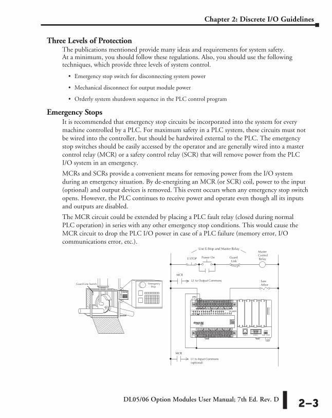
DL05/06 Option Modules User Manual; 7th Ed. Rev. D 2–3
Chapter 2: Discrete I/O Guidelines
Three Levels of ProtectionThe publications mentioned provide many ideas and requirements for system safety. At a minimum, you should follow these regulations. Also, you should use the following techniques, which provide three levels of system control.
• Emergency stop switch for disconnecting system power
• Mechanical disconnect for output module power
• Orderly system shutdown sequence in the PLC control program
Emergency StopsIt is recommended that emergency stop circuits be incorporated into the system for every machine controlled by a PLC. For maximum safety in a PLC system, these circuits must not be wired into the controller, but should be hardwired external to the PLC. The emergency stop switches should be easily accessed by the operator and are generally wired into a master control relay (MCR) or a safety control relay (SCR) that will remove power from the PLC I/O system in an emergency.
MCRs and SCRs provide a convenient means for removing power from the I/O system during an emergency situation. By de-energizing an MCR (or SCR) coil, power to the input (optional) and output devices is removed. This event occurs when any emergency stop switch opens. However, the PLC continues to receive power and operate even though all its inputs and outputs are disabled.
The MCR circuit could be extended by placing a PLC fault relay (closed during normal PLC operation) in series with any other emergency stop conditions. This would cause the MCR circuit to drop the PLC I/O power in case of a PLC failure (memory error, I/O communications error, etc.).
Emergency Stop
Guard Line SwitchSawArbor
E STOP
Power On
Use E-Stop and Master Relay
Guard Link
LOGIC
Koyo06
C0 C4C2X1 X3 X4 X6 X11 X13 X14 X16 X21 X23 N.C.
C1 C3X2 X5 X7 X10 X12 X15 X17 X20 X22X0 N.C.
AC(N) 24V
0V
N.C.
C1 C3Y0 Y15Y12Y10 Y17Y7Y5Y2
C0 C2 Y16Y14Y13Y11Y6Y4Y3Y1
LGG
AC(L)
D0-06DR2.0AOUTPUT: 6-240V 50 - 60Hz 2.0A, 6 - 27V
INPUT: 12 - 24V 3 - 15mA
Y
X
40VA50-60HzPWR: 100-240V
0 1 2 3 4 5 6 7 10 11 12 13 14 15 16 17 20 21 22 23
PORT1 PORT2
TERM
RUN STOP
PWR
RUN
CPU
TX1
RX1
TX2
RX2
Master Control Relay
MCR
L1 to Input Commons(optional)
MCR
L1 to Output Commons

DL05/06 Option Modules User Manual; 7th Ed. Rev. D2–4
Chapter 2: Discrete I/O Guidelines
Emergency Power DisconnectA properly rated emergency power disconnect should be used to power the PLC controlled system as a means of removing the power from the entire control system. It may be necessary to install a capacitor across the disconnect to protect against a condition known as “outrush”. This condition occurs when the output Triacs are turned off by powering off the disconnect, thus causing the energy stored in the inductive loads to seek the shortest distance to ground, which is often through the Triacs.
After an emergency shutdown or any other type of power interruption, there may be requirements that must be met before the PLC control program can be restarted. For example, there may be specific register values that must be established (or maintained from the state prior to the shutdown) before operations can resume. In this case, you may want to use retentive memory locations, or include constants in the control program to insure a known starting point.
Orderly System ShutdownIdeally, the first level of fault detection is the PLC control program, which can identify machine problems. Certain shutdown sequences should be performed. The types of problems are usually things such as jammed parts, etc. that do not pose a risk of personal injury or equipment damage.
WARNING: The control program must not be the only form of protection for any problems that may result in a risk of personal injury or equipment damage.
Class 1, Division 2 Approval (Applies ONLY to modules used with a DL06 PLC.)This equipment is suitable for use in Class 1, Division 2, groups A, B, C and D or non-hazardous locations only.
WARNING: Explosion Hazard! Substitution of components may impair suitability for Class 1, Division 2. Do not disconnect equipment unless power has been switched off or area is known to be non-hazardous.
JamDetect
RST
RST
Retract Arm
Turn off Saw

DL05/06 Option Modules User Manual; 7th Ed. Rev. D 2–5
Chapter 2: Discrete I/O Guidelines
System Wiring StrategiesThe DirectLOGIC Micro PLCs are very flexible and will work in many different wiring configurations. By studying this section before actual installation, you can probably find the best wiring strategy for your application . This will help to lower system cost, wiring errors, and avoid safety problems.
PLC Isolation BoundariesPLC circuitry is divided into three main regions separated by isolation boundaries, shown in the drawing below. Electrical isolation provides safety, so that a fault in one area does not damage another. A powerline filter will provide isolation between the power source and the power supply. A transformer in the power supply provides magnetic isolation between the primary and secondary sides. Opto-couplers provide optical isolation in Input and Output circuits. This isolates logic circuitry from the field side, where factory machinery connects. Note that the discrete inputs are isolated from the discrete outputs, because each is isolated from the logic side. Isolation boundaries protect the operator interface (and the operator) from power input faults or field wiring faults. When wiring a PLC, it is extremely important to avoid making external connections that connect logic side circuits to any other.
CPU
Input Circuit Main
PowerSupply
Discrete inputs
Power input
OutputCircuit
Primary Side Secondary, orLogic side
Field Side
PLC
Programming Device orOperator Interface
IsolationBoundary
IsolationBoundary
Filter
Discrete outputs

DL05/06 Option Modules User Manual; 7th Ed. Rev. D2–6
Chapter 2: Discrete I/O Guidelines
The following figures show the internal layout of the DL05 and DL06 PLCs, as viewed from the front panels.
Output CircuitInput Circuit
CPU 2 Comm.
Ports
Main
PowerSupply
To Programming Device
or Operator Interface
8 DiscreteInputs
Commons Commons6 Discrete OutputsPowerInput
PLC
DL05
Filter
Optional
I/O Circuits
Output Circuit
Input Circuit
CPU
2 Comm.
Ports
Main
PowerSupply
To Programming De-vice, Operator Interface
or networking20 Discrete Inputs
Commons
Commons16 Discrete Outputs
PowerInput
PLC
DL06
Filter
OptionalI/O Circuits

DL05/06 Option Modules User Manual; 7th Ed. Rev. D 2–7
Chapter 2: Discrete I/O Guidelines
Sinking/Sourcing Concepts
Before going further in our study of wiring strategies, we must have a solid understanding of “sinking” and “sourcing” concepts. Use of these terms occurs frequently in input or output circuit discussions. It is the goal of this section to make these concepts easy to understand, further ensuring your success in installation. First we give the following short definitions, followed by practical applications.
• Sinking = Path to supply ground (–)
• Sourcing = Path to supply source (+)
First you will notice that these are only associated with DC circuits and not AC, because of the reference to (+) and (–) polarities. Therefore, sinking and sourcing terminology only applies to DC input and output circuits. Input and output points that are either sinking or sourcing can conduct current in only one direction. This means it is possible to connect the external supply and field device to the I/O point with current trying to flow in the wrong direction, and the circuit will not operate. However, we can successfully connect the supply and field device every time by understanding “sourcing” and “sinking”.
For example, the figure to the right depicts a “sinking” input. To properly connect the external supply, we just have to connect it so the input provides a path to ground (–). So, we start at the PLC input terminal, follow through the input sensing circuit, exit at the common terminal, and connect the supply (–) to the common terminal. By adding the switch, between the supply (+) and the input, we have completed the circuit. Current flows in the direction of the arrow when the switch is closed.
By applying the circuit principle above to the four possible combinations of input/output sinking/sourcing types, we have the four circuits as shown below. DirectLOGIC Micro PLCs provide all except the sourcing output I/O circuit types.
+
–
InputSensing
PLC
Common
Input(sinking)
+
–
Input Sensing
Load
Sinking Input Sinking Output
Sourcing Input Sourcing Output
PLCInput
Common
+
–
OutputSwitch
PLCOutput
Common
+
–
Input Sensing
Load
PLC
Input
Common
+
–
OutputSwitch
PLC
Output
Common
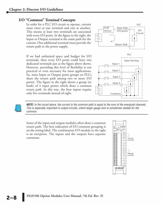
DL05/06 Option Modules User Manual; 7th Ed. Rev. D2–8
Chapter 2: Discrete I/O Guidelines
I/O “Common” Terminal ConceptsIn order for a PLC I/O circuit to operate, current must enter at one terminal and exit at another. This means at least two terminals are associated with every I/O point. In the figure to the right, the Input or Output terminal is the main path for the current. One additional terminal must provide the return path to the power supply.
If we had unlimited space and budget for I/O terminals, then every I/O point could have two dedicated terminals just as the figure above shows. However, providing this level of flexibility is not practical or even necessary for most applications. So, most Input or Output point groups on PLCs share the return path among two or more I/O points. The figure to the right shows a group (or bank) of 4 input points which share a common return path. In this way, the four inputs require only five terminals instead of eight.
NOTE: In the circuit above, the current in the common path is equal to the sum of the energized channels. This is especially important in output circuits, where larger gauge wire is sometimes needed for the common.
Some of the input and output modules often share a common return path. The best indication of I/O common grouping is on the wiring label. The combination I/O module to the right is an exception. The inputs and the outputs have separate commons.
+
–
I/O Circuit
Return Path
Main Path (I/O point)
FieldDevice
PLC
+
–
Input Sensing
Input 4
Common
Input 3
Input 2
PLC
Input 1

DL05/06 Option Modules User Manual; 7th Ed. Rev. D 2–9
Chapter 2: Discrete I/O Guidelines
Connecting DC I/O to Solid State Field DevicesIn the previous section on Sourcing/Sinking concepts, we explained that DC I/O circuits sometimes will only allow current to flow one way. This is also true for many of the field devices which have solid-state (transistor) interfaces. In other words, field devices can also be sourcing or sinking. When connecting two devices in a series DC circuit, one must be wired as sourcing and the other as sinking.
Solid State Input SensorsThe PLC DC inputs are flexible in that they detect current flow in either direction, so they can be wired as either sourcing or sinking. In the circuit below, a field device has an open-collector NPN transistor output. It sinks current from the PLC input point, which sources current. The source can be a FA-24PS, +24VDC, power supply or another supply (+12VDC or +24VDC) of your choice, as long as the input specifications are met.
In the circuit at right, a field device has an open-emitter PNP transistor output. It sources current to the PLC input point, which sinks the current back to ground. Since the field device is sourcing current, no additional power supply is required.
Solid State Output Loads Sometimes an application requires connecting a PLC output point to a solid state input on a device. This type of connection is usually made to carry a low-level signal, not to send DC power to an actuator.
Some of the optional DC output modules are sinking-only. This means that each DC output provides a path to ground when it is energized. The six outputs of the DL05 have the same electrical common, even though there are two common terminal screws. Not so with the DL06 which has four isolated commons. Finally, recall that the DC output circuit requires power (20–28 VDC) from an external power source.
In the circuit at right, the PLC output point sinks current to the output common when energized. It is connected to a sourcing input of a field device input.
Field Device
+–
PLC DC Input
Output
Ground
Common
Supply
(sinking)
Input(sourcing)
Field Device
PLC DC Input
Output (sourcing)
Ground Common
+V
Input
(sinking)
Field Device
Output
Ground
Input
Common
+V
PLC DC Output
+DC pwr
–
(sinking)
Power
20-28 VDC
+ (sourcing)

DL05/06 Option Modules User Manual; 7th Ed. Rev. D2–10
Chapter 2: Discrete I/O Guidelines
In the next example we connect a PLC DC output point to the sinking input of a field device. This is a bit tricky, because both the PLC output and field device input are sinking type. Since the circuit must have one sourcing and one sinking device, we add sourcing capability to the PLC output by using a pull-up resistor. In the circuit below, we connect Rpull-up from the output to the DC output circuit power input.
NOTE 1: DO NOT attempt to drive a heavy load (>25mA) with this pull-up method. NOTE 2: Using the pull-up resistor to implement a sourcing output has the effect of inverting the output point logic. In other words, the field device input is energized when the PLC output is OFF, from a ladder logic point-of-view. Your ladder program must comprehend this and generate an inverted output. Or, you may choose to cancel the effect of the inversion elsewhere, such as in the field device.
It is important to choose the correct value of Rpull-up. In order to do so, we need to know the nominal input current to the field device (I input) when the input is energized. If this value is not known, it can be calculated as shown (a typical value is 15mA). Then use I input and the voltage of the external supply to compute Rpull-up. Then calculate the power Ppull-up (in watts), in order to size Rpull-up properly.
Of course, the easiest way to drive a sinking input field device as shown below is to use a DC sourcing output module. The Darlington NPN stage will have about 1.5 V ON-state saturation, but this is not a problem with low-current solid-state loads.
Field Device
Output
Ground
Input
Common
Direct LOCIC DC Sourcing Output
+DC pwr
+
–
(sourcing)(sinking)
Supply
inputR
Field Device
Output
Ground
Input
Common
PLC DC Output
+DC pwr
+
–
(sourcing)
(sinking)
Power
(sinking)
pull-up
Supply
R
inputR
pull-upR inputR=supplyV – 0.7
–inputI
inputI =input (turn–on)V
inputR
pull-upP =supplyV 2
pullupR

DL05/06 Option Modules User Manual; 7th Ed. Rev. D 2–11
Chapter 2: Discrete I/O Guidelines
Relay Output GuidelinesRelay outputs are available for the DirectLOGIC PLCs. Relays are best for the following applications:
• Loads that require higher currents than the solid-state outputs can deliver
• Cost-sensitive applications
• Some output channels need isolation from other outputs (such as when some loads require different voltages than other loads)
Some applications in which NOT to use relays:
• Loads that require currents under 10mA
• Loads which must be switched at high speed or heavy duty cycle
Relay outputs in the DirectLOGIC PLCs and modules are available in two contact arrangements, shown to the right. The Form A type, or SPST (single pole, single throw) type is normally open and is the simplest to use. The Form C type, or SPDT (single pole, double throw) type has a center contact which moves and a stationary contact on either side. This provides a normally closed contact and a normally open contact.
Some relay output module’s relays share common terminals, which connect to the wiper contact in each relay of the bank. Other relay modules have relays which are completely isolated from each other. In all cases, the module drives the relay coil when the corresponding output point is on.
Prolonging Relay Contact LifeRelay contacts wear according to the amount of relay switching, amount of spark created at the time of open or closure, and presence of airborne contaminants. However, there are some steps you can take to help prolong the life of relay contacts:
• Switch the relay on or off only when the application requires it.
• If you have the option, switch the load on or off at a time when it will draw the least current.
• Take measures to suppress inductive voltage spikes from inductive DC loads such as contactors and solenoids (circuit given below).
Relay with Form A contacts
Relay with Form C contacts
Inductive Field Device
+ –
PLC Relay Output
Output
Common
Input
Common
Supply
R
C
DL05/06 Option Modules User Manual; 7th Ed. Rev. D2–12
Chapter 2: Discrete I/O Guidelines
Surge Suppression For Inductive LoadsInductive load devices (devices with a coil) generate transient voltages when de-energized with a relay contact. When a relay contact is closed it “bounces”, which energizes and de-energizes the coil until the “bouncing” stops. The transient voltages generated are much larger in amplitude than the supply voltage, especially with a DC supply voltage.
When switching a DC-supplied inductive load the full supply voltage is always present when the relay contact opens (or “bounces”). When switching an AC-supplied inductive load there is one chance in 60 (60Hz) or 50 (50Hz) that the relay contact will open (or “bounce”) when the AC sine wave is zero crossing. If the voltage is not zero when the relay contact opens there is energy stored in the inductor that is released when the voltage to the inductor is suddenly removed. This release of energy is the cause of the transient voltages.
When inductive load devices (motors, motor starters, interposing relays, solenoids, valves, etc.) are controlled with relay contacts, it is recommended that a surge suppression device be connected directly across the coil of the field device. If the inductive device has plug-type connectors, the suppression device can be installed on the terminal block of the relay output.
Transient Voltage Suppressors (TVS or transorb) provide the best surge and transient suppression of AC and DC powered coils, providing the fastest response with the smallest overshoot.
Metal Oxide Varistors (MOV) provide the next best surge and transient suppression of AC and DC powered coils.
For example, the waveform in the figure below shows the energy released when opening a contact switching a 24VDC solenoid. Notice the large voltage spike.
This figure shows the same circuit with a transorb (TVS) across the coil. Notice that the voltage spike is significantly reduced.
+24 VDC 0 VDC
Module Relay Contact
–324 VDC
+24 VDC
+24 VDC 0 VDC
Module Relay Contact
–42 VDC
+24 VDC

DL05/06 Option Modules User Manual; 7th Ed. Rev. D 2–13
Chapter 2: Discrete I/O Guidelines
Use the following table to help select a TVS or MOV suppressor for your application based on the inductive load voltage.
Prolonging Relay Contact LifeRelay contacts wear according to the amount of relay switching, amount of spark created at the time of open or closure, and presence of airborne contaminants. There are some steps you can take to help prolong the life of relay contacts, such as switching the relay on or off only when it is necessary, and if possible, switching the load on or off at a time when it will draw the least current. Also, take measures to suppress inductive voltage spikes from inductive DC loads such as contactors and solenoids.
For inductive loads in DC circuits we recommend using a suppression diode as shown in the following diagram (DO NOT use this circuit with an AC power supply). When the load is energized the diode is reverse-biased (high impedance). When the load is turned off, energy stored in its coil is released in the form of a negative-going voltage spike. At this moment the diode is forward-biased (low impedance) and shunts the energy to ground. This protects the relay contacts from the high voltage arc that would occur just as the contacts are opening.
Place the diode as close to the inductive field device as possible. Use a diode with a peak inverse voltage rating (PIV) at least 100 PIV, 3A forward current or larger. Use a fast-recovery type (such as Schottky type). DO NOT use a small-signal diode such as 1N914, 1N941, etc. Be sure the diode is in the circuit correctly before operation. If installed backwards, it short-circuits the supply when the relay energizes.
Inductive Field Device
+ –
PLC Relay Output
Output
Common
Input
Common
Supply
Surge SuppressorsVendor / Catalog Type Inductive Load Voltage Part Number
AutomationDirect
Transient Voltage Suppressors, LiteOn Diodes; from Digi-Key
Catalog: Phone: 1-800-344-4539
TVS TVS TVS TVS
Diode
110/120 VAC 24VDC
220/240 VAC 12/24 VDC 12/24 VDC
ZL-TD8-120 ZL-TD8-24
P6KE350CA P6K30CAGICT–ND
1N4004CT–ND
Digi-key www.digikey.com
MOV MOV
110/120 VAC 220/240 VAC Contact Digi-Key, Corp.

DL05/06 Option Modules User Manual; 7th Ed. Rev. D2–14
Chapter 2: Discrete I/O Guidelines
DC Input Wiring MethodsDirectLOGIC Micro PLCs with DC inputs are particularly flexible because they can be either sinking or sourcing. The dual diodes (shown to the right) allow current to flow in either direction. The inputs accept 10.8–26.4 VDC. The target applications are +12VDC and +24VDC. You can actually wire half of the inputs as DC sinking and the other half as DC sourcing. Inputs grouped by a common must be all sinking or all sourcing.
DC Output Wiring MethodsThe PLC DC output circuits are high-performance transistor switches with low on-resistance and fast switching times. Please note the following characteristics which are unique to the DC output type:
• The DL05 has only one electrical common for all six outputs. All six outputs belong to one bank.
• The DL05 output switches are current-sinking only. However, you can still use different DC voltages from one load to another.
• The DL06 has isolated commons for each group of four outputs. There are two DL06 models with output switches that are current-sinking only, and one that has sourcing output switches.
• The output circuit inside the PLC requires external power. The supply (–) must be connected to a common terminal, and the supply (+) connects the right-most terminal on the upper connector.
Firmware and SoftwareThe discrete option modules will only function properly in a DL05 with firmware version V4.10 (or later). If you have a DL05 with an earlier firmware version, the latest version can be downloaded from our website, www.automationdirect.com. If you are unable to download the latest firmware version along with the upgrade support tool software, call our technical support group to arrange to have your PLC upgraded.
The DL05 PLCs need to have DirectSOFT32 Version 3.0c (or later) in order for the analog feature to perform properly. The DL06 must use DirectSOFT32 Version 4.0 in order to use the option modules.
PLC DC Input
Common
Input
DL05/06 Option Modules User Manual; 7th Ed. Rev. D 2–15
Chapter 2: Discrete I/O Guidelines
I/O AddressingModule I/O Points and Addressing for the DL05 and DL06
Each discrete option module has a set number of I/O points. (This does not hold true for the analog modules). The following table shows the number of I/O points per module when used in the DL05 PLC or the first slot of a DL06 PLC that has a discrete module installed. Discrete I/O addressing for a DL06 is automatic from slot 1 to slot 4 by default.
NOTE: The information shown above is for Automatic I/O Configuration, which can assign addresses in groups as small as 8 I/O points. If manual I/O Configuration is used, the smallest allowable address group size is 16 I/O points. Therefore, each manually configured I/O module will consume at least 16 X (input) and/or 16 Y (output) addresses.
The diagrams on the next page show examples of the DL06 I/O addressing with various option modules installed.
DC Input Modules Physical I/O Points
Total I/O Points Consumed Slot 1 I/O Address
F0-08SIM 8 Input 8 Input X100 - X107D0-10ND3 10 Input 16 Input (6 unused) X100 - X107 and X110 - X111D0-10ND3F 10 Input (fast) 16 Input (6 unused) X100 - X107 and X110 - X111D0-16ND3 16 Input 16 Input X100 - X107 and X110 - X117
AC Input Modules Physical I/O Points
Total I/O Points Consumed Slot 1 I/O Address
F0-08NA-1 8 Input 8 Input* X100 - X107
DC Output Modules Physical I/O Points
Total I/O Points Consumed Slot 1 I/O Address
D0-10TD1 10 Output 16 Output (6 unused) Y100 - Y107 and Y110 - Y111D0-16TD1 16 Output 16 Output Y100 - Y107 and Y110 - Y117D0-10TD2 10 Output 16 Output (6 unused) Y100 - Y107 and Y110 - Y111D0-16TD2 16 Output 16 Output Y100 - Y107 and Y110 - Y117
Relay Output Modules Physical I/O Points
Total I/O Points Consumed Slot 1 I/O Address
D0-08TR 8 Output 8 Output* Y100 - Y107F0-04TRS 4 Output 8 Output (4 unused)* Y100 - Y103
Combination Modules Physical I/O Points
Total I/O Points Consumed Slot 1 I/O Address
D0-07CDR 4 Input, 3 Output 8 Input (4 unused)*, 8 Output (5 unused)* X100 - X103 and Y100 - Y102
D0-08CDD1 4 Input, 4 Output 8 Input (4 unused)*, 8 Output (4 unused)* X100 - X103 and Y100 - Y103

DL05/06 Option Modules User Manual; 7th Ed. Rev. D2–16
Chapter 2: Discrete I/O Guidelines
C0 C4C2X1 X3 X4 X6 X11 X13 X14 X16 X21 X23 N.C.
C1 C3X2 X5 X7 X10 X12 X15 X17 X20 X22X0 N.C.
AC(N) 24V
0V
N.C.
C1 C3Y0 Y15Y12Y10 Y17Y7Y5Y2
C0 C2 Y16Y14Y13Y11Y6Y4Y3Y1
LGG
AC(L)
2.0AOUTPUT: 6–240V 50 – 60Hz 2.0A, 6 – 27V
INPUT: 12 – 24V 3 – 15mA
Y
X
40VA50–60HzPWR: 100–240V
0 1 2 3 4 5 6 7 10 11 12 13 14 15 16 17 20 21 22 23
PORT1 PORT2
TERM
RUN STOP
PWR
RUN
CPU
TX1
RX1
TX2
RX2
D0–06DR
Slot 116pt Input (discrete)
Slot 24pt Input
X120
Slot 310pt Output (discrete)
Slot 48pt Output (discrete)4pt Output
(discrete)
X123
Y100
Y103
X100
X117
Y110
Y121
Y130
Y137
C0 C4C2X1 X3 X4 X6 X11 X13 X14 X16 X21 X23 N.C.
C1 C3X2 X5 X7 X10 X12 X15 X17 X20 X22X0 N.C.
AC(N) 24V
0V
N.C.
C1 C3Y0 Y15Y12Y10 Y17Y7Y5Y2
C0 C2 Y16Y14Y13Y11Y6Y4Y3Y1
LGG
AC(L)
2.0AOUTPUT: 6–240V 50 – 60Hz 2.0A, 6 – 27V
INPUT: 12 – 24V 3 – 15mA
Y
X
40VA50–60HzPWR: 100–240V
0 1 2 3 4 5 6 7 10 11 12 13 14 15 16 17 20 21 22 23
PORT1 PORT2
TERM
RUN STOP
PWR
RUN
CPU
TX1
RX1
TX2
RX2
D0–06DR
Slot 14pt Analog
Input
Slot 216pt Input(discrete)
X100
Slot 32pt Analog
Output
Slot 416pt Output(discrete)
X117
Y100
Y117
C0 C4C2X1 X3 X4 X6 X11 X13 X14 X16 X21 X23 N.C.
C1 C3X2 X5 X7 X10 X12 X15 X17 X20 X22X0 N.C.
AC(N) 24V
0V
N.C.
C1 C3Y0 Y15Y12Y10 Y17Y7Y5Y2
C0 C2 Y16Y14Y13Y11Y6Y4Y3Y1
LGG
AC(L)
2.0AOUTPUT: 6–240V 50 – 60Hz 2.0A, 6 – 27V
INPUT: 12 – 24V 3 – 15mA
Y
X
40VA50–60HzPWR: 100–240V
0 1 2 3 4 5 6 7 10 11 12 13 14 15 16 17 20 21 22 23
PORT1 PORT2
TERM
RUN STOP
PWR
RUN
CPU
TX1
RX1
TX2
RX2
D0–06DR
Slot 14pt Analog
Input
Slot 24pt Input
X100
Slot 3 Slot 416pt Input (discrete)4pt Output
(discrete)
X103
Y100
Y103
X120
X137
4pt Input
X110
4pt Output (discrete)
X113
Y110
Y113
All Discrete Modules Installed I/O Addressing Example:
Discrete and Analog Modules Installed I/O Addressing Example:
Discrete and Analog Modules Installed I/O Addressing Example:
DL05/06 Option Modules User Manual; 7th Ed. Rev. D 2–17
Chapter 2: Discrete I/O Guidelines
Discrete I/O General SpecificationsThe following is a list of general specifications for the discrete I/O option modules that are available for both the DL05 and DL06 PLCs. Also shown is information on the various removable connectors that are used for field wiring on the discrete I/O option modules along with reference to the ZIPLink connection system products that are available for the 16-point I/O modules.
General SpecificationsOperating Temperature 0 to 55 °C (32 to 131 °F) Shock MIL STD 810C 516.2Storage Temperature -20 to 70 °C (-4 to 158 °F) Hi-pot 1500VAC, 1 min.Humidity 5 to 95% (non-condensing) Insulation Resistance More than 10M ohms at 500VDCEnvironmental Air No Corrosive gases permitted Noise Immunity NEMA ICS3-304Vibration MIL STD 810C 514.2
Discrete I/O Connector Specifications
I/O Module Connector Wire Size Screw Torque
Screwdriver Size
D0-10ND3 AutomationDirect replacement terminal kit p/n D0-ACC-4 or use Dinkle: EC350, 13-pin. * 22–16 AWG 0.39 N·m TW-SD-VSL-1
(recommended)
D0-10ND3F AutomationDirect replacement terminal kit p/n D0-ACC-4 or use Dinkle: EC350, 13-pin. * 22–16 AWG 0.39 N·m TW-SD-VSL-1
(recommended)
D0-16ND3ZIPLink ZL-CBL056 cable & ZL-CM056 conn. mod. or ZL-CBL056L cable & ZL-CM16L24 LED conn. mod. or build your own using a 24-pin Molex Micro Fit 3.0 receptacle, p/n 43025, or compatible.
(see ZIPLink specifications in AutomationDirect catalog under “Connection” tab.)
F0-08NA-1 AutomationDirect replacement terminal kit p/n D0-ACC-4 or use Dinkle: EC350, 10-pin. * 22–16 AWG 0.39 N·m TW-SD-VSL-1
(recommended)
D0-10TD1 AutomationDirect replacement terminal kit p/n D0-ACC-4 or use Dinkle: EC350, 13-pin. * 22–16 AWG 0.39 N·m TW-SD-VSL-1
(recommended)
D0-16TD1
ZIPLink ZL-CBL056 cable & ZL-CM056 conn mod. or ZL-CBL056FR cable & ZL-CM16RL24B relay mod. or ZL-CM16TF2 fuse mod. or build your ownusing a 24-pin Molex Micro Fit 3.0 receptacle, p/n 43025, or compatible.
(see ZIPLink specifications in AutomationDirect catalog under “Connection” tab.)
D0-10TD2 AutomationDirect replacement terminal kit p/n D0-ACC-4 or use Dinkle: EC350, 13-pin. * 22–16 AWG 0.39 N·m TW-SD-VSL-1
(recommended)
D0-16TD2
ZIPLink ZL-CBL056 cable & ZL-CM056 conn. mod. or ZL-CBL056FR cable & ZL-CM16RL24B relay mod. or ZL-CM16TF2 fuse mod.or build your own using a 24-pin Molex Micro Fit 3.0 receptacle, p/n 43025, or compatible.
(see ZIPLink specifications in AutomationDirect catalog under “Connection” tab.)
D0-07CDR AutomationDirect replacement terminal kit p/n D0-ACC-4 or use Dinkle: EC350, 10-pin. * 22–16 AWG 0.39 N·m TW-SD-VSL-1
(recommended)
D0-08TR AutomationDirect replacement terminal kit p/n D0-ACC-4 or use Dinkle: EC350, 10-pin. * 22–16 AWG 0.39 N·m TW-SD-VSL-1
(recommended)
D0-08CDD1 AutomationDirect replacement terminal kit p/n D0-ACC-4 or use Dinkle: EC350, 13-pin. * 22–16 AWG 0.39 N·m TW-SD-VSL-1
(recommended)
F0-04TRS AutomationDirect replacement terminal kit p/n D0-ACC-4 or use Dinkle: EC350, 13-pin. * 22–16 AWG 0.39 N·m TW-SD-VSL-1
(recommended)* I/O modules are supplied with connector; replacement terminal kit includes (2) 13-position & (2) 10-position terminal blocks.

DL05/06 Option Modules User Manual; 7th Ed. Rev. D2–18
Chapter 2: Discrete I/O Guidelines
Glossary of Specification TermsDiscrete Input
One of the input connections to the PLC which converts an electrical signal from a field device to a binary status (OFF or ON), which is read by the internal CPU each PLC scan.
Discrete Output
One of the output connections from the PLC which converts an internal ladder program result (0 or 1) to turn ON or OFF an output switching device. This enables the program to turn ON and OFF large field loads.
I/O Common
A connection in the input or output terminals which is shared by multiple I/O circuits. It usually is in the return path to the power supply of the I/O circuit.
Input Voltage Range
The operating voltage range of the input circuit.
Maximum Voltage
Maximum voltage allowed for the input circuit.
ON Voltage Level
The minimum voltage level at which the input point will turn ON.
OFF Voltage Level
The maximum voltage level at which the input point will turn OFF
Input Impedance
Input impedance can be used to calculate input current for a particular operating voltage.
Input Current
Typical operating current for an active (ON) input.
Minimum ON Current
The minimum current for the input circuit to operate reliably in the ON state.
Maximum OFF Current
The maximum current for the input circuit to operate reliably in the OFF state.
OFF to ON Response
The time the module requires to process an OFF to ON state transition.
ON to OFF Response
The time the module requires to process an ON to OFF state transition.
Status Indicators
The LEDs that indicate the ON/OFF status of an input or output point. All LEDs on the Micro PLCs are electrically located on the logic side of the input or output circuit.

DL05/06 Option Modules User Manual; 7th Ed. Rev. D 2–19
Chapter 2: Discrete I/O Guidelines
NOTE: The DL05 CPU’s discrete feature for the F0-08SIM module requires DirectSOFT32 Version 3.0c (or later) and firmware version 4.90 (or later). The DL06 requires DirectSOFT32 version V4.0, build 16 (or later) and firmware version 1.80 (or later). See our website for more information: www.automationdirect.com.
F0-08SIM
ON OFF
0
1
2
3
4
5
6
7
F0-08SIM addressing example
C0 C4C2X1 X3 X4 X6 X11 X13 X14 X16 X21 X23 N.C.
C1 C3X2 X5 X7 X10 X12 X15 X17 X20 X22X0 N.C.
AC(N) 24V
0V
N.C.
C1 C3Y0 Y15Y12Y10 Y17Y7Y5Y2
C0 C2 Y16Y14Y13Y11Y6Y4Y3Y1
LGG
AC(L)
2.0AOUTPUT: 6–240V 50 – 60Hz 2.0A, 6 – 27V
INPUT: 12 – 24V 3 – 15mA
Y
X
40VA50–60HzPWR: 100–240V
0 1 2 3 4 5 6 7 10 11 12 13 14 15 16 17 20 21 22 23
PORT1 PORT2
TERM
RUN STOP
PWR
RUN
CPU
TX1
RX1
TX2
RX2
D0–06DR
Slot 24pt Input
X110
Slot 48pt Output(discrete)4pt Output
(discrete)
X113
Y100
Y103
X100
X107
X120
X127
Y110
Y117
F0-08SIM
ON OFF
0
1
2
3
4
5
6
7F0-08SIM
ON OFF
0
1
2
3
4
5
6
7
Input SpecificationsNumber of Inputs 8
Status Indicators None
Power Budget Requirements 1mA @ 5VDC (supplied by base)
Weight 45.36 g (1.6 oz.)
F0-08SIM 8-Point Simulator Input Module

DL05/06 Option Modules User Manual; 7th Ed. Rev. D2–20
Chapter 2: Discrete I/O Guidelines
12-24 VDC
12-24 VDC
Sink
Source
Sink
Source
Internal module circuitry
INPUT
COM
to LED
V+
12-24 VDC
Sink
Source
Derating chartEquivalent input circuit
D0-10ND3 10-Point DC Input Module
Input SpecificationsNumber of Inputs 10 (sink/source)Input Voltage Range 10.8–26.4 VDCOperating Voltage Range 12–24 VDCPeak Voltage 30.0 VDC
Input Current Typical: 4.0 mA @ 12VDC 8.5 mA @ 24VDC
Maximum Input Current 11mA @ 26.4 VDCInput Impedance 2.8 kq @ 12–24 VDCOn Voltage Level > 10.0 VDCOff Voltage Level < 2.0 VDCMinimum ON Current 3.5 mAMinimum OFF Current 0.5 mAOff to On Response 2–8 ms, Typ. 4msOn to Off Response 2–8 ms, Typ. 4ms
Status Indicators Module activity: one green LED (See page 1-6)
Commons 2 (5 pts/common) IsolatedFuse No fusePower Budget Requirements
35mA @ 5VDC (supplied by base), (all pts ON)
Dimensions (mm) 19.8(W) x 76.8(H) x 53.9(D)Weight 32g (1.13 oz.)
NOTE: The DL05 CPU’s discrete feature for this module requires DirectSOFT32 Version 3.0c (or later) and firmware version 4.10 (or later). The DL06 requires DirectSOFT32 version V4.0, build 16 (or later) and firmware version 1.00 (or later). See our website for more information: www.automationdirect.com.

DL05/06 Option Modules User Manual; 7th Ed. Rev. D 2–21
Chapter 2: Discrete I/O Guidelines
D0-10ND3F 10-Point DC Fast Input Module
Input SpecificationsNumber of Inputs 10 (sink/source)Input Voltage Range 10.8–26.4 VDC
Operating Voltage Range 12–24 VDC
Peak Voltage 30.0 VDC
Input Current Typical: 4.0 mA @ 12VDC 8.5 mA @ 24VDC
Maximum Input Current 11 mA @ 26.4 VDCInput Impedance 2.8 kq @ 12–24 VDCOn Voltage Level > 10.0 VDCOff Voltage Level < 2.0 VDCMinimum ON Current 3.5 mAMinimum OFF Current 0.5 mAOff to On Response 2ms, Typ. 1msOn to Off Response 2ms, Typ. 1ms
Status Indicators Module activity: one green LED (See page 1-6)
Commons 2 (5 pts/common) IsolatedFuse No fusePower Budget Requirements
35mA @ 5VDC (supplied by base), (all pts ON)
Dimensions (mm) 19.8(W) x 76.8(H) x 53.9(D)Weight 32g (1.13 oz.)
D0-10NDF
12-24 VDCSink
Source
12-24 VDCSink
Source
Internal module circuitry
INPUT
COM
to LED
V+
12-24 VDC
Sink
Source
Derating chartEquivalent input circuit
NOTE: The DL05 CPU’s discrete feature for this module requires DirectSOFT32 Version 3.0c (or later) and firmware version 4.70 (or later). The DL06 requires DirectSOFT32 version V4.0, build 16 (or later) and firmware version 1.50 (or later). See our website for more information: www.automationdirect.com.

DL05/06 Option Modules User Manual; 7th Ed. Rev. D2–22
Chapter 2: Discrete I/O Guidelines
D0-16ND3 16-Point DC Input Module
Internal module circuitry
INPUT
COM
to LED
V+
24 VDC
Sink
Source
24 V
DC
Sin
kS
ourc
e+
- +-
24 V
DC
Sin
kS
ourc
e+
- +-
24 V
DC
Sin
kS
ourc
e+
- +-
24 V
DC
Sin
kS
ourc
e+
- +-
Equivalent input circuit
Wiring for ZL-CM056
Use ZIPLink ZL-DO-CBL24L cable and ZL-RTB20 connector module, or ZL-DO-CBL24L cable and ZL-RRL16-24-1 relay module or ZL-RFU203 fuse module. You can also build your own cables using 24-pin Molex Micro Fit 3.0 receptacle, part number 43025, or compatible.
24VDC
Derating chart
Input SpecificationsNumber of Inputs 16 (sink/source)Input Voltage Range 20–28 VDCOperating Voltage Range 24VDCPeak Voltage 30.0 VDC
Input Current Typical: 4.0 mA @ 24VDC
Maximum Input Current 6mA @ 28VDCInput Impedance 4.7 kq @ 24VDCOn Voltage Level > 19.0 VDCOff Voltage Level < 7.0 VDCMinimum ON Current 3.5 mAMinimum OFF Current 1.5 mAOff to on Response 2–8 ms, Typ. 4msOn to off Response 2–8 ms, Typ. 4ms
Status IndicatorsModule activity: one green LED (See page 1-6)
Commons 4 (4 pts/common) Isolated
Fuse No fuse
Power Budget Requirements
35mA @ 5 VDC (supplied by base), (all pts ON)
Dimensions (mm) 19.8(W) x 76.8(H) x 53.9(D)
Weight 20g (0.71 oz.)
NOTE: The DL05 CPU’s discrete feature for this module requires DirectSOFT32 Version 3.0c (or later) and firmware version 4.10 (or later). The DL06 requires DirectSOFT32 version V4.0, build 16 (or later) and firmware version 1.00 (or later). See our website for more information: www.automationdirect.com.

DL05/06 Option Modules User Manual; 7th Ed. Rev. D 2–23
Chapter 2: Discrete I/O Guidelines
F0-08NA-1 8-Point AC Input Module
80-132VAC
F0-08NA-1
IN
90-150VDC
80-132V 50-60Hz90-150V
NOTE: The DL05 CPU’s discrete feature for this module requires DirectSOFT32 Version 3.0c (or later) and firmware version 4.70 (or later). The DL06 requires DirectSOFT32 version V4.0, build 16 (or later) and firmware version 1.50 (or later). See our website for more information: www.automationdirect.com.
Input SpecificationsNumber of Inputs 8Input Voltage Range 80–132 VAC (90–150 VDC)AC Frequency 47–63 HzInput Current 4.0 mA @ 132VACInput Impedance 33kq
On Voltage Level 80VAC minimumOff Voltage Level 20VAC maximumMinimum On Current 2.4 mAMaximum Off Current 1.6 mAOff to On Response < 20msOn to Off Response < 10msStatus Indicators NoneCommons 2 (4 pts/common) IsolatedFuse No fusePower Budget Requirements
5mA @ 5VDC (supplied by base), (all pts ON)
Dimensions (mm) 19.8(W) x 76.8(H) x 53.9(D)Weight 31.2 g (1.1 oz.)
Derating chartEquivalent input circuit

DL05/06 Option Modules User Manual; 7th Ed. Rev. D2–24
Chapter 2: Discrete I/O Guidelines
Load - SinglePower Source
Wiring
Load - DualPower Source
Wiring
Note: negative side of powersources must be tied togetherto both C0 & C1 terminals.
Internal module circuitry
Derating chartEquivalent output circuit
Output SpecificationsNumber of Outputs 10 (sinking)Operating Voltage Range 6–27 VDCOutput Voltage Range 5–30 VDCPeak Voltage 50.0 VDC
Maximum Output Current 0.3 A/point 1.5 A/common
Minimum Output Current 0.5 mAON Voltage Drop 0.5 VDC @ 0.3 AMaximum Leakage Current 15µA @ 30.0 VDCMaximum Inrush Current 1A for 10msOFF to ON Response <10µsON to OFF Response <60µs
Status Indicators Module activity: one green LED (See page 1-6)
Commons 2 (5 points/common) Non-isolated
Fuse No fuse
Power Budget Requirements
Max. 150mA @ 5VDC (supplied bybase), (all pts. ON)
External DC Power Required
20–28 VDC max. 200mA (all pts. ON)
Dimensions (mm) 19.8(W) x 76.8(H) x 53.9(D)Weight 34g (1.20 oz.)
D0-10TD1 10-Point DC Output Module
NOTE: The DL05 CPU’s discrete feature for this module requires DirectSOFT32 Version 3.0c (or later) and firmware version 4.10 (or later). The DL06 requires DirectSOFT32 version V4.0, build 16 (or later) and firmware version 1.00 (or later). See our website for more information: www.automationdirect.com.

DL05/06 Option Modules User Manual; 7th Ed. Rev. D 2–25
Chapter 2: Discrete I/O Guidelines
Output SpecificationsNumber of Outputs 16 (sinking)Operating Voltage Range 6–27 VDCOutput Voltage Range 5–30 VDCPeak Voltage 50.0 VDC
Maximum Output Current 0.1 A/point 0.8 A/common
Minimum Output Current 0.5 mAON Voltage Drop 0.5 VDC @ 0.1 AMaximum Leakage Current 15µA @ 30.0 VDC
Maximum Inrush Current 1A for 10msOFF to ON Response < 0.5 msON to OFF Response < 0.5 ms
Status Indicators Module activity: one green LED (See page 1-6)
Commons 2 (8 points/common) Non-isolated
Fuse No fuse
Power Budget Requirements
Max. 200mA @ 5VDC (supplied by base), (all pts. ON)
External DC Power Required
20–28 VDC max 70mA (all pts. ON)
Dimensions (mm) 19.8(W) x 76.8(H) x 53.9(D)Weight 22g (0.78 oz.)
Internal module circuitry
Wiring for DO-16TD1
Derating chart
Use ZIPLink ZL-DO-CBL24 cable and ZL-RTB20 connector module, or ZL-DO-CBL24 cable and ZL-RRL16-24-1 relay module or ZL-RFU203 fuse module. You can also build your own cables using 24-pin Molex Micro Fit 3.0 receptacle, part number 43025, or compatible.
D0-16TD1 16-Point DC Output ModuleEquivalent input circuit
Load - SinglePower Source
Wiring
Load - DualPower Source
Wiring
Note: negative side of powersources must be tied togetherto both C0 & C1 commons.
NOTE: The DL05 CPU’s discrete feature for this module requires DirectSOFT32 Version 3.0c (or later) and firmware version 4.10 (or later). The DL06 requires DirectSOFT32 version V4.0, build 16 (or later) and firmware version 1.00 (or later). See our website for more information: www.automationdirect.com.

DL05/06 Option Modules User Manual; 7th Ed. Rev. D2–26
Chapter 2: Discrete I/O Guidelines
D0-10TD2 10-Point DC Output Module
Load - SinglePower Source
Wiring
Load - DualPower Source
Wiring
Internal module circuitry12-24VDC
Equivalent output circuitDerating chart
Output SpecificationsNumber of Outputs 10 (sourcing)Operating Voltage Range 12–24 VDCOutput Voltage Range 10.8–26.4 VDCPeak Voltage 50.0 VDC
Maximum Output Current 0.3 A/point 1.5 A/common
Minimum Output Current 0.5 mAON Voltage Drop 1.0.VDC @0.3 AMaximum Leakage Current 1.5 µA @ 30.0 VDC
Maximum Inrush Current 1A for 10msOFF to ON Response <10µsON to OFF Response <60µs
Status Indicators Module activity: one green LED (See page 1-6)
+V Terminals & Common 2 (5 points/+V Terminal) Isolated, 1 Common
Fuse No fuse
Power Budget Requirements
Max. 150mA @ 5VDC (supplied by base), (all pts. ON)
Dimensions (mm) 19.8(W) x 76.8(H) x 53.9(D)Weight 38g (1.34 oz.)
NOTE: The DL05 CPU’s discrete feature for this module requires DirectSOFT32 Version 3.0c (or later) and firmware version 4.10 (or later). The DL06 requires DirectSOFT32 version V4.0, build 16 (or later) and firmware version 1.00 (or later). See our website for more information: www.automationdirect.com.
DL05/06 Option Modules User Manual; 7th Ed. Rev. D 2–27
Chapter 2: Discrete I/O Guidelines
D0-16TD2 16-Point DC Output Module
Internal module circuitry12-24VDC
Load - SinglePower Source
Wiring
Load - DualPower Source
Wiring
Equivalent output circuit
Wiring for ZL-RTB20
Derating chart
Use ZIPLink ZL-DO-CBL24 cable and ZL-RTB20 connector module, or ZL-DO-CBL24 cable and ZL-RRL16-24-1 relay module or ZL-RFU203 fuse module. You can also build your own cables using 24-pin Molex Micro Fit 3.0 receptacle, part number 43025, or compatible.
Output SpecificationsNumber of Outputs 16 (sourcing)Operating Voltage Range 12–24 VDCOutput Voltage Range 10.8–26.4 VDCPeak Voltage 50.0 VDCMaximum Output Current 0.1 A/point, 0.8 A/commonMinimum Output Current 0.5 mAON Voltage Drop 1.0.VDC @ 0.1 AMaximum Leakage Current 1.5 µA @ 26.4 VDC
Maximum Inrush Current 1A for 10msOFF to ON Response < 0.5 msON to OFF Response < 0.5 ms
Status Indicators Module activity: one green LED (See page 1-6)
+V Terminals & Common 2 (8 points/+V Terminal) Isolated, 1 Common
Fuse No fuse
Power Budget Requirements
Max. 200mA @ 5VDC (supplied bybase), (all pts. ON)
Dimensions (mm) 19.8(W) x 76.8(H) x 53.9(D)Weight 22g (0.78 oz.)
NOTE: The DL05 CPU’s discrete feature for this module requires DirectSOFT32 Version 3.0c (or later) and firmware version 4.10 (or later). The DL06 requires DirectSOFT32 version V4.0, build 16 (or later) and firmware version 1.00 (or later). See our website for more information: www.automationdirect.com.

DL05/06 Option Modules User Manual; 7th Ed. Rev. D2–28
Chapter 2: Discrete I/O Guidelines
D0-07CDR 4-Point DC Input, 3-Point Relay Output Module
12-24 VDCSink
Source
Internal module circuitry
INPUT
COM
to LED
V+
12-24 VDC
Sink
Source
Equivalent input circuitInternal module circuitry
Equivalent output circuit
Derating chart for DC inputs Derating chart for relay outputs
Input SpecificationsNumber of Inputs 4 (sink/source)Operating Voltage Range 12–24 VDCInput Voltage Range 10.8–26.4 VDCPeak Voltage 30.0 VDCMaximum Input Current 11mA @ 26.4 VDC
Input Current Typical: 4mA @ 12VDC 8.5 mA @ 24VDC
Input Impedance 2.8 kq @ 12–24 VDCON Voltage Level > 10.0 VDCOFF Voltage Level < 2.0 VDCMinimum ON Current 3.5 mAMaximum OFF Current 0.5 mAOFF to ON Response 2–8 ms, typical 4msON to OFF Response 2–8 ms, typical 4msCommons 1 (4 points/common)
Power Budget Requirements
Max. 200mA @ 5VDC (supplied by base), (all pts. ON)
Output SpecificationsNumber of Outputs 3Operating Voltage Range 6–27 VDC/6–240 VACOutput Type Relay, form A, SPSTPeak Voltage 30.0 VDC/ 264VACMaximum Current (Resistive) 1A / point, 4A / common
Minimum Load Current 5mA @ 5VDCMaximum Leakage Current 0.1 mA @ 264VACON Voltage Drop N/AMaximum Inrush Current Output: 3A for 10ms, Comm: 10A for 10msOFF to ON Response <15msON to OFF Response <10ms
Status Indicators Module activity: one green LED (See page 1-6)
Commons 1 (3 points/common)Fuse No fuseDimensions (mm) 19.8(W) x 76.8(H) x 53.9(D)Weight 38g (1.34 oz.)
NOTE: The DL05 CPU’s discrete feature for this module requires DirectSOFT32 Version 3.0c (or later) and firmware version 4.10 (or later). The DL06 requires DirectSOFT32 version V4.0, build 16 (or later) and firmware version 1.00 (or later). See our website for more information: www.automationdirect.com.

DL05/06 Option Modules User Manual; 7th Ed. Rev. D 2–29
Chapter 2: Discrete I/O Guidelines
D0-08TR 8-Point Relay Output Module
Internal module circuitry
Equivalent output circuit Derating chart
Output SpecificationsNumber of Outputs 8Operating Voltage Range 6–27 VDC/6–240 VACOutput Type Relay, form A, SPSTPeak Voltage 30.0 VDC/ 264VACMaximum Current (Resistive) 1A/point, 4A/common
Minimum Load Current 0.5 mAMaximum Leakage Current 0.1 mA @ 264VAC
ON Voltage Drop N/AMaximum Inrush Current Output: 3A for 10ms, Common: 10A for 10msOFF to ON Response <15msON to OFF Response <10msStatus Indicators Module activity: one green LED (See page 1-6)Commons 2 Isolated. (4 points/common)Fuse No fusePower Budget Requirements
Max. 280mA @ 5VDC (supplied by base), (all pts. ON)
Dimensions (mm) 19.8(W) x 76.8(H) x 53.9(D)Weight 55g (1.94 oz.)
NOTE: The DL05 CPU’s discrete feature for this module requires DirectSOFT32 Version 3.0c (or later) and firmware version 4.10 (or later). The DL06 requires DirectSOFT32 version V4.0, build 16 (or later) and firmware version 1.00 (or later). See our website for more information: www.automationdirect.com.

DL05/06 Option Modules User Manual; 7th Ed. Rev. D2–30
Chapter 2: Discrete I/O Guidelines
12-24 VDCSink
Source
D0-08CDD1 4-Point DC Input, 4-Point DC Output Module
Internal module circuitry
Equivalent output circuit
Output Derating chart
Internal module circuitry
INPUT
COM
to LED
V+
12-24 VDC
Sink
Source
Equivalent input circuit
Input Derating Chart
Input SpecificationsNumber of Inputs 4 (sink/source)Operating Voltage Range 10.8–26.4 VDCInput Voltage Range 12–24 VDCPeak Voltage 30.0 VDCMaximum Input Current 11mA @ 26.4 VDC
Input Current Typical: 4mA @ 12VDC 8.5 mA @ 24VDC
Input Impedance 2.8 kq @ 12–24VDCON Voltage Level > 10.0 VDCOFF Voltage Level < 2.0 VDCMinimum ON Current 3.5 mAMaximum OFF Current 0.5 mAOFF to ON Response 2–8 ms, typical 4msON to OFF Response 2–8 ms, typical 4msCommons 2 Non-isolatedExternal DC Power Required
20–28 VDC, max. 80mA (all pts. ON)
Power Budget Requiremnts
Max. 200mA @ 5VDC (supplied bybase), (all pts. ON)
Output SpecificationsNumber of Outputs 4 (sinking)Operating Voltage Range 6–27 VDC Output Voltage Range 5–30 VDCPeak Voltage 50.0 VDCMaximum Output Current 0.3 A/point, 1.2 A/commonMinimum Output Current 0.5 mA Maximum Leakage Current 1.5 µA @ 30.0 VDC
ON Voltage Drop 0.5 VDC @ 0.3 AMaximum Inrush Current 1A for 10msOFF to ON Response <10µsON to OFF Response <60µs
Status indicators Module acitivity: one green LED (See page 1-6)
Commons 2 Non-isolatedFuse No fuseDimensions (mm) 19.8(W) x 76.8(H) x 53.9(D)Weight 34g (1.20 oz.)
NOTE: The DL05 CPU’s discrete feature for this module requires DirectSOFT32 Version 3.0c (or later) and firmware version 4.10 (or later). The DL06 requires DirectSOFT32 version V4.0, build 16 (or later) and firmware version 1.00 (or later). See our website for more information: www.automationdirect.com.

DL05/06 Option Modules User Manual; 7th Ed. Rev. D 2–31
Chapter 2: Discrete I/O Guidelines
F0-04TRS
NO-0
NC-0
C-0
N0-1
C-1
NO-2
C-2
NO-3
NC-3
C-3
RELAY
L
L
L
L
L
L
5-30VDC5-125VAC
5-30VDC5-125VAC
5-30VDC5-125VAC
5-30VDC5-125VAC
OUT125V 3A50-60Hz30V 3A
Output SpecificationsNumber of Outputs 4Operating Voltage Range 5–30 VDC/ 5–125 VAC
Output Type 2 - form C (SPDT) 2 - form A (SPST normally open)
Peak Voltage 60 VDC/ 220 VACAC Frequency 47–63 HzMaximum Current 3A per point, General UseMinimum Load Current 10mA @ 5VDCMaximum Leakage Current N/A
ON Voltage Drop N/AMaximum Inrush Current 3AOFF to ON Response m 5ms (typical)ON to OFF Response m 5ms (typical)Status Indicators NoneCommons 4 IsolatedFuse 4, IEC 3.15 A, replaceable, D2-FUSE-1Power Budget Requirements
Max. 250mA @ 5VDC (supplied by base), (all pts. ON)
Dimensions (mm) 19.8(W) x 76.8(H) x 53.9(D)Weight 51g (1.8 oz.)
L
Common
NO
Internal Circuitry3.15A
Equivalent output circuit
L
Common
NO
NCL
Internal Circuitry
3.15A
Equivalent output circuit
3A
Derating chartNOTE: The DL05 CPU’s discrete feature for this module requires DirectSOFT32 Version 3.0c (or later) and firmware version 4.70 (or later). The DL06 requires DirectSOFT32 version V4.0, build 16 (or later) and firmware version 1.50 (or later). See our website for more information: www.automationdirect.com.
F0-04TRS Typical Relay Life at 30 Operations per Minute
Load Type Rated Voltage
Rated Current
Number of Operations
Resistive 120VAC 3A 120,000Resistive 120VAC 1A 550,000Resistive 24VDC 1A L2M
Inductive: SC-E5 Motor Starter 120VAC 0.1 A operating
1.7 A fault L2M (see Note)
Note: Transient suppression must be installed with inductive loads. (For example: P6KE150CA)
F0-04TRS 4-Point Relay Output Module

F0-04AD-1, 4-ChAnnel AnAlog Current Input 233
ChapterChapterChapter
In This Chapter...Module Specifications ...............................................................................................3–2
Setting the Module Jumper .......................................................................................3–4
Connecting and Disconnecting the Field Wiring .....................................................3–4
Wiring Diagram .........................................................................................................3–5
Module Operation .....................................................................................................3–6
Special V-memory Locations .....................................................................................3–7
Using the Pointer in Your Control Program .............................................................3–9
Detecting Input Signal Loss ....................................................................................3–11
Scale Conversions ....................................................................................................3–11
Special Relays ...........................................................................................................3–13
Module Resolution ...................................................................................................3–15
Analog Input Ladder Logic Filter ............................................................................3–16

DL05/06 Option Modules User Manual; 7th Ed. Rev. D3–2
Chapter 3: F0-04AD-1, 4-Channel Analog Current Input
Module SpecificationsThe F0-04AD-1 Analog Input module offers the following features:
• The DL05 and DL06 will read all four channels in one scan.
• The removable terminal block makes it possible to remove the module without disconnecting the field wiring.
• Analog inputs can be used as process variables for the four (4) PID loops in the DL05 and the eight (8) PID loops in the DL06 CPUs.
• Field device burn–out is detected on all four channels when 4–20mA range is selected.
• On-board active analog filtering and RISC-like microcontroller provide digital signal processing to maintain precise analog measurements in noisy environments.
NOTE: The DL05 CPU’s analog feature for this module requires DirectSOFT32 Version 3.0c (or later) and firmware version 2.10 (or later). The DL06 requires DirectSOFT32 version V4.0, build 16 (or later) and firmware version 1.00 (or later). See our website for more information: www.automationdirect.com.

DL05/06 Option Modules User Manual; 7th Ed. Rev. D 3–3
Chapter 3: F0-04AD-1, 4-Channel Analog Current Input
The following tables provide the specifications for the F0–04AD–1 Analog Input Module. Review these specifications to make sure the module meets your application requirements.
Input SpecificationsNumber of Channels 4, single ended (one common)Input Range 0 to 20mA or 4 to 20mA current (jumper selectable)Resolution 12 bit (1 in 4096) for 0–20 mA, scaled for 4–20 mAStep Response 25.0 ms (typ) to 95% of full step changeCrosstalk -80 dB, 1/2 count maximum *Active Low-pass Filtering -3dB at 40Hz (-12 dB per octave)Input Impedance 125 Ohm ± 0.1%, 1/8 W current inputAbsolute Maximum Ratings -30mA to +30mA current inputConverter type Successive approximationLinearity Error (End to End) ± 2 counts maximum *Input Stability ± 1 count *Full Scale Calibration Error(Offset error not included)
± 10 counts maximum, @ 20mA current input*
Offset Calibration Error ± 5 counts maximum @ 4mA current input *
Maximum Inaccuracy ± 0.4% @ 25°C (77°F)± 0.85% 0 to 60°C (32 to 140°F)
Accuracy vs. Temperature ±100ppm /°C maximum full scale calibration(Including maximum offset change)
Recommended Fuse (external) 0.032 A Series 217 fast-acting current inputs* One count in the specification table is equal to one least significant bit of the analog data value (1 in 4096).
General SpecificationsPLC Update Rate 4 channels per scan16-bit Data Word 12 binary data bitsOperating Temperature 0 to 60° C (32 to 140°F)Storage Temperature -20 to 70°C (-4 to 158°F)Relative Humidity 5 to 95% (non-condensing)Environmental air No corrosive gases permittedVibration MIL STD 810C 514.2Shock MIL STD 810C 516.2Noise Immunity NEMA ICS3-304Power Budget Requirement 50mA @ 5VDC (supplied by base)Connector Phoenix Mecano, Inc. Part No. AK1550/8-3.5 - greenConnector Wire Size 28–16 AWGConnector Screw Torque 0.4 N·mConnector Screwdriver Size DN-SS1 (recommended)

DL05/06 Option Modules User Manual; 7th Ed. Rev. D3–4
Chapter 3: F0-04AD-1, 4-Channel Analog Current Input
Setting the Module JumperThe position of jumper J3 determines the input signal level. You can choose between 4–20 mA and 0–20 mA. The module ships with the jumper not connecting the two pins. In this position, the expected input signal is 4–20 mA. To select 0–20 mA signals, use the jumper to cover both pins.
The default jumper setting selects a 4–20 mA signal source. The default jumper setting does not connect the two pins.
WARNING: Before removing the analog module or the terminal block on the face of the module, disconnect power to the PLC and all field devices. Failure to disconnect power can result in damage to the PLC and/or field devices.
Connecting and Disconnecting the Field WiringWiring Guidelines
Your company may have guidelines for wiring and cable installation. If so, you should check those before you begin the installation. Here are some general things to consider:
• Use the shortest wiring route whenever possible.
• Use shielded wiring and ground the shield at the transmitter source. Do not ground the shield at both the module and the source.
• Do not run the signal wiring next to large motors, high current switches, or transformers. This may cause noise problems.
• Route the wiring through an approved cable housing to minimize the risk of accidental damage. Check local and national codes to choose the correct method for your application.
The F0–04AD–1 does not supply power to field devices. You will need to power transmitters separately from the PLC.
To remove the terminal block, disconnect power to the PLC and the field devices. Pull the terminal block firmly until the connector separates from the module.
You can remove the analog module from the PLC by folding out the retaining tabs at the top and bottom of the module. As the retaining tabs pivot upward and outward, the module’s connector is lifted out of the PLC socket. Once the connector is free, you can lift the module out of its slot.
J3
OF
F = 4 – 20

DL05/06 Option Modules User Manual; 7th Ed. Rev. D 3–5
Chapter 3: F0-04AD-1, 4-Channel Analog Current Input
Wiring DiagramUse the following diagram to connect the field wiring. If necessary, the F0–04AD–1 terminal block can be removed to make removal of the module possible without disturbing field wiring.
Current Loop Transmitter ImpedanceManufacturers of transmitters and transducers specify a wide variety of power sources for their products. Follow the manufacturer’s recommendations.
In some cases, manufacturers specify a minimum loop or load resistance that must be used with the transmitter. The F0-04AD-1 provides 125 ohm resistance for each channel. If your transmitter requires a load resistance below 125 ohms, you do not have to make any changes. However, if your transmitter requires a load resistance higher than 125 ohms, you need to add a resistor in series with the module.
Consider the following example for a transmitter being operated from a 30 VDC supply with a recommended load resistance of 750 ohms. Since the module has a 125 ohm resistor, you need to add an additional resistor.
R = Tr–Mr R = resistor to add
R = 750–125 Tr = Transmitter Requirement
R M 625 Mr = Module resistance (internal 125 ohms)
CH14–wire
4–20mATransmitter
OV
A to DConverter
InternalModuleWiring
Analo
g S
witc
h
See NOTE 1
CH23–wire
4–20mATransmitter
CH32-wire
4–20mATransmitter
CH42-wire
4–20mATransmitter
+
–
+
–
+
–
+
–
–+
+
Typical User Wiring
+–
18-30VDC
Supply
Transmitter Supply
++
++
–
–
–
–
CH1–
CH2–
CH3–
CH4–
CH4+
CH3+
CH2+
CH1+
125 ohms
125 ohms
125 ohms
125 ohms
1+
–
2+
–
3+
–
4+
– CH
4+–
CH
3+–
CH
2+–
CH
1+–
PW R
R U N
C P U
T X 1
R X 1
T X 2
R X 2
A n a lo g In pu t4 –CH A NN ELS
0– 20m A4– 20m A
F0– 04AD–1
NOTE 1: Shields should be grounded at the signal
source.
NOTE 2: Connect all external power supply com-
mons.
NOTE 3: A Series 217, 0.032A fast–acting fuse is
recommended for current loops.
0V+30V
DC Supply
Two-wire Transmitter+ – Module Channel 1
R
125 ohmsCOM
0V
CH1

DL05/06 Option Modules User Manual; 7th Ed. Rev. D3–6
Chapter 3: F0-04AD-1, 4-Channel Analog Current Input
Module OperationChannel Scanning Sequence
The DL05 and DL06 will read all four channels of input data during each scan. Each CPU supports special V-memory locations that are used to manage the data transfer. This is discussed in more detail beginning in the section on “Special V-memory Locations”.
Analog Module UpdatesEven though the channel updates to the CPUs are synchronous with the CPU scan, the module asynchronously monitors the analog transmitter signals and converts each signal into a 12-bit binary representation. This enables the module to continuously provide accurate measurements without slowing down the discrete control logic in the RLL program.
The module takes approximately 25 milliseconds to sense 95% of the change in the analog signal. For the vast majority of applications, the process changes are much slower than these updates.
NOTE: If you are comparing other manufacturers’ update times (step responses) with ours, please be aware that some manufacturers refer to the time it takes to convert the analog signal to a digital value. Our analog to digital conversion takes only a few microseconds. It is the settling time of the filter that is critical in determining the full update time. Our update time specification includes the filter settling time.
Read the data
Store data
Read Inputs
Execute Application Program
Scan
Write to Outputs
Ch 1, 2, 3, 4Scan N
Scan N+1
Scan N+2
Scan N+3
Scan N+4
Ch 1, 2, 3, 4
Ch 1, 2, 3, 4
Ch 1, 2, 3, 4
Ch 1, 2, 3, 4
DL05/DL06 PLC

DL05/06 Option Modules User Manual; 7th Ed. Rev. D 3–7
Chapter 3: F0-04AD-1, 4-Channel Analog Current Input
Special V-memory LocationsFormatting the Module Data
The DL05 and DL06 PLCs have special V-memory locations assigned to their respective option slots. These V-memory locations allow you to:
• Specify the data format (binary or BCD)
• Specify the number of channels to scan (4 channels for the F0–04AD–1)
• Specify the V-memory locations to store the input data
DL05 Data FormattingThe table below shows the special V-memory locations used by the DL05 PLC for the F0–04AD–1.
Structure of V7700Special V-memory location 7700 indicates that a F0–04AD–1 module is installed in the DL05 option slot and the data type to be either binary or BCD.
Loading a constant of 400 into V7700 identifies a 4-channel analog input module is installed in the DL05 option slot, and reads the input data values as BCD numbers.
Loading a constant of 8400 into V7700 identifies a 4-channel analog input module is installed in the DL05 option slot, and reads the input data values as binary numbers.
Structure of V7701V7701 is a system V-memory location used as a pointer to a user V-memory location where the analog input data is stored. The V-memory location loaded into V7701 is an octal number identifying the first user V-memory location for reading the analog input data. This V-memory location is user selectable. For example, loading O2000 causes the pointer to write Ch 1’s data value to V2000, Ch 2’s data value to V2001, Ch 3’s data value to V2002, and Ch 4’s data value to V2003.
You will find an example program that loads appropriate values to V7700 and V7701 on page 3–9.
MSB LSB
15
014
13
12
11
10
9 8 7 6 5 4 3 2 1
MSB LSB
15
014
13
12
11
10
9 8 7 6 5 4 3 2 1
Analog Input Module DL05 Special V-memory Locations
Data Type and Number of Channels V7700Storage Pointer V7701

DL05/06 Option Modules User Manual; 7th Ed. Rev. D3–8
Chapter 3: F0-04AD-1, 4-Channel Analog Current Input
DL06 Data FormattingSpecial V-memory locations are assigned to the four option slots of the DL06 PLC. The table below shows these V-memory locations which can be used to setup the F0–04AD–1.
Setup Data Type and Number of ChannelsV-memory locations 700, 710, 720 and 730 are used to set the data format to be read in either binary or BCD, and to set the number of channels that will be active.
For example, the F0–04AD–1 is installed in slot 1. Loading a constant of 400 into V700 sets 4 channels active, and the input data value is read as a BCD number.
With the F0–4AD–1 in slot 1, loading a constant of 8400 into V700 sets 4 channels active, and the input data value is read as a binary number.
Storage Pointer SetupV-memory locations 701, 711, 721 and 731 are special locations used as storage pointers. A V-memory address is loaded into this location as an octal number identifying the first user V-memory location for the analog input data. This V-memory location is user selectable. For example, loading O2000 causes the pointer to write Ch 1’s data value to V2000, Ch 2’s data value to V2001, Ch 3’s data value to V2002, and Ch 4’s data value to V2003.
You will find an example program that loads appropriate values to V700 and V701 beginning on page 3–10.
Analog Input Module DL06 Special V-memory Locations
Slot No. 1 2 3 4Data Type and Number of Channels V700 V710 V720 V730Storage Pointer V701 V711 V721 V731
MSB LSB
15
014
13
12
11
10
9 8 7 6 5 4 3 2 1
MSB LSB
15
014
13
12
11
10
9 8 7 6 5 4 3 2 1
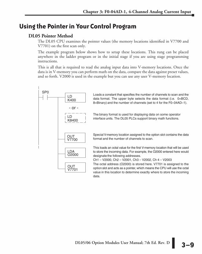
DL05/06 Option Modules User Manual; 7th Ed. Rev. D 3–9
Chapter 3: F0-04AD-1, 4-Channel Analog Current Input
Using the Pointer in Your Control ProgramDL05 Pointer Method
The DL05 CPU examines the pointer values (the memory locations identified in V7700 and V7701) on the first scan only.
The example program below shows how to setup these locations. This rung can be placed anywhere in the ladder program or in the initial stage if you are using stage programming instructions.
This is all that is required to read the analog input data into V-memory locations. Once the data is in V-memory you can perform math on the data, compare the data against preset values, and so forth. V2000 is used in the example but you can use any user V-memory location.
SP0LD
LDAO2000
OUTV7701
This loads an octal value for the first V-memory location that will be usedto store the incoming data. For example, the O2000 entered here woulddesignate the following addresses.Ch1 – V2000, Ch2 – V2001, Ch3 – V2002, Ch 4 – V2003The octal address (O2000) is stored here. V7701 is assigned to theoption slot and acts as a pointer, which means the CPU will use the octalvalue in this location to determine exactly where to store the incomingdata.
OUTV7700
Special V-memory location assigned to the option slot contains the dataformat and the number of channels to scan.
Loads a constant that specifies the number of channels to scan and thedata format. The upper byte selects the data format (i.e. 0=BCD,8=Binary) and the number of channels (set to 4 for the F0–04AD–1).
- or -The binary format is used for displaying data on some operatorinterface units. The DL05 PLCs support binary math functions.
K400
K8400LD

DL05/06 Option Modules User Manual; 7th Ed. Rev. D3–10
Chapter 3: F0-04AD-1, 4-Channel Analog Current Input
DL06 Pointer MethodUse the special V-memory table below as a guide to setup the storage pointer in the following example for the DL06. Slot 1 is the left most option slot. The CPU will examine the pointer values at these locations only after a mode transition.
The F0–04AD–1 can be installed in any available DL06 option slot. Using the example program from the previous page, but changing the V-memory addresses, the ladder diagram below shows how to setup these locations with the module installed in slot 1 of the DL06. Use the above table to determine the pointer values if locating the module in any of the other slot locations. Place this rung anywhere in the ladder program or in the initial stage if you are using stage programming instructions.
Like the DL05 example, this logic is all that is required to read the analog input data into V-memory locations. Once the data is in V-memory you can perform mathematical calculations with the data, compare the data against preset values, and so forth. V2000 is used in the example but you can use any user V-memory location.
Analog Input Module DL06 Special V-memory Locations
Slot No. 1 2 3 4No. of Channels V700 V710 V720 V730Input Pointer V701 V711 V721 V731
SP0LD
LDAO2000
OUTV701
This loads an octal value for the first V-memory location that will be usedto store the incoming data. For example, the O2000 entered here woulddesignate the following addresses.Ch1 – V2000, Ch2 – V2001, Ch3 – V2002, Ch 4 – V2003
The octal address (O2000) is stored here. V701 is assigned to thefirst option slot and acts as a pointer, which means the CPU will use the octal value in this location to determine exactly where to store the incoming data.
OUTV700
Special V-memory location assigned to the first option slot contains thedata format and the number of channels to scan.
Loads a constant that specifies the number of channels to scan and thedata format. The upper byte selects the data format (i.e. 0=BCD,8=Binary) and the number of channels (set to 4 for the F0–04AD–1).
- or -The binary format can be used for displaying data on someoperator interface units and the DL06 LCD display. The DL06PLCs support binary math functions.
K400
K8400LD

DL05/06 Option Modules User Manual; 7th Ed. Rev. D 3–11
Chapter 3: F0-04AD-1, 4-Channel Analog Current Input
Detecting Input Signal LossAnalog Signal Loss
The F0–04AD–1 analog module can sense the loss of analog input signals in 4–20 mA loops. The Special Relays described on page 3–14 allow you to use this feature in your ladder program. For example, in the rung below SP610 is used to pull-in coil Y1, which would be used to open or close an external circuit.
NOTE: The F0–04AD–1 analog module cannot sense the loss of analog input signals in 0–20 mA loops. See page 3–4 for information about setting the jumper to select your input type.
Scale ConversionsScaling the Input Data
Many applications call for measurements in engineering units, which can be more meaningful than raw data. Convert to engineering units using the formula shown to the right.
You may have to make adjustments to the formula depending on the scale you choose for the engineering units.
For example, if you wanted to measure pressure (PSI) from 0.0 to 99.9 then you would have to multiply the analog value by 10 in order to imply a decimal place when you view the value with the programming software or a handheld programmer. Notice how the calculations differ when you use the multiplier.
Analog Value of 2024, slightly less than half scale, should yield 49.4 PSI
Units = A H – L4095
Example without multiplier Example with multiplier
Units = 2024 100 – 04095
Units = 49
Units = 10 A H – L 4095
Units = 20240 100 – 0 4095
Units = 494
+ L
+ 0
+ L
+ 0
OUTY1
The Special Relay SP610 detectsa loss of input signal to channel 1.Use SP610 to trigger an alarm orshut down a machine.
SP610
Units = A H – L4095
H = High limit of the engineeringunit range
L = Low limit of the engineering unit range
A = Analog value (0 – 4095)
+ L

DL05/06 Option Modules User Manual; 7th Ed. Rev. D3–12
Chapter 3: F0-04AD-1, 4-Channel Analog Current Input
The Conversion ProgramThe following example shows how you would write the program to perform the engineering unit conversion. This example assumes you have BCD data loaded into the appropriate V-memory locations using instructions that apply for the model of CPU you are using.
Analog and Digital Value ConversionsSometimes it is useful to convert between the signal levels and the digital values. This is especially helpful during machine startup or troubleshooting. The following table provides formulas to make this conversion easier.
For example, if you have measured the signal as 10mA, you can use the formula to determine the digital value that will be stored in the V-memory location that contains the data.
LDV2000
SP1
MULK1000
DIVK4095
When SP1 is on, load channel 1 data to the accumulator.
Multiply the accumulator by 1000 (for a range of 0–1000).
Divide the accumulator by 4095 (the module resolution).
OUTV2010
Store the result in V2010.
Note: this example uses SP1, which is always on. Youcould also use an X, C, etc. permissive contact.
D =
D =
D = 2048
409520 A.
409520 10mA.
Range If you know the digital value If you know the analog signal level
4 to 20mA A = 16D + 4 4095
D = 4095 (A - 4) 16
0 to 20mA A = 20D 4095
D = 4095 20
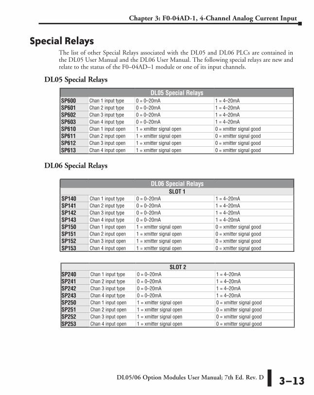
DL05/06 Option Modules User Manual; 7th Ed. Rev. D 3–13
Chapter 3: F0-04AD-1, 4-Channel Analog Current Input
Special RelaysThe list of other Special Relays associated with the DL05 and DL06 PLCs are contained in the DL05 User Manual and the DL06 User Manual. The following special relays are new and relate to the status of the F0–04AD–1 module or one of its input channels.
DL05 Special Relays
DL06 Special Relays
DL05 Special RelaysSP600 Chan 1 input type 0 = 0–20mA 1 = 4–20mASP601 Chan 2 input type 0 = 0–20mA 1 = 4–20mASP602 Chan 3 input type 0 = 0–20mA 1 = 4–20mASP603 Chan 4 input type 0 = 0–20mA 1 = 4–20mASP610 Chan 1 input open 1 = xmitter signal open 0 = xmitter signal goodSP611 Chan 2 input open 1 = xmitter signal open 0 = xmitter signal goodSP612 Chan 3 input open 1 = xmitter signal open 0 = xmitter signal goodSP613 Chan 4 input open 1 = xmitter signal open 0 = xmitter signal good
DL06 Special RelaysSLOT 1
SP140 Chan 1 input type 0 = 0–20mA 1 = 4–20mASP141 Chan 2 input type 0 = 0–20mA 1 = 4–20mASP142 Chan 3 input type 0 = 0–20mA 1 = 4–20mASP143 Chan 4 input type 0 = 0–20mA 1 = 4–20mASP150 Chan 1 input open 1 = xmitter signal open 0 = xmitter signal goodSP151 Chan 2 input open 1 = xmitter signal open 0 = xmitter signal goodSP152 Chan 3 input open 1 = xmitter signal open 0 = xmitter signal goodSP153 Chan 4 input open 1 = xmitter signal open 0 = xmitter signal good
SLOT 2SP240 Chan 1 input type 0 = 0–20mA 1 = 4–20mASP241 Chan 2 input type 0 = 0–20mA 1 = 4–20mASP242 Chan 3 input type 0 = 0–20mA 1 = 4–20mASP243 Chan 4 input type 0 = 0–20mA 1 = 4–20mASP250 Chan 1 input open 1 = xmitter signal open 0 = xmitter signal goodSP251 Chan 2 input open 1 = xmitter signal open 0 = xmitter signal goodSP252 Chan 3 input open 1 = xmitter signal open 0 = xmitter signal goodSP253 Chan 4 input open 1 = xmitter signal open 0 = xmitter signal good

DL05/06 Option Modules User Manual; 7th Ed. Rev. D3–14
Chapter 3: F0-04AD-1, 4-Channel Analog Current Input
DL06 Special Relays (cont’d)SLOT 3
SP340 Chan 1 input type 0 = 0–20 mA 1 = 4–20 mASP341 Chan 2 input type 0 = 0–20 mA 1 = 4–20 mASP342 Chan 3 input type 0 = 0–20 mA 1 = 4–20 mASP343 Chan 4 input type 0 = 0–20 mA 1 = 4–20 mASP350 Chan 1 input open 1 = xmitter signal open 0 = xmitter signal goodSP351 Chan 2 input open 1 = xmitter signal open 0 = xmitter signal goodSP352 Chan 3 input open 1 = xmitter signal open 0 = xmitter signal goodSP353 Chan 4 input open 1 = xmitter signal open 0 = xmitter signal good
SLOT 4SP440 Chan 1 input type 0 = 0–20 mA 1 = 4–20 mASP441 Chan 2 input type 0 = 0–20 mA 1 = 4–20 mASP442 Chan 3 input type 0 = 0–20 mA 1 = 4–20 mASP443 Chan 4 input type 0 = 0–20 mA 1 = 4–20 mASP450 Chan 1 input open 1 = xmitter signal open 0 = xmitter signal goodSP451 Chan 2 input open 1 = xmitter signal open 0 = xmitter signal goodSP452 Chan 3 input open 1 = xmitter signal open 0 = xmitter signal goodSP453 Chan 4 input open 1 = xmitter signal open 0 = xmitter signal good
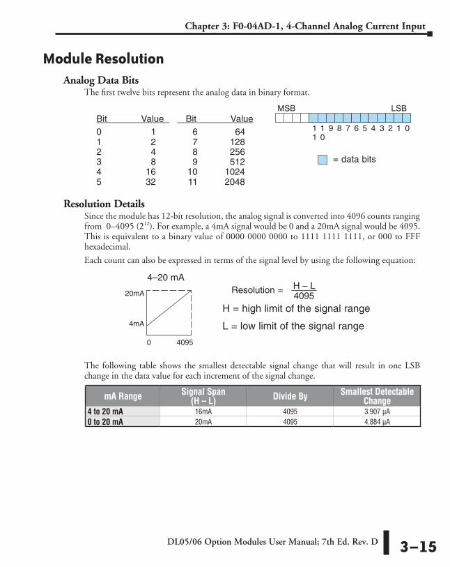
DL05/06 Option Modules User Manual; 7th Ed. Rev. D 3–15
Chapter 3: F0-04AD-1, 4-Channel Analog Current Input
Module ResolutionAnalog Data Bits
The first twelve bits represent the analog data in binary format.
Resolution DetailsSince the module has 12-bit resolution, the analog signal is converted into 4096 counts ranging from 0–4095 (212). For example, a 4mA signal would be 0 and a 20mA signal would be 4095. This is equivalent to a binary value of 0000 0000 0000 to 1111 1111 1111, or 000 to FFF hexadecimal.
Each count can also be expressed in terms of the signal level by using the following equation:
The following table shows the smallest detectable signal change that will result in one LSB change in the data value for each increment of the signal change.
20mA
4mA
0 4095
4–20 mAResolution = H – L
4095H = high limit of the signal range
L = low limit of the signal range
mA Range Signal Span (H – L) Divide By Smallest Detectable
Change4 to 20 mA 16mA 4095 3.907 µA0 to 20 mA 20mA 4095 4.884 µA
Bit Value Bit Value0 1 6 641 2 7 1282 4 8 2563 8 9 5124 16 10 10245 32 11 2048
MSB LSB
011
10
9 8 7 6 5 4 3 2 1
= data bits

DL05/06 Option Modules User Manual; 7th Ed. Rev. D3–16
Chapter 3: F0-04AD-1, 4-Channel Analog Current Input
Analog Input Ladder Logic FilterPID Loops / Filtering:
Please refer to the “PID Loop Operation” chapter in the DL06 or DL05 User Manual for information on the built-in PV filter (DL05/06) and the ladder logic filter (DL06 only) shown below. A filter must be used to smooth the analog input value when auto tuning PID loops to prevent giving a false indication of loop characteristics.
Smoothing the Input Signal (DL06 only):The filter logic can also be used in the same way to smooth the analog input signal to help stabilize PID loop operation or to stabilize the analog input signal value for use with an operator interface display, etc.
WARNING: The built-in and logic filters are not intended to smooth or filter noise generated by improper field device wiring or grounding. Small amounts of electrical noise can cause the input signal to bounce considerably. Proper field device wiring and grounding must be done before attempting to use the filters to smooth the analog input signal.
Using Binary Data Format
LDDV2000
SUBRV1400
BTOR
SP1Loads the analog signal, which is in binary formatand has been loaded from V–memory locationV2000 – 2001, into the accumulator. Contact SP1is always on.
OUTDV1400
ADDRV1400
MULRR0.2
OUTV2100
RTOB
Converts the binary value in the accumulatorto a real number.
Subtracts the real number stored in locationV1400 from the real number in the accumulator,and stores the result in the accumulator. V1400is the designated workspace in this example.
Multiplies the real number in the accumulator by0.2 (the filter factor), and stores the result in the accumulator. This is the filtered value. The filterrange is 0.1 to 0.9. Smaller filter factorsincrease filtering. (1.0 eliminates filtering.)
Adds the real number stored in location V1400 to the real number filtered value in the accumulator, and stores the result in the accumulator.
Copies the value in the accumulator tolocation V1400.
Converts the real number in theaccumulator to a binary value, andstores the result in the accumulator.
Loads the binary number filtered value fromthe accumulator into location V2100 to use inyour application or PID loop.

DL05/06 Option Modules User Manual; 7th Ed. Rev. D 3–17
Chapter 3: F0-04AD-1, 4-Channel Analog Current Input
NOTE: Be careful not to do a multiple number conversion on a value. For example, if you are using the pointer method in BCD format to get the analog value, it must be converted to binary (BIN) as shown below. If you are using the pointer method in Binary format, the conversion to binary (BIN) instruction is not needed.
Using BCD Data Format
LDV2000
SUBRV1400
BTOR
SP1
BIN
OUTDV1400
ADDRV1400
MULRR0.2
OUTV1402
BCD
RTOB
Loads the analog signal, which is in BCD formatand has been loaded from V–memory locationV2000, into the accumulator. Contact SP1is always on.
Converts the BCD value in the accumulatorto binary.
Subtracts the real number stored in locationV1400 from the real number in the accumulator,and stores the result in the accumulator. V1400is the designated workspace in this example.
Multiplies the real number in the accumulator by0.2 (the filter factor), and stores the result in the accumulator. This is the filtered value. The filterrange is 0.1 to 0.9. Smaller filter factorsincrease filtering. (1.0 eliminates filtering.)
Adds the real number stored in location V1400 to the real number filtered value in the accumulator, and stores the result in the accumulator.
Copies the value in the accumulator tolocation V1400.
Converts the real number in theaccumulator to a binary value, andstores the result in the accumulator.
Loads the BCD number filtered value fromthe accumulator into location V1402 to use inyour application or PID loop.
Converts the binary value in the accumulator to a real number.
Converts the binary value in the accumulatorto a BCD number. Note: The BCD instruction is not needed to PID loop PV (loop PV is a binary number).

F0-08ADH-1, 8-CHAnnel AnAlog Current Input 244
ChapterChapterChapter
In This Chapter...Module Specifications ...............................................................................................4–2
Connecting and Disconnecting the Field Wiring .....................................................4–4
Wiring Diagram .........................................................................................................4–5
Module Operation .....................................................................................................4–6
Special V-memory Locations .....................................................................................4–7
Using the Pointer in Your Control Program .............................................................4–9
Scale Conversions ....................................................................................................4–11
Module Resolution ...................................................................................................4–14
Analog Input Ladder Logic Filter ............................................................................4–15

DL05/06 Option Modules User Manual; 7th Ed. Rev. D4–2
Chapter 4: F0-08ADH-1, 8-Channel Analog Current Input
Module SpecificationsThe F0-08ADH-1 Analog Input module offers the following features:
• The DL05 and DL06 will read all eight channels in one scan.
• The removable terminal block simplifies module replacement.
• Analog inputs can be used as process variables for the four (4) PID loops in the DL05 and the eight (8) PID loops in the DL06 CPUs.
• On-board active analog filtering and RISC-like microcontroller provide digital signal processing to maintain precise analog measurements in noisy environments.
• These modules are isolated from the PLC power supply logic side (1800 Volt).
NOTE: The DL05 CPU’s analog feature for this module requires DirectSOFT32 Version 3.0c (or later) and firmware version 5.20 (or later). The DL06 requires DirectSOFT32 version V4.0, build 16 (or later) and firmware version 2.30 (or later). See our website for more information: www.automationdirect.com.
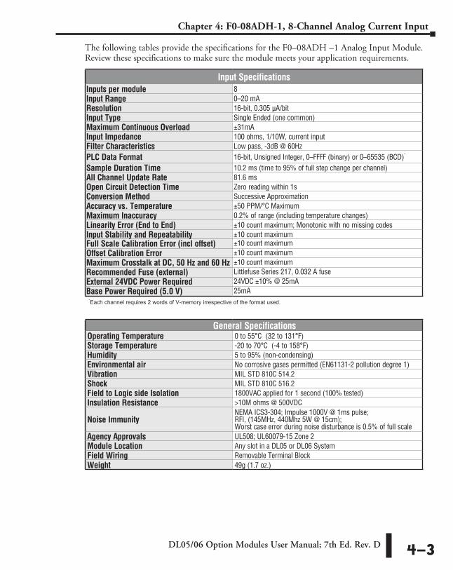
DL05/06 Option Modules User Manual; 7th Ed. Rev. D 4–3
Chapter 4: F0-08ADH-1, 8-Channel Analog Current Input
The following tables provide the specifications for the F0–08ADH –1 Analog Input Module. Review these specifications to make sure the module meets your application requirements.
Input SpecificationsInputs per module 8Input Range 0–20 mAResolution 16-bit, 0.305 µA/bitInput Type Single Ended (one common)Maximum Continuous Overload ±31mAInput Impedance 100 ohms, 1/10W, current inputFilter Characteristics Low pass, -3dB @ 60HzPLC Data Format 16-bit, Unsigned Integer, 0–FFFF (binary) or 0–65535 (BCD)*
Sample Duration Time 10.2 ms (time to 95% of full step change per channel)All Channel Update Rate 81.6 msOpen Circuit Detection Time Zero reading within 1sConversion Method Successive ApproximationAccuracy vs. Temperature ±50 PPM/°C MaximumMaximum Inaccuracy 0.2% of range (including temperature changes)Linearity Error (End to End) ±10 count maximum; Monotonic with no missing codesInput Stability and Repeatability ±10 count maximumFull Scale Calibration Error (incl offset) ±10 count maximum Offset Calibration Error ±10 count maximumMaximum Crosstalk at DC, 50 Hz and 60 Hz ±10 count maximumRecommended Fuse (external) Littlefuse Series 217, 0.032 A fuseExternal 24VDC Power Required 24VDC ±10% @ 25mABase Power Required (5.0 V) 25mA
General SpecificationsOperating Temperature 0 to 55°C (32 to 131°F)Storage Temperature -20 to 70°C (-4 to 158°F)Humidity 5 to 95% (non-condensing)Environmental air No corrosive gases permitted (EN61131-2 pollution degree 1)Vibration MIL STD 810C 514.2Shock MIL STD 810C 516.2Field to Logic side Isolation 1800VAC applied for 1 second (100% tested)Insulation Resistance >10M ohms @ 500VDC
Noise ImmunityNEMA ICS3-304; Impulse 1000V @ 1ms pulse; RFI, (145MHz, 440Mhz 5W @ 15cm); Worst case error during noise disturbance is 0.5% of full scale
Agency Approvals UL508; UL60079-15 Zone 2Module Location Any slot in a DL05 or DL06 SystemField Wiring Removable Terminal BlockWeight 49g (1.7 oz.)
*Each channel requires 2 words of V-memory irrespective of the format used.

DL05/06 Option Modules User Manual; 7th Ed. Rev. D4–4
Chapter 4: F0-08ADH-1, 8-Channel Analog Current Input
Connecting and Disconnecting the Field WiringWARNING: Before removing the analog module or the terminal block on the face of the module, disconnect power to the PLC and all field devices. Failure to disconnect power can result in damage to the PLC and/or field devices.
Wiring GuidelinesYour company may have guidelines for wiring and cable installation. If so, you should check those before you begin the installation. Here are some general things to consider:
• Use the shortest wiring route whenever possible.
• Use shielded wiring and ground the shield at the transmitter source. Do not ground the shield at both the module and the source.
• Do not run the signal wiring next to large motors, high current switches, or transformers. This may cause noise problems.
• Route the wiring through an approved cable housing to minimize the risk of accidental damage. Check local and national codes to choose the correct method for your application.
The F0–08ADH–1 does not supply power to field devices. You will need to power transmitters separately from the PLC.
To remove the terminal block, disconnect power to the PLC and the field devices. Pull the terminal block firmly until the connector separates from the module.
You can remove the analog module from the PLC by folding out the retaining tabs at the top and bottom of the module. As the retaining tabs pivot upward and outward, the module’s connector is lifted out of the PLC socket. Once the connector is free, you can lift the module out of its slot.
NOTE: The F0–08ADH–1 analog module cannot sense the loss of analog input signals in 0–20 mA loops.
Terminal Block SpecificationsNumber of Positions 13Re-Order Number D0-ACC-4Pitch 0.2 inch (5.08 mm)
Wire Range 28–16 AWG Solid or Stranded Conductor; Wire strip length 5/16” (7–8 mm)
Screwdriver Size (Slotted) 0.4T x 2.5W mm (part number DN-SS1)Screw Size M2.5 sizeScrew Torque 4.5 inch-pounds (0.52 N·m)

DL05/06 Option Modules User Manual; 7th Ed. Rev. D 4–5
Chapter 4: F0-08ADH-1, 8-Channel Analog Current Input
Wiring DiagramUse the following diagram to connect the field wiring. If necessary, the F0–08ADH–1 terminal block can be removed to make removal of the module possible without disturbing field wiring.
Current Loop Transmitter ImpedanceManufacturers of transmitters and transducers specify a wide variety of power sources for their products. Follow the manufacturer’s recommendations.
In some cases, manufacturers specify a minimum loop or load resistance that must be used with the transmitter. The F0-08ADH-1 provides 100 ohm resistance for each channel. If your transmitter requires a load resistance below 100 ohms, you do not have to make any changes. However, if your transmitter requires a load resistance higher than 100 ohms, you need to add a resistor in series with the module.
Consider the following example for a transmitter being operated from a 30VDC supply with a recommended load resistance of 750 ohms. Since the module has a 100 ohm resistor, you need to add an additional resistor.
R = Tr–Mr R = Resistor to add
R = 750–100 Tr = Transmitter requirement
R M 650 Mr = Module resistance (internal 100 ohms)
0V+30V
DC Supply
Two-wire Transmitter+ – Module Channel 1
R
125 ohmsCOM
0V
CH1
ANALOG
0–20mA
F0-08ADH-1
IN
CH1
CH2
CH3
CH4
COM
CH5
CH6
CH7
CH8
COM
COM
+24V
0V
2-wire 4–20mATransmitter
24VDCPower Supply
0VDC
+24VDC
COM
COM
COM
4-20mA TransmitterShield, Ch. 1
2-wire 4–20mATransmitter
.032AShield, Ch. 3
4-20mA Transmitter
4-wire 4–20mATransmitter
AC or DC CH5
+3-wire 4–20mATransmitter
CH3
CH1
CH8
Shield, Ch. 54-20mA Transmitter
Shield, Ch. 84-20mA Transmitter
Note 1: A Littelfuse Series 217, 0.032A fast-acting fuse is recommended for all 4-20mA current loops.Note 2: Do not connect both ends of shield.
SEE NOTE 1.
SHIELD CONNECTED TO SIGNALSOURCE COMMON. SEE NOTE 2.
CH1 ADC
CH2 ADC
CH3 ADC
CH4 ADC
CH5 ADC
CH6 ADC
CH7 ADC
CH8 ADC
100 Ω
0V
Internal Module CircuitryTypical User Wiring
100 Ω
100 Ω
100 Ω
100 Ω
100 Ω
100 Ω
100 Ω
ISOLATED ANALOGCIRCUIT POWER

DL05/06 Option Modules User Manual; 7th Ed. Rev. D4–6
Chapter 4: F0-08ADH-1, 8-Channel Analog Current Input
Module OperationChannel Scanning Sequence
The DL05 and DL06 will read all eight channels of input data during each scan. Each CPU supports special V-memory locations that are used to manage the data transfer. This is discussed in more detail beginning in the section on “Special V-memory Locations”.
Analog Module UpdatesEven though the channel updates to the CPUs are synchronous with the CPU scan, the module asynchronously monitors the analog transmitter signals and converts each signal into a 16-bit binary representation. This enables the module to continuously provide accurate measurements without slowing down the discrete control logic in the RLL program.
The module takes approximately 10.2 milliseconds to sense 95% of the change in the analog signal per channel. It takes approximately 81.6 ms to sample all channels.
NOTE: If you are comparing other manufacturers’ update times (step responses) with ours, please be aware that some manufacturers refer to the time it takes to convert the analog signal to a digital value. Our analog to digital conversion takes only a few microseconds. It is the settling time of the filter that is critical in determining the full update time. Our update time specification includes the filter settling time.
Read the data
Store data
Read Inputs
Execute Application Program
Scan
Write to Outputs
Scan N
Scan N+1
Scan N+2
Scan N+3
Scan N+4
DL05/DL06 PLC
Ch 1, 2, 3, 4, 5, 6, 7, 8
Ch 1, 2, 3, 4, 5, 6, 7, 8
Ch 1, 2, 3, 4, 5, 6, 7, 8
Ch 1, 2, 3, 4, 5, 6, 7, 8
Ch 1, 2, 3, 4, 5, 6, 7, 8

DL05/06 Option Modules User Manual; 7th Ed. Rev. D 4–7
Chapter 4: F0-08ADH-1, 8-Channel Analog Current Input
Special V-memory LocationsFormatting the Analog Module Data
The DL05 and DL06 PLCs have special V-memory locations assigned to their respective option slots. These V-memory locations allow you to:
• Specify the data format (binary or BCD)
• Specify the number of channels to scan (up to 8 channels for the F0–08ADH–1)
• Specify the V-memory locations to store the input data
DL05 Data FormattingThe table below shows the special V-memory locations used by the DL05 PLC for the F0–08ADH–1.
Setup Data Type and Number of Active ChannelsSpecial V-memory location 7700 is used to set the data format to either BCD or binary and to set the number of channels that will be active.
For example, assume the F0–08ADH–1 is installed in the option slot. Loading a constant of 800 into V7700 sets 8 channels active and causes the input data value to be read as a BCD number.
With the F0–08ADH–1 in the option slot, loading a constant of 8800 into V7700 sets 8 channels active, and the input data value is read as a binary number.
Storage Pointer SetupV7701 is a system V-memory location used as a pointer to a user V-memory location where the analog input data is stored. The V-memory location loaded into V7701 is an octal number identifying the first user V-memory location for reading the analog input data. This V-memory location is user selectable. For example, loading O2000 causes the pointer to write Ch 1’s data value to V2000 – 2001, Ch 2’s data value to V2002 – 2003, Ch 3’s data value to V2004 – 2005, Ch 4’s data value to V2006 – 2007, Ch 5’s data value to V2010 – 2011, Ch 6’s data value to V2012 – 2013, Ch 7’s data value to V2014 – 2015, and Ch 8’s data value to V2016 – 2017.
You will find an example program that loads appropriate values to V7700 and V7701 on page 4–9.
Analog Input Module DL05 Special V-memory Locations
Data Type and Number of Channels V7700Storage Pointer V7701
MSB LSB
0115
10
11
12
13
14
789 6 5 4 3 2
MSB LSB
0115
10
11
12
13
14
789 6 5 4 3 2
V7700 BCD setup
V7700 binary setup
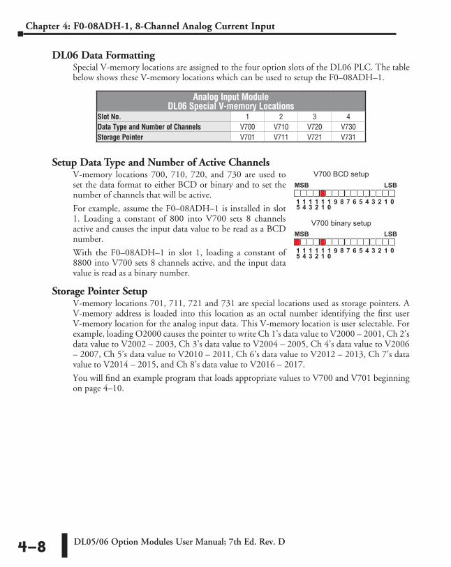
DL05/06 Option Modules User Manual; 7th Ed. Rev. D4–8
Chapter 4: F0-08ADH-1, 8-Channel Analog Current Input
DL06 Data FormattingSpecial V-memory locations are assigned to the four option slots of the DL06 PLC. The table below shows these V-memory locations which can be used to setup the F0–08ADH–1.
Setup Data Type and Number of Active ChannelsV-memory locations 700, 710, 720, and 730 are used to set the data format to either BCD or binary and to set the number of channels that will be active.
For example, assume the F0–08ADH–1 is installed in slot 1. Loading a constant of 800 into V700 sets 8 channels active and causes the input data value to be read as a BCD number.
With the F0–08ADH–1 in slot 1, loading a constant of 8800 into V700 sets 8 channels active, and the input data value is read as a binary number.
Storage Pointer SetupV-memory locations 701, 711, 721 and 731 are special locations used as storage pointers. A V-memory address is loaded into this location as an octal number identifying the first user V-memory location for the analog input data. This V-memory location is user selectable. For example, loading O2000 causes the pointer to write Ch 1’s data value to V2000 – 2001, Ch 2’s data value to V2002 – 2003, Ch 3’s data value to V2004 – 2005, Ch 4’s data value to V2006 – 2007, Ch 5’s data value to V2010 – 2011, Ch 6’s data value to V2012 – 2013, Ch 7’s data value to V2014 – 2015, and Ch 8’s data value to V2016 – 2017.
You will find an example program that loads appropriate values to V700 and V701 beginning on page 4–10.
Analog Input Module DL06 Special V-memory Locations
Slot No. 1 2 3 4Data Type and Number of Channels V700 V710 V720 V730Storage Pointer V701 V711 V721 V731
MSB LSB
0115
10
11
12
13
14
789 6 5 4 3 2
MSB LSB
0115
10
11
12
13
14
789 6 5 4 3 2
V700 BCD setup
V700 binary setup

DL05/06 Option Modules User Manual; 7th Ed. Rev. D 4–9
Chapter 4: F0-08ADH-1, 8-Channel Analog Current Input
Using the Pointer in Your Control ProgramDL05 Pointer Method Using Conventional Ladder Logic
NOTE: The proper use of the DL05 pointer requires that the V-memory address be written to the special memory location on the first scan only. Use the SP0 bit as a permissive contact when using the code shown below.
The example program below shows how to setup the special V-memory locations. This rung can be placed anywhere in the ladder program or in the initial stage if you are using stage programming instructions.
This is all that is required to read the analog input data into V-memory locations. Once the data is in V-memory you can perform math on the data, compare the data against preset values, and so forth. V2000 is used in the example but you can use any user V-memory location.
DL05 Pointer Method Using the IBox Instruction Available in DirectSOFT5The following logic accomplishes the same thing as the previous ladder example, but it uses the IBox instruction ANLGIN.
SP0LD
LDAO2000
OUTV7701
Ch1 – V2000-2001, Ch2 – V2002-V2003, Ch3 – V2004-V2005, Ch 4 – V2006-2007Ch 5 – V2010-2011, Ch 6 – V2012-V2013, Ch 7 – V2014-V2015, Ch 8 – V2016-V2017.
OUTV7700
Loads a constant that specifies the number of channels to scan and the data format. The upper byte selects the data format (i.e. 0=BCD, 8=Binary)and the number of channels (up to 8 for the F0-08ADH-1).
- or -
K800
K8800LD The binary format is used for displaying data on some operator
interface units. The DL05 PLCs support binary math functions.
Special V-memory location assigned to the option slot contains thedata format and the number of channels to scan.
This loads an octal value for the first V-memory location that will be usedto store the incoming data. For example, the O2000 entered here woulddesignate the following addresses:
The octal address (O2000) is stored here. V7701 is assigned to the option slot and acts as a pointer, which means the CPU will use the octal value in this location to determine exaclty where to store the incoming data.
Analog Input Module Pointer SetupANLGIN IB-460
Base # (K0 - Local)Slot #Number of Input ChannelsInput Data Format (0 - BCD 1 - BIN)Input Data Address
K0K1K8K0
V2000
No permissive contact or input logicis used with this instruction. This instructionoperates on the first scan only.

DL05/06 Option Modules User Manual; 7th Ed. Rev. D4–10
Chapter 4: F0-08ADH-1, 8-Channel Analog Current Input
DL06 Pointer Method Using Conventional Ladder Logic
NOTE: The proper use of the DL06 pointer requires that the V-memory address be written to the special memory location on the first scan only. Use the SP0 bit as a permissive contact when using the code shown below.
Use the special V-memory table below as a guide to setup the storage pointer in the following example for the DL06. Slot 1 is the left most option slot.
The F0–08ADH–1 can be installed in any available DL06 option slot. The ladder diagram below shows how to set up these locations with the module installed in slot 1 of the DL06. Use the above table to determine the pointer values if locating the module in any of the other slot locations. Place this rung anywhere in the ladder program or in the initial stage if you are using stage programming instructions.
This logic is all that is required to read the analog input data into V-memory locations. Once the data is in V-memory you can perform mathematical calculations with the data, compare the data against preset values, and so forth. In the example, V2000 is used, but you can use any user V-memory location.
Analog Input Module DL06 Special V-memory Locations
1 2 3 4No. of Channels V700 V710 V720 V730Input Pointer V701 V711 V721 V731
SP0LD
LDAO2000
OUTV701
OUTV700
K800
K8800LD
Ch1 – V2000-2001, Ch2 – V2002-V2003, Ch3 – V2004-V2005, Ch 4 – V2006-2007Ch 5 – V2010-2011, Ch 6 – V2012-V2013, Ch 7 – V2014-V2015, Ch 8 – V2016-V2017.
Loads a constant that specifies the number of channels to scan and the data format. The upper byte selects the data format (i.e. 0=BCD, 8=Binary)and the number of channels (up to 8 for the F0-08ADH-1).
The binary format is used for displaying data on some operatorinterface units and the DL06 display. The DL06 PLCs support binary math functions.
Special V-memory location assigned to the first option slot contains thedata format and the number of channels to scan.
This loads an octal value for the first V-memory location that will be usedto store the incoming data. For example, the O2000 entered here woulddesignate the following addresses:
The octal address (O2000) is stored here. V701 is assigned to the first option slot and acts as a pointer, which means the CPU will use the octal value in this location to determine exaclty where to store the incoming data.
- or -

DL05/06 Option Modules User Manual; 7th Ed. Rev. D 4–11
Chapter 4: F0-08ADH-1, 8-Channel Analog Current Input
DL06 Pointer Method Using the IBox Instruction Available in DirectSOFT6The following logic accomplishes the same thing as the previous ladder example, but it uses the IBox instruction ANLGIN.
Scale ConversionsScaling the Input Data
Many applications call for measurements in engineering units, which can be more meaningful than raw data. Convert to engineering units using the formula shown to the right.
You may have to make adjustments to the formula depending on the scale you choose for the engineering units.
For example, if you wanted to measure pressure (PSI) from 0.0 to 99.9 then you would have to multiply the analog value by 10 in order to imply a decimal place when you view the value with the programming software or a handheld programmer. Notice how the calculations differ when you use the multiplier.
Analog Value of 32375, slightly less than half scale, should yield 49.4 PSI.
Units = A H – LExample without multiplier Example with multiplier
Units = 100 – 0
Units = 49
Units = 10 x A H – L65535
Units = 323750 100 – 065535
Units = 494
+ L
+ 0
+ L
+ 0
65535
6553532375
Units = A H – L65535
H = High limit of the engineeringunit range
L = Low limit of the engineering unit range
A = Analog value (0 – 65535)
+ L
Analog Input Module Pointer SetupANLGIN IB-460
Base # (K0 - Local)Slot #Number of Input ChannelsInput Data Format (0 - BCD 1 - BIN)Input Data Address
K0K1K8K0
V2000
No permissive contact or input logicis used with this instruction. This instructionoperates on the first scan only.

DL05/06 Option Modules User Manual; 7th Ed. Rev. D4–12
Chapter 4: F0-08ADH-1, 8-Channel Analog Current Input
The Conversion Program in Standard Ladder LogicThe following example shows how you would write the program to perform the engineering unit conversion. This example assumes you have BCD data loaded into the appropriate V-memory locations using instructions that apply for the model of CPU you are using.
SP0LDD
LDDK65535
OUTDV3002
OUTDV3000
K100
SP1LDD
DIVDV3002
OUTDV2100
MULDV3000
V2000
Loads the constant 100 to the accumulator.
Copies the constant 100 from the accumulatorto the memory location V3000 and V3001.
Loads the constant 65535 to the accumulator.
Copies the content of V2000 from the accumulatorto the memory location V3002 and V3003.
_First Scan
_On
Loads data from V2000 and V2001.
Multiplies the accumulator value by 100 (previously loaded into V3000 and V3001).
Divides the accumulator value by 65535 (previously loaded into V3002 and V3003).
Copies the content of the accumulator to the memory location V2100 and V2101.
32375
V2000/2001
49
V2100/2101

DL05/06 Option Modules User Manual; 7th Ed. Rev. D 4–13
Chapter 4: F0-08ADH-1, 8-Channel Analog Current Input
Analog and Digital Value ConversionsSometimes it is useful to convert between the signal levels and the digital values. This is especially helpful during machine start-up or troubleshooting. The following table provides formulas to make this conversion easier.
For example, if you have measured the signal as 10mA, you can use the formula to determine the digital value that should be stored in the V-memory location that contains the data.
D =
D =
D = 32767
6553520 A.
6553520 10mA.
Range If you know the digital value If you know the analog signal level
0 to 20mA A = . D65535
20 D = . A6553520
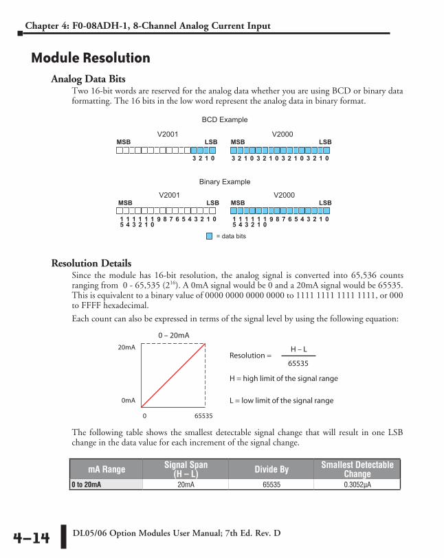
DL05/06 Option Modules User Manual; 7th Ed. Rev. D4–14
Chapter 4: F0-08ADH-1, 8-Channel Analog Current Input
Module ResolutionAnalog Data Bits
Two 16-bit words are reserved for the analog data whether you are using BCD or binary data formatting. The 16 bits in the low word represent the analog data in binary format.
Resolution DetailsSince the module has 16-bit resolution, the analog signal is converted into 65,536 counts ranging from 0 - 65,535 (216). A 0mA signal would be 0 and a 20mA signal would be 65535. This is equivalent to a binary value of 0000 0000 0000 0000 to 1111 1111 1111 1111, or 000 to FFFF hexadecimal.
Each count can also be expressed in terms of the signal level by using the following equation:
The following table shows the smallest detectable signal change that will result in one LSB change in the data value for each increment of the signal change.
mA Range Signal Span (H – L) Divide By Smallest Detectable
Change0 to 20mA 20mA 65535 0.3052µA
MSB LSB
013 2
MSB LSB
013 2
BCD Example
V2000V2001
MSB LSB
0115
10
11
12
13
14
789 6 5 4 3 2
= data bits
MSB LSB
15
10
11
12
13
14
789 6 5 4 013 2
V2000V2001
Binary Example
013 2013 2013 2
0 – 20mA
0 65535
0mA
20mAResolution =
H – L
65535
H = high limit of the signal range
L = low limit of the signal range

DL05/06 Option Modules User Manual; 7th Ed. Rev. D 4–15
Chapter 4: F0-08ADH-1, 8-Channel Analog Current Input
Analog Input Ladder Logic FilterPID Loops / Filtering
Please refer to the “PID Loop Operation” chapter in the DL06 or DL05 User Manual for information on the built-in PV filter (DL05/06) and the ladder logic filter (DL06 only) shown below. A filter must be used to smooth the analog input value when auto tuning PID loops to prevent giving a false indication of loop characteristics.
Smoothing the Input Signal (DL06 only)The filter logic can also be used in the same way to smooth the analog input signal to help stabilize PID loop operation or to stabilize the analog input signal value for use with an operator interface display, etc.
WARNING: The built-in and logic filters are not intended to smooth or filter noise generated by improper field device wiring or grounding. Small amounts of electrical noise can cause the input signal to bounce considerably. Proper field device wiring and grounding must be done before attempting to use the filters to smooth the analog input signal.
Binary Data Format Filter Using Ladder Logic
LDDV2000
SUBRV1400
BTOR
SP1Loads the analog signal, which is in binary formatand has been loaded from V–memory locationV2000 – 2001, into the accumulator. Contact SP1is always on.
OUTDV1400
ADDRV1400
MULRR0.2
OUTV2100
RTOB
Converts the binary value in the accumulatorto a real number.
Subtracts the real number stored in locationV1400 from the real number in the accumulator,and stores the result in the accumulator. V1400is the designated workspace in this example.
Multiplies the real number in the accumulator by0.2 (the filter factor), and stores the result in the accumulator. This is the filtered value. The filterrange is 0.1 to 0.9. Smaller filter factorsincrease filtering. (1.0 eliminates filtering.)
Adds the real number stored in location V1400 to the real number filtered value in the accumulator, and stores the result in the accumulator.
Copies the value in the accumulator tolocation V1400.
Converts the real number in theaccumulator to a binary value, andstores the result in the accumulator.
Loads the binary number filtered value fromthe accumulator into location V2100 to use inyour application or PID loop.

DL05/06 Option Modules User Manual; 7th Ed. Rev. D4–16
Chapter 4: F0-08ADH-1, 8-Channel Analog Current Input
NOTE: Be careful not to do a multiple number conversion on a value. For example, if you are using the pointer method in BCD format to get the analog value, it must be converted to binary (BIN) as shown below. If you are using the pointer method in Binary format, the conversion to binary (BIN) instruction is not needed.
BCD Data Format Filter Using Ladder Logic
LDDV2000
SUBRV1400
BTOR
SP1
BIN
OUTDV1400
ADDRV1400
MULRR0.2
OUTDV2100
BCD
RTOB
Loads the analog signal, which is in BCD formatand has been loaded from V–memory locationV2000 – 2001, into the accumulator. Contact SP1is always on.
Converts the BCD value in the accumulatorto binary.
Subtracts the real number stored in locationV1400 from the real number in the accumulator,and stores the result in the accumulator. V1400is the designated workspace in this example.
Multiplies the real number in the accumulator by0.2 (the filter factor), and stores the result in the accumulator. This is the filtered value. The filterrange is 0.1 to 0.9. Smaller filter factorsincrease filtering. (1.0 eliminates filtering.)
Adds the real number stored in location V1400 to the real number filtered value in the accumulator, and stores the result in the accumulator.
Copies the value in the accumulator tolocation V1400.
Converts the real number in theaccumulator to a binary value, andstores the result in the accumulator.
Loads the BCD number filtered value fromthe accumulator into location V2100 to use inyour application or PID loop.
Converts the binary value in the accumulator to a real number.
Converts the binary value in the accumulatorto a BCD number. Note: The BCD instruction is not needed to PID loop PV (loop PV is a binary number).
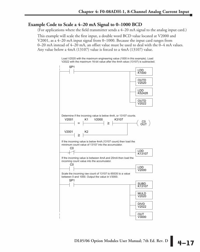
DL05/06 Option Modules User Manual; 7th Ed. Rev. D 4–17
Chapter 4: F0-08ADH-1, 8-Channel Analog Current Input
Example Code to Scale a 4–20 mA Signal to 0–1000 BCD(For applications where the field transmitter sends a 4–20 mA signal to the analog input card.)
This example will scale the first input, a double word BCD value located at V2000 and V2001, as a 4–20 mA input signal from 0–1000. Because the input card ranges from 0–20 mA instead of 4–20 mA, an offset value must be used to deal with the 0–4 mA values. Any value below a 4mA (13107) value is forced to a 4mA (13107) value.
SP1
OUTDV2020
OUTDV2022
LDDK52428
LDDK1000
≥
C0OUT= ≥
V2001 V2000K1
V2001
K3107
K2
MULDV2020
OUTV3000
DIVDV2022
SUBDK13107
SP1
C0LDDV2000
C0LDDK13107
Load V2020 with the maximum engineering value (1000 in this example). Load V2022 with the maximum 16-bit value after the 4mA value (13107) is subtracted.
If the incoming value is below 4mA (13107 count) then load the minimum count value of 13107 into the accumulator.
If the incoming value is between 4mA and 20mA then load the incoming count value into the accumulator.
Determine if the incoming value is below 4mA, or 13107 counts.
Scale the incoming raw count of 13107 to 65535 to a value between 0 and 1000. Output the value in V3000.

DL05/06 Option Modules User Manual; 7th Ed. Rev. D4–18
Chapter 4: F0-08ADH-1, 8-Channel Analog Current Input
Example Code to Scale a 4–20 mA Signal to 0–1000 Binary(For applications where the field transmitter sends a 4–20 mA signal to the analog input card.)
This example will scale the first input, a binary/decimal value located at V2000 (the CPU reserves two words for each channel so V2000 and V2001 are reserved), as a 4–20 mA input signal from 0–1000. Because the input card ranges from 0–20 mA instead of 4–20 mA, an offset value must be used to deal with the 0–4 mA values. Any value below a 4mA (13107 or 3333h) value is forced to a 4mA (13107 or 3333h) value.
SP1
OUTDV2020
OUTDV2022
LDDK52428
LDDK1000
≥
V2000 K3333
V2000 K3333
MULBV2020
OUTV3000
DIVBV2022
SUBBK3333
SP1
LDDV2000
LDDK3333
BIN
BIN
<
If the incoming value is below 4mA (13107 or 3333h) then load the minimum count value of 13107 (3333h) into the accumulator.
If the incoming value is between 4mA and 20mA then load the incoming count value into the accumulator.
Load V2020 with the maximum engineering value (1000 or 3E8h in this example). Load V2022 with the maximum 16-bit value after the 4mA value (13107 or 3333h) is subtracted.
Scale the incoming raw count of 13107 (3333h) to 65535 (FFFFh) to a value between 0 and 1000 (3E8h). Output the value in V3000 as a binary/decimal number.
555F0-04AD-2, 4-ChAnnel AnAlog VoltAge Input
ChapterChapterChapter
In This Chapter...Module Specifications ...............................................................................................5–2
Setting the Module Jumpers .....................................................................................5–4
Connecting and Disconnecting the Field Wiring .....................................................5–5
Wiring Diagram .........................................................................................................5–5
Module Operation .....................................................................................................5–6
Special V-memory Locations .....................................................................................5–7
Using the Pointer in Your Control Program .............................................................5–9
Scale Conversions ....................................................................................................5–11
Module Resolution ...................................................................................................5–14
Analog Input Ladder Logic Filter ............................................................................5–15
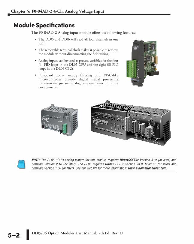
DL05/06 Option Modules User Manual; 7th Ed. Rev. D5–2
Chapter 5: F0-04AD-2 4-Ch. Analog Voltage Input
Module SpecificationsThe F0-04AD-2 Analog input module offers the following features:
• The DL05 and DL06 will read all four channels in one scan.
• The removable terminal block makes it possible to remove the module without disconnecting the field wiring.
• Analog inputs can be used as process variables for the four (4) PID loops in the DL05 CPU and the eight (8) PID loops in the DL06 CPUs.
• On-board active analog filtering and RISC-like microcontroller provide digital signal processing to maintain precise analog measurements in noisy environments.
NOTE: The DL05 CPU’s analog feature for this module requires DirectSOFT32 Version 3.0c (or later) and firmware version 2.10 (or later). The DL06 requires DirectSOFT32 version V4.0, build 16 (or later) and firmware version 1.00 (or later). See our website for more information: www.automationdirect.com.

DL05/06 Option Modules User Manual; 7th Ed. Rev. D 5–3
Chapter 5: F0-04AD-2 4-Ch. Analog Voltage Input
The following tables provide the specifications for the F0–04AD–2 Analog Input Module. Review these specifications to make sure the module meets your application requirements.
Input SpecificationsNumber of Channels 4, single ended (one common)Input Range 0 to 5VDC or 0 to 10VDC (jumper selectable)Resolution 12 bit (1 in 4096)Step Response 10.0 ms to 95% of full step changeCrosstalk -80dB, 1/2 count maximum*Active Low-pass Filtering -3dB at 300Hz (-12dB per octave)Input Impedance Greater than 20kqAbsolute Maximum Ratings ±15VLinearity Error (End to End) ±2 counts maximum*Input Stability ±1 count *Gain Error ±6 counts maximum *Offset Error ±2 counts maximum*
Maximum Inaccuracy±0.3% @ 25°C (77°F)±0.6% 0 to 60°C (32 to 140°F)
Accuracy vs. Temperature ±100ppm /°C typical* One count in the specification tables is equal to one least significant bit of the analog data value (1 in 4096).
General SpecificationsPLC Update Rate 4 input channels per scan16-bit Data Word 12 binary data bitsOperating Temperature 0 to 60° C (32 to 140° F)Storage Temperature -20 to 70° C (-4 to 158° F)Relative Humidity 5 to 95% (non-condensing)Environmental Air No corrosive gases permittedVibration MIL STD 810C 514.2Shock MIL STD 810C 516.2Noise Immunity NEMA ICS3-304Power Budget Requirement 75mA @ 5 VDC (supplied by base)Connector Phoenix Mecano, Inc. Part No. AK1550/8-3.5 - greenConnector Wire Size 28–16 AWGConnector Screw Torque 0.4 N·mConnector Screwdriver Size DN-SS1 (recommended)

DL05/06 Option Modules User Manual; 7th Ed. Rev. D5–4
Chapter 5: F0-04AD-2 4-Ch. Analog Voltage Input
Setting the Module JumpersThe position of the J2 jumpers determines the input signal levels. You can choose between 0–5 VDC or 0–10 VDC. The module ships with the jumpers installed connecting the pins. In this position, the input signal level is 0–5 VDC. To select 0–10 VDC signals, use the jumper selection chart located on the module. One or more channels can be selected for 0–10 VDC input signal level by removing the jumper from the connecting pin of the appropriate channel. This allows you to have some channels selected for 0–5 VDC signals and other channels selected for 0–10 VDC signals.
WARNING: Before removing the analog module or the terminal block on the face of the module, disconnect power to the PLC and all field devices. Failure to disconnect power can result in damage to the PLC and/or field devices.
CH
1C
H2
C14
CH
3C
H4
INP
UT
S
ON=0–5V
RANGE
J2
J2 jumpers shown below areconfigured as CH1 and CH4 setfor 0–10V, and CH2 and CH3set for 0–5V.
Refer to jumper selection chart.

DL05/06 Option Modules User Manual; 7th Ed. Rev. D 5–5
Chapter 5: F0-04AD-2 4-Ch. Analog Voltage Input
Connecting and Disconnecting the Field WiringWiring Guidelines
Your company may have guidelines for wiring and cable installation. If so, you should check those before you begin the installation. Here are some general things to consider:
• Use the shortest wiring route whenever possible.
• Use shielded wiring and ground the shield at the transmitter source. Do not ground the shield at both the module and the source.
• Do not run the signal wiring next to large motors, high current switches, or transformers. This may cause noise problems.
• Route the wiring through an approved cable housing to minimize the risk of accidental damage. Check local and national codes to choose the correct method for your application.
A separate transmitter power supply may be required, depending on the type of transmitter being used.
This module has a removable connector to make wiring and module removal easier. To remove the terminal block, disconnect power to the PLC and the field devices. Pull the terminal block firmly until the connector separates from the module.
The analog module can be removed from the PLC by folding out the retaining tabs at the top and bottom of the module. As the retaining tabs pivot upward and outward, the module’s connector is lifted out of the PLC socket. Once the connector is free, you can lift the module out of its slot.
Wiring DiagramUse the following diagram to connect the field wiring. If necessary, the terminal block can be removed to make removal of the module possible without disturbing field wiring.
NOTE 3: To ensure that readings on unused channels are zero, installa jumper between the CHx and COM terminals on all unused channels.
A n a lo g Input
0–10V0–5V
F0–04AD–2
CH1+
CH3+
CH4+
CH2+
0V
0V
0V
0V
4-CHANNELS

DL05/06 Option Modules User Manual; 7th Ed. Rev. D5–6
Chapter 5: F0-04AD-2 4-Ch. Analog Voltage Input
Module OperationInput Channel Update Sequence
The DL05 and DL06 read four channels of input data during each scan. The CPU supports special V-memory locations that are used to manage the data transfer. This is discussed in more detail on the next page, “Special V-memory Locations”.
Analog Module UpdatesEven though the channel updates to the CPU are synchronous with the CPU scan, the module asynchronously monitors the analog transmitter signals and converts each signal into a 12-bit binary representation. This enables the module to continuously provide accurate measurements without slowing down the discrete control logic in the RLL program.
The module takes approximately 10 milliseconds to sense 95% of the change in the analog signal. For the vast majority of applications, the process changes are much slower than these updates.
NOTE: If you are comparing other manufacturers’ update times (step responses) with ours, please be aware that some manufacturers refer to the time it takes to convert the analog signal to a digital value. Our analog to digital conversion takes only a few microseconds. It is the settling time of the filter that is critical in determining the full update time. Our update time specification includes the filter settling time.
Read the data
Store data
Read Inputs
Execute Application Program
Scan
Write to Outputs
Ch 1, 2, 3, 4Scan N
Scan N+1
Scan N+2
Scan N+3
Scan N+4
Ch 1, 2, 3, 4
Ch 1, 2, 3, 4
Ch 1, 2, 3, 4
Ch 1, 2, 3, 4
DL05/DL06 PLC

DL05/06 Option Modules User Manual; 7th Ed. Rev. D 5–7
Chapter 5: F0-04AD-2 4-Ch. Analog Voltage Input
Special V-memory LocationsFormatting the Module Data
The DL05 and DL06 PLCs have special V-memory locations assigned to their respective option slots. These V-memory locations allow you to:
• Specify the data format (binary or BCD)
• Specify the number of channels to scan (4 channels for the F0-04AD-2)
• Specify the V-memory locations to store the input data
DL05 Data FormattingThe table below shows the special V-memory locations which are used by the DL05 PLC for the F0–04AD–2.
Structure of V7700Special V-memory location 7700 identifies that a F0-04AD-2 module is installed in the DL05 option slot and the data type to be either binary or BCD.
Loading a constant of 400 into V7700 identifies a 4 channel analog input module is installed in the DL05 option slot, and reads the input data values as BCD numbers.
Loading a constant of 8400 into V7700 identifies a 4 channel analog input module is installed in the DL05 option slot, and reads the input data values as binary numbers.
Structure of V7701V7701 is a system V-memory location used as a pointer to a user V-memory location where the analog input data is stored. The V-memory location loaded into V7701 is an octal number identifying the first user V-memory location for reading the analog input data. This V-memory location is user selectable. For example, loading O2000 causes the pointer to write Ch 1’s data value to V2000, Ch 2’s data value to V2001, Ch 3’s data value to V2002, and Ch 4’s data value to V2003.
You will find an example program that loads appropriate values to V7700 and V7701 on page 5–9.
Analog Input Module DL05 Special V-memory Locations
Data Type and Number of I/O Channels V7700Input Storage Pointer V7701
MSB LSB
15
014
13
12
11
10
9 8 7 6 5 4 3 2 1
MSB LSB
15
014
13
12
11
10
9 8 7 6 5 4 3 2 1

DL05/06 Option Modules User Manual; 7th Ed. Rev. D5–8
Chapter 5: F0-04AD-2 4-Ch. Analog Voltage Input
DL06 Data FormattingSpecial V-memory locations are assigned to the four option module slots of the DL06 PLC. The table below shows these V-memory locations which can be used for the F0–04AD–2.
Setup Data Type and Number of ChannelsV-memory locations 700, 710, 720 and 730 are used to set the data format to be read in either binary or BCD, and to set the number of channels that will be active.
For example, the F0–04AD–2 is installed in slot 1. Loading a constant of 400 into V700 sets 4 channels active, and the input data value is read as a BCD number.
With the F0–4AD–2 in slot 1, loading a constant of 8400 into V700 sets 4 channels active, and the input data value is read as a binary number.
Storage Pointer SetupV-memory locations 701, 711, 721 and 731 are special locations used as storage pointers for the analog input data. With the analog module installed in slot 4, the V-memory location loaded in V731, for instance, is an octal number identifying the first user V-memory location to read the analog input data. This V-memory location is user selectable. For example, loading O2000 using the LDA instruction causes the pointer to write Ch 1’s data value to V2000, Ch 2’s data value to V2001, CH 3’s data value to V2002 and Ch 4’s data value to V2003.
You will find an example program that loads appropriate values to V700 and V701 on page 5–10.
Analog Input Module DL06 Special V-memory Locations
Slot No. 1 2 3 4Number of Channels V700 V710 V720 V730Input Pointer V701 V711 V721 V731
MSB LSB
15
014
13
12
11
10
9 8 7 6 5 4 3 2 1
MSB LSB
15
014
13
12
11
10
9 8 7 6 5 4 3 2 1

DL05/06 Option Modules User Manual; 7th Ed. Rev. D 5–9
Chapter 5: F0-04AD-2 4-Ch. Analog Voltage Input
Using the Pointer in Your Control ProgramDL05 Pointer Method
The DL05 CPU examines the pointer values (the memory locations identified in V7700 and V7701) on the first scan only.
The example program below shows how to setup these locations. This rung can be placed anywhere in the ladder program or in the initial stage if you are using stage programming instructions.
This is all that is required to read the analog input data into V-memory locations. Once the data is in V-memory you can perform math on the data, compare the data against preset values, and so forth. V2000 is used in the example but you can use any user V-memory location.
SP0LD
LDAO2000
OUTV7701
This loads an octal value for the first V-memory location that will be usedto store the incoming data. For example, the O2000 entered here woulddesignate the following addresses.Ch1 – V2000, Ch2 – V2001, Ch3 – V2002, Ch 4 – V2003The octal address (O2000) is stored here. V7701 is assigned to theoption slot and acts as a pointer, which means the CPU will use the octalvalue in this location to determine exactly where to store the incomingdata.
OUTV7700
Special V-memory location assigned to the option slot contains the dataformat and the number of channels to scan.
Loads a constant that specifies the number of channels to scan and thedata format. The upper byte selects the data format (i.e. 0=BCD,8=Binary) and the number of channels (set to 4 for the F0–04AD–2).
- or -The binary format is used for displaying data on some operatorinterface units. The DL05 PLCs support binary math functions.
K400
K8400LD

DL05/06 Option Modules User Manual; 7th Ed. Rev. D5–10
Chapter 5: F0-04AD-2 4-Ch. Analog Voltage Input
DL06 Pointer MethodUse the special V-memory table below as a guide to setup the pointer values in the following example for the DL06. Slot 1 is the left most option slot. The CPU will examine the pointer values at these locations only after a mode transition, first scan only.
The F0–04AD–2 can be installed in any available DL06 option slot. Using the example program from the previous page, but changing the V-memory addresses, the ladder diagram below shows how to setup these locations with the module installed in slot 1 of the DL06. Use the above table to determine the pointer values if locating the module in any of the other slot locations. Place this rung anywhere in the ladder program or in the initial stage if you are using stage programming instructions.
Like the DL05 example, this logic is all that is required to read the analog input data into V-memory locations. Once the data is in V-memory you can perform mathematical calculations with the data, compare the data against preset values, and so forth. V2000 is used in the example but you can use any user V-memory location.
SP0LD
LDAO2000
OUTV701
This loads an octal value for the first V-memory location that will be usedto store the incoming data. For example, the O2000 entered here woulddesignate the following addresses.Ch1 – V2000, Ch2 – V2001, Ch3 – V2002, Ch 4 – V2003
The octal address (O2000) is stored here. V701 is assigned to thefirst option slot and acts as a pointer, which means the CPU will usethe octal value in this location to determine exactly where to store theincoming data.
OUTV700
Special V-memory location assigned to the first option slot contains thedata format and the number of channels to scan.
Loads a constant that specifies the number of channels to scan and thedata format. The upper byte selects the data format (i.e. 0=BCD,8=Binary) and the number of channels (set to 4 for the F0–04AD–2).
- or -The binary format can be used for displaying data on someoperator interface units and the DL06 LCD display. The DL06PLCs support binary math functions.
K400
K8400LD
Analog Input Module DL06 Special V-memory Locations
Slot No. 1 2 3 4Number of Channels V700 V710 V720 V730Input Pointer V701 V711 V721 V731

DL05/06 Option Modules User Manual; 7th Ed. Rev. D 5–11
Chapter 5: F0-04AD-2 4-Ch. Analog Voltage Input
Scale ConversionsScaling the Input Data
Many applications call for measurements in engineering units, which can be more meaningful than raw data. Convert to engineering units using the formula shown to the right.
You may have to make adjustments to the formula depending on the scale you choose for the engineering units.
For example, if you wanted to measure pressure (PSI) from 0.0 to 100.0 then you would have to multiply the analog value by 10 in order to imply a decimal place when you view the value with the programming software or a handheld programmer. Notice how the calculations differ when you use the multiplier.
Analog Value of 2024, slightly less than half scale, should yield 49.4 PSI
Units = A H – L4095
H = High limit of the engineeringunit range
L = Low limit of the engineering unit range
A = Analog value (0 – 4095)
+ L
Units = A H – L4095
Example without multiplier Example with multiplier
Units = 2024 100 – 04095
Units = 49
Units = 10 A H – L 4095
Units = 20240 100 – 0 4095
Units = 494
+ L
+ 0
+ L
+ 0

DL05/06 Option Modules User Manual; 7th Ed. Rev. D5–12
Chapter 5: F0-04AD-2 4-Ch. Analog Voltage Input
The Conversion Program
The following example shows how you would write the program to perform the engineering unit conversion from input data formats 0–4095. This example assumes the raw input data read at V2000 is in BCD format.
Note: this example uses SP1, which is always on. You could also use an X, C, etc., permissive contact.
LDV2000
SP1
MULK1000
DIVK4095
When SP1 is on, load channel 1 data to the accumulator (fora range of 0–1000).
Multiply the accumulator by 1000.
Divide the accumulator by 4095 (the module resolution).
OUTV2100
Store the result in V2100.

DL05/06 Option Modules User Manual; 7th Ed. Rev. D 5–13
Chapter 5: F0-04AD-2 4-Ch. Analog Voltage Input
Analog and Digital Value ConversionsSometimes it is useful to convert between the signal levels and the digital values. This is especially helpful during machine startup or troubleshooting. The following table provides formulas to make this conversion easier.
For example, if you are using the 0–10 V range and you need a 6V signal level, use this formula to determine the digital value (D) that will be stored in the V-memory location that contains the data.
D = 409510
(A)
D = 409510
(6V)
D = (409.5) (6) D = 2457
Range If you know the digital value If you know the analog signal level
0 to 5V A = 5D 4095
D = 4095 (A) 5
0 to 10V A = 10D 4095
D = 4095 (A) 10

DL05/06 Option Modules User Manual; 7th Ed. Rev. D5–14
Chapter 5: F0-04AD-2 4-Ch. Analog Voltage Input
Module ResolutionAnalog Data Bits
The first twelve bits represent the analog data in binary format.
Resolution DetailsSince the module has 12-bit resolution, the analog voltage signal is converted into 4096 counts ranging from 0–4095 (212). For example, with a 0 to 10V range, a 0V signal would be a count value of 0, and a 10V signal would produce a count value of 4095. This is equivalent to a binary value of 0000 0000 0000 to 1111 1111 1111, or 000 to FFF hexadecimal.
Each count can also be expressed in terms of the signal level by using the following equation:
The following table shows the smallest detectable signal change that will result in one LSB change in the data value for each increment of the signal change.
10V
0V0 4095
0 – 10VResolution = H – L
4095
H = high limit of the signal range
L = low limit of the signal range
Voltage Range Signal Span (H – L) Divide By Smallest Detectable
Change0 to 5V 5 volts 4095 1.22 mV0 to 10V 10 volts 4095 2.44 mV
Bit Value Bit Value0 1 6 641 2 7 1282 4 8 2563 8 9 5124 16 10 10245 32 11 2048
MSB LSB
011
10
9 8 7 6 5 4 3 2 1
= data bits

DL05/06 Option Modules User Manual; 7th Ed. Rev. D 5–15
Chapter 5: F0-04AD-2 4-Ch. Analog Voltage Input
Analog Input Ladder Logic FilterPID Loops / Filtering:
Please refer to the “PID Loop Operation” chapter in the DL06 or DL05 User Manual for information on the built-in PV filter (DL05/06) and the ladder logic filter (DL06 only) shown below. A filter must be used to smooth the analog input value when auto tuning PID loops to prevent giving a false indication of loop characteristics.
Smoothing the Input Signal (DL06 only):The filter logic can also be used in the same way to smooth the analog input signal to help stabilize PID loop operation or to stabilize the analog input signal value for use with an operator interface display, etc.
WARNING: The built-in and logic filters are not intended to smooth or filter noise generated by improper field device wiring or grounding. Small amounts of electrical noise can cause the input signal to bounce considerably. Proper field device wiring and grounding must be done before attempting to use the filters to smooth the analog input signal.
Using Binary Data Format
LDDV2000
SUBRV1400
BTOR
SP1Loads the analog signal, which is in binary formatand has been loaded from V–memory locationV2000 – 2001, into the accumulator. Contact SP1is always on.
OUTDV1400
ADDRV1400
MULRR0.2
OUTV2100
RTOB
Converts the binary value in the accumulatorto a real number.
Subtracts the real number stored in locationV1400 from the real number in the accumulator,and stores the result in the accumulator. V1400is the designated workspace in this example.
Multiplies the real number in the accumulator by0.2 (the filter factor), and stores the result in the accumulator. This is the filtered value. The filterrange is 0.1 to 0.9. Smaller filter factorsincrease filtering. (1.0 eliminates filtering.)
Adds the real number stored in location V1400 to the real number filtered value in the accumulator, and stores the result in the accumulator.
Copies the value in the accumulator tolocation V1400.
Converts the real number in theaccumulator to a binary value, andstores the result in the accumulator.
Loads the binary number filtered value fromthe accumulator into location V2100 to use inyour application or PID loop.

DL05/06 Option Modules User Manual; 7th Ed. Rev. D5–16
Chapter 5: F0-04AD-2 4-Ch. Analog Voltage Input
NOTE: Be careful not to do a multiple number conversion on a value. For example, if you are using the pointer method in BCD format to get the analog value, it must be converted to binary (BIN) as shown below. If you are using the pointer method in Binary format, the conversion to binary (BIN) instruction is not needed.
Using BCD Data Format
LDV2000
SUBRV1400
BTOR
SP1
BIN
OUTDV1400
ADDRV1400
MULRR0.2
OUTV1402
BCD
RTOB
Loads the analog signal, which is in BCD formatand has been loaded from V–memory locationV2000, into the accumulator. Contact SP1is always on.
Converts the BCD value in the accumulatorto binary.
Subtracts the real number stored in locationV1400 from the real number in the accumulator,and stores the result in the accumulator. V1400is the designated workspace in this example.
Multiplies the real number in the accumulator by0.2 (the filter factor), and stores the result in the accumulator. This is the filtered value. The filterrange is 0.1 to 0.9. Smaller filter factorsincrease filtering. (1.0 eliminates filtering.)
Adds the real number stored in location V1400 to the real number filtered value in the accumulator, and stores the result in the accumulator.
Copies the value in the accumulator tolocation V1400.
Converts the real number in theaccumulator to a binary value, andstores the result in the accumulator.
Loads the BCD number filtered value fromthe accumulator into location V1402 to use inyour application or PID loop.
Converts the binary value in the accumulator to a real number.
Converts the binary value in the accumulatorto a BCD number. Note: The BCD instruction is not needed to PID loop PV (loop PV is a binary number).
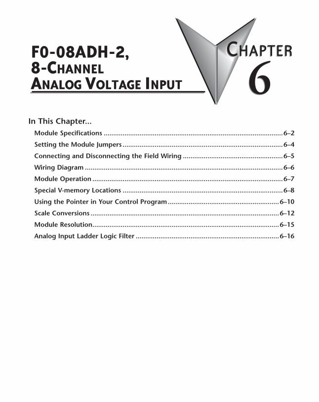
F0-08ADH-2, 8-CHAnnel AnAlog VoltAge Input 666
ChapterChapterChapter
In This Chapter...Module Specifications ...............................................................................................6–2
Setting the Module Jumpers .....................................................................................6–4
Connecting and Disconnecting the Field Wiring .....................................................6–5
Wiring Diagram .........................................................................................................6–6
Module Operation .....................................................................................................6–7
Special V-memory Locations .....................................................................................6–8
Using the Pointer in Your Control Program ...........................................................6–10
Scale Conversions ....................................................................................................6–12
Module Resolution ...................................................................................................6–15
Analog Input Ladder Logic Filter ............................................................................6–16

DL05/06 Option Modules User Manual; 7th Ed. Rev. D6–2
Chapter 6: F0-08ADH-2, 8-Channel Analog Voltage Input
Module SpecificationsThe F0-08ADH-2 Analog Input module offers the following features:
• The DL05 and DL06 will read all eight channels in one scan.
• The removable terminal block simplifies module replacement.
• Analog inputs can be used as process variables for the four (4) PID loops in the DL05 and the eight (8) PID loops in the DL06 CPUs.
• On-board active analog filtering and RISC-like microcontroller provide digital signal processing to maintain precise analog measurements in noisy environments.
NOTE: The DL05 CPU’s analog feature for this module requires DirectSOFT32 Version 3.0c (or later) and firmware version 5.20 (or later). The DL06 requires DirectSOFT32 version V4.0, build 16 (or later) and firmware version 2.30 (or later). See our website for more information: www.automationdirect.com.

DL05/06 Option Modules User Manual; 7th Ed. Rev. D 6–3
Chapter 6: F0-08ADH-2, 8-Channel Analog Voltage Input
The following tables provide the specifications for the F0–08ADH–2 Analog Input Module. Review these specifications to make sure the module meets your application requirements.
Input SpecificationsInputs per module 8Input Range 0–5 VDC or 0–10 VDC (Jumper selectable)Resolution 16-bit, 76µV /bit or 152µV /bitInput Type Single Ended (one common)Maximum Continuous Overload ±100VInput Impedance >200kΩFilter Characteristics Low pass, -3dB @ 60HzPLC Data Format 16-bit, Unsigned Integer, 0–FFFF (binary) or 0–65535 (BCD)*
Sample Duration Time 10.2 msAll Channel Update Rate 81.6 msConversion Method Successive ApproximationAccuracy vs. Temperature ±50PPM / °C MaximumMaximum Inaccuracy 0.2% of range (including temperature drift)
Linearity Error (End to End) ±10 count maximum Monotonic with no missing codes
Input Stability and Repeatability ±10 count (after 10 min. warm up)Full Scale Calibration Error (including Offset)
±10 counts maximum
Offset Calibration Error ±10 count maximumMaximum Crosstalk at DC, 50 Hz and 60 Hz ±10 count maximum External 24VDC Power Required 24VDC ±10% @ 25mABase Power Required (5.0V) 25mA
General SpecificationsOperating Temperature 0 to 55°C (32 to 131°F)Storage Temperature -20 to 70°C (-4 to 158°F)Humidity 5 to 95% (non-condensing)Environmental air No corrosive gases permitted (EN61131-2 pollution degree 1)Vibration MIL STD 810C 514.2Shock MIL STD 810C 516.2Field to Logic side Isolation 1800VAC applied for 1 second (100% tested)Insulation Resistance >10M ohms @ 500VDC
Noise ImmunityNEMA ICS3-304; Impulse 1000V @ 1ms pulse; RFI, (145MHz, 440MHz 5W @ 15cm); Worst case error during noise disturbance is 0.5% of full scale
Agency Approvals UL508; UL60079-15 Zone 2Module Location Any slot in a DL05 or DL06 SystemField Wiring Removable Terminal BlockWeight 49g (1.7 oz.)
*Each channel requires 2 words of V-memory irrespective of the format used.

DL05/06 Option Modules User Manual; 7th Ed. Rev. D6–4
Chapter 6: F0-08ADH-2, 8-Channel Analog Voltage Input
Setting the Module JumpersThe position of the jumper determines the input signal voltage levels. You can choose between 0–5 VDC or 0–10 VDC. The 0–5V position is the default position. With the jumper connecting the J5 posts, an input signal level of 0–5 VDC is selected. Select 0–10 VDC inputs by removing the jumper from the J5 posts and placing it across the J4 posts.
FACTSF0-08ADH-2
J4
J5
ON=0–10V
ON=0–5V
J4
J5
J4
J50–5 Volt Operation 0–10 Volt Operation
default jumper position
Setting the appropriate jumper
Locating the jumpers

DL05/06 Option Modules User Manual; 7th Ed. Rev. D 6–5
Chapter 6: F0-08ADH-2, 8-Channel Analog Voltage Input
Connecting and Disconnecting the Field Wiring
WARNING: Before removing the analog module or the terminal block on the face of the module, disconnect power to the PLC and all field devices. Failure to disconnect power can result in damage to the PLC and/or field devices.
Wiring GuidelinesYour company may have guidelines for wiring and cable installation. If so, you should check those before you begin the installation. Here are some general things to consider:
• Use the shortest wiring route whenever possible.
• Use shielded wiring and ground the shield at the transmitter source. Do not ground the shield at both the module and the source.
• Do not run the signal wiring next to large motors, high current switches, or transformers. This may cause noise problems.
• Route the wiring through an approved cable housing to minimize the risk of accidental damage. Check local and national codes to choose the correct method for your application.
The F0–08ADH–2 does not supply power to field devices. You will need to power transmitters separately from the PLC.
To remove the terminal block, disconnect power to the PLC and the field devices. Pull the terminal block firmly until the connector separates from the module.
You can remove the analog module from the PLC by folding out the retaining tabs at the top and bottom of the module. As the retaining tabs pivot upward and outward, the module’s connector is lifted out of the PLC socket. Once the connector is free, you can lift the module out of its slot.
Terminal Block SpecificationsNumber of Positions 13Re-Order Number D0-ACC-4Pitch 0.2 inch (5.08 mm)
Wire Range 28–16AWG Solid or Stranded Conductor; Wire strip length 5/16” (7–8 mm)
Screwdriver Size (Slotted) 0.4T x 2.5W mm (part number DN-SS1)Screw Size M2.5 sizeScrew Torque 4.5 inch-pounds (0.52 N·m)

DL05/06 Option Modules User Manual; 7th Ed. Rev. D6–6
Chapter 6: F0-08ADH-2, 8-Channel Analog Voltage Input
Wiring DiagramUse the following diagram to connect the field wiring. If necessary, the F0–08ADH–2 terminal block can be removed to make removal of the module possible without disturbing field wiring.
ANALOG0–10V
F0-08ADH-2
IN
CH1
CH2
CH3
CH4
COM
CH5
CH6
CH7
CH8
COM
COM
+24V
0V
24VDCPower Supply
0VDC
+24VDC
COM
COM
COM
4-wire VoltageTransmitter
AC or DC CH5
+3-wire VoltageTransmitter
CH3
CH1
CH8
Shield, Ch. 5Voltage Transmitter
Shield, Ch. 8Voltage Transmitter
Note 1: Do not connect both ends of shield.
SHIELD CONNECTED TO SIGNALSOURCE COMMON. SEE NOTE 1.
CH1 ADC
CH2 ADC
CH3 ADC
CH4 ADC
CH5 ADC
CH6 ADC
CH7 ADC
CH8 ADC
0V
Internal Module CircuitryTypical User Wiring
ISOLATED ANALOGCIRCUIT POWER
Voltage TransmitterShield, Ch. 1
+3-wire VoltageTransmitter
Voltage TransmitterShield, Ch. 3
+3-wire VoltageTransmitter
NOTE 2: To ensure that readings on unused channels are zero, installa jumper between the CHx and COM terminals on all unused channels.

DL05/06 Option Modules User Manual; 7th Ed. Rev. D 6–7
Chapter 6: F0-08ADH-2, 8-Channel Analog Voltage Input
Module OperationChannel Scanning Sequence
The DL05 and DL06 will read all eight channels of input data during each scan. Each CPU supports special V-memory locations that are used to manage the data transfer. This is discussed in more detail beginning in the section on “Special V-memory Locations”.
Analog Module UpdatesEven though the channel updates to the CPUs are synchronous with the CPU scan, the module asynchronously monitors the analog transmitter signals and converts each signal into a 16-bit binary representation. This enables the module to continuously provide accurate measurements without slowing down the discrete control logic in the RLL program.
The module takes approximately 10.2 milliseconds to sense 95% of the change in the analog signal per channel. It takes approximately 81.6 ms to sample all channels.
NOTE: If you are comparing other manufacturers’ update times (step responses) with ours, please be aware that some manufacturers refer to the time it takes to convert the analog signal to a digital value. Our analog to digital conversion takes only a few microseconds. It is the settling time of the filter that is critical in determining the full update time. Our update time specification includes the filter settling time.
Read the data
Store data
Read Inputs
Execute Application Program
Scan
Write to Outputs
Scan N
Scan N+1
Scan N+2
Scan N+3
Scan N+4
DL05/DL06 PLC
Ch 1, 2, 3, 4, 5, 6, 7, 8
Ch 1, 2, 3, 4, 5, 6, 7, 8
Ch 1, 2, 3, 4, 5, 6, 7, 8
Ch 1, 2, 3, 4, 5, 6, 7, 8
Ch 1, 2, 3, 4, 5, 6, 7, 8

DL05/06 Option Modules User Manual; 7th Ed. Rev. D6–8
Chapter 6: F0-08ADH-2, 8-Channel Analog Voltage Input
Special V-memory LocationsFormatting the Analog Module Data
The DL05 and DL06 PLCs have special V-memory locations assigned to their respective option slots. These V-memory locations allow you to:
• Specify the data format (binary or BCD)
• Specify the number of channels to scan (up to 8 channels for the F0–08ADH–2)
• Specify the V-memory locations to store the input data
DL05 Data FormattingThe table below shows the special V-memory locations used by the DL05 PLC for the F0–08ADH–2.
Setup Data Type and Number of Active ChannelsV-memory location 7700 is used to set the data format to either BCD or binary and to set the number of channels that will be active.
For example, assume the F0–08ADH–2 is installed in the option slot. Loading a constant of 800 into V7700 sets 8 channels active and causes the input data value to be read as a BCD number.
With the F0–08ADH–2 in the option slot, loading a constant of 8800 into V7700 sets 8 channels active, and the input data value is read as a binary number.
Storage Pointer SetupV7701 is a system V-memory location used as a pointer to a user V-memory location where the analog input data is stored. The V-memory location loaded into V7701 is an octal number identifying the first user V-memory location for reading the analog input data. This V-memory location is user selectable. For example, loading O2000 causes the pointer to write Ch 1’s data value to V2000 – 2001, Ch 2’s data value to V2002 – 2003, Ch 3’s data value to V2004 – 2005, Ch 4’s data value to V2006 – 2007, Ch 5’s data value to V2010 – 2011, Ch 6’s data value to V2012 – 2013, Ch 7’s data value to V2014 – 2015, and Ch 8’s data value to V2016 – 2017.
You will find an example program that loads appropriate values to V7700 and V7701 on page 6–10.
MSB LSB
0115
10
11
12
13
14
789 6 5 4 3 2
MSB LSB
0115
10
11
12
13
14
789 6 5 4 3 2
V7700 BCD setup
V7700 binary setup
Analog Input Module DL05 Special V-memory Locations
Data Type and Number of Channels V7700Storage Pointer V7701
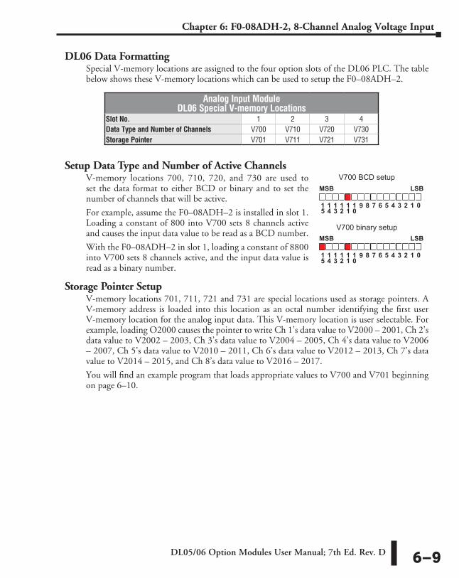
DL05/06 Option Modules User Manual; 7th Ed. Rev. D 6–9
Chapter 6: F0-08ADH-2, 8-Channel Analog Voltage Input
DL06 Data FormattingSpecial V-memory locations are assigned to the four option slots of the DL06 PLC. The table below shows these V-memory locations which can be used to setup the F0–08ADH–2.
Setup Data Type and Number of Active ChannelsV-memory locations 700, 710, 720, and 730 are used to set the data format to either BCD or binary and to set the number of channels that will be active.
For example, assume the F0–08ADH–2 is installed in slot 1. Loading a constant of 800 into V700 sets 8 channels active and causes the input data value to be read as a BCD number.
With the F0–08ADH–2 in slot 1, loading a constant of 8800 into V700 sets 8 channels active, and the input data value is read as a binary number.
Storage Pointer SetupV-memory locations 701, 711, 721 and 731 are special locations used as storage pointers. A V-memory address is loaded into this location as an octal number identifying the first user V-memory location for the analog input data. This V-memory location is user selectable. For example, loading O2000 causes the pointer to write Ch 1’s data value to V2000 – 2001, Ch 2’s data value to V2002 – 2003, Ch 3’s data value to V2004 – 2005, Ch 4’s data value to V2006 – 2007, Ch 5’s data value to V2010 – 2011, Ch 6’s data value to V2012 – 2013, Ch 7’s data value to V2014 – 2015, and Ch 8’s data value to V2016 – 2017.
You will find an example program that loads appropriate values to V700 and V701 beginning on page 6–10.
Analog Input Module DL06 Special V-memory Locations
Slot No. 1 2 3 4Data Type and Number of Channels V700 V710 V720 V730Storage Pointer V701 V711 V721 V731
MSB LSB
0115
10
11
12
13
14
789 6 5 4 3 2
MSB LSB
0115
10
11
12
13
14
789 6 5 4 3 2
V700 BCD setup
V700 binary setup

DL05/06 Option Modules User Manual; 7th Ed. Rev. D6–10
Chapter 6: F0-08ADH-2, 8-Channel Analog Voltage Input
Using the Pointer in Your Control ProgramDL05 Pointer Method Using Conventional Ladder Logic
NOTE: The proper use of the DL05 pointer requires that the V-memory address be written to the special memory location on the first scan only. Use the SP0 bit as a permissive contact when using the code shown below.
The example program below shows how to setup these locations. This rung can be placed anywhere in the ladder program or in the initial stage if you are using stage programming instructions.
This is all that is required to read the analog input data into V-memory locations. Once the data is in V-memory you can perform math on the data, compare the data against preset values, and so forth. V2000 is used in the example but you can use any user V-memory location.
DL05 Pointer Method Using the IBox Instruction Available in DirectSOFT5The following logic accomplishes the same thing as the previous ladder example, but it uses the IBox instruction ANLGIN.
SP0LD
LDAO2000
OUTV7701
Ch1 – V2000-2001, Ch2 – V2002-V2003, Ch3 – V2004-V2005, Ch 4 – V2006-2007Ch 5 – V2010-2011, Ch 6 – V2012-V2013, Ch 7 – V2014-V2015, Ch 8 – V2016-V2017.
OUTV7700
Loads a constant that specifies the number of channels to scan and the data format. The upper byte selects the data format (i.e. 0=BCD, 8=Binary)and the number of channels (up to 8 for the F0-08ADH-2).
- or -
K800
K8800LD The binary format is used for displaying data on some operator
interface units. The DL05 PLCs support binary math functions.
Special V-memory location assigned to the option slot contains thedata format and the number of channels to scan.
This loads an octal value for the first V-memory location that will be usedto store the incoming data. For example, the O2000 entered here woulddesignate the following addresses:
The octal address (O2000) is stored here. V7701 is assigned to the option slot and acts as a pointer, which means the CPU will use the octal value in this location to determine exaclty where to store the incoming data.
Analog Input Module Pointer SetupANLGIN IB-460
Base # (K0 - Local)Slot #Number of Input ChannelsInput Data Format (0 - BCD 1 - BIN)Input Data Address
K0K1K8K0
V2000
No permissive contact or input logicis used with this instruction. This instructionoperates on the first scan only.

DL05/06 Option Modules User Manual; 7th Ed. Rev. D 6–11
Chapter 6: F0-08ADH-2, 8-Channel Analog Voltage Input
DL06 Pointer Method Using Conventional Ladder Logic
NOTE: The proper use of the DL06 pointer requires that the V-memory address be written to the special memory location on the first scan only. Use the SP0 bit as a permissive contact when using the code shown below.
Use the special V-memory table below as a guide to setup the storage pointer in the following example for the DL06. Slot 1 is the left most option slot.
The F0–08ADH–2 can be installed in any available DL06 option slot. The ladder diagram below shows how to set up these locations with the module installed in slot 1 of the DL06. Use the above table to determine the pointer values if locating the module in any of the other slot locations. Place this rung anywhere in the ladder program or in the initial stage if you are using stage programming instructions.
This logic is all that is required to read the analog input data into V-memory locations. Once the data is in V-memory you can perform mathematical calculations with the data, compare the data against preset values, and so forth. In the example, V2000 is used, but you can use any user V-memory location.
Analog Input Module DL06 Special V-memory Locations
Slot No. 1 2 3 4No. of Channels V700 V710 V720 V730Input Pointer V701 V711 V721 V731
SP0LD
LDAO2000
OUTV701
OUTV700
K800
K8800LD
Ch1 – V2000-2001, Ch2 – V2002-V2003, Ch3 – V2004-V2005, Ch 4 – V2006-2007Ch 5 – V2010-2011, Ch 6 – V2012-V2013, Ch 7 – V2014-V2015, Ch 8 – V2016-V2017.
Loads a constant that specifies the number of channels to scan and the data format. The upper byte selects the data format (i.e. 0=BCD, 8=Binary)and the number of channels (up to 8 for the F0-08ADH-2).
The binary format is used for displaying data on some operatorinterface units and the DL06 display. The DL06 PLCs support binary math functions.
Special V-memory location assigned to the first option slot contains thedata format and the number of channels to scan.
This loads an octal value for the first V-memory location that will be usedto store the incoming data. For example, the O2000 entered here woulddesignate the following addresses:
The octal address (O2000) is stored here. V701 is assigned to the first option slot and acts as a pointer, which means the CPU will use the octal value in this location to determine exaclty where to store the incoming data.
- or -

DL05/06 Option Modules User Manual; 7th Ed. Rev. D6–12
Chapter 6: F0-08ADH-2, 8-Channel Analog Voltage Input
DL06 Pointer Method Using the IBox Instruction Available in DirectSOFT5The following logic accomplishes the same thing as the previous ladder example, but it uses the IBox instruction ANLGIN.
Scale ConversionsScaling the Input Data
Many applications call for measurements in engineering units, which can be more meaningful than raw data. Convert to engineering units using the formula shown to the right.
You may have to make adjustments to the formula depending on the scale you choose for the engineering units.
For example, if you wanted to measure pressure (PSI) from 0.0 to 99.9 then you would have to multiply the analog value by 10 in order to imply a decimal place when you view the value with the programming software or a handheld programmer. Notice how the calculations differ when you use the multiplier.
Analog Value of 32375, slightly less than half scale, should yield 49.4 PSI.
Analog Input Module Pointer SetupANLGIN IB-460
Base # (K0 - Local)Slot #Number of Input ChannelsInput Data Format (0 - BCD 1 - BIN)Input Data Address
K0K1K8K0
V2000
No permissive contact or input logicis used with this instruction. This instructionoperates on the first scan only.
Units = A H – L65535
H = High limit of the engineeringunit range
L = Low limit of the engineering unit range
A = Analog value (0 – 65535)
+ L
Units = A H – LExample without multiplier Example with multiplier
Units = 100 – 0
Units = 49
Units = 10 x A H – L65535
Units = 323750 100 – 065535
Units = 494
+ L
+ 0
+ L
+ 0
65535
6553532375

DL05/06 Option Modules User Manual; 7th Ed. Rev. D 6–13
Chapter 6: F0-08ADH-2, 8-Channel Analog Voltage Input
The Conversion Program in Standard Ladder LogicThe following example shows how you would write the program to perform the engineering unit conversion. This example assumes you have BCD data loaded into the appropriate V-memory locations using instructions that apply for the model of CPU you are using.
SP0LDD
LDDK65535
OUTDV3002
OUTDV3000
K100
SP1LDD
DIVDV3002
OUTDV2100
MULDV3000
V2000
Loads the constant 100 to the accumulator.
Copies the constant 100 from the accumulatorto the memory location V3000 and V3001.
Loads the constant 65535 to the accumulator.
Copies the content of V2000 from the accumulatorto the memory location V3002 and V3003.
_First Scan
_On
Loads data from V2000 and V2001.
Multiplies the accumulator value by 100 (previously loaded into V3000 and V3001).
Divides the accumulator value by 65535 (previously loaded into V3002 and V3003).
Copies the content of the accumulator to the memory location V2100 and V2101.
32375
V2000/2001
49
V2100/2101

DL05/06 Option Modules User Manual; 7th Ed. Rev. D6–14
Chapter 6: F0-08ADH-2, 8-Channel Analog Voltage Input
Analog and Digital Value ConversionsSometimes it is useful to convert between the signal levels and the digital values. This is especially helpful during machine start-up or troubleshooting. The following table provides formulas to make this conversion easier.
For example, if you have measured the signal as 6V, you can use the formula to determine the digital value that will be stored in the V-memory location that contains the data.
D =
D =
D = 39321
6553510 A
6553510 6V
Range If you know the digital value If you know the analog signal level
0 to 5V A = . D65535
5D = . A65535
5
0 to 10V A = . D65535
10 D = . A6553510

DL05/06 Option Modules User Manual; 7th Ed. Rev. D 6–15
Chapter 6: F0-08ADH-2, 8-Channel Analog Voltage Input
Module ResolutionAnalog Data Bits
Two 16-bit words are reserved for the analog data whether you are using BCD or binary data formatting. The 16 bits in the low word represent the analog data in binary format.
Resolution DetailsSince the module has 16-bit resolution, the analog signal is converted into 65,536 counts ranging from 0 - 65,535 (216). For example, with a 10V range, a 0V signal would be 0 and a 10V signal would be 65535. This is equivalent to a binary value of 0000 0000 0000 0000 to 1111 1111 1111 1111, or 000 to FFFF hexadecimal.
Each count can also be expressed in terms of the signal level by using the following equation:
The following table shows the smallest detectable signal change that will result in one LSB change in the data value for each increment of the signal change.
mA Range Signal Span (H – L) Divide By Smallest Detectable
Change0 to 5V 5 volts 65535 0.07630 mV
0 to 10V 10 volts 65535 0.15259 mV
0 – 10V
0 65535
0V
10VResolution =
H – L
65535
H = high limit of the signal range
L = low limit of the signal range
MSB LSB
013 2
MSB LSB
013 2
BCD Example
V2000V2001
MSB LSB
0115
10
11
12
13
14
789 6 5 4 3 2
= data bits
MSB LSB
15
10
11
12
13
14
789 6 5 4 013 2
V2000V2001
Binary Example
013 2013 2013 2
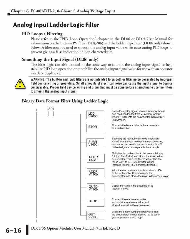
DL05/06 Option Modules User Manual; 7th Ed. Rev. D6–16
Chapter 6: F0-08ADH-2, 8-Channel Analog Voltage Input
Analog Input Ladder Logic FilterPID Loops / Filtering
Please refer to the “PID Loop Operation” chapter in the DL06 or DL05 User Manual for information on the built-in PV filter (DL05/06) and the ladder logic filter (DL06 only) shown below. A filter must be used to smooth the analog input value when auto tuning PID loops to prevent giving a false indication of loop characteristics.
Smoothing the Input Signal (DL06 only) The filter logic can also be used in the same way to smooth the analog input signal to help stabilize PID loop operation or to stabilize the analog input signal value for use with an operator interface display, etc.
WARNING: The built-in and logic filters are not intended to smooth or filter noise generated by improper field device wiring or grounding. Small amounts of electrical noise can cause the input signal to bounce considerably. Proper field device wiring and grounding must be done before attempting to use the filters to smooth the analog input signal.
Binary Data Format Filter Using Ladder Logic
LDDV2000
SUBRV1400
BTOR
SP1Loads the analog signal, which is in binary formatand has been loaded from V–memory locationV2000 – 2001, into the accumulator. Contact SP1is always on.
OUTDV1400
ADDRV1400
MULRR0.2
OUTV2100
RTOB
Converts the binary value in the accumulatorto a real number.
Subtracts the real number stored in locationV1400 from the real number in the accumulator,and stores the result in the accumulator. V1400is the designated workspace in this example.
Multiplies the real number in the accumulator by0.2 (the filter factor), and stores the result in the accumulator. This is the filtered value. The filterrange is 0.1 to 0.9. Smaller filter factorsincrease filtering. (1.0 eliminates filtering.)
Adds the real number stored in location V1400 to the real number filtered value in the accumulator, and stores the result in the accumulator.
Copies the value in the accumulator tolocation V1400.
Converts the real number in theaccumulator to a binary value, andstores the result in the accumulator.
Loads the binary number filtered value fromthe accumulator into location V2100 to use inyour application or PID loop.

DL05/06 Option Modules User Manual; 7th Ed. Rev. D 6–17
Chapter 6: F0-08ADH-2, 8-Channel Analog Voltage Input
NOTE: Be careful not to do a multiple number conversion on a value. For example, if you are using the pointer method in BCD format to get the analog value, it must be converted to binary (BIN) as shown below. If you are using the pointer method in Binary format, the conversion to binary (BIN) instruction is not needed.
Using BCD Data Format
LDDV2000
SUBRV1400
BTOR
SP1
BIN
OUTDV1400
ADDRV1400
MULRR0.2
OUTDV2100
BCD
RTOB
Loads the analog signal, which is in BCD formatand has been loaded from V–memory locationV2000 – 2001, into the accumulator. Contact SP1is always on.
Converts the BCD value in the accumulatorto binary.
Subtracts the real number stored in locationV1400 from the real number in the accumulator,and stores the result in the accumulator. V1400is the designated workspace in this example.
Multiplies the real number in the accumulator by0.2 (the filter factor), and stores the result in the accumulator. This is the filtered value. The filterrange is 0.1 to 0.9. Smaller filter factorsincrease filtering. (1.0 eliminates filtering.)
Adds the real number stored in location V1400 to the real number filtered value in the accumulator, and stores the result in the accumulator.
Copies the value in the accumulator tolocation V1400.
Converts the real number in theaccumulator to a binary value, andstores the result in the accumulator.
Loads the BCD number filtered value fromthe accumulator into location V2100 to use inyour application or PID loop.
Converts the binary value in the accumulator to a real number.
Converts the binary value in the accumulatorto a BCD number. Note: The BCD instruction is not needed to PID loop PV (loop PV is a binary number).

F0-04DAH-1, 4-CHAnnel AnAlog Current output 777
ChapterChapter
In This Chapter...Module Specifications ...............................................................................................7–2
Connecting and Disconnecting the Field Wiring .....................................................7–4
Wiring Diagram .........................................................................................................7–5
Module Operation .....................................................................................................7–6
Special V-memory Locations .....................................................................................7–7
Using the Pointer in Your Control Program .............................................................7–9
Output Scale Conversion .........................................................................................7–11
Module Resolution ...................................................................................................7–14

DL05/06 Option Modules User Manual; 7th Ed. Rev. D7–2
Chapter 7: F0-04DAH-1, 4-Channel Analog Current Output
Module SpecificationsThe F0-04DAH-1 analog output module offers the following features:
• Full 16-bit resolution.
• The DL05 and DL06 will update all four channels in one scan.
• The removable terminal block simplifies module replacement.
NOTE: The DL05 CPU’s analog feature for this module requires DirectSOFT32 Version 3.0c (or later) and firmware version 5.20 (or later). The DL06 requires DirectSOFT32 version V4.0, build 16 (or later) and firmware version 2.30 (or later). See our website for more information: www.automationdirect.com.

DL05/06 Option Modules User Manual; 7th Ed. Rev. D 7–3
Chapter 7: F0-04DAH-1, 4-Channel Analog Current Output
The following tables provide the specifications for the F0–04DAH –1 Analog Output Module. Review these specifications to make sure the module meets your application requirements.
Output SpecificationsOutputs per module 4Output Range 4–20 mAResolution 16-bit, 0.244 µA/bitOutput Type Current sourcing at 20mA max.PLC Data Format 16-bit, Unsigned Integer, 0–FFFF (binary) or 0–65535 (BCD)*
Output value in program mode 4mA (excluding PID, independent mode)Load Impedance 250–750 OhmsMaximum Inductive Load 1mHMaximum Inaccuracy 0.2% of rangeMaximum Full Scale Calibration Error (not including offset error) ±0.025% of range maximum
Maximum Offset Calibration Error ±0.025% of range maximumAccuracy vs. Temperature ±50 ppm/ °C maximum full scale calibration change Maximum Crosstalk ±10 counts
Linearity Error (End to End) ±16 count maximum (±0.025% of full scale) Monotonic with no missing codes
Output Stability and Repeatability ±10 LSB after 10 min. warm-up typicalOutput Ripple 0.05% of Full ScaleOutput Settling Time 0.5 ms maximum, 5µs minimum (full scale change)All Channel Update Rate 100µsMaximum Continuous Overload Outputs open circuit protectedType of Output Protection Electronically current limited to 20mA or lessOutput signal at power-up and power-down 4mAExternal 24VDC Power Required 24VDC ±10% @ 150mABase Power Required (5.0V) 25mA
General SpecificationsOperating Temperature 0 to 55°C (32 to 131°F)Storage Temperature -20 to 70°C (-4 to 158°F)Humidity 5 to 95% (non-condensing)
Environmental air No corrosive gases permitted (EN61131-2 pollution degree 1)
Vibration MIL STD 810C 514.2Shock MIL STD 810C 516.2Field to Logic side Isolation 1800VAC applied for 1 second (100% tested)Insulation Resistance >10M ohms @ 500VDC
Noise ImmunityNEMA ICS3-304; Impulse 1000V @ 1mS pulse; RFI, (145MHz, 440Mhz 5W @ 15cm); Worst case error during noise disturbance is 0.5% of full scale
Agency Approvals UL508; UL60079-15 Zone 2Module Location Any slot in a DL05 or DL06 SystemField Wiring Removable Terminal BlockWeight 49g (1.7 oz.)
*Each channel requires 2 words of V-memory irrespective of the format used.

DL05/06 Option Modules User Manual; 7th Ed. Rev. D7–4
Chapter 7: F0-04DAH-1, 4-Channel Analog Current Output
Connecting and Disconnecting the Field Wiring
WARNING: Before removing the analog module or the terminal block on the face of the module, disconnect power to the PLC and all field devices. Failure to disconnect power can result in damage to the PLC and/or field devices.
Wiring GuidelinesYour company may have guidelines for wiring and cable installation. If so, you should check those before you begin the installation. Here are some general things to consider:
• Use the shortest wiring route whenever possible.
• Use shielded wiring and ground the shield at the transmitter source. Do not ground the shield at both the module and the source.
• Do not run the signal wiring next to large motors, high current switches, or transformers. This may cause noise problems.
• Route the wiring through an approved cable housing to minimize the risk of accidental damage. Check local and national codes to choose the correct method for your application.
The F0–04DAH–1 does not supply power to field devices. You will need to power transmitters separately from the PLC.
To remove the terminal block, disconnect power to the PLC and the field devices. Pull the terminal block firmly until the connector separates from the module.
You can remove the analog module from the PLC by folding out the retaining tabs at the top and bottom of the module. As the retaining tabs pivot upward and outward, the module’s connector is lifted out of the PLC socket. Once the connector is free, you can lift the module out of its slot.
Terminal Block SpecificationsNumber of Positions 13Re-Order Number D0-ACC-4Pitch 0.2 inch (5.08 mm)
Wire Range 28–16AWG Solid or Stranded Conductor; Wire strip length 5/16” (7–8 mm)
Screwdriver Size (Slotted) 0.4T x 2.5W mm (part number DN-SS1)Screw Size M2.5 sizeScrew Torque 4.5 inch-pounds (0.52 N·m)

DL05/06 Option Modules User Manual; 7th Ed. Rev. D 7–5
Chapter 7: F0-04DAH-1, 4-Channel Analog Current Output
Wiring DiagramUse the following diagram to connect the field wiring. If necessary, the F0–04DAH–1 terminal block can be removed to make removal of the module possible without disturbing field wiring.
ANALOG
4–20mA
F0-04DAH-1
OUT
CH1
CH2
CH3
CH4
COM
COM
COM
COM
COM
COM
COM
+24V
0V
24VDCPower Supply
0VDC
+24VDC
COM
CH1
SHIELD CONNECTED TO SIGNALSOURCE COMMON (1 OF 4 SHOWN)
CH1 DAC
CH2 DAC
CH3 DAC
CH4 DAC
ISOLATED ANALOGCIRCUIT COMMON
Internal Module CircuitryTypical User Wiring
CH3
ISOLATED ANALOGCIRCUIT POWER
4–20mA current sourcing
4–20mA current sourcing
4–20mA current sourcing
4–20mA current sourcing
4-20mA OutputCh. 1
4-20mA OutputCh. 3
4-20mA OutputCh. 4
4-20mA OutputCh. 2
CH2
CH4

DL05/06 Option Modules User Manual; 7th Ed. Rev. D7–6
Chapter 7: F0-04DAH-1, 4-Channel Analog Current Output
Module OperationChannel Scanning Sequence
The DL05 and DL06 will write all four channels of output data during each scan. Each CPU supports special V-memory locations that are used to manage the data transfer. This is discussed in more detail beginning in the section on “Special V-memory Locations.”
Read the data
Store data
Read Inputs
Execute Application Program
Scan
Write to Outputs
Scan N
Scan N+1
Scan N+2
Scan N+3
Scan N+4
DL05/DL06 PLC
Ch 1, 2, 3, 4
Ch 1, 2, 3, 4
Ch 1, 2, 3, 4
Ch 1, 2, 3, 4
Ch 1, 2, 3, 4

DL05/06 Option Modules User Manual; 7th Ed. Rev. D 7–7
Chapter 7: F0-04DAH-1, 4-Channel Analog Current Output
Special V-memory LocationsFormatting the Analog Module Data
The DL05 and DL06 PLCs have special V-memory locations assigned to their respective option slots. These V-memory locations allow you to:
• Specify the data format (binary or BCD)
• Specify the number of channels to update (up to 4 channels for the F0–04DAH–1)
• Specify the V-memory locations where the user program will store the output data pending distribution to the output module
DL05 Data FormattingThe table below shows the special V-memory locations used by the DL05 PLC for the F0–04DAH–1.
Data Type and Number of Active Channels SetupSystem memory location V7700 is used to set the data format either to BCD or binary and to set the number of channels that will be active.
For example, loading a constant of 0004 (BCD) into V7700 sets four channels active and causes the output data value to be read from pointer-designated V-memory as a BCD number.
Alternatively, loading a constant of 0084 (BCD) into V7700 sets four channels active and causes the output data value to be read from pointer-designated V-memory as a binary number.
Storage Pointer SetupSystem memory location V7702 is used as a pointer. It points to a user memory location where the analog output data is stored by the user program, pending distribution to the output module. An octal number is loaded to the pointer memory to identify the beginning of a block of user memory where output values are stored.
For example, loading O2100 into V7702 causes the CPU to look for Ch 1’s output data value in V2100 – 2101, Ch 2’s data value in V2102 – 2103, Ch 3’s data value in V2104 – 2105, and Ch 4’s data value in V2106 – 2107.
You will find an example program that loads appropriate values to V7700 and V7702 on page 7–9.
Analog Output Module DL05 Special V-memory Locations
Data Type and Number of Channels V7700Storage Pointer V7702
MSB LSB
0115
10
11
12
13
14
789 6 5 4 3 2
MSB LSB
0115
10
11
12
13
14
789 6 5 4 3 2
V7700 BCD setup
V7700 binary setup
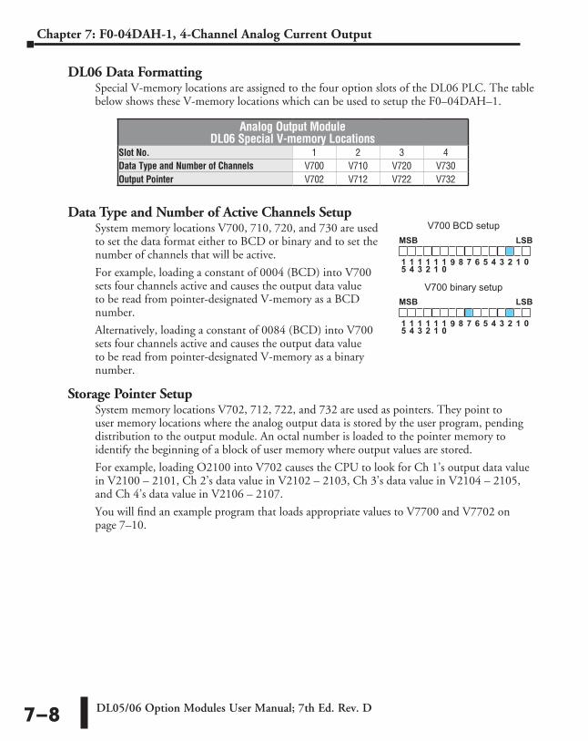
DL05/06 Option Modules User Manual; 7th Ed. Rev. D7–8
Chapter 7: F0-04DAH-1, 4-Channel Analog Current Output
DL06 Data FormattingSpecial V-memory locations are assigned to the four option slots of the DL06 PLC. The table below shows these V-memory locations which can be used to setup the F0–04DAH–1.
Data Type and Number of Active Channels SetupSystem memory locations V700, 710, 720, and 730 are used to set the data format either to BCD or binary and to set the number of channels that will be active.
For example, loading a constant of 0004 (BCD) into V700 sets four channels active and causes the output data value to be read from pointer-designated V-memory as a BCD number.
Alternatively, loading a constant of 0084 (BCD) into V700 sets four channels active and causes the output data value to be read from pointer-designated V-memory as a binary number.
Storage Pointer SetupSystem memory locations V702, 712, 722, and 732 are used as pointers. They point to user memory locations where the analog output data is stored by the user program, pending distribution to the output module. An octal number is loaded to the pointer memory to identify the beginning of a block of user memory where output values are stored.
For example, loading O2100 into V702 causes the CPU to look for Ch 1’s output data value in V2100 – 2101, Ch 2’s data value in V2102 – 2103, Ch 3’s data value in V2104 – 2105, and Ch 4’s data value in V2106 – 2107.
You will find an example program that loads appropriate values to V7700 and V7702 on page 7–10.
Analog Output Module DL06 Special V-memory Locations
Slot No. 1 2 3 4Data Type and Number of Channels V700 V710 V720 V730Output Pointer V702 V712 V722 V732
MSB LSB
0115
10
11
12
13
14
789 6 5 4 3 2
MSB LSB
0115
10
11
12
13
14
789 6 5 4 3 2
V700 BCD setup
V700 binary setup
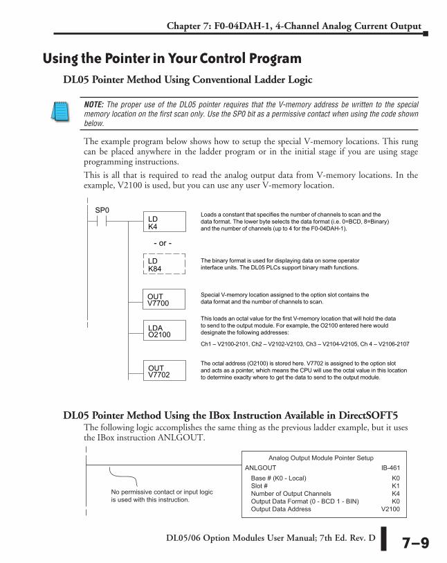
DL05/06 Option Modules User Manual; 7th Ed. Rev. D 7–9
Chapter 7: F0-04DAH-1, 4-Channel Analog Current Output
Using the Pointer in Your Control ProgramDL05 Pointer Method Using Conventional Ladder Logic
NOTE: The proper use of the DL05 pointer requires that the V-memory address be written to the special memory location on the first scan only. Use the SP0 bit as a permissive contact when using the code shown below.
The example program below shows how to setup the special V-memory locations. This rung can be placed anywhere in the ladder program or in the initial stage if you are using stage programming instructions.
This is all that is required to read the analog output data from V-memory locations. In the example, V2100 is used, but you can use any user V-memory location.
DL05 Pointer Method Using the IBox Instruction Available in DirectSOFT5The following logic accomplishes the same thing as the previous ladder example, but it uses the IBox instruction ANLGOUT.
SP0LD
LDAO2100
OUTV7702
Ch1 – V2100-2101, Ch2 – V2102-V2103, Ch3 – V2104-V2105, Ch 4 – V2106-2107
OUTV7700
Loads a constant that specifies the number of channels to scan and the data format. The lower byte selects the data format (i.e. 0=BCD, 8=Binary)and the number of channels (up to 4 for the F0-04DAH-1).
- or -
K4
K84LD The binary format is used for displaying data on some operator
interface units. The DL05 PLCs support binary math functions.
Special V-memory location assigned to the option slot contains thedata format and the number of channels to scan.
This loads an octal value for the first V-memory location that will hold the datato send to the output module. For example, the O2100 entered here woulddesignate the following addresses:
The octal address (O2100) is stored here. V7702 is assigned to the option slot and acts as a pointer, which means the CPU will use the octal value in this location to determine exaclty where to get the data to send to the output module.
Analog Output Module Pointer SetupANLGOUT IB-461
Base # (K0 - Local)Slot #Number of Output ChannelsOutput Data Format (0 - BCD 1 - BIN)Output Data Address
K0K1K4K0
V2100
No permissive contact or input logicis used with this instruction.

DL05/06 Option Modules User Manual; 7th Ed. Rev. D7–10
Chapter 7: F0-04DAH-1, 4-Channel Analog Current Output
DL06 Pointer Method Using Conventional Ladder Logic
NOTE: The proper use of the DL06 pointer requires that the V-memory address be written to the special memory location on the first scan only. Use the SP0 bit as a permissive contact when using the code shown below.
Use the special V-memory table below as a guide to setup the storage pointer in the following example for the DL06. Slot 1 is the left most option slot.
The F0–04DAH–1 can be installed in any available DL06 option slot. The ladder diagram below shows how to setup these locations with the module installed in slot 1 of the DL06. Use the above table to determine the pointer values if locating the module in any of the other slot locations. Place this rung anywhere in the ladder program or in the initial stage if you are using stage programming instructions.
This logic is all that is required to write the analog output data from V-memory locations. In the example, V2100 is used, but you can use any user V-memory location.
Analog Output Module DL06 Special V-memory Locations
Slot No. 1 2 3 4No. of Channels V700 V710 V720 V730Output Pointer V702 V712 V722 V732
SP0LD
LDAO2100
OUTV702
OUTV700
K4
K84LD
Ch1 – V2100-2101, Ch2 – V2102-V2103, Ch3 – V2104-V2105, Ch 4 – V2106-2107.
Loads a constant that specifies the number of channels to scan and the data format. The lower byte selects the data format (i.e. 0=BCD, 8=Binary)and the number of channels (up to 4 for the F0-04DAH-1).
The binary format is used for displaying data on some operatorinterface units and the DL06 display. The DL06 PLCs support binary math functions.
Special V-memory location assigned to the first option slot contains thedata format and the number of channels to scan.
This loads an octal value for the first V-memory location that will hold the datato send to the output module. For example, the O2100 entered here woulddesignate the following addresses:
The octal address (O2100) is stored here. V702 is assigned to the first option slot and acts as a pointer, which means the CPU will use the octal value in this location to determine exaclty where to get the data to send to the output module.
- or -

DL05/06 Option Modules User Manual; 7th Ed. Rev. D 7–11
Chapter 7: F0-04DAH-1, 4-Channel Analog Current Output
DL06 Pointer Method Using the IBox Instruction Available in DirectSOFT5The following logic accomplishes the same thing as the previous ladder example, but it uses the IBox instruction ANLGOUT.
Output Scale ConversionCalculating the Digital Output Value
Your program has to calculate the digital value to send to the analog output module. Most applications use measurements in engineering units, so it is usually necessary to convert from engineering units to a suitable output value. The conversion to an output value can be accomplished by using the conversion formula shown.
You will need to substitute the engineering units for your scale into the formula to the right.
For example, if you want to output pressure (PSI) between 0.0 and 100.0, you may multiply the pressure value by 10 to store in a V-memory location and eliminate the decimal point. Notice how the calculations differ when you use the multiplier.
The following example demonstrates how to output 49.4 PSI.
Example without multiplier Example with multiplier
A = U – L 65535H – L
A = 32112
A = 49 – 0 65535100 – 0
A = U – L 65535H – L
A = 32374
A = 494 – 0 655351000 – 0
H = High limit of the engineeringunit range
L = Low limit of the engineering unit range
A = Analog value (0 – 65535)
A = U – L 65535H – L
U = Engineering units to output
Analog Output Module Pointer SetupANLGOUT IB-461
Base # (K0 - Local)Slot #Number of Output ChannelsOutput Data Format (0 - BCD 1 - BIN)Output Data Address
K0K1K4K0
V2100
No permissive contact or input logicis used with this instruction.

DL05/06 Option Modules User Manual; 7th Ed. Rev. D7–12
Chapter 7: F0-04DAH-1, 4-Channel Analog Current Output
The Conversion Program in Standard Ladder LogicThe following example shows how you would write the program to perform the engineering unit conversion. This example assumes you have BCD data loaded into the appropriate V-memory locations using instructions that apply for the model of CPU you are using.
SP0LDD
LDDK65535
OUTDV3002
OUTDV3000
K100
SP1LDD
OUTDV2100
V2200
Loads the constant 100 to the accumulator.
Copies the constant 100 from the accumulatorto the memory location V3000 and V3001.
Loads the constant 65535 to the accumulator.
Copies the content from the accumulator to the memory location V3002 and V3003.
_First Scan
_On
Loads data from V2200 and V2201.
Copies the content of the accumulator to the memory location V2100 and V2101.
DIVDV3000
Divides the accumulator value by 100 (previously loaded into V3000 and V3001).
MULDV3002
Multiplies the accumulator value by 65535 (previously loaded into V3002 and V3003).
49
V2200/2201
32112
V2100/2101

DL05/06 Option Modules User Manual; 7th Ed. Rev. D 7–13
Chapter 7: F0-04DAH-1, 4-Channel Analog Current Output
Analog and Digital Value ConversionsSometimes it is useful to convert between the signal levels and the digital values. This is especially helpful during machine startup or troubleshooting. The following table provides formulas to make this conversion easier.
The formulas in the table show the relationship between A, the analog value, and D, the digital value.
For example, if you need a 10mA signal to achieve the desired result, you can use the formula to determine the digital value that should be used.
D =
D =
D = 24576
6553516 (A – 4mA).
6553516 (10mA – 4mA).
Range If you know the digital value If you know the analog signal level
4 to 20 mA A = . D65535
16( ) + 4mA D = . (A – 4mA)6553516

DL05/06 Option Modules User Manual; 7th Ed. Rev. D7–14
Chapter 7: F0-04DAH-1, 4-Channel Analog Current Output
Module ResolutionAnalog Data Bits
Two 16-bit words are reserved for the analog data whether you are using BCD or binary data formatting. The 16 bits in the low word represent the analog data in binary format.
Resolution DetailsSince the module has 16-bit resolution, the analog signal is converted into 65,536 counts ranging from 0 - 65,535 (216). A 4mA signal would be 0 and a 20mA signal would be 65535. This is equivalent to a binary value of 0000 0000 0000 0000 to 1111 1111 1111 1111, or 000 to FFFF hexadecimal.
Each count can also be expressed in terms of the signal level by using the following equation:
The following table shows the smallest detectable signal change that will result in one LSB change in the data value for each increment of the signal change.
mA Range Signal Span (H – L) Divide By Smallest Detectable
Change
4 to 20mA 16mA 65535 0.244 µA
4 – 20mA
0 65535
4mA
20mAResolution =
H – L
65535
H = high limit of the signal range
L = low limit of the signal range
MSB LSB
013 2
MSB LSB
013 2
BCD Example
V2000V2001
MSB LSB
0115
10
11
12
13
14
789 6 5 4 3 2
= data bits
MSB LSB
15
10
11
12
13
14
789 6 5 4 013 2
V2000V2001
Binary Example
013 2013 2013 2

F0-08DAH-1, 8-CHAnnel AnAlog Current output 888
ChapterChapterChapter
In This Chapter...Module Specifications ...............................................................................................8–2
Connecting and Disconnecting the Field Wiring .....................................................8–4
Wiring Diagram .........................................................................................................8–5
Module Operation .....................................................................................................8–6
Special System V-memory Locations .........................................................................8–7
Using the Pointer in Your Control Program .............................................................8–9
Output Scale Conversion .........................................................................................8–11
Module Resolution ...................................................................................................8–14

DL05/06 Option Modules User Manual; 7th Ed. Rev. D8–2
Chapter 8: F0-08DAH-1, 8-Channel Analog Current Output
Module SpecificationsThe F0-08DAH-1 analog output module offers the following features:
• The DL05 and DL06 will update all eight channels in one scan.
• The removable terminal block simplifies module replacement.
• Full 16-bit resolution.
NOTE: The DL05 CPU’s analog feature for this module requires DirectSOFT32 Version 3.0c (or later) and firmware version 5.20 (or later). The DL06 requires DirectSOFT32 version V4.0, build 16 (or later) and firmware version 2.30 (or later). See our website for more information: www.automationdirect.com.

DL05/06 Option Modules User Manual; 7th Ed. Rev. D 8–3
Chapter 8: F0-08DAH-1, 8-Channel Analog Current Output
The following tables provide the specifications for the F0–08DAH –1 Analog Output Module. Review these specifications to make sure the module meets your application requirements.
Output SpecificationsOutputs per module 8Output Range 4–20 mAResolution 16-bit, 0.244 µA/bitOutput Type Current sourcing at 20mA max.PLC Data Format 16-bit, Unsigned Integer, 0–FFFF (binary) or 0–65535 (BCD)*
Output value in program mode 4mA (excluding PID, independent mode)Load Impedance 250–750 Ohms Maximum Inductive Load 1mHMaximum Inaccuracy 0.2% of rangeMaximum Full Scale Calibration Error (not including offset error) ±0.025% of range maximum
Maximum Offset Calibration Error ±0.025% of range maximumAccuracy vs. Temperature ±50ppm / °C maximum full scale calibration change Maximum Crosstalk ±10 counts
Linearity Error (End to End) ±16 count maximum (±0.025% of full scale) Monotonic with no missing codes
Output Stability and Repeatability ±10 counts after 10 min. warm-up typicalOutput Ripple 0.05% of Full ScaleOutput Settling Time 0.5 ms maximum, 5µs minimum (full scale change)All Channel Update Rate 100usMaximum Continuous Overload Outputs open circuit protectedType of Output Protection Electronically current limited to 20mA or lessOutput signal at power-up and power-down 4mAExternal 24VDC Power Required 24VDC ±10% @ 220mABase Power Required (5.0 V) 25mA
General SpecificationsOperating Temperature 0 to 55°C (32 to 131°F)Storage Temperature -20 to 70°C (-4 to 158°F)Humidity 5 to 95% (non-condensing)Environmental air No corrosive gases permitted (EN61131-2 pollution degree 1)Vibration MIL STD 810C 514.2Shock MIL STD 810C 516.2Field to Logic side Isolation 1800VAC applied for 1 second (100% tested)Insulation Resistance >10M ohms @ 500VDC
Noise ImmunityNEMA ICS3-304; Impulse 1000V @ 1mS pulse; RFI, (145MHz, 440Mhz 5W @ 15cm); Worst case error during noise disturbance is 0.5% of full scale
Agency Approvals UL508; UL60079-15 Zone 2Module Location Any slot in a DL05 or DL06 SystemField Wiring Removable Terminal BlockWeight 49g (1.7 oz.)
*Each channel requires 2 words of V-memory irrespective of the format used.

DL05/06 Option Modules User Manual; 7th Ed. Rev. D8–4
Chapter 8: F0-08DAH-1, 8-Channel Analog Current Output
Connecting and Disconnecting the Field WiringWARNING: Before removing the analog module or the terminal block on the face of the module, disconnect power to the PLC and all field devices. Failure to disconnect power can result in damage to the PLC and/or field devices.
Wiring GuidelinesYour company may have guidelines for wiring and cable installation. If so, you should check those before you begin the installation. Here are some general things to consider:
• Use the shortest wiring route whenever possible.
• Use shielded wiring and ground the shield at the transmitter source. Do not ground the shield at both the module and the source.
• Do not run the signal wiring next to large motors, high current switches, or transformers. This may cause noise problems.
• Route the wiring through an approved cable housing to minimize the risk of accidental damage. Check local and national codes to choose the correct method for your application.
The F0–08DAH–1 does not supply power to field devices. You will need to power transmitters separately from the PLC.
To remove the terminal block, disconnect power to the PLC and the field devices. Pull the terminal block firmly until the connector separates from the module.
You can remove the analog module from the PLC by folding out the retaining tabs at the top and bottom of the module. As the retaining tabs pivot upward and outward, the module’s connector is lifted out of the PLC socket. Once the connector is free, you can lift the module out of its slot.
Terminal Block SpecificationsNumber of Positions 13Re-Order Number D0-ACC-4Pitch 0.2 inch (5.08 mm)
Wire Range 28–16 AWG Solid or Stranded Conductor; Wire strip length 5/16” (7–8 mm)
Screwdriver Size (Slotted) 0.4T x 2.5W mm (part number DN-SS1)Screw Size M2.5 sizeScrew Torque 4.5 inch-pounds (0.52 N·m)

DL05/06 Option Modules User Manual; 7th Ed. Rev. D 8–5
Chapter 8: F0-08DAH-1, 8-Channel Analog Current Output
Wiring DiagramUse the following diagram to connect the field wiring. If necessary, the F0–08DAH–1 terminal block can be removed to make removal of the module possible without disturbing field wiring.
ANALOG
4–20mA
F0-08DAH-1
OUT
CH1
CH2
CH3
CH4
COM
CH5
CH6
CH7
CH8
COM
COM
+24V
0V
24VDCPower Supply
0VDC
+24VDC
COM
COM
COM
CH5
CH1
CH8
SHIELD CONNECTED TO SIGNALSOURCE COMMON (1 OF 8 SHOWN)
CH1 DAC
CH2 DAC
CH3 DAC
CH4 DAC
CH5 DAC
CH6 DAC
CH7 DAC
CH8 DAC
0V
Internal Module CircuitryTypical User Wiring
CH3
ISOLATED ANALOGCIRCUIT POWER
4–20mA current sourcing
4–20mA current sourcing
4–20mA current sourcing
4–20mA current sourcing
4–20mA current sourcing
4–20mA current sourcing
4–20mA current sourcing
4–20mA current sourcing
4-20mA OutputCh. 1
4-20mA OutputCh. 8
4-20mA OutputCh. 3
4-20mA OutputCh. 4
4-20mA OutputCh. 5
4-20mA OutputCh. 6
4-20mA OutputCh. 7
4-20mA OutputCh. 2
CH2
CH4
CH7
CH6

DL05/06 Option Modules User Manual; 7th Ed. Rev. D8–6
Chapter 8: F0-08DAH-1, 8-Channel Analog Current Output
Module OperationChannel Scanning Sequence
The DL05 and DL06 will read all eight channels of output data during each scan. Each CPU supports special V-memory locations that are used to manage the data transfer. This is discussed in more detail beginning in the section on “Special V-memory Locations”.
Read the data
Store data
Read Inputs
Execute Application Program
Scan
Write to Outputs
Scan N
Scan N+1
Scan N+2
Scan N+3
Scan N+4
DL05/DL06 PLC
Ch 1, 2, 3, 4, 5, 6, 7, 8
Ch 1, 2, 3, 4, 5, 6, 7, 8
Ch 1, 2, 3, 4, 5, 6, 7, 8
Ch 1, 2, 3, 4, 5, 6, 7, 8
Ch 1, 2, 3, 4, 5, 6, 7, 8

DL05/06 Option Modules User Manual; 7th Ed. Rev. D 8–7
Chapter 8: F0-08DAH-1, 8-Channel Analog Current Output
Special System V-memory LocationsFormatting the Analog Module Data
The DL05 and DL06 PLCs have system V-memory locations assigned to their respective option slots. These V-memory locations allow you to:
• Specify the data format (binary or BCD)
• Specify the number of channels to scan (up to 8 channels for the F0–08DAH–1)
• Specify the V-memory locations where the user program will store the output data pending distribution to the output module
DL05 Data FormattingThe table below shows the system V-memory locations used by the DL05 PLC for the F0–08DAH–1.
Data Type and Number of Active Channels SetupSystem memory location V7700 is used to set the data format either to BCD or binary and to set the number of channels that will be active.
For example, loading a constant of 0008 (BCD) into V7700 sets eight channels active and causes the output data value to be read from pointer-designated V-memory as a BCD number.
Alternatively, loading a constant of 0088 (BCD) into V7700 sets eight channels active and causes the output data value to be read from pointer-designated V-memory as a binary number.
Storage Pointer SetupSystem memory location V7702 is used as a pointer. It points to a user memory location where the analog output data is stored by the user program, pending distribution to the output module. An octal number is loaded to the pointer memory to identify the beginning of a block of user memory where output values are stored.
For example, loading O2100 into V7702 causes the CPU to look for Ch 1’s output data value in V2100 – 2101, Ch 2’s data value in V2102 – 2103, Ch 3’s data value in V2104 – 2105, Ch 4’s data value in V2106 – 2107, Ch 5’s data value in V2110 – 2111, Ch 6’s data value in V2112 – 2113, Ch 7’s data value in V2114 – 2115, and Ch 8’s data value in V2116 – 2117.
You will find an example program that loads appropriate values to V7700 and V7702 on page 8–9.
Analog Output Module DL05 Special V-memory Locations
Data Type and Number of Channels V7700Storage Pointer V7702
MSB LSB
0115
10
11
12
13
14
789 6 5 4 3 2
MSB LSB
0115
10
11
12
13
14
789 6 5 4 3 2
V7700 BCD setup
V7700 binary setup

DL05/06 Option Modules User Manual; 7th Ed. Rev. D8–8
Chapter 8: F0-08DAH-1, 8-Channel Analog Current Output
DL06 Data FormattingSpecial V-memory locations are assigned to the four option slots of the DL06 PLC. The table below shows these V-memory locations which can be used to setup the F0–08DAH–1.
Data Type and Number of Active Channels SetupSystem memory locations V700, 710, 720, and 730 are used to set the data format either to BCD or binary and to set the number of channels that will be active.
For example, loading a constant of 0008 (BCD) into V700 sets eight channels active and causes the output data values to be read from pointer-designated V-memory as a BCD number.
Alternatively, loading a constant of 0088 (BCD) into V700 sets eight channels active and causes the output data value to be read from pointer-designated V-memory as a binary number.
Storage Pointer SetupSystem memory locations V702, 712, 722, and 732 are used as pointers. They point to user memory locations where the analog output data is stored by the user program, pending distribution to the output module. An octal number is loaded to the pointer memory to identify the beginning of a block of user memory where output values are stored.
For example, loading O2100 into V702 causes the CPU to look for Ch 1’s output data value in V2100 – 2101, Ch 2’s data value in V2102 – 2103, Ch 3’s data value in V2104 – 2105, Ch 4’s data value in V2106 – 2107, Ch 5’s data value in V2110 – 2111, Ch 6’s data value in V2112 – 2113, Ch 7’s data value in V2114 – 2115, and Ch 8’s data value in V2116 – 2117.
You will find an example program that loads appropriate values to V700 and V702 on page 8–10.
Analog Output Module DL06 Special V-memory Locations
Slot No. 1 2 3 4Data Type and Number of Channels V700 V710 V720 V730Output Pointer V702 V712 V722 V732
MSB LSB
0115
10
11
12
13
14
789 6 5 4 3 2
MSB LSB
0115
10
11
12
13
14
789 6 5 4 3 2
V700 BCD setup
V700 binary setup

DL05/06 Option Modules User Manual; 7th Ed. Rev. D 8–9
Chapter 8: F0-08DAH-1, 8-Channel Analog Current Output
Using the Pointer in Your Control ProgramDL05 Pointer Method Using Conventional Ladder Logic
NOTE: The proper use of the DL05 pointer requires that the V-memory address be written to the special memory location on the first scan only. Use the SP0 bit as a permissive contact when using the code shown below.
The example program below shows how to setup the special V-memory locations. This rung can be placed anywhere in the ladder program or in the initial stage if you are using stage programming instructions.
This is all that is required to read the analog output data from V-memory locations. In the example, V2100 is used, but you can use any user V-memory location.
DL05 Pointer Method Using the IBox Instruction Available in DirectSOFT6The following logic accomplishes the same thing as the previous ladder example, but it uses the IBox instruction ANLGOUT.
SP0LD
LDAO2100
OUTV7702
Ch1 – V2100-2101, Ch2 – V2102-V2103, Ch3 – V2104-V2105, Ch 4 – V2106-2107Ch 5 – V2110-2111, Ch 6 – V2112-V2113, Ch 7 – V2114-V2115, Ch 8 – V2116-V2117.
OUTV7700
Loads a constant that specifies the number of channels to scan and the data format. The lower byte selects the data format (i.e. 0=BCD, 8=Binary)and the number of channels (set to 8 for the F0-08DAH-1).
- or -
K8
K88LD The binary format is used for displaying data on some operator
interface units. The DL05 PLCs support binary math functions.
Special V-memory location assigned to the option slot contains thedata format and the number of channels to scan.
This loads an octal value for the first V-memory location that will hold the datato send to the output module. For example, the O2100 entered here woulddesignate the following addresses:
The octal address (O2100) is stored here. V7702 is assigned to the option slot and acts as a pointer, which means the CPU will use the octal value in this location to determine exaclty where to get the data to send to the output module.
Analog Output Module Pointer SetupANLGOUT IB-461
Base # (K0 - Local)Slot #Number of Output ChannelsOutput Data Format (0 - BCD 1 - BIN)Output Data Address
K0K1K8K0
V2100
No permissive contact or input logicis used with this instruction.

DL05/06 Option Modules User Manual; 7th Ed. Rev. D8–10
Chapter 8: F0-08DAH-1, 8-Channel Analog Current Output
DL06 Pointer Method Using Conventional Ladder Logic
NOTE: The proper use of the DL06 pointer requires that the V-memory address be written to the special memory location on the first scan only. Use the SP0 bit as a permissive contact when using the code shown below.
Use the special V-memory table below as a guide to setup the storage pointer in the following example for the DL06. Slot 1 is the left most option slot.
The F0–08DAH–1 can be installed in any available DL06 option slot. Using the example program from the previous page, but changing the V-memory addresses, the ladder diagram below shows how to setup these locations with the module installed in slot 1 of the DL06. Use the above table to determine the pointer values if locating the module in any of the other slot locations. Place this rung anywhere in the ladder program or in the initial stage if you are using stage programming instructions.
This logic is all that is required to write the analog output data from V-memory locations. In the example, V2100 is used, but you can use any user V-memory location.
Analog Output Module DL06 Special V-memory Locations
Slot No. 1 2 3 4No. of Channels V700 V710 V720 V730Output Pointer V702 V712 V722 V732
SP0LD
LDAO2100
OUTV702
OUTV700
K8
K88LD
Ch1 – V2100-2101, Ch2 – V2102-V2103, Ch3 – V2104-V2105, Ch 4 – V2106-2107Ch 5 – V2110-2111, Ch 6 – V2112-V2113, Ch 7 – V2114-V2115, Ch 8 – V2116-V2117.
Loads a constant that specifies the number of channels to scan and the data format. The lower byte selects the data format (i.e. 0=BCD, 8=Binary)and the number of channels (up to 8 for the F0-08DAH-1).
The binary format is used for displaying data on some operatorinterface units and the DL06 display. The DL06 PLCs support binary math functions.
Special V-memory location assigned to the first option slot contains thedata format and the number of channels to scan.
This loads an octal value for the first V-memory location that will hold the datato send to the output module. For example, the O2100 entered here woulddesignate the following addresses:
The octal address (O2100) is stored here. V702 is assigned to the first option slot and acts as a pointer, which means the CPU will use the octal value in this location to determine exaclty where to get the data to send to the output module.
- or -

DL05/06 Option Modules User Manual; 7th Ed. Rev. D 8–11
Chapter 8: F0-08DAH-1, 8-Channel Analog Current Output
DL06 Pointer Method Using the IBox Instruction Available in DirectSOFT5The following logic accomplishes the same thing as the previous ladder example, but it uses the IBox instruction ANLGOUT.
Output Scale ConversionCalculating the Digital Output Value
Your program has to calculate the digital value to send to the analog output module. Most applications use measurements in engineering units, so it is usually necessary to convert from engineering units to a suitable output value. The conversion to an output value can be accomplished by using the conversion formula shown.
You will need to substitute the engineering units for your scale into the formula to the right.
For example, if you want to output pressure (PSI) between 0.0 and 100.0, you may multiply the pressure value by 10 to store in a V-memory location and eliminate the decimal point. Notice how the calculations differ when you use the multiplier.
The following example demonstrates how to output 49.4 PSI.
Analog Output Module Pointer SetupANLGOUT IB-461
Base # (K0 - Local)Slot #Number of Output ChannelsOutput Data Format (0 - BCD 1 - BIN)Output Data Address
K0K1K8K0
V2100
No permissive contact or input logicis used with this instruction.
H = High limit of the engineeringunit range
L = Low limit of the engineering unit range
A = Analog value (0 – 65535)
A = U – L 65535H – L
U = Engineering units to output
Example without multiplier Example with multiplier
A = U – L 65535H – L
A = 32112
A = 49 – 0 65535100 – 0
A = U – L 65535H – L
A = 32374
A = 494 – 0 655351000 – 0

DL05/06 Option Modules User Manual; 7th Ed. Rev. D8–12
Chapter 8: F0-08DAH-1, 8-Channel Analog Current Output
The Conversion Program in Standard Ladder LogicThe following example shows how you would write the program to perform the engineering unit conversion. This example assumes you have BCD data loaded into the appropriate V-memory locations using instructions that apply for the model of CPU you are using.
SP0LDD
LDDK65535
OUTDV3002
OUTDV3000
K100
SP1LDD
OUTDV2100
V2200
Loads the constant 100 to the accumulator.
Copies the constant 100 from the accumulatorto the memory location V3000 and V3001.
Loads the constant 65535 to the accumulator.
Copies the content from the accumulator to the memory location V3002 and V3003.
_First Scan
_On
Loads data from V2200 and V2201.
Copies the content of the accumulator to the memory location V2100 and V2101.
DIVDV3000
Divides the accumulator value by 100 (previously loaded into V3000 and V3001).
MULDV3002
Multiplies the accumulator value by 65535 (previously loaded into V3002 and V3003).
49
V2200/2201
32112
V2100/2101

DL05/06 Option Modules User Manual; 7th Ed. Rev. D 8–13
Chapter 8: F0-08DAH-1, 8-Channel Analog Current Output
Analog and Digital Value ConversionsSometimes it is useful to convert between the signal levels and the digital values. This is especially helpful during machine startup or troubleshooting. The following table provides formulas to make this conversion easier.
The formulas in the table show the relationship between A, the analog value, and D, the digital value.
For example, if you need a 10mA signal to achieve the desired result, you can use the formula to determine the digital value that should be used.
Range If you know the digital value If you know the analog signal level
4 to 20mA A = . D65535
16( ) + 4mA D = . (A – 4mA)6553516
D =
D =
D = 24576
6553516 (A – 4mA).
6553516 (10mA – 4mA).

DL05/06 Option Modules User Manual; 7th Ed. Rev. D8–14
Chapter 8: F0-08DAH-1, 8-Channel Analog Current Output
Module ResolutionAnalog Data Bits
Two 16-bit words are reserved for the analog data whether you are using BCD or binary data formatting. The 16 bits in the low word represent the analog data in binary format.
Resolution DetailsSince the module has 16-bit resolution, the analog signal is converted into 65,536 counts ranging from 0 - 65,535 (216). A 4mA signal would be 0 and a 20mA signal would be 65535. This is equivalent to a binary value of 0000 0000 0000 0000 to 1111 1111 1111 1111, or 000 to FFFF hexadecimal.
Each count can also be expressed in terms of the signal level by using the following equation:
The following table shows the smallest detectable signal change that will result in one LSB change in the data value for each increment of the signal change.
mA Range Signal Span (H – L) Divide By Smallest Detectable
Change4 to 20 mA 16mA 65535 0.244 µA
4 – 20mA
0 65535
4mA
20mAResolution =
H – L
65535
H = high limit of the signal range
L = low limit of the signal range
MSB LSB
013 2
MSB LSB
013 2
BCD Example
V2000V2001
MSB LSB
0115
10
11
12
13
14
789 6 5 4 3 2
= data bits
MSB LSB
15
10
11
12
13
14
789 6 5 4 013 2
V2000V2001
Binary Example
013 2013 2013 2

F0-04DAH-2, 4-CHAnnel AnAlog VoltAge output 999
ChapterChapterChapter
In This Chapter...Module Specifications ...............................................................................................9–2
Connecting and Disconnecting the Field Wiring .....................................................9–4
Wiring Diagram .........................................................................................................9–5
Module Operation .....................................................................................................9–6
Special V-memory Locations .....................................................................................9–7
Using the Pointer in Your Control Program .............................................................9–9
Output Scale Conversion .........................................................................................9–11
Module Resolution ...................................................................................................9–14

DL05/06 Option Modules User Manual; 7th Ed. Rev. D9–2
Chapter 9: F0-04DAH-2, 4-Channel Analog Voltage Output
Module SpecificationsThe F0–04DAH–2 analog output module offers the following features:
• The DL05 and DL06 will update all four channels in one scan.
• The removable terminal block simplifies module replacement.
• Full 16-bit resolution.
NOTE: The DL05 CPU’s analog feature for this module requires DirectSOFT32 Version 3.0c (or later) and firmware version 5.20 (or later). The DL06 requires DirectSOFT32 version V4.0, build 16 (or later) and firmware version 2.30 (or later). See our website for more information: www.automationdirect.com.
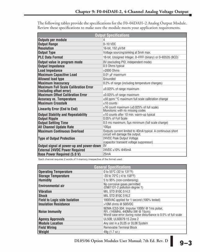
DL05/06 Option Modules User Manual; 7th Ed. Rev. D 9–3
Chapter 9: F0-04DAH-2, 4-Channel Analog Voltage Output
The following tables provide the specifications for the F0–04DAH–2 Analog Output Module. Review these specifications to make sure the module meets your application requirements.
Output SpecificationsOutputs per module 4Output Range 0–10 VDCResolution 16-bit, 152 µV/bitOutput Type Voltage sourcing/sinking at 5mA max.PLC Data Format 16-bit, Unsigned Integer, 0–FFFF (binary) or 0–65535 (BCD)*
Output value in program mode 0V (excluding PID, independent mode)Output Impedance 0.5 Ohms typicalLoad Impedance >2000 OhmsMaximum Capacitive Load 0.01 µF maximumAllowed load type GroundedMaximum Inaccuracy 0.2% of range (including temperature changes)Maximum Full Scale Calibration Error (including offset error) ±0.025% of range maximum
Maximum Offset Calibration Error ±0.025% of range maximumAccuracy vs. Temperature ±50 ppm/ °C maximum full scale calibration change Maximum Crosstalk ±10 counts
Linearity Error (End to End) ±16 count maximum (±0.025% of full scale) Monotonic with no missing codes
Output Stability and Repeatability ±10 counts after 10 min. warm-up typicalOutput Ripple 0.05% of Full ScaleOutput Settling Time 0.5 ms maximum, 5µs minimum (full scale change)All Channel Update Rate 100µsMaximum Continuous Overload Outputs current limited to 40mA typical. A continuous short
circuit will damage the output.Type of Output Protection 24VDC Peak Output Voltage
(capacitor transient voltage suppressor)Output signal at power-up and power-down 0VExternal 24VDC Power Required 24VDC ±10% @45mABase Power Required (5.0 V) 25mA
General SpecificationsOperating Temperature 0 to 55°C (32 to 131°F)Storage Temperature -20 to 70°C (-4 to 158°F)Humidity 5 to 95% (non-condensing)
Environmental air No corrosive gases permitted (EN61131-2 pollution degree 1)
Vibration MIL STD 810C 514.2Shock MIL STD 810C 516.2Field to Logic side Isolation 1800VAC applied for 1 second (100% tested)Insulation Resistance >10M ohms @ 500VDC
Noise ImmunityNEMA ICS3-304; Impulse 1000V @ 1ms pulse; RFI, (145MHz, 440Mhz 5W @ 15cm); Worst case error during noise disturbance is 0.5% of full scale
Agency Approvals UL508; UL60079-15 Zone 2Module Location Any slot in a DL05 or DL06 SystemField Wiring Removable Terminal BlockWeight 49g (1.7 oz.)
*Each channel requires 2 words of V-memory irrespective of the format used.

DL05/06 Option Modules User Manual; 7th Ed. Rev. D9–4
Chapter 9: F0-04DAH-2, 4-Channel Analog Voltage Output
Connecting and Disconnecting the Field WiringWARNING: Before removing the analog module or the terminal block on the face of the module, disconnect power to the PLC and all field devices. Failure to disconnect power can result in damage to the PLC and/or field devices.
Wiring GuidelinesYour company may have guidelines for wiring and cable installation. If so, you should check those before you begin the installation. Here are some general things to consider:
• Use the shortest wiring route whenever possible.
• Use shielded wiring and ground the shield at the transmitter source. Do not ground the shield at both the module and the source.
• Do not run the signal wiring next to large motors, high current switches, or transformers. This may cause noise problems.
• Route the wiring through an approved cable housing to minimize the risk of accidental damage. Check local and national codes to choose the correct method for your application.
The F0–04DAH–2 does not supply power to field devices. You will need to power transmitters separately from the PLC.
To remove the terminal block, disconnect power to the PLC and the field devices. Pull the terminal block firmly until the connector separates from the module.
You can remove the analog module from the PLC by folding out the retaining tabs at the top and bottom of the module. As the retaining tabs pivot upward and outward, the module’s connector is lifted out of the PLC socket. Once the connector is free, you can lift the module out of its slot.
Terminal Block SpecificationsNumber of Positions 13Re-Order Number D0-ACC-4Pitch 0.2 inch (5.08 mm)
Wire Range 28–16 AWG Solid or Stranded Conductor; Wire strip length 5/16” (7–8 mm)
Screwdriver Size (Slotted) 0.4T x 2.5W mm (part number DN-SS1)Screw Size M2.5 sizeScrew Torque 4.5 inch-pounds (0.52 N·m)

DL05/06 Option Modules User Manual; 7th Ed. Rev. D 9–5
Chapter 9: F0-04DAH-2, 4-Channel Analog Voltage Output
Wiring DiagramUse the following diagram to connect the field wiring. If necessary, the F0–04DAH–2 terminal block can be removed to make removal of the module possible without disturbing field wiring.
COM
ANALOG
0–10VDC
F0-04DAH-2
OUT
CH1
CH2
CH3
CH4
COM
COM
COM
+24V
0V
24VDCPower Supply
0VDC
+24VDC
SHIELD CONNECTED TO SIGNALSOURCE COMMON (1 OF 4 SHOWN)
CH1 DAC
CH2 DAC
CH3 DAC
CH4 DAC
isolated analog circuit common
Internal Module CircuitryTypical User Wiring
ISOLATED ANALOGCIRCUIT POWER
voltagesink / source
voltagesink / source
voltagesink / source
voltagesink / source
Voltage OutputCh. 1
Voltage OutputCh. 3
Voltage OutputCh. 4
Voltage OutputCh. 2
COM
CH1
CH3
CH2
CH4
COM
COM
COM
NOTE: To ensure that readings on unused channels are zero, installa jumper between the CHx and COM terminals on all unused channels.

DL05/06 Option Modules User Manual; 7th Ed. Rev. D9–6
Chapter 9: F0-04DAH-2, 4-Channel Analog Voltage Output
Module OperationChannel Scanning Sequence
The DL05 and DL06 will read all four channels of output data during each scan. Each CPU supports special V-memory locations that are used to manage the data transfer. This is discussed in more detail beginning in the section on “Special V-memory Locations”.
Read the data
Store data
Read Inputs
Execute Application Program
Scan
Write to Outputs
Scan N
Scan N+1
Scan N+2
Scan N+3
Scan N+4
DL05/DL06 PLC
Ch 1, 2, 3, 4
Ch 1, 2, 3, 4
Ch 1, 2, 3, 4
Ch 1, 2, 3, 4
Ch 1, 2, 3, 4
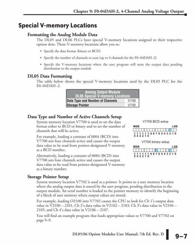
DL05/06 Option Modules User Manual; 7th Ed. Rev. D 9–7
Chapter 9: F0-04DAH-2, 4-Channel Analog Voltage Output
Special V-memory LocationsFormatting the Analog Module Data
The DL05 and DL06 PLCs have special V-memory locations assigned to their respective option slots. These V-memory locations allow you to:
• Specify the data format (binary or BCD)
• Specify the number of channels to scan (up to 4 channels for the F0–04DAH–2)
• Specify the V-memory locations where the user program will store the output data pending distribution to the output module
DL05 Data FormattingThe table below shows the special V-memory locations used by the DL05 PLC for the F0–04DAH–2.
Data Type and Number of Active Channels SetupSystem memory location V7700 is used to set the data format either to BCD or binary and to set the number of channels that will be active.
For example, loading a constant of 0004 (BCD) into V7700 sets four channels active and causes the output data value to be read from pointer-designated V-memory as a BCD number.
Alternatively, loading a constant of 0084 (BCD) into V7700 sets four channels active and causes the output data value to be read from pointer-designated V-memory as a binary number.
Storage Pointer SetupSystem memory location V7702 is used as a pointer. It points to a user memory location where the analog output data is stored by the user program, pending distribution to the output module. An octal number is loaded to the pointer memory to identify the beginning of a block of user memory where output values are stored.
For example, loading O2100 into V7702 causes the CPU to look for Ch 1’s output data value in V2100 – 2101, Ch 2’s data value in V2102 – 2103, Ch 3’s data value in V2104 – 2105, and Ch 4’s data value in V2106 – 2107.
You will find an example program that loads appropriate values to V7700 and V7702 on page 9–9.
Analog Output Module DL05 Special V-memory Locations
Data Type and Number of Channels V7700Storage Pointer V7702
MSB LSB
0115
10
11
12
13
14
789 6 5 4 3 2
MSB LSB
0115
10
11
12
13
14
789 6 5 4 3 2
V7700 BCD setup
V7700 binary setup

DL05/06 Option Modules User Manual; 7th Ed. Rev. D9–8
Chapter 9: F0-04DAH-2, 4-Channel Analog Voltage Output
DL06 Data FormattingSpecial V-memory locations are assigned to the four option slots of the DL06 PLC. The table below shows these V-memory locations which can be used to setup the F0–04DAH–2.
Data Type and Number of Active Channels SetupSystem memory locations V700, 710, 720, and 730 are used to set the data format either to BCD or binary and to set the number of channels that will be active.
For example, loading a constant of 0004 (BCD) into V700 sets four channels active and causes the output data value to be read from pointer-designated V-memory as a BCD number.
Alternatively, loading a constant of 0084 (BCD) into V700 sets four channels active and causes the output data value to be read from pointer-designated V-memory as a binary number.
Storage Pointer SetupSystem memory locations V702, 712, 722, and 732 are used as pointers. They point to user memory locations where the analog output data is stored by the user program, pending distribution to the output module. An octal number is loaded to the pointer memory to identify the beginning of a block of user memory where output values are stored.
For example, loading O2100 into V702 causes the CPU to look for Ch 1’s output data value in V2100 – 2101, Ch 2’s data value in V2102 – 2103, Ch 3’s data value in V2104 – 2105, and Ch 4’s data value in V2106 – 2107.
You will find an example program that loads appropriate values to V7700 and V7702 on page 9–10.
Analog Output Module DL06 Special V-memory Locations
Slot No. 1 2 3 4Data Type and Number of Channels V700 V710 V720 V730Output Pointer V702 V712 V722 V732
MSB LSB
0115
10
11
12
13
14
789 6 5 4 3 2
MSB LSB
0115
10
11
12
13
14
789 6 5 4 3 2
V700 BCD setup
V700 binary setup
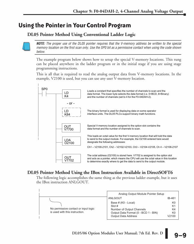
DL05/06 Option Modules User Manual; 7th Ed. Rev. D 9–9
Chapter 9: F0-04DAH-2, 4-Channel Analog Voltage Output
Using the Pointer in Your Control ProgramDL05 Pointer Method Using Conventional Ladder Logic
NOTE: The proper use of the DL05 pointer requires that the V-memory address be written to the special memory location on the first scan only. Use the SP0 bit as a permissive contact when using the code shown below.
The example program below shows how to setup the special V-memory locations. This rung can be placed anywhere in the ladder program or in the initial stage if you are using stage programming instructions.
This is all that is required to read the analog output data from V-memory locations. In the example, V2100 is used, but you can use any user V-memory location.
DL05 Pointer Method Using the IBox Instruction Available in DirectSOFT6The following logic accomplishes the same thing as the previous ladder example, but it uses the IBox instruction ANLGOUT.
SP0LD
LDAO2100
OUTV7702
Ch1 – V2100-2101, Ch2 – V2102-V2103, Ch3 – V2104-V2105, Ch 4 – V2106-2107
OUTV7700
Loads a constant that specifies the number of channels to scan and the data format. The lower byte selects the data format (i.e. 0=BCD, 8=Binary)and the number of channels (set to 4 for the F0-04DAH-2).
- or -
K4
K84LD The binary format is used for displaying data on some operator
interface units. The DL05 PLCs support binary math functions.
Special V-memory location assigned to the option slot contains thedata format and the number of channels to scan.
This loads an octal value for the first V-memory location that will hold the datato send to the output module. For example, the O2100 entered here woulddesignate the following addresses:
The octal address (O2100) is stored here. V7702 is assigned to the option slot and acts as a pointer, which means the CPU will use the octal value in this location to determine exaclty where to get the data to send to the output module.
Analog Output Module Pointer SetupANLGOUT IB-461
Base # (K0 - Local)Slot #Number of Output ChannelsOutput Data Format (0 - BCD 1 - BIN)Output Data Address
K0K1K4K0
V2100
No permissive contact or input logicis used with this instruction.

DL05/06 Option Modules User Manual; 7th Ed. Rev. D9–10
Chapter 9: F0-04DAH-2, 4-Channel Analog Voltage Output
DL06 Pointer Method Using Conventional Ladder Logic
NOTE: The proper use of the DL06 pointer requires that the V-memory address be written to the special memory location on the first scan only. Use the SP0 bit as a permissive contact when using the code shown below.
Use the special V-memory table below as a guide to setup the storage pointer in the following example for the DL06. Slot 1 is the left most option slot.
The F0–04DAH–2 can be installed in any available DL06 option slot. The ladder diagram below shows how to setup these locations with the module installed in slot 1 of the DL06. Use the above table to determine the pointer values if locating the module in any of the other slot locations. Place this rung anywhere in the ladder program or in the initial stage if you are using stage programming instructions.
This logic is all that is required to write the analog output data from V-memory locations. In the example, V2100 is used, but you can use any user V-memory location.
Analog Output Module DL06 Special V-memory Locations
Slot No. 1 2 3 4No. of Channels V700 V710 V720 V730Output Pointer V702 V712 V722 V732
SP0LD
LDAO2100
OUTV702
OUTV700
K4
K84LD
Ch1 – V2100-2101, Ch2 – V2102-V2103, Ch3 – V2104-V2105, Ch 4 – V2106-2107.
Loads a constant that specifies the number of channels to scan and the data format. The lower byte selects the data format (i.e. 0=BCD, 8=Binary)and the number of channels (set to 4 for the F0-04DAH-2).
The binary format is used for displaying data on some operatorinterface units and the DL06 display. The DL06 PLCs support binary math functions.
Special V-memory location assigned to the first option slot contains thedata format and the number of channels to scan.
This loads an octal value for the first V-memory location that will hold the datato send to the output module. For example, the O2100 entered here woulddesignate the following addresses:
The octal address (O2100) is stored here. V702 is assigned to the first option slot and acts as a pointer, which means the CPU will use the octal value in this location to determine exaclty where to get the data to send to the output module.
- or -
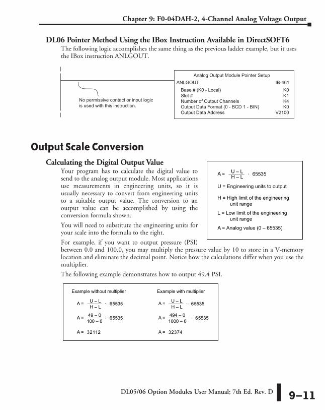
DL05/06 Option Modules User Manual; 7th Ed. Rev. D 9–11
Chapter 9: F0-04DAH-2, 4-Channel Analog Voltage Output
DL06 Pointer Method Using the IBox Instruction Available in DirectSOFT6The following logic accomplishes the same thing as the previous ladder example, but it uses the IBox instruction ANLGOUT.
Output Scale ConversionCalculating the Digital Output Value
Your program has to calculate the digital value to send to the analog output module. Most applications use measurements in engineering units, so it is usually necessary to convert from engineering units to a suitable output value. The conversion to an output value can be accomplished by using the conversion formula shown.
You will need to substitute the engineering units for your scale into the formula to the right.
For example, if you want to output pressure (PSI) between 0.0 and 100.0, you may multiply the pressure value by 10 to store in a V-memory location and eliminate the decimal point. Notice how the calculations differ when you use the multiplier.
The following example demonstrates how to output 49.4 PSI.
Analog Output Module Pointer SetupANLGOUT IB-461
Base # (K0 - Local)Slot #Number of Output ChannelsOutput Data Format (0 - BCD 1 - BIN)Output Data Address
K0K1K4K0
V2100
No permissive contact or input logicis used with this instruction.
Example without multiplier Example with multiplier
A = U – L 65535H – L
A = 32112
A = 49 – 0 65535100 – 0
A = U – L 65535H – L
A = 32374
A = 494 – 0 655351000 – 0
H = High limit of the engineeringunit range
L = Low limit of the engineering unit range
A = Analog value (0 – 65535)
A = U – L 65535H – L
U = Engineering units to output
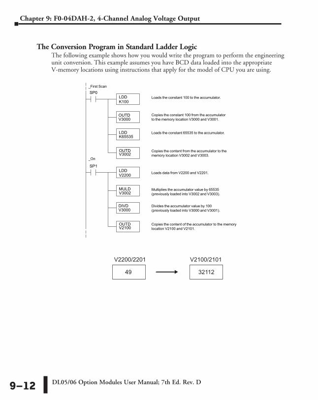
DL05/06 Option Modules User Manual; 7th Ed. Rev. D9–12
Chapter 9: F0-04DAH-2, 4-Channel Analog Voltage Output
The Conversion Program in Standard Ladder LogicThe following example shows how you would write the program to perform the engineering unit conversion. This example assumes you have BCD data loaded into the appropriate V-memory locations using instructions that apply for the model of CPU you are using.
SP0LDD
LDDK65535
OUTDV3002
OUTDV3000
K100
SP1LDD
OUTDV2100
V2200
Loads the constant 100 to the accumulator.
Copies the constant 100 from the accumulatorto the memory location V3000 and V3001.
Loads the constant 65535 to the accumulator.
Copies the content from the accumulator to the memory location V3002 and V3003.
_First Scan
_On
Loads data from V2200 and V2201.
Copies the content of the accumulator to the memory location V2100 and V2101.
DIVDV3000
Divides the accumulator value by 100 (previously loaded into V3000 and V3001).
MULDV3002
Multiplies the accumulator value by 65535 (previously loaded into V3002 and V3003).
49
V2200/2201
32112
V2100/2101

DL05/06 Option Modules User Manual; 7th Ed. Rev. D 9–13
Chapter 9: F0-04DAH-2, 4-Channel Analog Voltage Output
Analog and Digital Value ConversionsSometimes it is useful to convert between the signal levels and the digital values. This is especially helpful during machine startup or troubleshooting. The following table provides formulas to make this conversion easier.
The formulas in the table show the relationship between A, the analog value, and D, the digital value.
For example, if you need a 6VDC signal to achieve the desired result, you can use the formula to determine the digital value that should be used.
D =
D =
D = 39321
6553510 A
6553510 6V
Range If you know the digital value If you know the analog signal level
0 to 10VDC A = . D65535
10 D = . A6553510

DL05/06 Option Modules User Manual; 7th Ed. Rev. D9–14
Chapter 9: F0-04DAH-2, 4-Channel Analog Voltage Output
Module ResolutionAnalog Data Bits
Two 16-bit words are reserved for the analog data whether you are using BCD or binary data formatting. The 16 bits in the low word represent the analog data in binary format.
Resolution DetailsSince the module has 16-bit resolution, the analog signal is converted into 65536 counts ranging from 0–65535 (216). A 0VDC signal would be 0 and a 10VDC signal would be 65535. This is equivalent to a binary value of 0000 0000 0000 0000 to 1111 1111 1111 1111, or 000 to FFFF hexadecimal.
Each count can also be expressed in terms of the signal level by using the following equation:
The following table shows the smallest detectable signal change that will result in one LSB change in the data value for each increment of the signal change.
VDC Range Signal Span (H – L) Divide By Smallest Detectable
Change0 to 10 VDC 10VDC 65535 153µV
0 – 10V
0 65535
0V
10VResolution =
H – L
65535
H = high limit of the signal range
L = low limit of the signal range
MSB LSB
013 2
MSB LSB
013 2
BCD Example
V2000V2001
MSB LSB
0115
10
11
12
13
14
789 6 5 4 3 2
= data bits
MSB LSB
15
10
11
12
13
14
789 6 5 4 013 2
V2000V2001
Binary Example
013 2013 2013 2

F0-08DAH-2, 8-CHAnnel AnAlog VoltAge output
ChapterChapterChapter
41010In This Chapter...
Module Specifications .............................................................................................10–2
Connecting and Disconnecting the Field Wiring ...................................................10–4
Wiring Diagram .......................................................................................................10–5
Module Operation ...................................................................................................10–6
Special V-memory Locations ...................................................................................10–7
Using the Pointer in Your Control Program ...........................................................10–9
Output Scale Conversion .......................................................................................10–11
Module Resolution .................................................................................................10–14
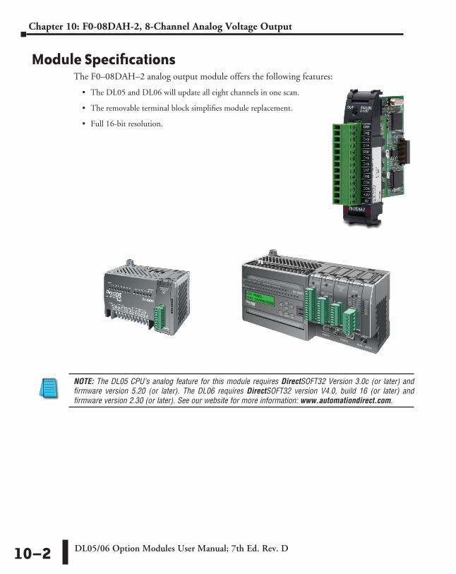
DL05/06 Option Modules User Manual; 7th Ed. Rev. D10–2
Chapter 10: F0-08DAH-2, 8-Channel Analog Voltage Output
Module SpecificationsThe F0–08DAH–2 analog output module offers the following features:
• The DL05 and DL06 will update all eight channels in one scan.
• The removable terminal block simplifies module replacement.
• Full 16-bit resolution.
NOTE: The DL05 CPU’s analog feature for this module requires DirectSOFT32 Version 3.0c (or later) and firmware version 5.20 (or later). The DL06 requires DirectSOFT32 version V4.0, build 16 (or later) and firmware version 2.30 (or later). See our website for more information: www.automationdirect.com.

DL05/06 Option Modules User Manual; 7th Ed. Rev. D 10–3
Chapter 10: F0-08DAH-2, 8-Channel Analog Voltage Output
The following tables provide the specifications for the F0–08DAH –2 Analog Output Module. Review these specifications to make sure the module meets your application requirements.
Output SpecificationsOutputs per module 8Output Range 0–10 VDCResolution 16-bit, 152 µV/bitOutput Type Voltage sourcing/sinking at 5mA max.PLC Data Format 16-bit, Unsigned Integer, 0–FFFF (binary) or 0–65535 (BCD)*
Output value in program mode 0V (excluding PID, independent mode)Output Impedance 0.5 Ohms typicalLoad Impedance >2000 OhmsMaximum Capacitive Load 0.01 µF maximumAllowed load type GroundedMaximum Inaccuracy 0.27% of range (including temperature changes)Maximum Full Scale Calibration Error (including offset error) ±0.025% of range maximum
Maximum Offset Calibration Error ±0.025% of range maximumAccuracy vs. Temperature ±50 ppm/ °C maximum full scale calibration change Maximum Crosstalk at DC, 50 Hz and 60 Hz. 10 counts
Linearity Error (End to End) ±16 count maximum (±0.025% of full scale) Monotonic with no missing codes
Output Stability and Repeatability ±10 counts after 10 min. warm-up typicalOutput Ripple 0.05% of Full ScaleOutput Settling Time 0.5 ms maximum, 5µs minimum (full scale change)All Channel Update Rate 100µsMaximum Continuous Overload Outputs current limited to 40mA typical. A continuous short
circuit will damage the output.Type of Output Protection 24VDC Peak Output Voltage
(capacitor transient voltage suppressor)Output signal at power-up and power-down 0VExternal 24VDC Power Required 24VDC ±10% @ 75mABase Power Required (5.0 V) 25mA
General SpecificationsOperating Temperature 0 to 55°C (32 to 131°F)Storage Temperature -20 to 70°C (-4 to 158°F)Humidity 5 to 95% (non-condensing)
Environmental air No corrosive gases permitted (EN61131-2 pollution degree 1)
Vibration MIL STD 810C 514.2Shock MIL STD 810C 516.2Field to Logic side Isolation 1800VAC applied for 1 second (100% tested)Insulation Resistance >10M ohms @ 500VDC
Noise ImmunityNEMA ICS3-304; Impulse 1000V @ 1ms pulse; RFI, (145MHz, 440MHz 5W @ 15cm); Worst case error during noise disturbance is 0.5% of full scale
Agency Approvals UL508; UL60079-15 Zone 2Module Location Any slot in a DL05 or DL06 SystemField Wiring Removable Terminal BlockWeight 49g (1.7 oz.)
*Each channel requires 2 words of V-memory irrespective of the format used.
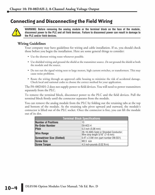
DL05/06 Option Modules User Manual; 7th Ed. Rev. D10–4
Chapter 10: F0-08DAH-2, 8-Channel Analog Voltage Output
Connecting and Disconnecting the Field WiringWARNING: Before removing the analog module or the terminal block on the face of the module, disconnect power to the PLC and all field devices. Failure to disconnect power can result in damage to the PLC and/or field devices.
Wiring GuidelinesYour company may have guidelines for wiring and cable installation. If so, you should check those before you begin the installation. Here are some general things to consider:
• Use the shortest wiring route whenever possible.
• Use shielded wiring and ground the shield at the transmitter source. Do not ground the shield at both the module and the source.
• Do not run the signal wiring next to large motors, high current switches, or transformers. This may cause noise problems.
• Route the wiring through an approved cable housing to minimize the risk of accidental damage. Check local and national codes to choose the correct method for your application.
The F0–08DAH–2 does not supply power to field devices. You will need to power transmitters separately from the PLC.
To remove the terminal block, disconnect power to the PLC and the field devices. Pull the terminal block firmly until the connector separates from the module.
You can remove the analog module from the PLC by folding out the retaining tabs at the top and bottom of the module. As the retaining tabs pivot upward and outward, the module’s connector is lifted out of the PLC socket. Once the connector is free, you can lift the module out of its slot.
Terminal Block SpecificationsNumber of Positions 13Re-Order Number D0-ACC-4Pitch 0.2 inch (5.08 mm)
Wire Range 28–16 AWG Solid or Stranded Conductor; Wire strip length 5/16” (7–8 mm)
Screwdriver Size (Slotted) 0.4T x 2.5W mm (part number DN-SS1)Screw Size M2.5 sizeScrew Torque 4.5 inch-pounds (0.52 N·m)

DL05/06 Option Modules User Manual; 7th Ed. Rev. D 10–5
Chapter 10: F0-08DAH-2, 8-Channel Analog Voltage Output
Wiring DiagramUse the following diagram to connect the field wiring. If necessary, the F0–08DAH–2 terminal block can be removed to make removal of the module possible without disturbing field wiring.
ANALOG
0–10VDC
F0-08DAH-2
OUT
CH1
CH2
CH3
CH4
COM
CH5
CH6
CH7
CH8
COM
COM
+24V
0V
24VDCPower Supply
0VDC
+24VDC
COM
COM
SHIELD CONNECTED TO SIGNALSOURCE COMMON (1 OF 8 SHOWN)
CH1 DAC
CH2 DAC
CH3 DAC
CH4 DAC
CH5 DAC
CH6 DAC
CH7 DAC
CH8 DAC
isolated analog circuit common
Internal Module CircuitryTypical User Wiring
ISOLATED ANALOGCIRCUIT POWER
voltagesink / source
voltagesink / source
voltagesink / source
voltagesink / source
voltagesink / source
voltagesink / source
voltagesink / source
voltagesink / source
Voltage OutputCh. 1
Voltage OutputCh. 8
Voltage OutputCh. 3
Voltage OutputCh. 4
Voltage OutputCh. 5
Voltage OutputCh. 6
Voltage OutputCh. 7
Voltage OutputCh. 2
COM
CH5
CH1
CH8
CH3
CH2
CH4
CH7
CH6
NOTE: To ensure that readings on unused channels are zero, installa jumper between the CHx and COM terminals on all unused channels.
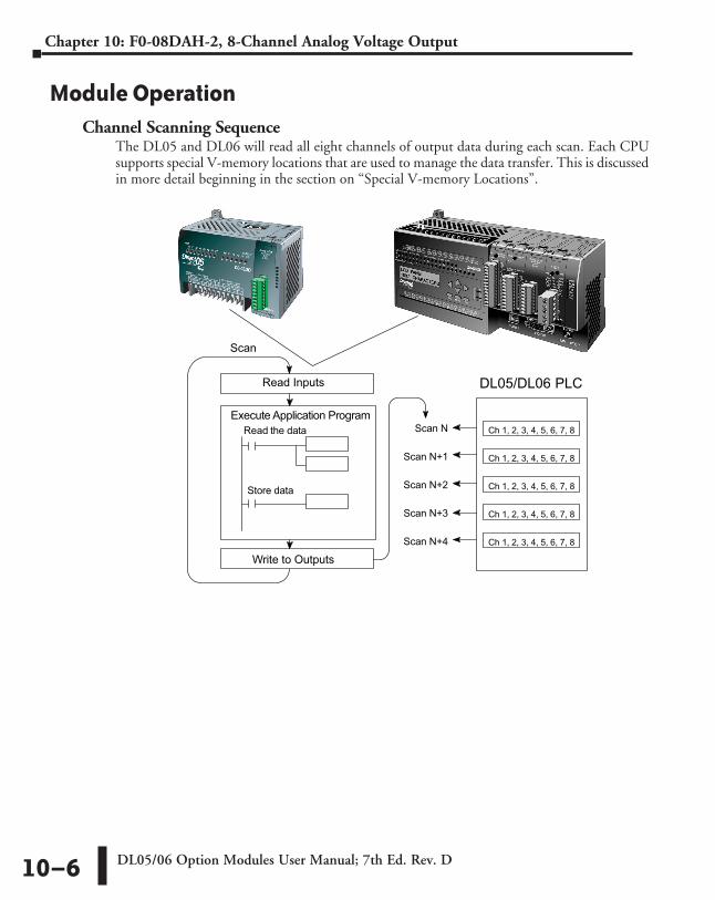
DL05/06 Option Modules User Manual; 7th Ed. Rev. D10–6
Chapter 10: F0-08DAH-2, 8-Channel Analog Voltage Output
Module OperationChannel Scanning Sequence
The DL05 and DL06 will read all eight channels of output data during each scan. Each CPU supports special V-memory locations that are used to manage the data transfer. This is discussed in more detail beginning in the section on “Special V-memory Locations”.
Read the data
Store data
Read Inputs
Execute Application Program
Scan
Write to Outputs
Scan N
Scan N+1
Scan N+2
Scan N+3
Scan N+4
DL05/DL06 PLC
Ch 1, 2, 3, 4, 5, 6, 7, 8
Ch 1, 2, 3, 4, 5, 6, 7, 8
Ch 1, 2, 3, 4, 5, 6, 7, 8
Ch 1, 2, 3, 4, 5, 6, 7, 8
Ch 1, 2, 3, 4, 5, 6, 7, 8

DL05/06 Option Modules User Manual; 7th Ed. Rev. D 10–7
Chapter 10: F0-08DAH-2, 8-Channel Analog Voltage Output
Special V-memory LocationsFormatting the Analog Module Data
The DL05 and DL06 PLCs have special V-memory locations assigned to their respective option slots. These V-memory locations allow you to:
• Specify the data format (binary or BCD)
• Specify the number of channels to scan (up to 8 channels for the F0–08DAH–2)
• Specify the V-memory locations where the user program will store the output data pending distribution to the output module
DL05 Data FormattingThe table below shows the special V-memory locations used by the DL05 PLC for the F0–08DAH–2.
Data Type and Number of Active Channels SetupSystem memory location V7700 is used to set the data format either to BCD or binary and to set the number of channels that will be active.
For example, loading a constant of 0008 (BCD) into V7700 sets eight channels active and causes the output data value to be read from pointer-designated V-memory as a BCD number.
Alternatively, loading a constant of 0088 (BCD) into V7700 sets eight channels active and causes the output data value to be read from pointer-designated V-memory as a binary number.
Storage Pointer SetupSystem memory location V7702 is used as a pointer. It points to a user memory location where the analog output data is stored by the user program, pending distribution to the output module. An octal number is loaded to the pointer memory to identify the beginning of a block of user memory where output values are stored.
For example, loading O2100 into V7702 causes the CPU to look for Ch 1’s output data value in V2100 – 2101, Ch 2’s data value in V2102 – 2103, Ch 3’s data value in V2104 – 2105, Ch 4’s data value in V2106 – 2107, Ch 5’s data value in V2110 – 2111, Ch 6’s data value in V2112 – 2113, Ch 7’s data value in V2114 – 2115, and Ch 8’s data value in V2116 – 2117.
You will find an example program that loads appropriate values to V7700 and V7702 on page 10–9.
Analog Output Module DL05 Special V-memory Locations
Data Type and Number of Channels V7700Storage Pointer V7702
MSB LSB
0115
10
11
12
13
14
789 6 5 4 3 2
MSB LSB
0115
10
11
12
13
14
789 6 5 4 3 2
V7700 BCD setup
V7700 binary setup

DL05/06 Option Modules User Manual; 7th Ed. Rev. D10–8
Chapter 10: F0-08DAH-2, 8-Channel Analog Voltage Output
DL06 Data FormattingSpecial V-memory locations are assigned to the four option slots of the DL06 PLC. The table below shows these V-memory locations which can be used to setup the F0–08DAH–2.
Data Type and Number of Active Channels SetupSystem memory locations V700, 710, 720, and 730 are used to set the data format either to BCD or binary and to set the number of channels that will be active.
For example, loading a constant of 0008 (BCD) into V700 sets eight channels active and causes the output data value to be read from pointer-designated V-memory as a BCD number.
Alternatively, loading a constant of 0088 (BCD) into V700 sets eight channels active and causes the output data value to be read from pointer-designated V-memory as a binary number.
Storage Pointer SetupV-memory locations 702, 712, 722 and 732 are special locations used as storage pointers. A V-memory address is loaded into this location as an octal number identifying the first user V-memory location for the analog output data. This V-memory location is user selectable. For example, loading O2100 causes the pointer to write Ch 1’s data value to V2100 – 2101, Ch 2’s data value to V2102 – 2103, Ch 3’s data value to V2104 – 2105, Ch 4’s data value to V2106 – 2107, Ch 5’s data value to V2110 – 2111, Ch 6’s data value to V2112 – 2113, Ch 7’s data value to V2114 – 2115, and Ch 8’s data value to V2116 – 2117.
You will find an example program that loads appropriate values to V700 and V702 beginning on page 10–10.
Analog Output Module DL06 Special V-memory Locations
Slot No. 1 2 3 4Data Type and Number of Channels V700 V710 V720 V730Output Pointer V702 V712 V722 V732
MSB LSB
0115
10
11
12
13
14
789 6 5 4 3 2
MSB LSB
0115
10
11
12
13
14
789 6 5 4 3 2
V7700 BCD setup
V7700 binary setup
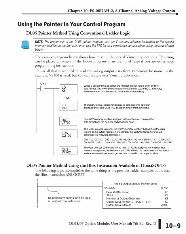
DL05/06 Option Modules User Manual; 7th Ed. Rev. D 10–9
Chapter 10: F0-08DAH-2, 8-Channel Analog Voltage Output
Using the Pointer in Your Control ProgramDL05 Pointer Method Using Conventional Ladder Logic
NOTE: The proper use of the DL05 pointer requires that the V-memory address be written to the special memory location on the first scan only. Use the SP0 bit as a permissive contact when using the code shown below.
The example program below shows how to setup the special V-memory locations. This rung can be placed anywhere in the ladder program or in the initial stage if you are using stage programming instructions.
This is all that is required to read the analog output data from V-memory locations. In the example, V2100 is used, but you can use any user V-memory location.
DL05 Pointer Method Using the IBox Instruction Available in DirectSOFT6The following logic accomplishes the same thing as the previous ladder example, but it uses the IBox instruction ANLGOUT.
SP0LD
LDAO2100
OUTV7702
Ch1 – V2100-2101, Ch2 – V2102-V2103, Ch3 – V2104-V2105, Ch 4 – V2106-2107Ch 5 – V2110-2111, Ch 6 – V2112-V2113, Ch 7 – V2114-V2115, Ch 8 – V2116-V2117.
OUTV7700
Loads a constant that specifies the number of channels to scan and the data format. The lower byte selects the data format (i.e. 0=BCD, 8=Binary)and the number of channels (up to 8 for the F0-08DAH-2).
- or -
K8
K88LD The binary format is used for displaying data on some operator
interface units. The DL05 PLCs support binary math functions.
Special V-memory location assigned to the option slot contains thedata format and the number of channels to scan.
This loads an octal value for the first V-memory location that will hold the datato send to the output module. For example, the O2100 entered here woulddesignate the following addresses:
The octal address (O2100) is stored here. V7702 is assigned to the option slot and acts as a pointer, which means the CPU will use the octal value in this location to determine exaclty where to get the data to send to the output module.
Analog Output Module Pointer SetupANLGOUT IB-461
Base # (K0 - Local)Slot #Number of Output ChannelsOutput Data Format (0 - BCD 1 - BIN)Output Data Address
K0K1K8K0
V2100
No permissive contact or input logicis used with this instruction.
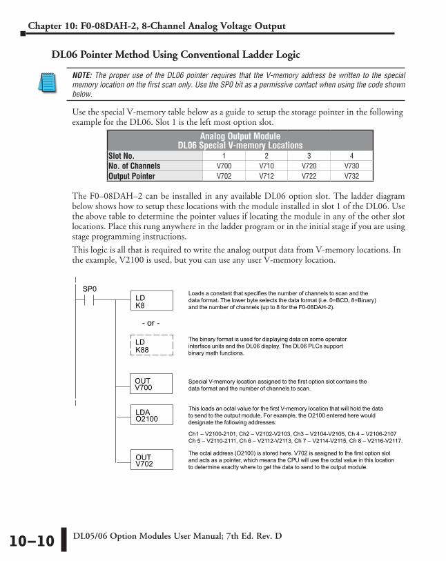
DL05/06 Option Modules User Manual; 7th Ed. Rev. D10–10
Chapter 10: F0-08DAH-2, 8-Channel Analog Voltage Output
DL06 Pointer Method Using Conventional Ladder Logic
NOTE: The proper use of the DL06 pointer requires that the V-memory address be written to the special memory location on the first scan only. Use the SP0 bit as a permissive contact when using the code shown below.
Use the special V-memory table below as a guide to setup the storage pointer in the following example for the DL06. Slot 1 is the left most option slot.
The F0–08DAH–2 can be installed in any available DL06 option slot. The ladder diagram below shows how to setup these locations with the module installed in slot 1 of the DL06. Use the above table to determine the pointer values if locating the module in any of the other slot locations. Place this rung anywhere in the ladder program or in the initial stage if you are using stage programming instructions.
This logic is all that is required to write the analog output data from V-memory locations. In the example, V2100 is used, but you can use any user V-memory location.
Analog Output Module DL06 Special V-memory Locations
Slot No. 1 2 3 4No. of Channels V700 V710 V720 V730Output Pointer V702 V712 V722 V732
SP0LD
LDAO2100
OUTV702
OUTV700
K8
K88LD
Ch1 – V2100-2101, Ch2 – V2102-V2103, Ch3 – V2104-V2105, Ch 4 – V2106-2107Ch 5 – V2110-2111, Ch 6 – V2112-V2113, Ch 7 – V2114-V2115, Ch 8 – V2116-V2117.
Loads a constant that specifies the number of channels to scan and the data format. The lower byte selects the data format (i.e. 0=BCD, 8=Binary)and the number of channels (up to 8 for the F0-08DAH-2).
The binary format is used for displaying data on some operatorinterface units and the DL06 display. The DL06 PLCs support binary math functions.
Special V-memory location assigned to the first option slot contains thedata format and the number of channels to scan.
This loads an octal value for the first V-memory location that will hold the datato send to the output module. For example, the O2100 entered here woulddesignate the following addresses:
The octal address (O2100) is stored here. V702 is assigned to the first option slot and acts as a pointer, which means the CPU will use the octal value in this location to determine exaclty where to get the data to send to the output module.
- or -
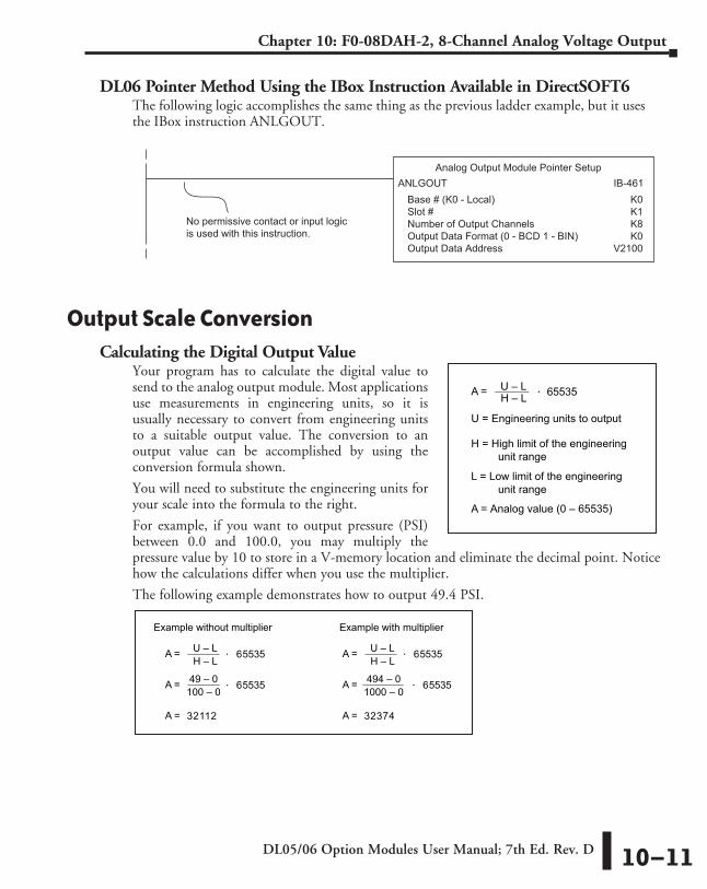
DL05/06 Option Modules User Manual; 7th Ed. Rev. D 10–11
Chapter 10: F0-08DAH-2, 8-Channel Analog Voltage Output
DL06 Pointer Method Using the IBox Instruction Available in DirectSOFT6The following logic accomplishes the same thing as the previous ladder example, but it uses the IBox instruction ANLGOUT.
Output Scale ConversionCalculating the Digital Output Value
Your program has to calculate the digital value to send to the analog output module. Most applications use measurements in engineering units, so it is usually necessary to convert from engineering units to a suitable output value. The conversion to an output value can be accomplished by using the conversion formula shown.
You will need to substitute the engineering units for your scale into the formula to the right.
For example, if you want to output pressure (PSI) between 0.0 and 100.0, you may multiply the pressure value by 10 to store in a V-memory location and eliminate the decimal point. Notice how the calculations differ when you use the multiplier.
The following example demonstrates how to output 49.4 PSI.
Analog Output Module Pointer SetupANLGOUT IB-461
Base # (K0 - Local)Slot #Number of Output ChannelsOutput Data Format (0 - BCD 1 - BIN)Output Data Address
K0K1K8K0
V2100
No permissive contact or input logicis used with this instruction.
Example without multiplier Example with multiplier
A = U – L 65535H – L
A = 32112
A = 49 – 0 65535100 – 0
A = U – L 65535H – L
A = 32374
A = 494 – 0 655351000 – 0
H = High limit of the engineeringunit range
L = Low limit of the engineering unit range
A = Analog value (0 – 65535)
A = U – L 65535H – L
U = Engineering units to output

DL05/06 Option Modules User Manual; 7th Ed. Rev. D10–12
Chapter 10: F0-08DAH-2, 8-Channel Analog Voltage Output
The Conversion Program in Standard Ladder LogicThe following example shows how you would write the program to perform the engineering unit conversion. This example assumes you have BCD data loaded into the appropriate V-memory locations using instructions that apply for the model of CPU you are using.
SP0LDD
LDDK65535
OUTDV3002
OUTDV3000
K100
SP1LDD
OUTDV2100
V2200
Loads the constant 100 to the accumulator.
Copies the constant 100 from the accumulatorto the memory location V3000 and V3001.
Loads the constant 65535 to the accumulator.
Copies the content from the accumulator to the memory location V3002 and V3003.
_First Scan
_On
Loads data from V2200 and V2201.
Copies the content of the accumulator to the memory location V2100 and V2101.
DIVDV3000
Divides the accumulator value by 100 (previously loaded into V3000 and V3001).
MULDV3002
Multiplies the accumulator value by 65535 (previously loaded into V3002 and V3003).
49
V2200/2201
32112
V2100/2101

DL05/06 Option Modules User Manual; 7th Ed. Rev. D 10–13
Chapter 10: F0-08DAH-2, 8-Channel Analog Voltage Output
Analog and Digital Value ConversionsSometimes it is useful to convert between the signal levels and the digital values. This is especially helpful during machine startup or troubleshooting. The following table provides formulas to make this conversion easier.
The formulas in the table show the relationship between A, the analog value, and D, the digital value.
For example, if you need a 6VDC signal to achieve the desired result, you can use the formula to determine the digital value that should be used.
Range If you know the digital value If you know the analog signal level
0 to 10VDC A = . D65535
10 D = . A6553510
D =
D =
D = 39321
6553510 A
6553510 6V

DL05/06 Option Modules User Manual; 7th Ed. Rev. D10–14
Chapter 10: F0-08DAH-2, 8-Channel Analog Voltage Output
Module ResolutionAnalog Data Bits
Two 16-bit words are reserved for the analog data whether you are using BCD or binary data formatting. The 16 bits in the low word represent the analog data in binary format.
Resolution DetailsSince the module has 16-bit resolution, the analog signal is converted into 65536 counts ranging from 0–65535 (216). A 0VDC signal would be 0 and a 10VDC signal would be 65535. This is equivalent to a binary value of 0000 0000 0000 0000 to 1111 1111 1111 1111, or 000 to FFFF hexadecimal.
Each count can also be expressed in terms of the signal level by using the following equation:
The following table shows the smallest detectable signal change that will result in one LSB change in the data value for each increment of the signal change.
VDC Range Signal Span (H – L) Divide By Smallest Detectable
Change0 to 10VDC 10VDC 65535 153µV
0 – 10V
0 65535
0V
10VResolution =
H – L
65535
H = high limit of the signal range
L = low limit of the signal range
MSB LSB
013 2
MSB LSB
013 2
BCD Example
V2000V2001
MSB LSB
0115
10
11
12
13
14
789 6 5 4 3 2
= data bits
MSB LSB
15
10
11
12
13
14
789 6 5 4 013 2
V2000V2001
Binary Example
013 2013 2013 2

111111F0-4AD2DA-1, 4-ChAnnel In/2-Ch. Out AnAlOg Current COmbInAtIOn
ChapterChapterChapter
In This Chapter...Module Specifications .............................................................................................11–2
Setting the Module Jumper .....................................................................................11–4
Connecting and Disconnecting the Field Wiring ...................................................11–5
Wiring Diagram .......................................................................................................11–6
Module Operation ...................................................................................................11–7
Special V-memory Locations ...................................................................................11–8
Using the Pointer in Your Control Program .........................................................11–11
Scale Conversions ..................................................................................................11–13
Special Relays .........................................................................................................11–16
Module Resolution .................................................................................................11–18
Analog Input Ladder Logic Filter ..........................................................................11–19

DL05/06 Option Modules User Manual; 7th Ed. Rev. D11–2
Chapter 11: F0-4AD2DA-1, 4-Ch. In/2-Ch. Out Analog Current Combination
Module SpecificationsThe F0-4AD2DA-1 Analog Combination module offers the following features:
• The analog input and output channels are updated in one scan.
• The removable terminal block makes it possible to remove the module without disconnecting the field wiring.
• Analog inputs can be used as process variables for the four (4) PID loops in the DL05 and the eight (8) PID loops in the DL06 CPUs.
• On-board active analog filtering and RISC-like microcontroller provide digital signal processing to maintain precise analog measurements in noisy environments.
NOTE: The DL05 CPU’s analog feature for this module requires DirectSOFT32 Version 3.0c (or later) and firmware version 3.30 (or later). The DL06 requires DirectSOFT32 version V4.0, build 16 (or later) and firmware version 1.00 (or later). See our website for more information: www.automationdirect.com.
PWR
RUN
CPU
TX1
RX1
TX2
RX2

DL05/06 Option Modules User Manual; 7th Ed. Rev. D 11–3
Chapter 11: F0-4AD2DA-1, 4-Ch. In/2-Ch. Out Analog Current Combination
The following tables provide the specifications for the F0–4AD2DA–1 Analog Combination Module. Review these specifications to make sure the module meets your application requirements.
Input SpecificationsNumber of Channels 4, single ended (one common)Input Range 0 to 20mA or 4 to 20mA (jumper selectable)Resolution 12 bit (1 in 4096) for 0–20 mA, scaled for 4–20 mAStep Response 25.0 ms (typ) to 95% of full step changeCrosstalk -80dB, 1/2 count maximum*Active Low-pass Filtering -3dB at 40Hz (-12dB per octave)Input Impedance 125 Ohm _0.1%, 1/8 W current inputAbsolute Maximum Ratings -30mA to +30mA current inputConverter type Successive approximationLinearity Error (End to End) ±2 countsInput Stability ±1 count*Full Scale Calibration Error(Offset error not included)
±10 counts maximum @ 20mA current input*
Offset Calibration Error ±5 counts maximum @ 0mA current input*
Maximum Inaccuracy ±0.4% @ 25°C (77°F)±0.85% 0 to 60°C (32 to 140°F)
Accuracy vs Temperature ±100ppm typical full scale calibration(Including maximum offset change)
Recommended Fuse (external) 0.032 A Series 217 fast-acting, current inputs*One count in the specification table is equal to one least significant bit of the analog data value (1 in 4096).
Output SpecificationsNumber of Channels 2, single ended (one common)Output Range 4 to 20mA or 0 to 20mA (jumper selectable)Output Type Current sourcingResolution 12 bit (1 in 4096) for 0 to 20mA, scaled for 4 to 20mAMaximum Loop Voltage 30VDCLoad (ohms)/Loop Power Supply 0–300/18–30 VLinearity Error (end to end) ± 2 counts (± 0.050% of full scale) maximum*Conversion Settling Time 400µS max. full scale changeFull Scale Calibration ErrorNote: Error depends on the load fromsource terminal to ground.
± 26 counts max. @ 300q load± 18 counts max. @ 250q load± 12 counts max. @ 125q load
Offset Calibration Error± 10 counts max. @ 300q load± 8 counts max @ 250q load± 6 counts max. @ 125q load
Max. Full Scale Inaccuracy(% of full scale) all errors included
300q load 0.4% @ 60°C250q load 0 3%@60°C125q load 0.2% @ 60°C
* One count in the specification tables is equal to one least significant bit of the analog data value (1 in 4096).

DL05/06 Option Modules User Manual; 7th Ed. Rev. D11–4
Chapter 11: F0-4AD2DA-1, 4-Ch. In/2-Ch. Out Analog Current Combination
Setting the Module JumperThe position of the J2 jumper determines the input and output signal level. You can choose between 0–20 mA and 4–20 mA signal levels. The module ships without the jumper connecting the pins (pins not jumpered). In this position, the input and output signal level is 4–20 mA. To select 0–20 mA signal level, install the jumper, connecting the pins.
The J2 jumper is shown in the 4–20 mA position (not installed). Install the jumper for the 0–20 mA position.
WARNING: Before removing the analog module or the terminal block on the face of the module, disconnect power to the PLC and all field devices. Failure to disconnect power can result in damage to the PLC and/or field devices.
C14
J2
General SpecificationsPLC Update Rate 4 input channels per scan, 2 output channels per scan
16-bit Data Word 12 binary data bits
Operating Temperature 0 to 60°C (32 to 140°F)
Storage Temperature -20 to 70°C (-4 to 158°F)
Relative Humidity 5 to 95% (non-condensing)
Environmental Air No corrosive gases permitted
Vibration MIL STD 810C 514.2
Shock MIL STD 810C 516.2
Noise Immunity NEMA ICS3-304
Power Budget Requirement 100mA @ 5VDC (supplied by base)
Connector Phoenix Mecano, Inc., Part No. AK1550/8-3.5 - green
Connector Wire Size 28–16 AWG
Connector Screw Torque 3.5 inch-pounds (0.4 N·m)
Connector Screwdriver Size DN-SS1 (recommended)

DL05/06 Option Modules User Manual; 7th Ed. Rev. D 11–5
Chapter 11: F0-4AD2DA-1, 4-Ch. In/2-Ch. Out Analog Current Combination
Connecting and Disconnecting the Field WiringWiring Guidelines
Your company may have guidelines for wiring and cable installation. If so, you should check those before you begin the installation. Here are some general things to consider:
• Use the shortest wiring route whenever possible.
• Use shielded wiring and ground the shield at the transmitter source. Do not ground the shield at both the module and the source.
• Do not run the signal wiring next to large motors, high current switches, or transformers. This may cause noise problems.
• Route the wiring through an approved cable housing to minimize the risk of accidental damage. Check local and national codes to choose the correct method for your application.
A separate transmitter power supply may be required, depending on the type of transmitter being used.
This module has a removable connector to make wiring and module removal easier. To remove the terminal block, disconnect power to the PLC and the field devices. Pull the terminal block firmly until the connector separates from the module.
The analog module can be removed from the PLC by folding out the retaining tabs at the top and bottom of the module. As the retaining tabs pivot upward and outward, the module’s connector is lifted out of the PLC socket. Once the connector is free, you can lift the module out of its slot.

DL05/06 Option Modules User Manual; 7th Ed. Rev. D11–6
Chapter 11: F0-4AD2DA-1, 4-Ch. In/2-Ch. Out Analog Current Combination
Wiring DiagramUse the following diagram to connect the field wiring. If necessary, the terminal block can be removed to make removal of the module possible without disturbing field wiring.
Current Loop Transmitter ImpedanceManufacturers of transmitters and transducers specify a wide variety of power sources for their products. Follow the manufacturer’s recommendations.
In some cases, manufacturers specify a minimum loop or load resistance that must be used with the transmitter. The F0-04AD2DA-1 provides 125 ohm resistance for each channel. If your transmitter requires a load resistance below 125 ohms, you do not have to make any changes. However, if your transmitter requires a load resistance higher than 125 ohms, you need to add a resistor in series with the module.
Consider the following example for a transmitter being operated from a 30VDC supply with a recommended load resistance of 750 ohms. Since the module has a 125 ohm resistor, you need to add an additional resistor.
R = Tr–Mr R = resistor to add
R = 750–125 Tr = Transmitter Requirement
R M 625 Mr = Module resistance (internal 125 ohms)
CH1
Transmitter
A to DConverter
InternalModuleWiring
Analog S
witch
See NOTE 1–
–
+
+
A n a lo g In/Out
NOTE 1: Shields should be grounded at the signalsource.
NOTE 2: Connect all external power supply commons.
4–20mA
4–In/2–Out
F0–4AD2DA–1
1
IN
2
1
2
OUT
0V
Current2–wire
1
IN
2
1
OUT
2
0V
24V
CH 1 load
maximumresistance
CH 2 load
maximumresistance
CH2
TransmitterCurrent2–wire
3
4
–
–
+
+
CH3
TransmitterCurrent4–wire
CH4
TransmitterCurrent3–wire 3
4
+V
Typical User Wiring
TransmitterPower Supply
–
–
+
+
0–20mA
125Ω
OV
+
D to AConverter
D to AConverter
125Ω
125Ω
125Ω
300Ω
300Ω
0V+30V
DC Supply
Two-wire Transmitter+ – Module Channel 1
R
125 ohmsCOM
0V
CH1

DL05/06 Option Modules User Manual; 7th Ed. Rev. D 11–7
Chapter 11: F0-4AD2DA-1, 4-Ch. In/2-Ch. Out Analog Current Combination
Module OperationInput/Output Channel Update Sequence
The DL05 and DL06 will read four channels of input data and two channels of output data during each scan. Each CPU supports special V-memory locations that are used to manage the data transfer. This is discussed in more detail beginning on the next page, “Special V-memory Locations”.
Analog Module UpdatesEven though the channel updates to the CPU are synchronous with the CPU scan, the module asynchronously monitors the analog transmitter signals and converts each signal into a 12-bit binary representation. This enables the module to continuously provide accurate measurements without slowing down the discrete control logic in the RLL program.
The module takes approximately 25 milliseconds to sense 95% of the change in the analog signal. For the vast majority of applications, the process changes are much slower than these updates.
NOTE: If you are comparing other manufacturers’ update times (step responses) with ours, please be aware that some manufacturers refer to the time it takes to convert the analog signal to a digital value. Our analog to digital conversion takes only a few microseconds. It is the settling time of the filter that is critical in determining the full update time. Our update time specification includes the filter settling time.
Read the data
Store data
Read Inputs
Execute Application Program
Scan
Write to Outputs
Ch 1, 2, 3, 4 IN; Ch 1,2 OUTScan N
Scan N+1
Scan N+2
Scan N+3
Scan N+4
DL05/DL06 PLC
Ch 1, 2, 3, 4 IN; Ch 1,2 OUT
Ch 1, 2, 3, 4 IN; Ch 1,2 OUT
Ch 1, 2, 3, 4 IN; Ch 1,2 OUT
Ch 1, 2, 3, 4 IN; Ch 1,2 OUT

DL05/06 Option Modules User Manual; 7th Ed. Rev. D11–8
Chapter 11: F0-4AD2DA-1, 4-Ch. In/2-Ch. Out Analog Current Combination
Special V-memory LocationsFormatting the Module Data
The DL05 and DL06 PLCs have three special V-memory locations assigned to their respective option slots. These V-memory locations allow you to:
• Specify the data format (binary or BCD)
• Specify the number of input and output channels to scan.
• Specify the V-memory locations to store the input data
• Specify the V-memory locations to store the output data
DL05 Data FormattingThe table below shows the special V-memory locations used by the DL05 PLC for the analog combination module.
Structure of V7700V-memory location 7700 is used for identifying the number of output channels, the number of input channels and the data type (binary or BCD). The low byte equals the number of output channels and the high byte equals the number of input channels. Enter a 1 through 4 to select the number of input channels and a 1 through 2 to select the number of output channels to be used. A zero (0) entered for channel selection will cause the channel, either input or output, to be inoperative.
Loading a constant of 402 into V7700 identifies four input and two output analog channels, and sets the I/O data type to BCD.
Loading a constant of 8482 into V7700 identifies four input and two output analog channels, and sets the I/O data type to binary.
Structure of V7701V7701 is a system parameter that points to a V-memory location used for storing analog input data. The V-memory location loaded in V7701 is an octal number identifying the first V-memory location for the analog input data. This V-memory location is user selectable. For example, loading O2000 causes the pointer to write Ch 1’s data value to V2000, Ch 2’s data value to V2001, CH 3’s data value to V2002 and Ch 4’s data value to V2003.
MSB LSB
LOW BYTE
MSB LSB
HIGH BYTE
Analog Combination Module DL05 Special V-memory Locations
Data Type and Number of I/O Channels V7700Input Storage Pointer V7701Output Storage Pointer V7702

DL05/06 Option Modules User Manual; 7th Ed. Rev. D 11–9
Chapter 11: F0-4AD2DA-1, 4-Ch. In/2-Ch. Out Analog Current Combination
Structure of V7702V7702 is a system parameter that points to a V-memory location used for storing analog output data. The V-memory location loaded in V7702 is an octal number identifying the first V-memory location for the analog output data. This V-memory location is user selectable. For example, loading O2010 causes the pointer to read Ch 1’s data value at V2010 and Ch 2’s data value at V2011.
You will find an example program that loads appropriate values to V7700, V7701and V7702 on page 11–11.

DL05/06 Option Modules User Manual; 7th Ed. Rev. D11–10
Chapter 11: F0-4AD2DA-1, 4-Ch. In/2-Ch. Out Analog Current Combination
DL06 Data FormattingSpecial V-memory locations are assigned to the four option module slots of the DL06 PLC. The table below shows these V-memory locations which can be used by the F0–4AD2DA–1.
Setup Data Type and Number of ChannelsV-memory locations 700, 710, 720 and 730 are used to set the number of output channels, the number of input channels and the data type (binary or BCD). The low byte equals the number of output channels and the high byte equals the number of input channels. Enter a 1 through 4 to select the number of input channels and a 1 through 2 to select the number of output channels to be used. A zero (0) entered for channel selection will cause the channel, either input or output, to be inoperative.
Consider the F0–4AD2DA–1 to be installed in slot 2 . Loading a constant of 402 into V710 identifies four input and two output analog channels, and sets the I/O data type to BCD.
Loading a constant of 8482 into V710 identifies four input and two output analog channels, and sets the I/O data type to binary.
Input Storage Pointer SetupV-memory locations 701, 711, 721 and 731 are special locations used as a storage pointer for the analog input data. With the analog module installed in slot 2, the V-memory location loaded in V711 is an octal number identifying the first user V-memory location to write the analog input data to. This V-memory location is user selectable. For example, loading O2000 causes the pointer to write Ch 1’s data value to V2000, Ch 2’s data value to V2001, CH 3’s data value to V2002 and Ch 4’s data value to V2003.
Output Storage Pointer SetupV-memory locations 702, 712, 722 and 732 are special locations used as a storage pointer for the analog output data. With the analog module installed in slot 2, the V-memory location loaded in V712 is an octal number identifying the first user V-memory location to read the analog output data from. This V-memory location is user selectable. For example, loading O2010 causes the pointer to read Ch 1’s data value at V2010 and Ch 2’s data value at V2011.
You will find an example program that loads appropriate values to V710, V711 and V712 on page 11–12.
Analog Combination Module DL06 Special V-memory Locations
Slot No. 1 2 3 4Data Type and Number of Channels V700 V710 V720 V730Input Storage Pointer V701 V711 V721 V731Output Storage Pointer V702 V712 V722 V732
MSB LSB
LOW BYTE
MSB LSB
HIGH BYTE

DL05/06 Option Modules User Manual; 7th Ed. Rev. D 11–11
Chapter 11: F0-4AD2DA-1, 4-Ch. In/2-Ch. Out Analog Current Combination
Using the Pointer in Your Control ProgramDL05 Pointer Method
The DL05 CPU examines the pointer values (the memory locations identified in V7700, V7701 and V7702) on the first scan only.
The example program below shows how to setup these locations for 4 input channels and 2 output channels. This rung can be placed anywhere in the ladder program or in the initial stage if you are using stage programming instructions.
This is all that is required to read the analog input and output data into V-memory locations. Once the data is in V-memory you can perform math on the data, compare the data against preset values, and so forth. V2000 and V2010 are used in the example, the V-memory locations are user selectable.
SP0LD
LDAO2000
OUTV7701
This loads an octal value for the first V-memory location that will be usedto store the incoming data. For example, the O2000 entered here woulddesignate the following addresses:Ch1 – V2000, Ch2 – V2001, Ch3 – V2002, Ch4 – V2003
The octal address (O2000) is stored here. V7701 is assigned to theoption slot and acts as a pointer, which means the CPU will use the octal value in this location to determine exactly where to store theincoming data.
OUTV7700
Special V-memory location assigned to the option slot contains thedata format and the number of channels to scan.
Loads a constant that specifies the number of channels to scan and thedata format. The upper byte selects the input data format (i.e. 0=BCD,8=Binary) and the number of input channels (set to 4). The lower byteselects the output data format (i.e. 0=BCD, 8=Binary) and the numberof output channels (set to 2).
- or -
The binary format is used for displaying data on some operatorinterface units. The DL05 PLCs support binary math functions.
LDAO2010
OUTV7702
This loads an octal value for the first V-memory location that will be usedto store the output data. For example, the O2010 entered here woulddesignate the following addresses:Ch1 – V2010, Ch2 – V2011
The octal address (O2010) is stored here. V7702 is assigned to theoption slot and acts as a pointer, which means the CPU will use the octal value in this location to determine exactly where to get the outputdata.
K402
K8482LD

DL05/06 Option Modules User Manual; 7th Ed. Rev. D11–12
Chapter 11: F0-4AD2DA-1, 4-Ch. In/2-Ch. Out Analog Current Combination
DL06 Pointer MethodUse the special V-memory table as a guide to setup the pointer values in the following example for the DL06. Slot 1 is the left most option slot. The CPU will examine the pointer values at these locations only after a mode transition, first scan only.
The F0–4AD2DA–1 can be installed in any available DL06 option slot. Using the example program from the previous page, but changing the V-memory addresses, the ladder diagram below shows how to setup these locations for 4 input channels and 2 output channels with the module installed in slot 2 of the DL06. Use the above table to determine the pointer values if locating the module in any of the other slot locations. Place this rung anywhere in the ladder program or in the initial stage if you are using stage programming instructions.
Like the DL05 example, this logic is all that is required to read the analog input data into V-memory locations. Once the data is in V-memory you can perform mathematical calculations with the data, compare the data against preset values, and so forth. V2000 and V2010 is used in the example but you can use any user V-memory location.
SP0LD
LDAO2000
OUTV711
This loads an octal value for the first V-memory location that will be usedto store the incoming data. For example, the O2000 entered here woulddesignate the following addresses:Ch1 – V2000, Ch2 – V2001, Ch3 – V2002, Ch4 – V2003
The octal address (O2000) is stored here. V711 is assigned to theoption slot and acts as a pointer, which means the CPU will use the octal value in this location to determine exactly where to store theincoming data.
OUTV710 Special V-memory location, V710, assigned to the option slot
contains the data format and the number of channels to scan.
Loads a constant that specifies the number of channels to scan and thedata format. The upper byte selects the input data format (i.e. 0=BCD,8=Binary) and the number of input channels (set to 4). The lower byteselects the output data format (i.e. 0=BCD, 8=Binary) and the numberof output channels (set to 2).
- or -
The binary format can be used for displaying data on someoperator interface units and on the DL06 LCD display. The DL06PLCs support binary math functions.
LDAO2010
OUTV712
This loads an octal value for the first V-memory location that will be usedto store the output data. For example, the O2010 entered here woulddesignate the following addresses:Ch1 – V2010, Ch2 – V2011
The octal address (O2010) is stored here. V712 is assigned to theoption slot and acts as a pointer, which means the CPU will use the octal value in this location to determine exactly where to get the outputdata.
K402
K8482LD
Analog Combination Module DL06 Special V-memory Locations
Slot No. 1 2 3 4No. of Channels V700 V710 V720 V730Input Pointer V701 V711 V721 V731Output Pointer V702 V712 V722 V732

DL05/06 Option Modules User Manual; 7th Ed. Rev. D 11–13
Chapter 11: F0-4AD2DA-1, 4-Ch. In/2-Ch. Out Analog Current Combination
Scale ConversionsScaling the Input Data
Many applications call for measurements in engineering units, which can be more meaningful than raw data. Convert to engineering units using the formula shown to the right.
You may have to make adjustments to the formula depending on the scale you choose for the engineering units.
For example, if you wanted to measure pressure (PSI) from 0.0 to 100.0 then you would have to multiply the analog value by 10 in order to imply a decimal place when you view the value with the programming software or a handheld programmer. Notice how the calculations differ when you use the multiplier.
Analog Value of 2024, slightly less than half scale, should yield 49.4 PSI
Units = A H – L4095
Example without multiplier Example with multiplier
Units = 2024 100 – 04095
Units = 49
Units = 10 A H – L 4095
Units = 20240 100 – 0 4095
Units = 494
+ L
+ 0
+ L
+ 0
Units = A H – L4095
H = High limit of the engineeringunit range
L = Low limit of the engineering unit range
A = Analog value (0 – 4095)
+ L

DL05/06 Option Modules User Manual; 7th Ed. Rev. D11–14
Chapter 11: F0-4AD2DA-1, 4-Ch. In/2-Ch. Out Analog Current Combination
The Conversion ProgramThe following example shows how you would write the program to perform the engineering unit conversion from input data formats 0–4095. This example assumes the raw input data read at V2000 is in BCD format.
Note: this example uses SP1, which is always on. You could also use an X, C, etc., permissive contact.
Output Conversion ProgramThe following example program shows how you would write the program to perform the engineering unit conversion to output data formats 0–4095. This example assumes you have calculated or loaded the engineering unit values between 0–1000 in BCD format and stored them in V2300 and V2301 for channels 1 and 2 respectively. Both the DL05 and DL06 offer instructions that allow you to perform math operations using BCD format. It is usually easier to perform any math calculations in BCD and then convert the value to binary before you send the data to the module.
LDV2000
SP1
MULK1000
DIVK4095
When SP1 is on, load channel 1 data to the accumulator (fora range of 0–1000).
Multiply the accumulator by 1000.
Divide the accumulator by 4095 (the module resolution).
OUTV2100
Store the result in V2100.
The LD instruction loads the engineering units used with channel 1 intothe accumulator. This example assumes the numbers are BCD. SinceSP1 is used, this rung automatically executes on every scan. You couldalso use an X, C, etc. permissive contact.
LDV2300
SP1
MULK4095
DIVK1000
Multiply the accumulator by 4095.
Divide the accumulator by 1000 (this is the maximum value ofV2300).
OUTV2010
Store the BCD result in V2010; the V–memory location set up tosend the data to Ch 1 output.
The LD instruction loads the engineering units used with Ch 2 into theaccumulator. This example assumes the numbers are BCD. Since SP1 isused, this rung automatically executes on every scan. You could also usean X, C, etc. permissive contact.
LDV2301
SP1
MULK4095
DIVK1000
Multiply the accumulator by 4095.
Divide the accumulator by 1000 (this is the maximum value ofV2301).
OUTV2011
Store the BCD result in V2011; the V–memory location set up to sendthe data to Ch 2 output.

DL05/06 Option Modules User Manual; 7th Ed. Rev. D 11–15
Chapter 11: F0-4AD2DA-1, 4-Ch. In/2-Ch. Out Analog Current Combination
Analog and Digital Value ConversionsSometimes it is useful to convert between the signal levels and the digital values. This is especially helpful during machine startup or troubleshooting. The following tables provide formulas to make this conversion easier.
For example, if you have measured the signal as 10mA, you can use the formula to determine the digital value (D) that will be stored in the V-memory location that contains the data.
This example shows the result for the 0 to 20mA range.
D = 409516
(A – 4)
D = 409516
(10mA – 4)
D = (255.93) (6) D = 1536
D = 409520
(A)
D = 409520
(10mA)
D = (204.75) (10) D = 2047.5
Range If you know the digital value If you know the analog signal level
4 to 20mA A = 16D + 4 4095
D = 4095 (A - 4) 16
Range If you know the digital value If you know the analog signal level
0 to 20mA A = 20D 4095
D = 4095 (A) 20

DL05/06 Option Modules User Manual; 7th Ed. Rev. D11–16
Chapter 11: F0-4AD2DA-1, 4-Ch. In/2-Ch. Out Analog Current Combination
Special RelaysThe list of other Special Relays associated with the DL05 and DL06 PLCs are contained in the DL05 User Manual and the DL06 User Manual. The following special relays are new and relate to the status of the F0–04AD2DA–1 module or one of its input channels.
DL05 Special Relays
DL06 Special Relays
DL05 Special RelaysSP600 Chan 1 input type 0 = 0–20mA 1 = 4–20mASP601 Chan 2 input type 0 = 0–20mA 1 = 4–20mASP602 Chan 3 input type 0 = 0–20mA 1 = 4–20mASP603 Chan 4 input type 0 = 0–20mA 1 = 4–20mASP610 Chan 1 input open 1 = xmitter signal open 0 = xmitter signal goodSP611 Chan 2 input open 1 = xmitter signal open 0 = xmitter signal goodSP612 Chan 3 input open 1 = xmitter signal open 0 = xmitter signal goodSP613 Chan 4 input open 1 = xmitter signal open 0 = xmitter signal good
DL06 Special RelaysSLOT 1
SP140 Chan 1 input type 0 = 0–20mA 1 = 4–20mASP141 Chan 2 input type 0 = 0–20mA 1 = 4–20mASP142 Chan 3 input type 0 = 0–20mA 1 = 4–20mASP143 Chan 4 input type 0 = 0–20mA 1 = 4–20mASP150 Chan 1 input open 1 = xmitter signal open 0 = xmitter signal goodSP151 Chan 2 input open 1 = xmitter signal open 0 = xmitter signal goodSP152 Chan 3 input open 1 = xmitter signal open 0 = xmitter signal goodSP153 Chan 4 input open 1 = xmitter signal open 0 = xmitter signal good
SLOT 2SP240 Chan 1 input type 0 = 0–20mA 1 = 4–20mASP241 Chan 2 input type 0 = 0–20mA 1 = 4–20mASP242 Chan 3 input type 0 = 0–20mA 1 = 4–20mASP243 Chan 4 input type 0 = 0–20mA 1 = 4–20mASP250 Chan 1 input open 1 = xmitter signal open 0 = xmitter signal goodSP251 Chan 2 input open 1 = xmitter signal open 0 = xmitter signal goodSP252 Chan 3 input open 1 = xmitter signal open 0 = xmitter signal goodSP253 Chan 4 input open 1 = xmitter signal open 0 = xmitter signal good

DL05/06 Option Modules User Manual; 7th Ed. Rev. D 11–17
Chapter 11: F0-4AD2DA-1, 4-Ch. In/2-Ch. Out Analog Current Combination
DL06 Special Relays (cont’d)SLOT 3
SP340 Chan 1 input type 0 = 0–20 mA 1 = 4–20 mASP341 Chan 2 input type 0 = 0–20 mA 1 = 4–20 mASP342 Chan 3 input type 0 = 0–20 mA 1 = 4–20 mASP343 Chan 4 input type 0 = 0–20 mA 1 = 4–20 mASP350 Chan 1 input open 1 = xmitter signal open 0 = xmitter signal goodSP351 Chan 2 input open 1 = xmitter signal open 0 = xmitter signal goodSP352 Chan 3 input open 1 = xmitter signal open 0 = xmitter signal goodSP353 Chan 4 input open 1 = xmitter signal open 0 = xmitter signal good
SLOT 4SP440 Chan 1 input type 0 = 0–20 mA 1 = 4–20 mASP441 Chan 2 input type 0 = 0–20 mA 1 = 4–20 mASP442 Chan 3 input type 0 = 0–20 mA 1 = 4–20 mASP443 Chan 4 input type 0 = 0–20 mA 1 = 4–20 mASP450 Chan 1 input open 1 = xmitter signal open 0 = xmitter signal goodSP451 Chan 2 input open 1 = xmitter signal open 0 = xmitter signal goodSP452 Chan 3 input open 1 = xmitter signal open 0 = xmitter signal goodSP453 Chan 4 input open 1 = xmitter signal open 0 = xmitter signal good
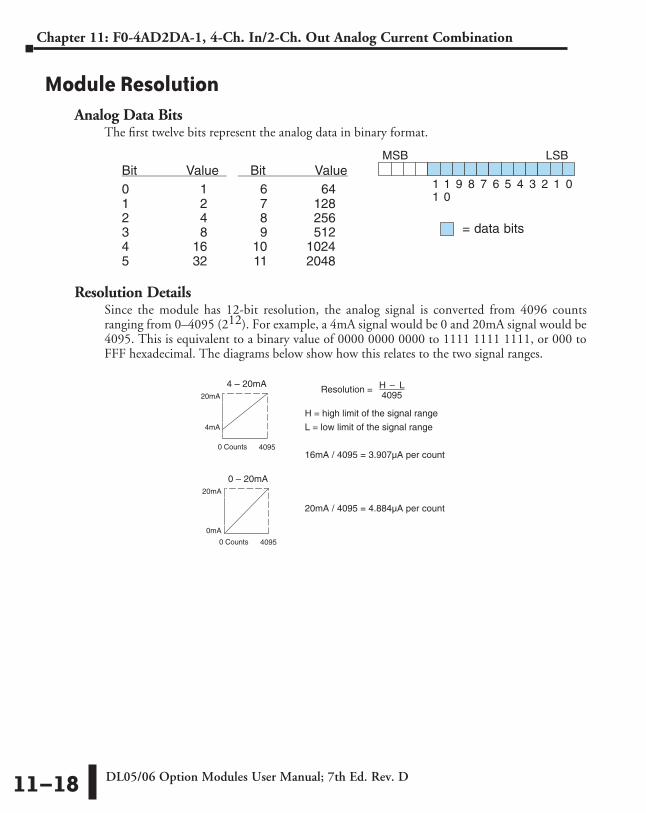
DL05/06 Option Modules User Manual; 7th Ed. Rev. D11–18
Chapter 11: F0-4AD2DA-1, 4-Ch. In/2-Ch. Out Analog Current Combination
Module ResolutionAnalog Data Bits
The first twelve bits represent the analog data in binary format.
Resolution DetailsSince the module has 12-bit resolution, the analog signal is converted from 4096 counts ranging from 0–4095 (212). For example, a 4mA signal would be 0 and 20mA signal would be 4095. This is equivalent to a binary value of 0000 0000 0000 to 1111 1111 1111, or 000 to FFF hexadecimal. The diagrams below show how this relates to the two signal ranges.
20mA
4mA
0 Counts 4095
4 – 20mAResolution = H – L
4095
H = high limit of the signal range
L = low limit of the signal range
16mA / 4095 = 3.907µA per count
20mA / 4095 = 4.884µA per count
20mA
0mA
0 Counts 4095
0 – 20mA
Bit Value Bit Value0 1 6 641 2 7 1282 4 8 2563 8 9 5124 16 10 10245 32 11 2048
MSB LSB
011
10
9 8 7 6 5 4 3 2 1
= data bits

DL05/06 Option Modules User Manual; 7th Ed. Rev. D 11–19
Chapter 11: F0-4AD2DA-1, 4-Ch. In/2-Ch. Out Analog Current Combination
Analog Input Ladder Logic FilterPID Loops / Filtering
Please refer to the “PID Loop Operation” chapter in the DL06 or DL05 User Manual for information on the built-in PV filter (DL05/06) and the ladder logic filter (DL06 only) shown below. A filter must be used to smooth the analog input value when auto tuning PID loops to prevent giving a false indication of loop characteristics.
Smoothing the Input Signal (DL06 only)The filter logic can also be used in the same way to smooth the analog input signal to help stabilize PID loop operation or to stabilize the analog input signal value for use with an operator interface display, etc.
WARNING: The built-in and logic filters are not intended to smooth or filter noise generated by improper field device wiring or grounding. Small amounts of electrical noise can cause the input signal to bounce considerably. Proper field device wiring and grounding must be done before attempting to use the filters to smooth the analog input signal.
Using Binary Data Format
LDDV2000
SUBRV1400
BTOR
SP1Loads the analog signal, which is in binary formatand has been loaded from V–memory locationV2000 – 2001, into the accumulator. Contact SP1is always on.
OUTDV1400
ADDRV1400
MULRR0.2
OUTV2100
RTOB
Converts the binary value in the accumulatorto a real number.
Subtracts the real number stored in locationV1400 from the real number in the accumulator,and stores the result in the accumulator. V1400is the designated workspace in this example.
Multiplies the real number in the accumulator by0.2 (the filter factor), and stores the result in the accumulator. This is the filtered value. The filterrange is 0.1 to 0.9. Smaller filter factorsincrease filtering. (1.0 eliminates filtering.)
Adds the real number stored in location V1400 to the real number filtered value in the accumulator, and stores the result in the accumulator.
Copies the value in the accumulator tolocation V1400.
Converts the real number in theaccumulator to a binary value, andstores the result in the accumulator.
Loads the binary number filtered value fromthe accumulator into location V2100 to use inyour application or PID loop.

DL05/06 Option Modules User Manual; 7th Ed. Rev. D11–20
Chapter 11: F0-4AD2DA-1, 4-Ch. In/2-Ch. Out Analog Current Combination
NOTE: Be careful not to do a multiple number conversion on a value. For example, if you are using the pointer method in BCD format to get the analog value, it must be converted to binary (BIN) as shown below. If you are using the pointer method in Binary format, the conversion to binary (BIN) instruction is not needed.
Using BCD Data Format
LDV2000
SUBRV1400
BTOR
SP1
BIN
OUTDV1400
ADDRV1400
MULRR0.2
OUTV1402
BCD
RTOB
Loads the analog signal, which is in BCD formatand has been loaded from V–memory locationV2000, into the accumulator. Contact SP1is always on.
Converts the BCD value in the accumulatorto binary.
Subtracts the real number stored in locationV1400 from the real number in the accumulator,and stores the result in the accumulator. V1400is the designated workspace in this example.
Multiplies the real number in the accumulator by0.2 (the filter factor), and stores the result in the accumulator. This is the filtered value. The filterrange is 0.1 to 0.9. Smaller filter factorsincrease filtering. (1.0 eliminates filtering.)
Adds the real number stored in location V1400 to the real number filtered value in the accumulator, and stores the result in the accumulator.
Copies the value in the accumulator tolocation V1400.
Converts the real number in theaccumulator to a binary value, andstores the result in the accumulator.
Loads the BCD number filtered value fromthe accumulator into location V1402 to use inyour application or PID loop.
Converts the binary value in the accumulator to a real number.
Converts the binary value in the accumulatorto a BCD number. Note: The BCD instruction is not needed to PID loop PV (loop PV is a binary number).
121212F0-2AD2DA-2 2-Ch. In/2-Ch. Out AnAlOg VOltAge COmbInAtIOn
ChapterChapterChapter
In This Chapter...Module Specifications .............................................................................................12–2
Setting the Module Jumpers ...................................................................................12–4
Connecting and Disconnecting the Field Wiring ...................................................12–5
Wiring Diagram .......................................................................................................12–5
Module Operation ...................................................................................................12–6
Special V-memory Locations ...................................................................................12–7
Using the Pointer in Your Control Program .........................................................12–10
Scale Conversions ..................................................................................................12–12
Module Resolution .................................................................................................12–15
Analog Input Ladder Logic Filter ..........................................................................12–16

DL05/06 Option Modules User Manual; 7th Ed. Rev. D12–2
Chapter 12: F0-2AD2DA-2 2-Ch. In/2-Ch. Out Analog Voltage Combination
Module SpecificationsThe F0-2AD2DA-2 Analog Combination module offers the following features: The analog input and output channels are updated in one scan.
• The module has a removable terminal block which makes it possible to remove the module without disconnecting the field wiring.
• Analog inputs can be used as process variables for the four (4) PID loops in the DL05 and the eight (8) PID loops in the DL06 CPUs.
• On-board active analog filtering and RISC-like microcontroller provide digital signal processing to maintain precise analog measurements in noisy environments.
NOTE: The DL05 CPU’s analog feature for this module requires DirectSOFT32 Version 3.0c (or later) and firmware version 3.30 (or later). The DL06 requires DirectSOFT32 version V4.0, build 16 (or later) and firmware version 1.00 (or later). See our website for more information: www.automationdirect.com.

DL05/06 Option Modules User Manual; 7th Ed. Rev. D 12–3
Chapter 12: F0-2AD2DA-2 2-Ch. In/2-Ch. Out Analog Voltage Combination
The following tables provide the specifications for the F0–2AD2DA–2 Analog Voltage Combination Module. Review these specifications to make sure the module meets your application requirements.
Input SpecificationsNumber of Channels 2, single ended (one common)Input Range 0 to 5VDC or 0 to 10VDC (jumper selectable)Resolution 12 bit (1 in 4096)Step Response 10.0 ms to 95% of full step changeCrosstalk 1/2 count maximum (-80db)*Active Low-pass Filtering -3dB at 300Hz (-12dB per octave)Input Impedance Greater than 20kq
Absolute Maximum Ratings ±15VLinearity Error (End to End) ±2 counts (0.025% of full scale) maximum*Input Stability ± 1 count *Gain Error ± 6 counts *Offset Error ± 2 counts *
Maximum Inaccuracy0.3% @ 25°C (77°F)0.6% 0 to 60°C (32 to 140°F)
Accuracy vs. Temperature ±100 ppm/°C typical
Output SpecificationsNumber of Channels 2, single ended (one common)Output Range 0 to 5VDC or 0 to 10VDC (jumper selectable)Resolution 12 bit (1 in 4096)Conversion Settling Time 50µS for full scale changeCrosstalk 1/2 count maximum (-80db) *Peak Output Voltage ±15VDC (power supply limited)Offset Error 0.1% of rangeGain Error 0.4% of rangeLinearity Error (end to end) ±1 count (0.075% of full scale) maximum*Output Stability ±2 counts*Load Impedance 2kq minimumLoad Capacitance 0.01 µF maximumAccuracy vs. Temperature ±50 ppm/°C typical* One count in the specification table is equal to one least significant bit of the analog data value (1 in 4096).

DL05/06 Option Modules User Manual; 7th Ed. Rev. D12–4
Chapter 12: F0-2AD2DA-2 2-Ch. In/2-Ch. Out Analog Voltage Combination
Setting the Module JumpersThe position of the J2 jumpers determines the input and output signal levels. You can choose between 0–5 VDC or 0–10 VDC. The module ships with the jumpers connecting the pins. In this position, the input and output signal level is 0–5 VDC. To select 0–10 VDC signals, use the jumper setting chart located on the module. One or more channels can be selected for 0–10 VDC input and output signal level by removing the jumper from the connecting pins of the appropriate channel. This will allow you to have one channel selected for a 0–5 VDC signal and another channel selected for a 0–10 VDC signal.
WARNING: Before removing the analog module or the terminal block on the face of the module, disconnect power to the PLC and all field devices. Failure to disconnect power can result in damage to the PLC and/or field devices.
ON=5V
CH
1
CH
2C
H1
CH
2
OUT INPUT
F0–2AD2DA–2
J2 (JUMPERS)
C20
J2, jumpers shown below, areconfigured as, CH1 INPUT andCH2 OUTPUT both set for 10V.CH2 INPUT and CH1 OUTPUTboth set for 5V.
Refer to jumper setting chart.
General Specifications
PLC Update Rate 2 input channels per scan 2 output channels per scan
16-bit Data Word 12 binary data bitsOperating Temperature 0 to 60° C (32 to 140° F)Storage Temperature -20 to 70° C (-4 to 158° F)Relative Humidity 5 to 95% (non-condensing)Environmental Air No corrosive gases permittedVibration MIL STD 810C 514.2Shock MIL STD 810C 516.2Noise Immunity NEMA ICS3-304Power Budget Requirement 50mA @ 5VDC (supplied by base)External Power Supply 30mA, 24VDC ±10%Connector Phoenix Mecano, Inc. Part No. AK1550/8-3.5 - greenConnector Wire Size 28–16 AWGConnector Screw Torque 3.5 inch-pounds (0.4 N·m)Connector Screwdriver Size DN-SS1 (recommended)

DL05/06 Option Modules User Manual; 7th Ed. Rev. D 12–5
Chapter 12: F0-2AD2DA-2 2-Ch. In/2-Ch. Out Analog Voltage Combination
Connecting and Disconnecting the Field WiringWiring Guidelines
Your company may have guidelines for wiring and cable installation. If so, you should check those before you begin the installation. Here are some general things to consider:
• Use the shortest wiring route whenever possible.
• Use shielded wiring and ground the shield at the transmitter source. Do not ground the shield at both the module and the source.
• Do not run the signal wiring next to large motors, high current switches, or transformers. This may cause noise problems.
• Route the wiring through an approved cable housing to minimize the risk of accidental damage. Check local and national codes to choose the correct method for your application.
The F0–2AD2DA–2 will require an external power supply with a rating of 18.0–26.4 VDC at 30mA.
To remove the terminal block, disconnect power to the PLC and the field devices. Pull the terminal block firmly until the connector separates from the module.
You can remove the analog module from the PLC by folding out the retaining tabs at the top and bottom of the module. As the retaining tabs pivot upward and outward, the module’s connector is lifted out of the PLC socket. Once the connector is free, you can lift the module out of its slot.
Wiring DiagramUse the following diagram to connect the field wiring. If necessary, the F0–2AD2DA–2 terminal block can be removed to make removal of the module possible without disturbing field wiring.
CH1
Transmitter
OV
A to DConverter
InternalModuleWiring
Analog S
witch
See NOTE 1
–
–
+
+
Typical User Wiring
+–
18.0–26.4VDCPower Supply
Module Supply
A n a lo g In/Out
NOTE 1: Shields should be grounded at the signalsource.
NOTE 2: Connect all external power supplycommons.
0–10V0–5V
2–In/2–Out
F0–2AD2DA–2
1IN2
1
2OUT
V+24V0V
0V
0V
Voltage4–wire
1
IN2
1
OUT2
0V
0V
V+24V0V
CH 1 load2k ohmsminimum
Resistance
CH 2 load2k ohmsminimum
Resistance
CH2
TransmitterVoltage2–wire
TransmitterPower Supply
–+
+
–
D to AConverter
D to AConverter
Ch 1
Voltage SourceCh 2
Voltage Source
NOTE: To ensure that readings on unused channels are zero, installa jumper between the CHx and COM terminals on all unused channels.
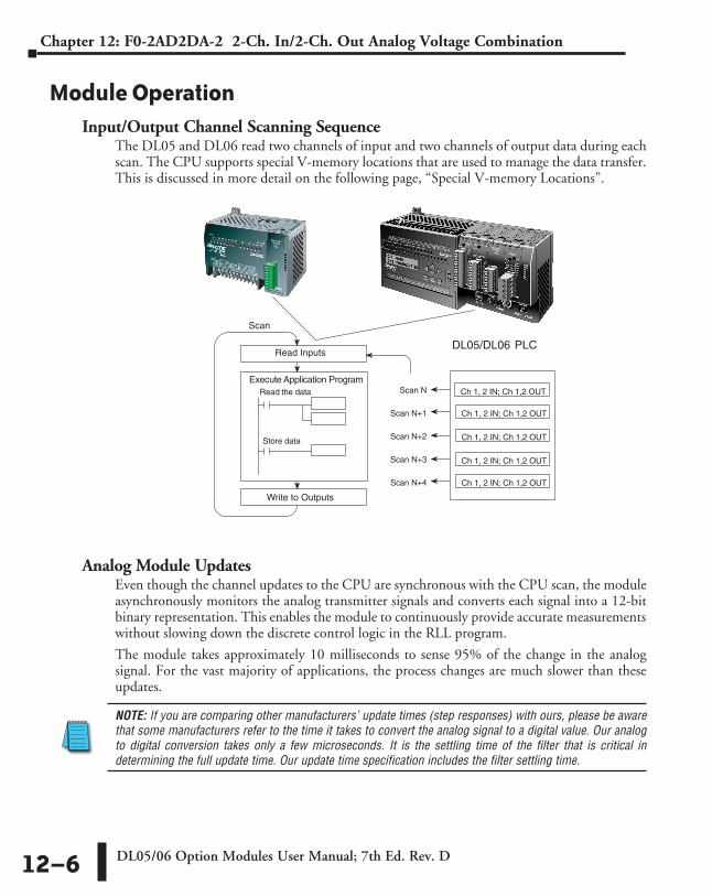
DL05/06 Option Modules User Manual; 7th Ed. Rev. D12–6
Chapter 12: F0-2AD2DA-2 2-Ch. In/2-Ch. Out Analog Voltage Combination
Module OperationInput/Output Channel Scanning Sequence
The DL05 and DL06 read two channels of input and two channels of output data during each scan. The CPU supports special V-memory locations that are used to manage the data transfer. This is discussed in more detail on the following page, “Special V-memory Locations”.
Analog Module UpdatesEven though the channel updates to the CPU are synchronous with the CPU scan, the module asynchronously monitors the analog transmitter signals and converts each signal into a 12-bit binary representation. This enables the module to continuously provide accurate measurements without slowing down the discrete control logic in the RLL program.
The module takes approximately 10 milliseconds to sense 95% of the change in the analog signal. For the vast majority of applications, the process changes are much slower than these updates.
NOTE: If you are comparing other manufacturers’ update times (step responses) with ours, please be aware that some manufacturers refer to the time it takes to convert the analog signal to a digital value. Our analog to digital conversion takes only a few microseconds. It is the settling time of the filter that is critical in determining the full update time. Our update time specification includes the filter settling time.
F2–
04A
D–1
, (L
)4-
Ch.
Cur
rent
Inp
ut
Read the data
Store data
Read Inputs
Execute Application Program
Scan
Write to Outputs
Ch 1, 2 IN; Ch 1,2 OUTScan N
Scan N+1
Scan N+2
Scan N+3
Scan N+4
DL05/DL06 PLC
Ch 1, 2 IN; Ch 1,2 OUT
Ch 1, 2 IN; Ch 1,2 OUT
Ch 1, 2 IN; Ch 1,2 OUT
Ch 1, 2 IN; Ch 1,2 OUT

DL05/06 Option Modules User Manual; 7th Ed. Rev. D 12–7
Chapter 12: F0-2AD2DA-2 2-Ch. In/2-Ch. Out Analog Voltage Combination
Special V-memory LocationsFormatting the Module Data
The DL05 and DL06 PLCs have three special V-memory locations assigned to their respective option slots These V-memory locations allow you to:
• Specify the data format (binary or BCD)
• Specify the number of I/O channels to scan (2 input and 2 output channels for the F0–2AD2DA–2)
• Specify the V-memory locations to store the input data
• Specify the V-memory locations to store the output data
DL05 Data FormattingThe table below shows the special V-memory locations used by the DL05 PLC for the analog combination modules.
Structure of V7700V-memory location 7700 is used for identifying the number of output channels, the number of input channels and the data type (binary or BCD). The low byte equals the number of output channels and the high byte equals the number of input channels. Either a 1 or a 2 will be entered to select the number of input and output channels to be used. A zero (0) entered for channel selection will cause the channel, either input or output, to be inoperative.
Loading a constant of 202 into V7700 identifies two input and two output analog channels, and sets the I/O data type to BCD.
Loading a constant of 8282 into V7700 identifies two input and two output analog channels, and sets the I/O data type to binary.
Structure of V7701V7701 is a system parameter that points to a V-memory location used for storing analog input data. The V-memory location loaded in V7701 is an octal number identifying the first V-memory location for the analog input data. This V-memory location is user selectable. For example, loading O2000, using the LDA instruction,causes the pointer to write Ch 1’s data value to V2000 and Ch 2’s data value to V2001.
Analog Combination Module DL05 Special V-memory Locations
Data Type and Number of I/O Channels V7700Input Storage Pointer V7701Output Storage Pointer V7702
MSB LSB
LOW BYTE
MSB LSB
HIGH BYTE

DL05/06 Option Modules User Manual; 7th Ed. Rev. D12–8
Chapter 12: F0-2AD2DA-2 2-Ch. In/2-Ch. Out Analog Voltage Combination
Structure of V7702V7702 is a system parameter that points to a V-memory location used for storing analog output data. The V-memory location loaded in V7702 is an octal number identifying the first V-memory location for the analog output data. This V-memory location is user selectable. For example, loading O2010, using the LDA instruction, causes the pointer to write Ch 1’s data value from V2010 and Ch 2’s data value from V2011.
You will find an example program that loads appropriate values to V7700, V7701 and V7702 on page 12–10.

DL05/06 Option Modules User Manual; 7th Ed. Rev. D 12–9
Chapter 12: F0-2AD2DA-2 2-Ch. In/2-Ch. Out Analog Voltage Combination
DL06 Data FormattingSpecial V-memory locations are assigned to the four option module slots of the DL06 PLC. The table below shows these V-memory locations which can be used by the F0–2AD2DA–2.
Setup Data Type and Number of ChannelsV-memory locations 700, 710, 720 and 730 are used for identifying the number of output channels, the number of input channels and the data type (binary or BCD). The low byte equals the number of output channels and the high byte equals the number of input channels. Enter a 1 or 2 to select the number of input and output channels to be used. A zero (0) entered for channel selection will cause the channel, either input or output, to be inoperative.
For example, with a module installed in slot 1 by loading a constant of 202 into V700 identifies two input and two output analog channels, and sets the I/O data type to BCD.
And, loading a constant of 8282 into V700 identifies two input and two output analog channels, and sets the I/O data type to binary.
Input Storage PointerV-memory locations 701, 711, 721 and 731 are special locations used as a storage pointers for the analog input data. With the analog module installed in slot 1, the V-memory location loaded in V701 is an octal number identifying the first user V-memory location to read the analog input data. This V-memory location is user selectable. For example, loading O2000, using the LDA instruction, causes the pointer to write Ch 1’s data value to V2000 and Ch 2’s data value to V2001.
Output Storage PointerV-memory locations 702, 712, 722 and 732 are special locations used as storage pointer for the analog output data. With the analog module installed in slot 1, the V-memory location loaded in V702 is an octal number identifying the first user V-memory location to write the analog output data to. This V-memory location is user selectable. For example, loading O2010, using the LDA instruction, causes the pointer to write Ch 1’s data value from V2010 and Ch 2’s data value from V2011.
You will find an example program that loads appropriate values to V700, V701 and V702 on page 12–11.
Analog Combination Module DL06 Special V-memory Locations
Slot No. 1 2 3 4Number of Channels V700 V710 V720 V730Input Pointer V701 V711 V721 V731Output Pointer V702 V712 V722 V732
MSB LSB
LOW BYTE
MSB LSB
HIGH BYTE

DL05/06 Option Modules User Manual; 7th Ed. Rev. D12–10
Chapter 12: F0-2AD2DA-2 2-Ch. In/2-Ch. Out Analog Voltage Combination
Using the Pointer in Your Control ProgramDL05 Pointer Method
The DL05 CPU examines the pointer values (the memory locations identified in V7700, V7701 and V7702) on the first scan only.
The example program below shows how to setup these locations for 2 input channels and 2 output channels. This rung can be placed anywhere in the ladder program or in the initial stage if you are using stage programming instructions.
This is all that is required to read the analog input data into V-memory locations. Once the data is in V-memory you can perform mathematical calculations with the data, compare the data against preset values, and so forth. V2000 and V2010 is used in the example but you can use any user V-memory location.
LD
SP0LD
LDAO2000
OUTV7701
This loads an octal value for the first V-memory location that will be usedto store the incoming data. For example, the O2000 entered here usingthe LDA instruction would designate the following addresses: Ch1 –V2000, Ch2 – V2001
The octal address (O2000) is stored here. V7701 is assigned to theoption slot and acts as a pointer, which means the CPU will use theoctal value in this location to determine exactly where to store theincoming data.
OUTV7700
Special V-memory location assigned to the option slot contains the dataformat and the number of channels to scan.
Load a constant that specifies the number of channels to scan and thedata format. The upper byte selects the input data format (i.e. 0=BCD,8=Binary) and the number of input channels (set to either 1 or 2 for theF0–2AD2DA–2). The lower byte selects the output data format (i.e.0=BCD, 8=Binary) and the number of output channels (set to either 1or 2).
- or -
The binary format is used for displaying data on some operatorinterface units. The DL05 PLCs support binary math functions.
LDAO2010
OUTV7702
This loads an octal value for the first V-memory location that will be usedto store the output data. For example, the O2010 entered here using theLDA instruction would designate the following addresses: Ch1 – V2010,Ch2 – V2011
The octal address (O2010) is stored here. V7702 is assigned to theoption slot and acts as a pointer , which means the CPU will use theoctal value in this location to determine exactly where to store the outputdata.
K202
K8282
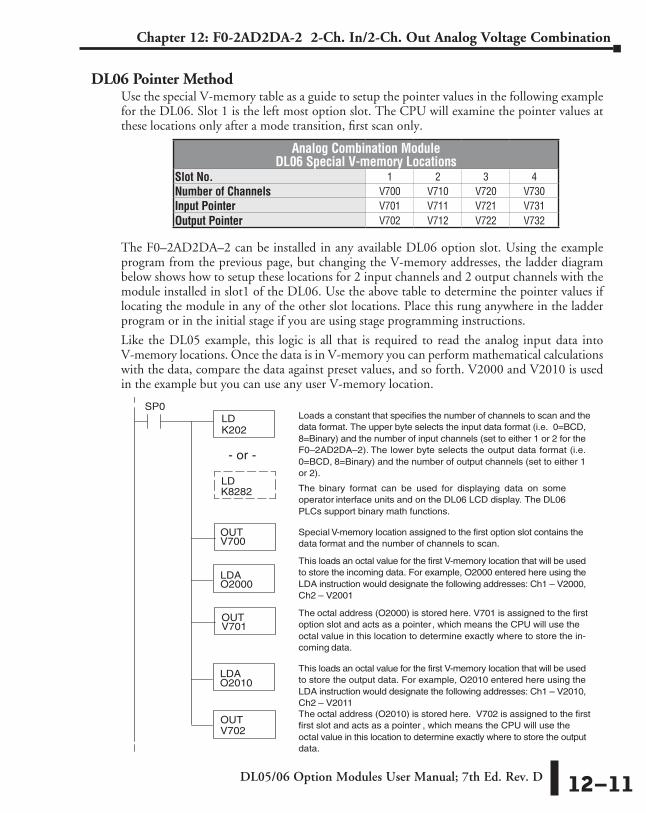
DL05/06 Option Modules User Manual; 7th Ed. Rev. D 12–11
Chapter 12: F0-2AD2DA-2 2-Ch. In/2-Ch. Out Analog Voltage Combination
DL06 Pointer MethodUse the special V-memory table as a guide to setup the pointer values in the following example for the DL06. Slot 1 is the left most option slot. The CPU will examine the pointer values at these locations only after a mode transition, first scan only.
The F0–2AD2DA–2 can be installed in any available DL06 option slot. Using the example program from the previous page, but changing the V-memory addresses, the ladder diagram below shows how to setup these locations for 2 input channels and 2 output channels with the module installed in slot1 of the DL06. Use the above table to determine the pointer values if locating the module in any of the other slot locations. Place this rung anywhere in the ladder program or in the initial stage if you are using stage programming instructions.
Like the DL05 example, this logic is all that is required to read the analog input data into V-memory locations. Once the data is in V-memory you can perform mathematical calculations with the data, compare the data against preset values, and so forth. V2000 and V2010 is used in the example but you can use any user V-memory location.
F0–2AD
2DA
–2
LD
SP0LD
LDAO2000
OUTV701
This loads an octal value for the first V-memory location that will be usedto store the incoming data. For example, O2000 entered here using theLDA instruction would designate the following addresses: Ch1 – V2000,Ch2 – V2001
The octal address (O2000) is stored here. V701 is assigned to the firstoption slot and acts as a pointer, which means the CPU will use theoctal value in this location to determine exactly where to store the in-coming data.
OUTV700
Special V-memory location assigned to the first option slot contains thedata format and the number of channels to scan.
Loads a constant that specifies the number of channels to scan and the data format. The upper byte selects the input data format (i.e. 0=BCD,8=Binary) and the number of input channels (set to either 1 or 2 for theF0–2AD2DA–2). The lower byte selects the output data format (i.e.0=BCD, 8=Binary) and the number of output channels (set to either 1or 2).
- or -
The binary format can be used for displaying data on someoperator interface units and on the DL06 LCD display. The DL06PLCs support binary math functions.
LDAO2010
OUTV702
This loads an octal value for the first V-memory location that will be usedto store the output data. For example, O2010 entered here using theLDA instruction would designate the following addresses: Ch1 – V2010,Ch2 – V2011The octal address (O2010) is stored here. V702 is assigned to the firstfirst slot and acts as a pointer , which means the CPU will use theoctal value in this location to determine exactly where to store the outputdata.
K202
K8282
Analog Combination Module DL06 Special V-memory Locations
Slot No. 1 2 3 4Number of Channels V700 V710 V720 V730Input Pointer V701 V711 V721 V731Output Pointer V702 V712 V722 V732

DL05/06 Option Modules User Manual; 7th Ed. Rev. D12–12
Chapter 12: F0-2AD2DA-2 2-Ch. In/2-Ch. Out Analog Voltage Combination
Scale ConversionsScaling the Input Data
Many applications call for measurements in engineering units, which can be more meaningful than raw data. Convert to engineering units using the formula shown to the right.
You may have to make adjustments to the formula depending on the scale you choose for the engineering units.
For example, if you wanted to measure pressure (PSI) from 0.0 to 100.0 then you would have to multiply the analog value by 10 in order to imply a decimal place when you view the value with the programming software or a handheld programmer. Notice how the calculations differ when you use the multiplier.
Analog Value of 2024, slightly less than half scale, should yield 49.4 PSI.
Units = A H – L4095
H = High limit of the engineeringunit range
L = Low limit of the engineering unit range
A = Analog value (0 – 4095)
+ L
Units = A H – L4095
Example without multiplier Example with multiplier
Units = 2024 100 – 04095
Units = 49
Units = 10 A H – L 4095
Units = 20240 100 – 0 4095
Units = 494
+ L
+ 0
+ L
+ 0
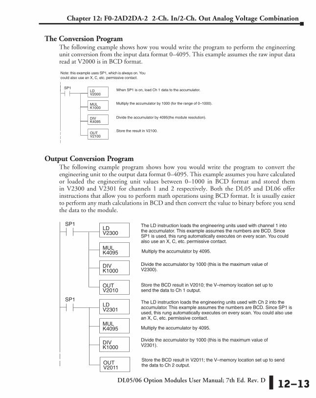
DL05/06 Option Modules User Manual; 7th Ed. Rev. D 12–13
Chapter 12: F0-2AD2DA-2 2-Ch. In/2-Ch. Out Analog Voltage Combination
The Conversion ProgramThe following example shows how you would write the program to perform the engineering unit conversion from the input data format 0–4095. This example assumes the raw input data read at V2000 is in BCD format.
Output Conversion ProgramThe following example program shows how you would write the program to convert the engineering unit to the output data format 0–4095. This example assumes you have calculated or loaded the engineering unit values between 0–1000 in BCD format and stored them in V2300 and V2301 for channels 1 and 2 respectively. Both the DL05 and DL06 offer instructions that allow you to perform math operations using BCD format. It is usually easier to perform any math calculations in BCD and then convert the value to binary before you send the data to the module.
LDV2000
SP1
MULK1000
DIVK4095
When SP1 is on, load Ch 1 data to the accumulator.
Multiply the accumulator by 1000 (for the range of 0–1000).
Divide the accumulator by 4095(the module resolution).
OUTV2100
Store the result in V2100.
Note: this example uses SP1, which is always on. Youcould also use an X, C, etc. permissive contact.
The LD instruction loads the engineering units used with channel 1 intothe accumulator. This example assumes the numbers are BCD. SinceSP1 is used, this rung automatically executes on every scan. You couldalso use an X, C, etc. permissive contact.
LDV2300
SP1
MULK4095
DIVK1000
Multiply the accumulator by 4095.
Divide the accumulator by 1000 (this is the maximum value ofV2300).
OUTV2010
Store the BCD result in V2010; the V–memory location set up tosend the data to Ch 1 output.
The LD instruction loads the engineering units used with Ch 2 into theaccumulator. This example assumes the numbers are BCD. Since SP1 isused, this rung automatically executes on every scan. You could also usean X, C, etc. permissive contact.
LDV2301
SP1
MULK4095
DIVK1000
Multiply the accumulator by 4095.
Divide the accumulator by 1000 (this is the maximum value ofV2301).
OUTV2011
Store the BCD result in V2011; the V–memory location set up to sendthe data to Ch 2 output.

DL05/06 Option Modules User Manual; 7th Ed. Rev. D12–14
Chapter 12: F0-2AD2DA-2 2-Ch. In/2-Ch. Out Analog Voltage Combination
Analog and Digital Value ConversionsSometimes it is useful to convert between the signal levels and the digital values. This is especially helpful during machine startup or troubleshooting. The following table provides formulas to make this conversion easier.
For example, if you are using the 0–10V range and you need a 6V signal level, use this formula to determine the digital value (D) that will be stored in the V-memory location that contains the data.
D = 409510
(A)
D = 409510
(6V)
D = (409.5) (6) D = 2457
Range If you know the digital value If you know the analog signal level
0 to 5V A = 5D 4095
D = 4095 (A) 5
0 to 10V A = 10D 4095
D = 4095 (A) 10

DL05/06 Option Modules User Manual; 7th Ed. Rev. D 12–15
Chapter 12: F0-2AD2DA-2 2-Ch. In/2-Ch. Out Analog Voltage Combination
Module ResolutionAnalog Data Bits
The first twelve bits represent the analog data for both inputs and outputs in binary format.
Resolution DetailsSince the module has 12-bit resolution for both inputs and outputs, the analog signal is either converted into 4096 counts or a count value will produce a proportional analog output. In either situation the count range will be from 0–4095 (212). For example, with an output range of 0 to 10V, send a 0 to get a 0V signal, and send 4095 to get a 10V signal. This is equivalent to a binary value of 0000 0000 0000 to 1111 1111 1111, or 000 to FFF hexadecimal.
Each count can also be expressed in terms of the signal level by using the following equation:
The following table shows the smallest detectable signal change that will result in one LSB change in the data or the amount of change in the output signal that each increment of the count value will produce.
Bit Value Bit Value0 1 6 641 2 7 1282 4 8 2563 8 9 5124 16 10 10245 32 11 2048
MSB LSB
011
10
9 8 7 6 5 4 3 2 1
= data bits
10V
0V0 4095
0 – 10VResolution = H – L
4095
H = high limit of the signal range
L = low limit of the signal range
Voltage Range Signal Span Divide By Smallest detectable or Produced Change
0 to 5V 5 volts 4095 1.22 mV0 to 10V 10 volts 4095 2.44 mV

DL05/06 Option Modules User Manual; 7th Ed. Rev. D12–16
Chapter 12: F0-2AD2DA-2 2-Ch. In/2-Ch. Out Analog Voltage Combination
Analog Input Ladder Logic FilterPID Loops / Filtering
Please refer to the “PID Loop Operation” chapter in the DL06 or DL05 User Manual for information on the built-in PV filter (DL05/06) and the ladder logic filter (DL06 only) shown below. A filter must be used to smooth the analog input value when auto tuning PID loops to prevent giving a false indication of loop characteristics.
Smoothing the Input Signal (DL06 only)The filter logic can also be used in the same way to smooth the analog input signal to help stabilize PID loop operation or to stabilize the analog input signal value for use with an operator interface display, etc.
WARNING: The built-in and logic filters are not intended to smooth or filter noise generated by improper field device wiring or grounding. Small amounts of electrical noise can cause the input signal to bounce considerably. Proper field device wiring and grounding must be done before attempting to use the filters to smooth the analog input signal.
Using Binary Data Format
LDV2000
SUBRV1400
BTOR
SP1Loads the analog signal, which is in binary formatand has been loaded from V-memory locationV2000, into the accumulator. Contact SP1 isalways on.
Converts the binary value in the accumulatorto a real number.
Subtracts the real number stored in locationV1400 from the real number in the accumulator,and stores the result in the accumulator. V1400is the designated workspace in this example.
Multiplies the real number in the accumulator by0.2 (the filter factor), and stores the result in theaccumulator. This is the filtered value. The filterrange is 0.1 to 0.9. Smaller filter factorsincreases filtering. (1.0 eliminates filtering).
OUTDV1400
ADDRV1400
MULRR0.2
OUTV1402
RTOB
Adds the real number stored inlocation V1400 to the real numberfiltered value in the accumulator, andstores the result in the accumulator.
Copies the value in the accumulator tolocation V1400.
Converts the real number in theaccumulator to a binary value, andstores the result in the accumulator.
Loads the binary number filtered value fromthe accumulator into location V1402 to use inyour application or PID loop.

DL05/06 Option Modules User Manual; 7th Ed. Rev. D 12–17
Chapter 12: F0-2AD2DA-2 2-Ch. In/2-Ch. Out Analog Voltage Combination
NOTE: Be careful not to do a multiple number conversion on a value. For example, if you are using the pointer method in BCD format to get the analog value, it must be converted to binary (BIN) as shown below. If you are using the pointer method in Binary format, the conversion to binary (BIN) instruction is not needed.
Using BCD Data Format
LDDV2000
SUBRV1400
BTOR
SP1
BIN
Loads the analog signal, which is in BCD formatand has been loaded from V-memory locationV2000, into the accumulator. Contact SP1 isalways on.
Converts a BCD value in the accumulator tobinary.
Converts the binary value in the accumulatorto a real number.
Subtracts the real number stored in locationV1400 from the real number in the accumulator,and stores the result in the accumulator. V1400is the designated workspace in this example.
Multiplies the real number in the accumulator by0.2 (the filter factor), and stores the result in theaccumulator. This is the filtered value. The filterrange is 0.1 to 0.9. Smaller filter factorsincreases filtering. (1.0 eliminates filtering).
OUTDV1400
ADDRV1400
MULRR0.2
OUTDV1402
BCD
RTOB
Adds the real number stored inlocation V1400 to the real numberfiltered value in the accumulator, andstores the result in the accumulator.
Copies the value in the accumulator tolocation V1400.
Converts the real number in theaccumulator to a binary value, andstores the result in the accumulator.
Converts the binary value in the accumulatorto a BCD number. Note: The BCD instructionis not needed for PID loop PV (loop PV is abinary number).
Loads the BCD number filtered value fromthe accumulator into location V1402 to use inyour application or PID loop.

131313F0-4AD2DA-2, 4-Ch. In/2-Ch. Out AnAlOg VOltAge COmbInAtIOn
ChapterChapterChapter
In This Chapter...Module Specifications .............................................................................................13–2
Setting the Module Jumpers ...................................................................................13–4
Connecting and Disconnecting the Field Wiring ...................................................13–5
Wiring Diagram .......................................................................................................13–5
Module Operation ...................................................................................................13–6
Special V-memory Locations ...................................................................................13–7
Using the Pointer in Your Control Program .........................................................13–10
Scale Conversions ..................................................................................................13–12
Module Resolution .................................................................................................13–15
Analog Input Ladder Logic Filter ..........................................................................13–16

DL05/06 Option Modules User Manual; 7th Ed. Rev. D13–2
Chapter 13: F0-4AD2DA-2, 4-Ch. In/2 Ch. Out Analog Voltage Combination
Module SpecificationsThe F0-4AD2DA-2 Analog Combination module offers the following features:
• The analog input and output channels are updated in one scan.
• The removable terminal block makes it possible to remove the module without disconnecting the field wiring.
• Analog inputs can be used as process variables for the four (4) PID loops in the DL05 CPU and the eight (8) PID loops in the DL06 CPUs.
• On-board active analog filtering and RISC-like microcontroller provide digital signal processing to maintain precise analog measurements in noisy environments.
NOTE: The DL05 CPU’s analog feature for this module requires DirectSOFT32 Version 3.0c (or later) and firmware version 3.30 (or later). The DL06 requires DirectSOFT32 version V4.0, build 16 (or later) and firmware version 1.00 (or later). See our website for more information: www.automationdirect.com.

DL05/06 Option Modules User Manual; 7th Ed. Rev. D 13–3
Chapter 13: F0-4AD2DA-2, 4-Ch. In/2 Ch. Out Analog Voltage Combination
The following tables provide the specifications for the F0–4AD2DA–2 Analog Combination Module. Review these specifications to make sure the module meets your application requirements.
Input SpecificationsNumber of Channels 4, single ended (one common)Input Range 0 to 5VDC or 0 to 10VDC (jumper selectable)Resolution 12 bit (1 in 4096)Step Response 10.0 ms to 95% of full step changeCrosstalk -80dB, 1/2 count maximum*Active Low-pass Filtering -3dB at 300Hz (-12dB per octave)Input Impedance Greater than 20kq
Absolute Maximum Ratings ±15VLinearity Error (End to End) ±2 counts maximum*Input Stability ±1 count*Gain Error ±6 counts maximum*Offset Error ±2 counts maximum*
Maximum Inaccuracy±0.3% @ 25°C (77°F)±0.6% 0 to 60°C (32 to 140°F)
Accuracy vs. Temperature ±100 ppm/°C typical
Output SpecificationsNumber of Channels 2, single ended (one common)Output Range 0 to 5 VDC or 0 to 10 VDC (jumper selectable)Resolution 12 bit (1 in 4096)Conversion Settling Time 50µS for full scale changeCrosstalk -80db, 1/2 count maximum*Peak Output Voltage ±15VDC (power supply limited)Offset Error 0.1% of rangeGain Error 0.4% of rangeLinearity Error (end to end) ±1 count (0.075% of full scale) maximum*Output Stability ±2 counts*Load Impedance 2kq maximumLoad Capacitance 0.01 µF maximumAccuracy vs. Temperature ±50 ppm/°C typical* One count in the specification table is equal to one least significant bit of the analog data value (1 in 4096).
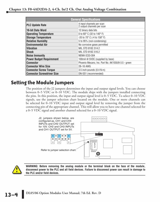
DL05/06 Option Modules User Manual; 7th Ed. Rev. D13–4
Chapter 13: F0-4AD2DA-2, 4-Ch. In/2 Ch. Out Analog Voltage Combination
Setting the Module JumpersThe position of the J2 jumpers determines the input and output signal levels. You can choose between 0–5 VDC or 0–10 VDC. The module ships with the jumpers installed connecting the pins. In this position, the input and output signal level is 0–5 VDC. To select 0–10 VDC signals, use the jumper selection chart located on the module. One or more channels can be selected for 0–10 VDC input and output signal level by removing the jumper from the connecting pin of the appropriate channel. This will allow you to have one channel selected for a 0–5 VDC signal and another channel selected for a 0–10 VDC signal.
WARNING: Before removing the analog module or the terminal block on the face of the module, disconnect power to the PLC and all field devices. Failure to disconnect power can result in damage to the PLC and/or field devices.
CH
1C
H2
CH
1C
H2
C14
CH
3C
H4
INP
UT
S
OU
TP
UT
S
ON=0–5VRANGE
J2
J2, jumpers shown below, areconfigured as, CH1 and CH4 INPUTs and CH2 OUTPUT setfor 10V. CH2 and CH3 INPUTsand CH1 OUTPUT set for 5V.
Refer to jumper selection chart.
General Specifications
PLC Update Rate 4 input channels per scan 2 output channels per scan
16-bit Data Word 12 binary data bitsOperating Temperature 0 to 60° C (32 to 140° F)Storage Temperature -20 to 70° C (-4 to 158° F)Relative Humidity 5 to 95% (non-condensing)Environmental Air No corrosive gases permittedVibration MIL STD 810C 514.2Shock MIL STD 810C 516.2Noise Immunity NEMA ICS3-304Power Budget Requirement 100mA @ 5VDC (supplied by base)Connector Phoenix Mecano, Inc. Part No. AK1550/8-3.5 - greenConnector Wire Size 28–16 AWGConnector Screw Torque 3.5 inch-pounds (0.4 N·m)Connector Screwdriver Size DN-SS1 (recommended)

DL05/06 Option Modules User Manual; 7th Ed. Rev. D 13–5
Chapter 13: F0-4AD2DA-2, 4-Ch. In/2 Ch. Out Analog Voltage Combination
Connecting and Disconnecting the Field WiringWiring Guidelines
Your company may have guidelines for wiring and cable installation. If so, you should check those before you begin the installation. Here are some general things to consider:
• Use the shortest wiring route whenever possible.
• Use shielded wiring and ground the shield at the transmitter source. Do not ground the shield at both the module and the source.
• Do not run the signal wiring next to large motors, high current switches, or transformers. This may cause noise problems.
• Route the wiring through an approved cable housing to minimize the risk of accidental damage. Check local and national codes to choose the correct method for your application.
A separate transmitter power supply may be required, depending on the type of transmitter being used. This module has a removable connector to make wiring and module removal easier. To remove the terminal block, disconnect power to the PLC and the field devices. Pull the terminal block firmly until the connector separates from the module.
The analog module can be removed from the PLC by folding out the retaining tabs at the top and bottom of the module. As the retaining tabs pivot upward and outward, the module’s connector is lifted out of the PLC socket. Once the connector is free, you can lift the module out of its slot.
Wiring DiagramUse the following diagram to connect the field wiring. If necessary, the terminal block can be removed to make removal of the module possible without disturbing field wiring.
CH1
Transmitter
OV
A to DConverter
InternalModuleWiring
Analog S
witch
See NOTE 1
–
–
+
+
A n a lo g In/Out
0–10V0–5V
4–In/2–Out
F0–4AD2DA–2
1
IN
2
1
2
OUT
0V
Voltage2–wire
1
IN
2
1
OUT
2
0V
0V
CH 1 load2k ohmsminimum
Resistance
CH 2 load2k ohmsminimum
Resistance
CH2
TransmitterVoltage2–wire
3
4
–
–
+
+
CH3
TransmitterVoltage4–wire
CH4
TransmitterVoltage3–wire 3
4
0V
Typical User Wiring
TransmitterPower Supply
–
–
+
+
+
NOTE 1: Shields should be grounded at the signalsource.
NOTE 2: Connect all external power supplycommons.
D to AConverter
D to AConverter
Ch 1
Voltage SourceCh 2
Voltage Source
NOTE 3: To ensure that readings on unused channels are zero, installa jumper between the CHx and COM terminals on all unused channels.

DL05/06 Option Modules User Manual; 7th Ed. Rev. D13–6
Chapter 13: F0-4AD2DA-2, 4-Ch. In/2 Ch. Out Analog Voltage Combination
Module OperationInput/Output Channel Update Sequence
The DL05 and DL06 read four channels of input data and two channels of output data during each scan. The CPU supports special V-memory locations that are used to manage the data transfer. This is discussed in more detail on the next page, “Special V-memory Locations”.
Analog Module UpdatesEven though the channel updates to the CPU are synchronous with the CPU scan, the module asynchronously monitors the analog transmitter signals and converts each signal into a 12-bit binary representation. This enables the module to continuously provide accurate measurements without slowing down the discrete control logic in the RLL program.
The module takes approximately 10 milliseconds to sense 95% of the change in the analog signal. For the vast majority of applications, the process changes are much slower than these updates.
NOTE: If you are comparing other manufacturers’ update times (step responses) with ours, please be aware that some manufacturers refer to the time it takes to convert the analog signal to a digital value. Our analog to digital conversion takes only a few microseconds. It is the settling time of the filter that is critical in determining the full update time. Our update time specification includes the filter settling time.
Read the data
Store data
Read Inputs
Execute Application Program
Scan
Write to Outputs
Ch 1, 2, 3, 4 IN; Ch 1,2 OUTScan N
Scan N+1
Scan N+2
Scan N+3
Scan N+4
DL05/DL06 PLC
Ch 1, 2, 3, 4 IN; Ch 1,2 OUT
Ch 1, 2, 3, 4 IN; Ch 1,2 OUT
Ch 1, 2, 3, 4 IN; Ch 1,2 OUT
Ch 1, 2, 3, 4 IN; Ch 1,2 OUT

DL05/06 Option Modules User Manual; 7th Ed. Rev. D 13–7
Chapter 13: F0-4AD2DA-2, 4-Ch. In/2 Ch. Out Analog Voltage Combination
Special V-memory LocationsFormatting the Module Data
The DL05 and DL06 PLCs have three special V-memory locations assigned to their respective option slots. These V-memory locations allow you to:
• Specify the data format (binary or BCD)
• Specify the number of input and output channels to scan.
• Specify the V-memory locations to store the input data
• Specify the V-memory locations to store the output data
DL05 Data FormattingThe table below shows the special V-memory locations which are used by the DL05 PLC for the F0–4AD2DA–2.
Structure of V7700V-memory location 7700 is used for identifying the number of output channels, the number of input channels and the data type (binary or BCD). The low byte equals the number of output channels and the high byte equals the number of input channels. Enter a 1 through 4 to select the number of input channels and a 1 through 2 to select the number of output channels to be used. A zero (0) entered for channel selection will cause the channel, either input or output, to be inoperative.
Loading a constant of 402 into V7700 identifies four input and two output analog channels, and sets the I/O data type to BCD.
Loading a constant of 8482 into V7700 identifies four input and two output analog channels, and sets the I/O data type to binary.
Structure of V7701V7701 is a system parameter that points to a V-memory location used for storing analog input data. The V-memory location loaded in V7701 is an octal number identifying the first V-memory location for the analog input data. This V-memory location is user selectable. For example, loading O2000 using the LDA instruction causes the pointer to write Ch 1’s data value to V2000, Ch 2’s data value to V2001, CH 3’s data value to V2002 and Ch 4’s data value to V2003.
Analog Combination Module DL05 Special V-memory Locations
Data Type and Number of I/O Channels V7700Input Storage Pointer V7701Output Storage Pointer V7702
MSB LSB
LOW BYTE
MSB LSB
HIGH BYTE

DL05/06 Option Modules User Manual; 7th Ed. Rev. D13–8
Chapter 13: F0-4AD2DA-2, 4-Ch. In/2 Ch. Out Analog Voltage Combination
Structure of V7702V7702 is a system parameter that points to a V-memory location used for storing analog output data. The V-memory location loaded in V7702 is an octal number identifying the first V-memory location for the analog output data. This V-memory location is user selectable. For example, loading O2010 using the LDA instruction causes the pointer to read Ch 1’s data value at V2010 and Ch 2’s data value at V2011.
You will find an example program that loads appropriate values to V7700, V7701 and V7702 on page 13–10.

DL05/06 Option Modules User Manual; 7th Ed. Rev. D 13–9
Chapter 13: F0-4AD2DA-2, 4-Ch. In/2 Ch. Out Analog Voltage Combination
DL06 Data FormattingSpecial V-memory locations are assigned to the four option module slots of the DL06 PLC. The table below shows these V-memory locations which can be used for the F0–4AD2DA–2.
Setup Data Type and Number of ChannelsV-memory location 700, 710, 720 and 730 are used for identifying the number of output channels, the number of input channels and the data type (binary or BCD). The low byte equals the number of output channels and the high byte equals the number of input channels. Enter a 1 through 4 to select the number of input channels and a 1 or 2 to select the number of output channels to be used. A zero (0) entered for channel selection will cause the channel, either input or output, to be inoperative.
For example, with a module installed in slot 4 by loading a constant of 402 into V730 identifies four input and two output analog channels, and sets the I/O data type to BCD.
Or, loading a constant of 8482 into V730 identifies four input and two output analog channels, and sets the I/O data type to binary.
Input Storage Pointer SetupV-memory locations 701, 711, 721 and 731 are special locations used as storage pointers for the analog input data. With the analog module installed in slot 4, the V-memory location loaded in V731, for instance, is an octal number identifying the first user V-memory location to read the analog input data. This V-memory location is user selectable. For example, loading O2000 using the LDA instruction causes the pointer to write Ch 1’s data value to V2000, Ch 2’s data value to V2001, CH 3’s data value to V2002 and Ch 4’s data value to V2003.
Output Storage Pointer SetupV-memory locations 702, 712, 722 and 732 are special locations used as storage pointers for the analog output data. With the analog module installed in slot 4, the V-memory location loaded in V732 is an octal number identifying the first user V-memory location to write the analog output data to. This V-memory location is user selectable. For example, loading O2010 using the LDA instruction causes the pointer to read Ch 1’s data value at V2010 and Ch 2’s data value at V2011.
You will find an example program that loads appropriate values to V700, V701 and V702 on page 13–11.
Analog Combination Module DL06 Special V-memory Locations
Slot No. 1 2 3 4Number of Channels V700 V710 V720 V730Input Pointer V701 V711 V721 V731Output Pointer V702 V712 V722 V732
MSB LSB
LOW BYTE
MSB LSB
HIGH BYTE

DL05/06 Option Modules User Manual; 7th Ed. Rev. D13–10
Chapter 13: F0-4AD2DA-2, 4-Ch. In/2 Ch. Out Analog Voltage Combination
Using the Pointer in Your Control ProgramDL05 Pointer Method
The DL05 CPU examines the pointer values (the memory locations identified in V7700, V7701 and V7702) on the first scan only.
The example program below shows how to setup these locations for 4 input channels and 2 output channels. This rung can be placed anywhere in the ladder program or in the initial stage if you are using stage programming instructions.
This is all that is required to read the analog input data into V-memory locations. Once the data is in V-memory you can perform math on the data, compare the data against preset values, and so forth. V2000 and V2010 is used in the example but you can use any user V-memory location.
SP0LD
LDAO2000
OUTV7701
This loads an octal value for the first V-memory location that will be usedto store the incoming data. For example, the O2000 entered here woulddesignate the following addresses:Ch1 – V2000, Ch2 – V2001, Ch3 – V2002, Ch4 – V2003
The octal address (O2000) is stored here. V7701 is assigned to theoption slot and acts as a pointer , which means the CPU will use theoctal value in this location to determine exactly where to store theincoming data.
OUTV7700
Special V-memory location assigned to the option slot contains thedata format and the number of channels to scan.
Loads a constant that specifies the number of channels to scan and thedata format. The upper byte selects the input data format (i.e. 0=BCD,8=Binary) and the number of input channels (set to 4). The lower byteselects the output data format (i.e. 0=BCD, 8=Binary) and the numberof output channels (set to 2).
- or -
The binary format is used for displaying data on some operatorinterface units. The DL05 PLCs support binary math functions.
LDAO2010
OUTV7702
This loads an octal value for the first V-memory location that will be usedto store the output data. For example, the O2010 entered here woulddesignate the following addresses:Ch1 – V2010, Ch2 – V2011
The octal address (O2010) is stored here. V7702 is assigned to theoption slot and acts as a pointer , which means the CPU will use theoctal value in this location to determine exactly where to get the outputdata.
K402
K8482LD

DL05/06 Option Modules User Manual; 7th Ed. Rev. D 13–11
Chapter 13: F0-4AD2DA-2, 4-Ch. In/2 Ch. Out Analog Voltage Combination
DL06 Pointer MethodUse the special V-memory table as a guide to setup the pointer values in the following example for the DL06. Slot 1 is the left most option slot. The CPU will examine the pointer values at these locations only after a mode transition, first scan only.
The F0–4AD2DA–2 can be installed in any available DL06 option slot. Using the example program from the previous page, but changing the V-memory addresses, the ladder diagram below shows how to setup these locations for 4 input channels and 2 output channels with the module installed in slot1 of the DL06. Use the above table to determine the pointer values if locating the module in any of the other slot locations. Place this rung anywhere in the ladder program or in the initial stage if you are using stage programming instructions.
Like the DL05 example, this logic is all that is required to read the analog input data into V-memory locations. Once the data is in V-memory you can perform mathematical calculations with the data, compare the data against preset values, and so forth. V2000 and V2010 is used in the example but you can use any user V-memory location.
F0–2AD
2DA
–2
LD
SP0LD
LDAO2000
OUTV701
This loads an octal value for the first V-memory location that will be usedto store the incoming data. For example, O2000 entered here using theLDA instruction would designate the following addresses: Ch1 – V2000,Ch2 – V2001, Ch3 – V2002, Ch4 – V2003
The octal address (O2000) is stored here. V701 is assigned to the firstoption slot and acts as a pointer, which means the CPU will use theoctal value in this location to determine exactly where to store the in-coming data.
OUTV700
Special V-memory location assigned to the first option slot contains thedata format and the number of channels to scan.
Loads a constant that specifies the number of channels to scan and the data format. The upper byte selects the input data format (i.e. 0=BCD,8=Binary) and the number of input channels (set to 4). The lower byteselects the output data format (i.e. 0=BCD, 8=Binary) and the numberof output channels (set to 2).
- or -
The binary format can be used for displaying data on someoperator interface units and on the DL06 LCD display. The DL06PLCs support binary math functions.
LDAO2010
OUTV702
This loads an octal value for the first V-memory location that will be usedto store the output data. For example, O2010 entered here using theLDA instruction would designate the following addresses: Ch1 – V2010,Ch2 – V2011The octal address (O2010) is stored here. V702 is assigned to the firstoption slot and acts as a pointer, which means the CPU will use theoctal value in this location to determine exactly where to store the outputdata.
K402
K8482
Analog Combination Module DL06 Special V-memory Locations
Slot No. 1 2 3 4Number of Channels V700 V710 V720 V730Input Pointer V701 V711 V721 V731Output Pointer V702 V712 V722 V732

DL05/06 Option Modules User Manual; 7th Ed. Rev. D13–12
Chapter 13: F0-4AD2DA-2, 4-Ch. In/2 Ch. Out Analog Voltage Combination
Scale ConversionsScaling the Input Data
Many applications call for measurements in engineering units, which can be more meaningful than raw data. Convert to engineering units using the formula shown to the right.
You may have to make adjustments to the formula depending on the scale you choose for the engineering units.
For example, if you wanted to measure pressure (PSI) from 0.0 to 100.0 then you would have to multiply the analog value by 10 in order to imply a decimal place when you view the value with the programming software or a handheld programmer. Notice how the calculations differ when you use the multiplier.
Analog Value of 2024, slightly less than half scale, should yield 49.4 PSI
Units = A H – L4095
H = High limit of the engineeringunit range
L = Low limit of the engineering unit range
A = Analog value (0 – 4095)
+ L
Units = A H – L4095
Example without multiplier Example with multiplier
Units = 2024 100 – 04095
Units = 49
Units = 10 A H – L 4095
Units = 20240 100 – 0 4095
Units = 494
+ L
+ 0
+ L
+ 0

DL05/06 Option Modules User Manual; 7th Ed. Rev. D 13–13
Chapter 13: F0-4AD2DA-2, 4-Ch. In/2 Ch. Out Analog Voltage Combination
The Conversion ProgramThe following example shows how you would write the program to perform the engineering unit conversion from input data formats 0–4095. This example assumes the raw input data read at V2000 is in BCD format.
Note: this example uses SP1, which is always on. You could also use an X, C, etc. permissive contact.
Output Conversion ProgramThe following example program shows how you would write the program to perform the engineering unit conversion to output data formats 0–4095. This example assumes you have calculated or loaded the engineering unit values between 0–1000 in BCD format and stored them in V2300 and V2301 for channels 1 and 2 respectively. The DL05 and DL06 offer instructions that allow you to perform math operations using BCD format. It is usually easier to perform any math calculations in BCD and then convert the value to binary before you send the data to the module.
LDV2000
SP1
MULK1000
DIVK4095
When SP1 is on, load channel 1 data to the accumulator (fora range of 0–1000).
Multiply the accumulator by 1000.
Divide the accumulator by 4095 (the module resolution).
OUTV2100
Store the result in V2100.
The LD instruction loads the engineering units used with channel 1 intothe accumulator. This example assumes the numbers are BCD. SinceSP1 is used, this rung automatically executes on every scan. You couldalso use an X, C, etc. permissive contact.
LDV2300
SP1
MULK4095
DIVK1000
Multiply the accumulator by 4095.
Divide the accumulator by 1000 (this is the maximum value ofV2300).
OUTV2010
Store the BCD result in V2010; the V–memory location set up tosend the data to Ch 1 output.
The LD instruction loads the engineering units used with Ch 2 into theaccumulator. This example assumes the numbers are BCD. Since SP1 isused, this rung automatically executes on every scan. You could also usean X, C, etc. permissive contact.
LDV2301
SP1
MULK4095
DIVK1000
Multiply the accumulator by 4095.
Divide the accumulator by 1000 (this is the maximum value ofV2301).
OUTV2011
Store the BCD result in V2011; the V–memory location set up to sendthe data to Ch 2 output.

DL05/06 Option Modules User Manual; 7th Ed. Rev. D13–14
Chapter 13: F0-4AD2DA-2, 4-Ch. In/2 Ch. Out Analog Voltage Combination
Analog and Digital Value ConversionsSometimes it is useful to convert between the signal levels and the digital values. This is especially helpful during machine startup or troubleshooting. The following table provides formulas to make this conversion easier.
For example, if you are using the 0–10V range and you need a 6V signal level, use this formula to determine the digital value (D) that will be stored in the V-memory location that contains the data.
D = 409510
(A)
D = 409510
(6V)
D = (409.5) (6) D = 2457
Range If you know the digital value If you know the analog signal level
0 to 5V A = 5D 4095
D = 4095 (A) 5
0 to 10V A = 10D 4095
D = 4095 (A) 10

DL05/06 Option Modules User Manual; 7th Ed. Rev. D 13–15
Chapter 13: F0-4AD2DA-2, 4-Ch. In/2 Ch. Out Analog Voltage Combination
Module ResolutionAnalog Data Bits
The first twelve bits represent the analog data for both inputs and outputs in binary format.
Resolution DetailsSince the module has 12-bit resolution for both inputs and outputs, the analog signal is either converted into 4096 counts or a count value will produce a proportional analog output. In either situation the count range will be from 0–4095 (212). For example, with an output range of 0 to 10V, send a 0 to get a 0V signal, and send 4095 to get a 10V signal. This is equivalent to a binary value of 0000 0000 0000 to 1111 1111 1111, or 000 to FFF hexadecimal.
Each count can also be expressed in terms of the signal level by using the following equation:
The following table shows the smallest detectable signal change that will result in one LSB change in the data or the amount of change in the output signal that each increment of the count value will produce.
10V
0V0 4095
0 – 10VResolution = H – L
4095
H = high limit of the signal range
L = low limit of the signal range
Voltage Range Signal Span Divide By Smallest Detectable or Produced Change
0 to 5V 5 volts 4095 1.22 mV
0 to 10V 10 volts 4095 2.44 mV
Bit Value Bit Value0 1 6 641 2 7 1282 4 8 2563 8 9 5124 16 10 10245 32 11 2048
MSB LSB
011
10
9 8 7 6 5 4 3 2 1
= data bits

DL05/06 Option Modules User Manual; 7th Ed. Rev. D13–16
Chapter 13: F0-4AD2DA-2, 4-Ch. In/2 Ch. Out Analog Voltage Combination
Analog Input Ladder Logic FilterPID Loops / Filtering
Please refer to the “PID Loop Operation” chapter in the DL06 or DL05 User Manual for information on the built-in PV filter (DL05/06) and the ladder logic filter (DL06 only) shown below. A filter must be used to smooth the analog input value when auto tuning PID loops to prevent giving a false indication of loop characteristics.
Smoothing the Input Signal (DL06 only)The filter logic can also be used in the same way to smooth the analog input signal to help stabilize PID loop operation or to stabilize the analog input signal value for use with an operator interface display, etc.
WARNING: The built-in and logic filters are not intended to smooth or filter noise generated by improper field device wiring or grounding. Small amounts of electrical noise can cause the input signal to bounce considerably. Proper field device wiring and grounding must be done before attempting to use the filters to smooth the analog input signal.
Using Binary Data Format
LDV2000
SUBRV1400
BTOR
SP1Loads the analog signal, which is in binary formatand has been loaded from V-memory locationV2000, into the accumulator. Contact SP1 isalways on.
Converts the binary value in the accumulatorto a real number.
Subtracts the real number stored in locationV1400 from the real number in the accumulator,and stores the result in the accumulator. V1400is the designated workspace in this example.
Multiplies the real number in the accumulator by0.2 (the filter factor), and stores the result in theaccumulator. This is the filtered value. The filterrange is 0.1 to 0.9. Smaller filter factorsincreases filtering. (1.0 eliminates filtering).
OUTDV1400
ADDRV1400
MULRR0.2
OUTV1402
RTOB
Adds the real number stored inlocation V1400 to the real numberfiltered value in the accumulator, andstores the result in the accumulator.
Copies the value in the accumulator tolocation V1400.
Converts the real number in theaccumulator to a binary value, andstores the result in the accumulator.
Loads the binary number filtered value fromthe accumulator into location V1402 to use inyour application or PID loop.

DL05/06 Option Modules User Manual; 7th Ed. Rev. D 13–17
Chapter 13: F0-4AD2DA-2, 4-Ch. In/2 Ch. Out Analog Voltage Combination
NOTE: Be careful not to do a multiple number conversion on a value. For example, if you are using the pointer method in BCD format to get the analog value, it must be converted to binary (BIN) as shown below. If you are using the pointer method in Binary format, the conversion to binary (BIN) instruction is not needed.
Using BCD Data Format
LDDV2000
SUBRV1400
BTOR
SP1
BIN
Loads the analog signal, which is in BCD formatand has been loaded from V-memory locationV2000, into the accumulator. Contact SP1 isalways on.
Converts a BCD value in the accumulator tobinary.
Converts the binary value in the accumulatorto a real number.
Subtracts the real number stored in locationV1400 from the real number in the accumulator,and stores the result in the accumulator. V1400is the designated workspace in this example.
Multiplies the real number in the accumulator by0.2 (the filter factor), and stores the result in theaccumulator. This is the filtered value. The filterrange is 0.1 to 0.9. Smaller filter factorsincreases filtering. (1.0 eliminates filtering).
OUTDV1400
ADDRV1400
MULRR0.2
OUTDV1402
BCD
RTOB
Adds the real number stored inlocation V1400 to the real numberfiltered value in the accumulator, andstores the result in the accumulator.
Copies the value in the accumulator tolocation V1400.
Converts the real number in theaccumulator to a binary value, andstores the result in the accumulator.
Converts the binary value in the accumulatorto a BCD number. Note: The BCD instructionis not needed for PID loop PV (loop PV is abinary number).
Loads the BCD number filtered value fromthe accumulator into location V1402 to use inyour application or PID loop.

F0-04RTD, 4-Channel RTD InpuT 141414
ChapterChapterChapter
In This Chapter...Module Specifications .............................................................................................14–2
Connecting and Disconnecting the Field Wiring ...................................................14–4
Module Operation ...................................................................................................14–6
Special V-memory Locations ...................................................................................14–7
Configuring the Module in Your Control Program ..............................................14–11
Negative Temperature Readings with Magnitude Plus Sign ...............................14–15
Analog Input Ladder Logic Filter ..........................................................................14–18
RTD Burnout Detection Bits ..................................................................................14–20
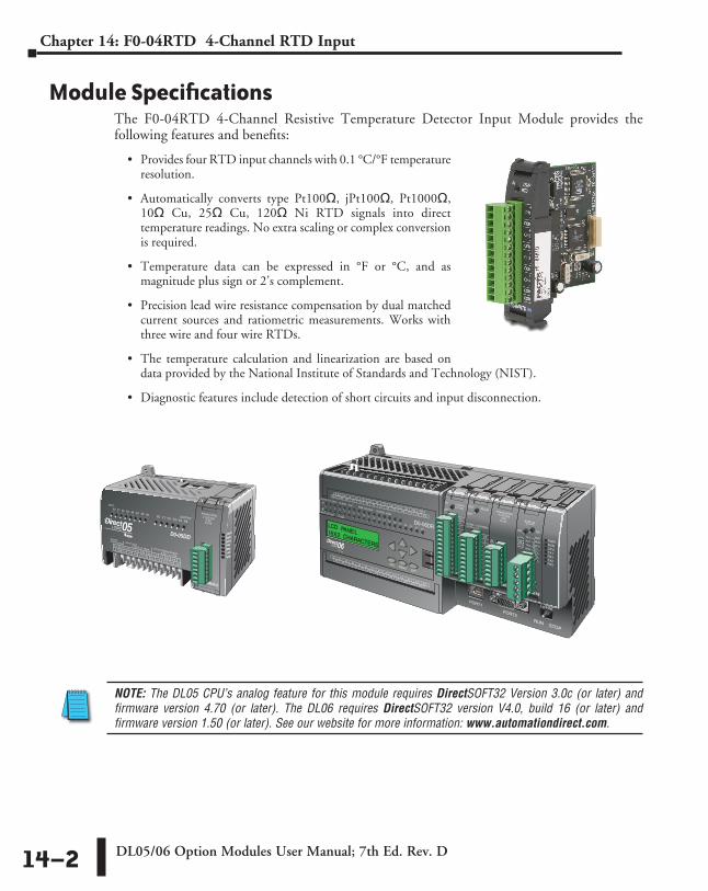
DL05/06 Option Modules User Manual; 7th Ed. Rev. D14–2
Chapter 14: F0-04RTD 4-Channel RTD Input
Module SpecificationsThe F0-04RTD 4-Channel Resistive Temperature Detector Input Module provides the following features and benefits:
• Provides four RTD input channels with 0.1 °C/°F temperature resolution.
• Automatically converts type Pt100q, jPt100q, Pt1000q, 10q Cu, 25q Cu, 120q Ni RTD signals into direct temperature readings. No extra scaling or complex conversion is required.
• Temperature data can be expressed in °F or °C, and as magnitude plus sign or 2’s complement.
• Precision lead wire resistance compensation by dual matched current sources and ratiometric measurements. Works with three wire and four wire RTDs.
• The temperature calculation and linearization are based on data provided by the National Institute of Standards and Technology (NIST).
• Diagnostic features include detection of short circuits and input disconnection.
NOTE: The DL05 CPU’s analog feature for this module requires DirectSOFT32 Version 3.0c (or later) and firmware version 4.70 (or later). The DL06 requires DirectSOFT32 version V4.0, build 16 (or later) and firmware version 1.50 (or later). See our website for more information: www.automationdirect.com.
PWR
RUN
CPU
TX1
RX1
TX2
RX2

DL05/06 Option Modules User Manual; 7th Ed. Rev. D 14–3
Chapter 14: F0-04RTD 4-Channel RTD Input
Module CalibrationThe module automatically re-calibrates every five seconds to remove any offset and gain errors. The F0-04RTD module requires no user calibration. However, if your process requires calibration, it is possible to correct the RTD tolerance using ladder logic. You can subtract or add a constant to the actual reading for that particular RTD. The actual reading can also be scaled to obtain the desired value using ladder logic.
Input SpecificationsThe following table provide the specifications for the F0-04RTD Input Module. Review these specifications to make sure the module meets your application requirements.
Input SpecificationsNumber of Channels 4Input Ranges Pt100: -200.0 °C to 850.0 °C (-328°F to 1562°F)
PT1000: -200.0 °C to 595.0 °C (-328°F to 1103°F)jPt100: -38.0 °C to 450.0 °C (-36°F to 842°F)10q Cu: -200.0 °C to 260.0 °C (-328°F to 500°F)25q Cu: -200.0 °C to 260.0 °C (-328°F to 500°F)120q Ni: -80.0 °C to 260.0 °C (-112°F to 500°F)
Resolution 16 bit (1 in 65535)Display Resolution ±0.1 °C, ±0.1 °F (±3276.7)Absolute Maximum Ratings Fault Protected Inputs to ±50VDCConverter Type Charge Balancing, 24 bitSampling Rate 140ms per channelLinearity Error (End to End) ±0.05 °C maximum, ±0.01 °C typicalPLC Update Rate 4 channels/scanTemperature Drift 15ppm / °C maximumMaximum Inaccuracy ±1 °CRTD Excitation Current 200µACommon Mode Range 0–5 VDCNotch Filter (Common Mode Rejection) >50db notches at 50/60HzDigital Input Points Required None; uses special V-memory locations based on slotPower Budget Requirements 70mA @ 5VDC (supplied by base)Operating Temperature 0 to 60° C (32 to 140° F)Storage Temperature -20 to 70° C (-4 to 158° F)Relative Humidity 5 to 95% (non-condensing)Environmental Air No corrosive gases permittedVibration MIL STD 810C 514.2Shock MIL STD 810C 516.2Noise Immunity NEMA ICS3-304Replacement Terminal Block D0-ACC-4
Wire Size Range & Connector Screw Torque 28–16 AWG; 3.5 inch-pounds (0.4 N·m); TW-SD-VSL-1 screwdriver recommended

DL05/06 Option Modules User Manual; 7th Ed. Rev. D14–4
Chapter 14: F0-04RTD 4-Channel RTD Input
Connecting and Disconnecting the Field WiringWiring Guidelines
Your company may have guidelines for wiring and cable installation. If so, you should check those before you begin the installation. Here are some general things to consider:
• Use the shortest wiring route whenever possible.
• Use shielded wiring and ground the shield at the transmitter source. Do not ground the shield at both the module and the source.
• Unused channels require shorting wires (jumpers) installed from terminals CH+ to CH– to COM.
• Do not run the signal wiring next to large motors, high current switches, or transformers. This may cause noise problems.
• Route the wiring through an approved cable housing to minimize the risk of accidental damage. Check local and national codes to choose the correct method for your application.
To remove the terminal block, disconnect power to the PLC and the field devices. Pull the terminal block firmly until the connector separates from the module.
You can remove the RTD module from the PLC by folding out the retaining tabs at the top and bottom of the module. As the retaining tabs pivot upward and outward, the module’s connector is lifted out of the PLC socket. Once the connector is free, you can lift the module out of its slot.
Use the following diagram to connect the field wiring. If necessary, the F0–04RTD terminal block can be removed to make removal of the module possible without disturbing field wiring.
RTD - Resistance Temperature DetectorUse shielded RTDs whenever possible to minimize noise on the input signal. Ground the shield wire at one end only, preferably at the RTD source.
Lead Configuration for RTD SensorsThe suggested three-lead configuration shown below provides one lead to the CH+ terminal, one lead to the CH– terminal, and one lead to the common terminal. Compensation circuitry nulls out the lead length for accurate temperature measurements.
Some sensors have four leads. When making connections, do not connect the second lead to the CH+ input; leave that lead unconnected.
Do not use configurations that lack the use of the same color lead to both the CH– and COM terminals. There is no compensation and temperature readings will be inaccurate.
This module has low RTD excitation current, worst-case dissipation with 100q RTDs connected is only 0.016mW.
RedRed
WhiteWhite
(if applicable)
To CH–
To CH+
Wiring Connections For Typical RTD Sensor
Sensor
(if sensor has 4 leads, onlyconnect one lead to CH+)
No Connection
To COM

DL05/06 Option Modules User Manual; 7th Ed. Rev. D 14–5
Chapter 14: F0-04RTD 4-Channel RTD Input
Ambient Variations in TemperatureThe F0-04RTD module has been designed to operate within the ambient temperature range of 0°C to 60°C.
Precision analog measurement with no long term temperature drift is assured by a chopper stabilized programmable gain amplifier, ratiometric referencing, and automatic offset and gain calibration.
Wiring DiagramUse the following diagram to connect the field wiring. If necessary, the F0-04RTD terminal block can be removed to make removal of the module possible without disturbing field wiring.
A/D+-
200 ACurrentSource
200 ACurrentSource
Ref.Adj.
AN
ALO
GM
ULTIP
LEX
ERxNote 3
Note 1
COM
COM
COM
COMCOM
CH1+CH1-
CH2+CH2-
CH3+CH3-
CH4+CH4-
Note 2 COM
COM
COM
COMCOM
RTD
F0-04RTD
Notes:
1. The three wires connecting the RTD to the module must be the same type and length. Do not use the shield or drain wire for the third connection.
2. Unused channels require shorting wires (jumpers) installed from terminals CH+ to CH– to COM to prevent possible noise from influencing active channels. This should be done even if the unused channel is not enabled in the V-memory configuration.
3. If a RTD sensor has four wires, the plus sense wire should be left unconnected as shown.

DL05/06 Option Modules User Manual; 7th Ed. Rev. D14–6
Chapter 14: F0-04RTD 4-Channel RTD Input
Module OperationChannel Scanning Sequence
The DL05 and DL06 read all four input channels data during each scan. The CPUs support special V-memory locations that are used to manage the data transfer. This is discussed in more detail on the following page, “Special V-memory Locations”.
Analog Module UpdateEven though the channel updates to the CPU are synchronous with the CPU scan, the module asynchronously monitors the analog transmitter signal and converts the signal to a 16-bit binary representation. This enables the module to continuously provide accurate measurements without slowing down the discrete control logic in the RLL program.
The time required to sense the temperature and copy the value to V-memory is 140 milliseconds minimum to 560 milliseconds plus 1 scan time maximum (number of channels x 140 milliseconds + 1 scan time).
Read the data
Store data
Read Inputs
Execute Application Program
Scan
Write to Outputs
Ch 1, 2, 3, 4Scan N
Scan N+1
Scan N+2
Scan N+3
Scan N+4
Ch 1, 2, 3, 4
Ch 1, 2, 3, 4
Ch 1, 2, 3, 4
Ch 1, 2, 3, 4
DL05/DL06 PLC

DL05/06 Option Modules User Manual; 7th Ed. Rev. D 14–7
Chapter 14: F0-04RTD 4-Channel RTD Input
Special V-memory LocationsThe DL05 and DL06 PLCs have special V-memory locations assigned to their respective option slots. These V-memory locations allow you to:
• Specify the number of input channels enabled and BCD/Binary data format
• Specify the input pointer address
• Specify the RTD input type
• Specify the units code – temperature scale and data format
• Specify burnout data value at burnout
• Read module setup diagnostics
Module Configuration Registers
The table below shows the special V-memory locations used by the DL05 and DL06 PLCs for the F0–04RTD module.
A: Number of Channels Enabled/Data Format Register
This V-memory location is used to define the number of input channels to be enabled and to set the channel data to BCD or binary format.
Module Configuration Parameters
DL05 and DL06 Option SlotDL05 Slot
DL06 Slot 1
DL06 Slot 2
DL06 Slot 3
DL06 Slot 4
A: Number of Channels Enabled / Data Format V7700 V700 V710 V720 V730
B: Input Pointer V7701 V701 V711 V721 V731C: RTD Type V7703 V703 V713 V723 V733D: Units Code V7704 V704 V714 V724 V734
E: RTD Burnout Data Value V7706 V706 V716 V726 V736
F: Diagnostic Error V7707 V707 V717 V727 V737
Number of Channels Enabled
Channel Data in BCD Format
Channel Data in Binary Format
1 Channel K100 K81002 Channels K200 K82003 Channels K300 K83004 Channels K400 K8400
MSB LSB
Data Format
Number of channels

DL05/06 Option Modules User Manual; 7th Ed. Rev. D14–8
Chapter 14: F0-04RTD 4-Channel RTD Input
B: Input Pointer RegisterThis is a system parameter that points to a V-memory location used for storing module channel input data. The V-memory location loaded in the input pointer V-memory location is an octal number identifying the first V-memory location for the input data. This V-memory location is user defined, but must use available consecutive V-memory locations. For example, loading O2000 causes the pointer to write Ch 1’s data value to V2000/2001, Ch 2’s data value to V2002/2003, CH 3’s data value to V2004/2005 and Ch 4’s data value to V2006/2007.
NOTE: Each channel’s data value occupies two (2) consecutive V-memory locations. This allows for more than four (4) digits to be displayed if a BCD format for channel data is selected. For example: 1234.5 °F. A binary format for either a 15-bit magnitude plus sign or 16-bit 2’s complement value will occupy the first V-memory location of the two V-memory locations assigned for the selected channel. Refer to the specific PLC’s user manual being used for available user V-memory locations.
C: RTD Type Selection RegisterThe F0-04RTD module supports six different RTD types. The type must be specified by placing a value from the table shown below into a V-memory register. The register is determined by the PLC type and slot number, as listed in the Module Configuration Registers table on the previous page. For example, if using a Pt1000 RTD with a module installed in slot 2 of a DL06, load a value of 4 into V713. All channels of the module must be the same RTD type.
The factory default setting is for Pt100q RTDs. This selects the DIN 43760 European platinum type RTD. European curve type RTDs are calibrated to DIN 43760, BS1905, or IEC751 specifications which is 0.00385 q/q/°C (100 °C = 138.5 q).
The jPt100 type for the American curve 100q platinum RTD is more commonly used in North America.
The Cu10 (10q) and Cu25 (25q) RTD settings are used with copper RTDs.
RTD Type
Input Selection
Pt100 (European curve w/TCR = 0.00385) K0Cu10 K1Cu25 K2jPt100 (American curve w/TCR = 0.00392) K3Pt1000 K4Ni120 K5
MSB LSB
Input Type
Selection
V-memory register

DL05/06 Option Modules User Manual; 7th Ed. Rev. D 14–9
Chapter 14: F0-04RTD 4-Channel RTD Input
D: Units Code RegisterAll RTD types are converted into a direct temperature reading in either Fahrenheit or Celsius. The data contains one implied decimal place. For example, a value in V-memory of 1002 would be 100.2 °C or °F.
All RTD ranges can include negative temperatures, therefore the display resolution is from –3276.7 to +3276.7.
Negative temperatures can be represented in either 2’s complement or magnitude plus sign form. If the temperature is negative, the most significant bit in the V-memory location is set.
The 2’s complement data format may be required to correctly display bipolar data on some operator interfaces. This data format could also be used to simplify averaging a bipolar signal. To view this data format in DirectSoft32, select Signed Decimal.
The bipolar input ranges may be converted to a 15-bit magnitude plus sign or a 16-bit 2’s complement value.
Bit 0 = Temperature Scale 0 = Temp in degrees F 1 = Temp in degrees C
Bit 1 = Data Format 0 = Magnitude plus sign bit format 1 = 2’s Complement format
MSB LSB
Temp scale
Data Format
Unit Code Register - Truth TableTemperature Scale Data Format Bit 1 Bit 0 Value
°F Magnitude + sign bit 0 0 K0
°C Magnitude + sign bit 0 1 K1
°F 2’s Complement 1 0 K2
°C 2’s Complement 1 1 K3

DL05/06 Option Modules User Manual; 7th Ed. Rev. D14–10
Chapter 14: F0-04RTD 4-Channel RTD Input
E: RTD Burnout Data Value RegisterThis register is used to define either up scale or down scale channel values when a channel RTD burnout occurs.
Bit 0 = Up scale/down scale value at Burnout 0 = Up scale value at Burnout, 7FFFh (BCD/HEX) or 32767 (Binary) written to CH register 1 = Down scale value at Burnout: 0000h (BCD/HEX) or 0 (Binary) written to CH register
F: Diagnostics Error RegisterThis register is used to determine whether the configuration of the module is valid or not.
Bit 0 = Diagnostic bit: 0 = Module setup is valid 1 = Module setup is not valid
MSB LSB
Up scale/down scale Burnout value
MSB LSB
Diagnostics bit

DL05/06 Option Modules User Manual; 7th Ed. Rev. D 14–11
Chapter 14: F0-04RTD 4-Channel RTD Input
Configuring the Module in Your Control ProgramDL05 Example 1
The example program below shows how to setup the F0–04RTD for 4 input channels enabled, use of a type Pt100 RTD on all 4 input channels, BCD channel data format, the Fahrenheit (°F ) temperature scale, magnitude plus sign bit format, and an up scale burnout value specified. Place this rung anywhere in the ladder program or in the initial stage if you are using stage programming instructions.
This is all that is required to read the temperature or voltage input data into V-memory locations. Once the data is in V-memory you can perform mathematical calculations with the data, compare the data against preset values, etc. V2000 is used in the example but you can use any user V-memory location.
LDSP0
LD
LDAO2000
OUTV7701
This loads an octal value for the first V-memory location that will be usedto store the incoming data. For example, the O2000 entered here usingthe LDA instruction would designate the following addresses:Ch1 – V2000/2001, Ch2 – V2002/2003, Ch3 – V2004/2005,
The octal address (O2000) is stored here. Special V–memory locationV7701 is assigned to the option slot and acts as a pointer, whichmeans the CPU will use the octal value in this location to determineexactly where to store the incoming data.
Special V-memory location assigned to the option slot that specifiesthe data format and the number of channels to scan.
Loads a constant that specifies the number of input channels to scanand the data format. The upper byte, most significant nibble (MSN)selects the data format (0 = BCD, 8 = binary). The LSN selects thenumber of channels (1, 2, 3 or 4).
- or -
The binary format is used for displaying data on some operator interface units. K8400 enables 4 channels in binary format.
LDK0
Loads a 0 into the accumulator to set the following parameters in (V7703 – V7706).
Special V–memory location assigned to the option slot that specifiesthe RTD Input Type. K0 selects a type Pt100 RTD.
K0400 K8400
OUTV7704
OUTV7700
OUTV7703
Special V–memory location assigned to the option slot that specifiesthe Units Code (temperature scale and data format) selections.K0 selects a º F temperature scale and magnitude plus sign bit format.
OUTV7706
Special V–memory location assigned to the option slot that specifiesthe RTD up scale/down scale burnout value. K0 selects an upscale burnout value of 7FFFh (BCD/HEX) or 32,767 (Binary). The valueis written to the channel input register when a RTD burnout occurs.
See table on page 14-8 for selections.
See truth table on page 14-9 for selections.
Ch4 – V2006/2007. See note on page 14-8.

DL05/06 Option Modules User Manual; 7th Ed. Rev. D14–12
Chapter 14: F0-04RTD 4-Channel RTD Input
DL05 Example 2The example program below shows how to setup the F0–04RTD for 2 input channels enabled, use of a type Cu10 RTD on the first 2 input channels, BCD channel data format, Celsius (ºC) temperature scale, 2’s complement format, and with a down-scale burnout value specified. Again, place this rung in the ladder program or in the initial stage if you are using stage programming instructions.
LDSP0
LD
LDAO2000
OUTV7701
This loads an octal value for the first V-memory location that will be usedto store the incoming data. For example, the O2000 entered here usingthe LDA instruction would designate the following addresses:Ch1 – V2000/2001, Ch2 – V2002/2003
The octal address (O2000) is stored here. Special V–memory locationV7701 is assigned to the option slot and acts as a pointer, whichmeans the CPU will use the octal value in this location to determineexactly where to store the incoming data.
Special V-memory location assigned to the option slot that specifiesthe data format and the number of channels to scan.
Loads a constant that specifies the number of input channels to scanand the data format. The upper byte, most significant nibble (MSN)selects the data format (0 = BCD, 8 = binary). The LSN selects thenumber of channels (1, 2, 3 or 4).
- or -
The binary format is used for displaying data on some operatorinterface units. K8200 enables 2 channels in binary format.
LDK1
LDK3
Loads a constant that specifies the RTD input type. K1 selects a typeCu10 RTD. Enter a K0–K5 to specify the RTD Input Type.
Special V–memory location assigned to the option slot that specifiesthe RTD input type.
K0200 K8200
OUTV7704
OUTV7700
OUTV7703
Loads a constant that specifies the Units Code (temperature scale anddata format). K3 selects º C and 2’s complement data format. See truth table on page 14-9 for selections.
Special V–memory location assigned to the option slot that specifiesthe temperature scale and data format selections.
LDK1
OUTV7706
Loads a constant that specifies the RTD burnout data value at burnout.K1 specifies a down scale value of 0000h (BCD/HEX) or 0 (Binary) to
Special V–memory location assigned to the option slot that specifiesthe RTD up scale/down scale burnout value. The value is writtento the channel input register when a RTD burnout occurs.
See table on page 14-8 for selections.
be written to the channel input register when a RTD burnout occurs.
See note on page 14-8.
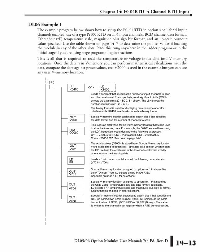
DL05/06 Option Modules User Manual; 7th Ed. Rev. D 14–13
Chapter 14: F0-04RTD 4-Channel RTD Input
DL06 Example 1The example program below shows how to setup the F0–04RTD in option slot 1 for 4 input channels enabled, use of a type Pt100 RTD on all 4 input channels, BCD channel data format, Fahrenheit (ºF) temperature scale, magnitude plus sign bit format, and an up-scale burnout value specified. Use the table shown on page 14–7 to determine the pointer values if locating the module in any of the other slots. Place this rung anywhere in the ladder program or in the initial stage if you are using stage programming instructions.
This is all that is required to read the temperature or voltage input data into V-memory locations. Once the data is in V-memory you can perform mathematical calculations with the data, compare the data against preset values, etc. V2000 is used in the example but you can use any user V-memory location.
LDSP0
LD
LDAO2000
OUTV701
This loads an octal value for the first V-memory location that will be usedto store the incoming data. For example, the O2000 entered here usingthe LDA instruction would designate the following addresses:Ch1 – V2000/2001, Ch2 – V2002/2003, Ch3 – V2004/2005,
The octal address (O2000) is stored here. Special V–memory locationV701 is assigned to option slot 1 and acts as a pointer, which meansthe CPU will use the octal value in this location to determine exactlywhere to store the incoming data.
Special V-memory location assigned to option slot 1 that specifiesthe data format and the number of channels to scan.
Loads a constant that specifies the number of input channels to scanand the data format. The upper byte, most significant nibble (MSN)selects the data format (0 = BCD, 8 = binary). The LSN selects thenumber of channels (1, 2, 3 or 4).
- or -
The binary format is used for displaying data on some operator interface units. K8400 enables 4 channels in binary format.
LDK0
Loads a 0 into the accumulator to set the following parameters in (V703 – V706).
Special V–memory location assigned to option slot 1 that specifiesthe RTD Input Type. K0 selects a type Pt100 RTD.
K0400 K8400
OUTV704
OUTV700
OUTV703
Special V–memory location assigned to option slot 1 that specifiesthe Units Code (temperature scale and data format) selections.K0 selects a º F temperature scale and magnitude plus sign bit format.
OUTV706
Special V–memory location assigned to option slot 1 that specifies theRTD up scale/down scale burnout value. K0 selects an up scaleburnout value of 7FFFh (BCD/HEX) or 32,767 (Binary). The valueis written to the channel input register when a RTD burnout occurs.
See table on page 14-8 for selections.
See truth table on page 14-9 for selections.
Ch4 – V2006/2007. See note on page 14-8.

DL05/06 Option Modules User Manual; 7th Ed. Rev. D14–14
Chapter 14: F0-04RTD 4-Channel RTD Input
DL06 Example 2The example program below shows how to setup the F0–04RTD in option slot 2 for 2 input channels enabled, use of a type Cu10 RTD on the first 2 input channels, BCD channel data format, Celsius (ºC ) temperature scale, 2’s complement format, and with a down scale burnout value specified. Use the table shown on page 14–7 to determine the pointer values if locating the module in any of the other slots. V-memory location V3000 is shown in the example, but you can use any available user V-memory location. Again, place this rung anywhere in the ladder program or in the initial stage if you are using stage programming instructions.
LDSP0
LD
LDAO3000
OUTV711
This loads an octal value for the first V-memory location that will be usedto store the incoming data. For example, the O3000 entered here usingthe LDA instruction would designate the following addresses:Ch1 – V3000/3001, Ch2 – V3002/3003
The octal address (O3000) is stored here. Special V–memory locationV711 is assigned to option slot 2 and acts as a pointer, whichmeans the CPU will use the octal value in this location to determineexactly where to store the incoming data.
Special V-memory location assigned to option slot 2 that specifiesthe data format and the number of channels to scan.
Loads a constant that specifies the number of input channels to scanand the data format. The upper byte, most significant nibble (MSN)selects the data format (0 = BCD, 8 = binary). The LSN selects thenumber of channels (1, 2, 3 or 4).
- or -
The binary format is used for displaying data on some operatorinterface units. K8200 enables 2 channels in binary format.
LDK1
LDK3
Loads a constant that specifies the RTD input type. K1 selects a typeCu10 RTD. Enter a K0–K5 to specify the RTD Input Type.
Special V–memory location assigned to option slot 2 that specifiesthe RTD input type.
K0200 K8200
OUTV714
OUTV710
OUTV713
Loads a constant that specifies the Units Code (temperature scale anddata format). K3 selects º C and 2’s complement data format. See truth table on page 14-9 for selections.
Special V–memory location assigned to option slot 2 that specifiesthe temperature scale and data format selections.
LDK1
OUTV716
Loads a constant that specifies the RTD burnout data value at burnout.K1 specifies a down scale value of 0000h (BCD/HEX) or 0 (Binary) to
Special V–memory location assigned to option slot 2 that specifiesthe RTD up scale/down scale burnout value. The value is writtento the channel input register when a RTD burnout occurs.
be written to the channel input register when a RTD burnout occurs.
See table on page 14-8 for selections.
See note on page 14-8.

DL05/06 Option Modules User Manual; 7th Ed. Rev. D 14–15
Chapter 14: F0-04RTD 4-Channel RTD Input
Negative Temperature Readings with Magnitude Plus SignWith bipolar ranges, you need some additional logic to determine whether the value being returned represents a positive temperature or a negative temperature. There is a simple solution:
• If you are using bipolar ranges and you get a value greater than or equal to 8000h, the value is negative.
• If you get a value less than or equal to 7FFFh, the value is positive.
The sign bit is the most significant bit, which combines 8000h to the data value. If the value is greater than or equal to 8000h, you only have to mask the most significant bit and the active channel bits to determine the actual data value.
The following two programs show how you can accomplish this. The first example uses magnitude plus sign (binary) and the second example uses magnitude plus sign (BCD).
Since you always want to know when a value is negative, these rungs should be placed before any other operations that use the data, such as math instructions, scaling operations, and so forth. Also, if you are using stage programming instructions, these rungs should be in a stage that is always active. Note: you only need this logic for each channel that is using bipolar input signals. The examples only show two channels.
Magnitude Plus Sign (Binary)
SP1
OUT
C1
LDV2000
OUTV2010
Load channel 1 data from V-memory into theaccumulator. Contact SP1 is always on.
Put the actual signal value in V2010. Now you can usethe data normally.
ANDK7FFF
This instruction masks the sign bit of the binary data, ifit is set. Without this step, negative values will not becorrect so do not forget to include it.
V2000 K8000Channel 1 data is negative when C1 is on (a value of–1.0 reads as 8010, –2.0 is 8020, etc.).
SP1
OUT
C2
LDV2002
OUTV2012
Load channel 2 from V-memory into the accumulator.Contact SP1 is always on.
Put the actual signal value in V2012. Now you can usethe data normally.
ANDK7FFF
This instruction masks the sign bit of the binary data, ifit is set. Without this step, negative values will not becorrect so do not forget to include it.
V2002 K8000Channel 2 data is negative when C2 is on (a value of–1.0 reads as 8010, –2.0 is 8020, etc.).
M
M
Check Channel 1
Check Channel 2

DL05/06 Option Modules User Manual; 7th Ed. Rev. D14–16
Chapter 14: F0-04RTD 4-Channel RTD Input
Magnitude Plus Sign (BCD)
SP1
OUT
C1
LDDV2000
OUTDV2010
Load channel 1 data from V-memory into theaccumulator. Remember, the data can be negative.Contact SP1 is always on.
Put the actual signal value in V2010. Now you can usethe data normally.
ANDDK7FFFFFFF
This instruction masks the sign bit of the BCD data, if itis set. Without this step, negative values will not becorrect so do not forget to include it.
V2001 K8000
Check Channel 1
Check Channel 2
Channel 1 data is negative when C1 is on (a value of–1.0 reads as 8000 0010, –2.0 is 8000 0020, etc.).
SP1
OUT
C2
LDDV2002
OUTDV2012
Load channel 2 from V-memory into the accumulator.Remember, the data can be negative. Contact SP1 isalways on.
Put the actual signal value in V2012. Now you can usethe data normally.
ANDDK7FFFFFFF
This instruction masks the sign bit of the BCD data, if itis set. Without this step, negative values will not becorrect so do not forget to include it.
V2003 K8000Channel 2 data is negative when C2 is on (a value of–1.0 reads as 8000 0010, –2.0 is 8000 0020, etc.).
M
M

DL05/06 Option Modules User Manual; 7th Ed. Rev. D 14–17
Chapter 14: F0-04RTD 4-Channel RTD Input
Negative Temperatures 2’s Complement (Binary/Pointer Method)You can use the 2’s complement mode for negative temperature display purposes, while at the same time using the magnitude plus sign of the temperature in your control program. The DirectSOFT32 element Signed Decimal is used to display negative numbers in 2’s complement form. To find the absolute value of a negative number in 2’s complement, invert the number and add 1 as shown in the following example:
LDV2000
ADDDK1
Load negative value into the accumulator so we can convert it to a positive value.
Add 1.
INVInvert the binary pattern in the accumulator.
V2000 K8000
M
OUTV2010
Save Channel 1 data at V2010.
Repeat for other channels as required.

DL05/06 Option Modules User Manual; 7th Ed. Rev. D14–18
Chapter 14: F0-04RTD 4-Channel RTD Input
Analog Input Ladder Logic FilterPID Loops / Filtering
Please refer to the “PID Loop Operation” chapter in the DL06 or DL05 User Manual for information on the built-in PV filter (DL05/06) and the ladder logic filter (DL06 only) shown below. A filter must be used to smooth the analog input value when auto tuning PID loops to prevent giving a false indication of loop characteristics.
Smoothing the Input Signal (DL06 only)The filter logic can also be used in the same way to smooth the analog input signal to help stabilize PID loop operation or to stabilize the analog input signal value for use with an operator interface display, etc.
WARNING: The built-in and logic filters are not intended to smooth or filter noise generated by improper field device wiring or grounding. Small amounts of electrical noise can cause the input signal to bounce considerably. Proper field device wiring and grounding must be done before attempting to use the filters to smooth the analog input signal.
Using Binary Data Format
LDV2000
SUBRV1400
BTOR
SP1Loads the analog signal, which is in binary formatand has been loaded from V-memory locationV2000, into the accumulator. Contact SP1 isalways on.
Converts the binary value in the accumulatorto a real number.
Subtracts the real number stored in locationV1400 from the real number in the accumulator,and stores the result in the accumulator. V1400is the designated workspace in this example.
Multiplies the real number in the accumulator by0.2 (the filter factor), and stores the result in theaccumulator. This is the filtered value. The filterrange is 0.1 to 0.9. Smaller filter factorsincreases filtering. (1.0 eliminates filtering).
OUTDV1400
ADDRV1400
MULRR0.2
OUTV1402
RTOB
Adds the real number stored inlocation V1400 to the real numberfiltered value in the accumulator, andstores the result in the accumulator.
Copies the value in the accumulator tolocation V1400.
Converts the real number in theaccumulator to a binary value, andstores the result in the accumulator.
Loads the binary number filtered value fromthe accumulator into location V1402 to use inyour application or PID loop.

DL05/06 Option Modules User Manual; 7th Ed. Rev. D 14–19
Chapter 14: F0-04RTD 4-Channel RTD Input
NOTE: Be careful not to do a multiple number conversion on a value. For example, if you are using the pointer method in BCD format to get the analog value, it must be converted to binary (BIN) as shown below. If you are using the pointer method in Binary format, the conversion to binary (BIN) instruction is not needed.
Using BCD Data Format
LDDV2000
SUBRV1400
BTOR
SP1
BIN
Loads the analog signal, which is in BCD formatand has been loaded from V-memory locationV2000, into the accumulator. Contact SP1 isalways on.
Converts a BCD value in the accumulator tobinary.
Converts the binary value in the accumulatorto a real number.
Subtracts the real number stored in locationV1400 from the real number in the accumulator,and stores the result in the accumulator. V1400is the designated workspace in this example.
Multiplies the real number in the accumulator by0.2 (the filter factor), and stores the result in theaccumulator. This is the filtered value. The filterrange is 0.1 to 0.9. Smaller filter factorsincreases filtering. (1.0 eliminates filtering).
OUTDV1400
ADDRV1400
MULRR0.2
OUTDV1402
BCD
RTOB
Adds the real number stored inlocation V1400 to the real numberfiltered value in the accumulator, andstores the result in the accumulator.
Copies the value in the accumulator tolocation V1400.
Converts the real number in theaccumulator to a binary value, andstores the result in the accumulator.
Converts the binary value in the accumulatorto a BCD number. Note: The BCD instructionis not needed for PID loop PV (loop PV is abinary number).
Loads the BCD number filtered value fromthe accumulator into location V1402 to use inyour application or PID loop.

DL05/06 Option Modules User Manual; 7th Ed. Rev. D14–20
Chapter 14: F0-04RTD 4-Channel RTD Input
RTD Burnout Detection BitsSpecial Relays Corresponding to RTD Burnouts
The following Special Relay (SP) bits can be used in your program to monitor for RTD burnout.
SP bit : 0 = RTD OK 1 = RTD burnout
Module ChannelDL05 and DL06 Option Slot
DL05 Slot
DL06 Slot 1
DL06 Slot 2
DL06 Slot 3
DL06 Slot 4
Channel 1 SP600 SP140 SP240 SP340 SP440
Channel 2 SP601 SP141 SP241 SP341 SP441
Channel 3 SP602 SP142 SP242 SP342 SP442
Channel 4 SP603 SP143 SP243 SP343 SP443

151515F0-04THM 4-CHannel THerMoCouple InpuT
ChapterChapterChapter
In This Chapter...Module Specifications .............................................................................................15–2
Connecting and Disconnecting the Field Wiring ...................................................15–4
Module Operation ...................................................................................................15–7
Special V-memory Locations ...................................................................................15–8
Configuring the Module in Your Control Program ..............................................15–12
Negative Temperature Readings with Magnitude Plus Sign ...............................15–16
Module Resolution .................................................................................................15–18
Analog Input Ladder Logic Filter ..........................................................................15–19
Thermocouple Burnout Detection Bits .................................................................15–21

DL05/06 Option Modules User Manual; 7th Ed. Rev. D15–2
Chapter 15: F0-04THM 4-Channel Thermocouple Input
Module SpecificationsThe F0-04THM 4-Channel Thermocouple Input Module provides the following features and benefits:
• Four thermocouple input channels with 16-bit voltage resolution or 0.1 °C/°F temperature resolution.
• Automatically converts type E, J, K, R, S, T, B, N, or C thermocouple signals into direct temperature readings. No extra scaling or complex conversion is required.
• Temperature data can be expressed in °F or °C.
• Module can be configured as 0–39.0625 mVDC, ±39.0625 mVDC, ±78.125 mVDC, 0–156.25 mV, ±156.25 mVDC and 0–1.25 VDC input and will convert volts and millivolt signal levels into 16-bit digital (0–65535) values.
• Signal processing features include automatic cold junction compensation (CJC), thermocouple linearization, and digital filtering.
• The temperature calculation and linearization are based on data provided by the National Institute of Standards and Technology (NIST).
• Diagnostic features include detection of thermocouple burnout or disconnection.
NOTE: The DL05 CPU’s analog feature for this module requires DirectSOFT32 Version 3.0c (or later) and firmware version 4.60 (or later). The DL06 requires DirectSOFT32 version V4.0, build 16 (or later) and firmware version 1.40 (or later). See our website for more information: www.automationdirect.com.
PWR
RUN
CPU
TX1
RX1
TX2
RX2

DL05/06 Option Modules User Manual; 7th Ed. Rev. D 15–3
Chapter 15: F0-04THM 4-Channel Thermocouple Input
The following tables provide the specifications for the F0-04THM Analog Input Module. Review these specifications to make sure the module meets your application requirements.
General SpecificationsNumber of Channels 4, differential inputs, voltage or thermocoupleCommon Mode Range -1.3 VDC to +3.8 VDCConversion Time 270ms / channelCommon Mode Rejection > 100dB @ 50/60Hz.Input Impedance 5Mq min.Absolute Maximum Ratings Fault-protected inputs to ±50VDCAccuracy vs. Temperature Max. full scale error (including offset)
±15ppm / ºC maximum (Full scale);±35ppm / ºC maximum (0–1.25 V)
PLC Update Rate 4 channels per scanPower Budget Requirement 30mA @ 5VDC (supplied by base)Operating Temperature 0 to 60ºC (32 to 140ºF)Storage Temperature -20 to 70ºC (-4 to 158ºF)Relative Humidity 5 to 95% (non-condensing)Environmental Air No corrosive gases permittedVibration MIL STD 810C 514.2Shock MIL STD 810C 516.2Noise Immunity NEMA ICS3-304Replacement Terminal Block F0-IOCON-THM (comes with CJC)
Wire Size Range & Connector Screw Torque 22–16 AWG; 1.7 inch-pounds (0.192 N·m); TW-SD-VSL-1 Screwdriver Recommended
Thermocouple SpecificationsInput Ranges Type J -190 to 760 ºC (-310 to 1400 ºF)
Type K -150 to 1372 ºC (-238 to 2502 ºF) Type E -210 to 1000 ºC (-346 to 1832 ºF) Type R 65 to 1768 ºC (149 to 3214 ºF) Type S 65 to 1768 ºC (149 to 3214 ºF) Type T -230 to 400 ºC (-382 to 752 ºF) Type B 529 to 1820 ºC (984 to 3308 ºF) Type N -70 to 1300 ºC (-94 to 2372 ºF) Type C 65 to 2320 ºC (149 to 4208 ºF)
Display Resolution ±0.1 ºC or ±0.1 ºFCold Junction Compensation AutomaticWarm-Up Time 30 minutes typically ± 1ºC repeatabilityLinearity Error (End to End) ±1ºC maximum, ±0.5 ºC typicalMaximum Inaccuracy ±3ºC (excluding thermocouple error)
Voltage Input SpecificationsVoltage Ranges 0-39.0625 mVDC, ±39.0625 mVDC, ±78.125 mVDC,
0-156.25 mVDC, ±156.25 mVDC, 0-1.25 VDCResolution 16 bit (1 in 65535)Max. Offset Error (All Input Ranges) 0.05% @ 0-60 ºC; Typical: 0.04% @ 25 ºCLinearity Error (All Input Ranges) 0.05% @ 0-60 ºC; Typical: 0.03% @ 25 ºCMaximum Inaccuracy 0-39.0625 mVDC, ±39.0625 mVDC, ±78.125 mVDC ranges:
0.1% @ 0-60ºC; Typical: 0.04% @ 25ºC0-156.25 mVDC, ±156.25 mVDC, 0-1.25 VDC ranges: 0.05% @ 0-60ºC; Typical: 0.04% @ 25ºC
All percentages are calculated as a percent of 216 (65536) counts. (0.025% max error => 0.025 * 65536/100 = 16 counts max error)

DL05/06 Option Modules User Manual; 7th Ed. Rev. D15–4
Chapter 15: F0-04THM 4-Channel Thermocouple Input
Connecting and Disconnecting the Field WiringWiring Guidelines
Your company may have guidelines for wiring and cable installation. If so, you should check those before you begin the installation. Here are some general things to consider:
• Use the shortest wiring route whenever possible.
• Use shielded wiring and ground the shield at the PLC power source. Do not ground the shield at both the transmitter and the PLC power source.
• Use thermocouple extension wire that is the same as the thermocouple type when extending the length.
• Do not run the signal wiring next to large motors, high current switches, or transformers. This may cause noise problems.
• Route the wiring through an approved cable housing to minimize the risk of accidental damage. Check local and national codes to choose the correct method for your application.
To remove the terminal block, disconnect power to the PLC and the field devices. Pull the terminal block firmly until the connector separates from the module.
You can remove the thermocouple module from the PLC by folding out the retaining tabs at the top and bottom of the module. As the retaining tabs pivot upward and outward, the module’s connector is lifted out of the PLC socket. Once the connector is free, you can lift the module out of its slot.
Use the following diagram to connect the field wiring. If necessary, the F0–04THM terminal block can be removed to make removal of the module possible without disturbing field wiring.
Thermocouple Input Wiring DiagramAll of the module’s CH– terminals must be connected together. This will help eliminate ground potential differences between the input channels that could cause damage to the module. The two unlabeled terminals are internally connected and may be used for convenience to connect the CH– terminals together as shown below.
The CJC comes installed on the terminal strip
Notes: 1. Shields should be grounded at the PLC
power source only.2. Unused channels should have a shorting
wire (jumper) installed from CH+ to CH-.3. All CH- terminals must be connected
together. 4. This module is not compatible with the
ZIPLink wiring system. MU
X
CH1+
CH2+
CH3+
CH4+
CH1–
CH2–
CH3–
CH4–
LM35 CJC
CJC
CJC ADC
internalconnection
See NOTE 1
See NOTE 3
See NOTE 2
The LM35 shown in the diagram is the CJC
DL05/06 Option Modules User Manual; 7th Ed. Rev. D 15–5
Chapter 15: F0-04THM 4-Channel Thermocouple Input
ThermocouplesUse shielded thermocouples whenever possible to minimize the presence of noise on the thermocouple wire. Ground the shield wire at one end only. For both grounded and ungrounded thermocouples, connect the shield to the 0V (common) terminal of the PLC power supply.
Grounded Thermocouple AssemblyA grounded thermocouple provides better response time than an ungrounded thermocouple because the tip of the thermocouple junction is in direct contact with the protective case.
Ungrounded Thermocouple AssemblyAn ungrounded thermocouple is electrically isolated from the protective case. If the case is electrically grounded it provides a low-impedance path for electrical noise to travel. The ungrounded thermocouple provides a more stable and accurate measurement in a noisy environment. To avoid exceeding the common mode specifications, be sure that the machine assembly is properly bonded together.
Exposed Grounded ThermocoupleThe thermocouple does not have a protective case and is directly connected to a device with a higher potential. Grounding the thermocouple assures that the thermocouple remains within the common mode specifications. Because a thermocouple is essentially a wire, it provides a low-impedance path for electrical noise. The noise filter has a response of >100dB @ 50/60 Hz.
WARNING: A thermocouple can become shorted to a high voltage potential. Because common terminals are internally connected together, whatever voltage potential exists on one thermocouple will exist on the other channels.
Ambient Variations in TemperatureThe F0-04THM module has been designed to operate within the ambient temperature range of 0°C to 60°C.
The cold junction compensation is calibrated to operate in a still-air environment. If the module is used in an application that has forced convection cooling, an error of 2–3 °C may be introduced. To compensate for this you can use ladder logic to correct the values.
When configuring the system design it is best to locate any heat-producing devices above and away from the PLC chassis because the heat will affect the temperature readings. For example, heat introduced at one end of the terminal block can cause a channel-to-channel variation.
When exposing the F0-04THM module to abrupt ambient temperature changes it will take several minutes for the cold junction compensation and terminal block to stabilize. Errors introduced by abrupt ambient temperature changes will be less than 4°C.

DL05/06 Option Modules User Manual; 7th Ed. Rev. D15–6
Chapter 15: F0-04THM 4-Channel Thermocouple Input
Voltage Input Wiring DiagramAll of the module’s CH– terminals must be connected together as shown below. This will help eliminate ground potential differences between the input channels that could cause damage to the module. The two unlabeled terminals are internally connected and may be used for convenience to connect the CH– terminals together as shown below.
MU
XCH1+
CH2+
CH3+
CH4+
CH1–
CH2–
CH3–
CH4–
CJC
CJC
CJC
VoltageTransmitter
VoltageTransmitter
TransmitterSupply
+
–
2. Unused channels should have a shorting wire (jumper) installed from CH+ to CH–.3. CJC functionality is automatically disabled when a Voltage input is selected.
+
–
+
VoltageTransmitter
See NOTE 1
Notes: 1. Shields should be grounded at the PLC power source.
AD
C
internalconnection
LM35
comes
the terminalstrip.
The LM35 shownin the diagram isthe CJC
See NOTE 2
.
See NOTE 4
See NOTE 2The CJC
installed on
+
–
Self-powered

DL05/06 Option Modules User Manual; 7th Ed. Rev. D 15–7
Chapter 15: F0-04THM 4-Channel Thermocouple Input
Module OperationChannel Scanning Sequence
The DL05 and DL06 read the data from all four input channels during each scan. The CPUs support special V-memory locations that are used to manage the data transfer. This is discussed in more detail on the following page, “Special V-memory Locations”.
Analog Module UpdateEven though the channel updates to the CPU are synchronous with the CPU scan, the module asynchronously monitors the analog transmitter signal and converts the signal to a 16-bit binary representation. This enables the module to continuously provide accurate measurements without slowing down the discrete control logic in the RLL program.
The time required to sense the temperature and copy the value to V-memory is 270 milliseconds minimum to 1080 milliseconds plus 1 scan time maximum (number of channels x 270 milliseconds + 1 scan time).
Read the data
Store data
Read Inputs
Execute Application Program
Scan
Write to Outputs
Ch 1, 2, 3, 4Scan N
Scan N+1
Scan N+2
Scan N+3
Scan N+4
Ch 1, 2, 3, 4
Ch 1, 2, 3, 4
Ch 1, 2, 3, 4
Ch 1, 2, 3, 4
DL05/DL06 PLC

DL05/06 Option Modules User Manual; 7th Ed. Rev. D15–8
Chapter 15: F0-04THM 4-Channel Thermocouple Input
Special V-memory LocationsThe DL05 and DL06 PLCs have special V-memory locations assigned to their respective option slots. These V-memory locations allow you to:
• Specify the number of input channels enabled and BCD/Binary data format
• Specify the input pointer address
• Specify the thermocouple or voltage input type
• Specify the units code – temperature scale and data format
• Enable/disable thermocouple burnout detection
• Specify burnout data value at burnout
• Read module setup diagnostics
Module Configuration RegistersThe table below shows the special V-memory locations used by the DL05 and DL06 PLCs for
the F0–04THM module.
A: Number of Channels Enabled/Data Format RegisterThis V-memory location is used to define the number of input channels to be enabled and to set the channel data to BCD or binary format.
Module Configuration Parameters
DL05 and DL06 Option SlotDL05 Slot
DL06 Slot 1
DL06 Slot 2
DL06 Slot 3
DL06 Slot 4
A: Number of Channels Enabled / Data Format V7700 V700 V710 V720 V730
B: Input Pointer V7701 V701 V711 V721 V731C: Input Type V7703 V703 V713 V723 V733D: Units Code V7704 V704 V714 V724 V734E: Thermocouple Burnout Detection Enable V7705 V705 V715 V725 V735
F: Thermocouple Burnout Data Value V7706 V706 V716 V726 V736
G: Diagnostic Error V7707 V707 V717 V727 V737
Number of Channels Enabled
Channel Data in BCD Format
Channel Data in Binary Format
1 Channel K100 K81002 Channels K200 K82003 Channels K300 K83004 Channels K400 K8400
MSB LSB
Data Format
Number of channels

DL05/06 Option Modules User Manual; 7th Ed. Rev. D 15–9
Chapter 15: F0-04THM 4-Channel Thermocouple Input
B: Input Pointer RegisterThis is a system parameter that points to a V-memory location used for storing module channel input data. The V-memory location loaded in the input pointer V-memory location is an octal number identifying the first V-memory location for the input data. This V-memory location is user defined, but must use available consecutive V-memory locations. For example, loading O2000 causes the pointer to write Ch 1’s data value to V2000/2001, Ch 2’s data value to V2002/2003, CH 3’s data value to V2004/2005 and Ch 4’s data value to V2006/2007.
NOTE: Each channel’s data value occupies two (2) consecutive V-memory locations. This allows for more than four (4) digits to be displayed if a BCD format for channel data is selected. For example: 1234.5 °F. A binary format for either a 15-bit magnitude plus sign or 16-bit 2’s complement value will occupy the first V-memory location of the two V-memory locations assigned for the selected channel. Refer to the specific PLC’s user manual being used for available user V-memory locations.
C: Input Type Selection RegisterThis V-memory register must be set to match the type of thermocouple being used or the input voltage level. Use the table to determine your settings.
NOTE: The CJC functionality is automatically disabled when a Voltage input is selected.
Thermocouple/ Voltage Input Type
Input Selection
Temperature Range °C
Temperature Range °F
J K0 -190 to 760 -310 to 1400K K1 -150 to 1372 -238 to 2502E K2 -210 to 1000 -346 to 1832R K3 65 to 1768 149 to 3214S K4 65 to 1768 149 to 3214T K5 -230 to 400 -382 to 752B K6 529 to 1820 984 to 3308N K7 -70 to 1300 -94 to 2372C K8 65 to 2320 149 to 4208
0–39.0625 mVDC K9 N/A N/A±39.0625 mVDC KA N/A N/A±78.125 mVDC KB N/A N/A0-156.25 mVDC KC N/A N/A±156.25 mVDC KD N/A N/A
0–1.25 VDC KE N/A N/A
MSB LSB
Input Type
Selection

DL05/06 Option Modules User Manual; 7th Ed. Rev. D15–10
Chapter 15: F0-04THM 4-Channel Thermocouple Input
D: Units Code RegisterAll thermocouple types are converted into a direct temperature reading in either Fahrenheit or Celsius. The data contains one implied decimal place. For example, a value in V-memory of 1002 would be 100.2 °C or °F.
For thermocouple ranges which include negative temperatures (J,E,K,T,N), the display resolution is from –3276.7 to +3276.7. For positive-only thermocouple ranges (R,S,B,C), the display resolution is 0 to 6553.5.
Negative temperatures can be represented in either 2’s complement or magnitude plus sign form. If the temperature is negative, the most significant bit in the V-memory location is set.
The 2’s complement data format may be required to correctly display bipolar data on some operator interfaces. This data format could also be used to simplify averaging a bipolar signal. To view this data format in DirectSoft32, select Signed Decimal.
For unipolar thermocouple ranges (R,S,B,C), it does not matter if magnitude plus sign or 2’s complement is selected.
The bipolar voltage input ranges may be converted to a 15-bit magnitude plus sign or a 16-bit 2’s complement value.
Bit 0 = Temperature Scale (ignored if Voltage input is selected) 0 = Temp in degrees F 1 = Temp in degrees C
Bit 1 = Data Format 0 = Magnitude plus sign bit format 1 = 2’s Complement format
MSB LSB
Temp scale
Data Format
Unit Code Register - Truth TableTemperature Scale Data Format Bit 1 Bit 0 Value
°F Magnitude + sign bit 0 0 K0
°C Magnitude + sign bit 0 1 K1
°F 2’s Complement 1 0 K2
°C 2’s Complement 1 1 K3
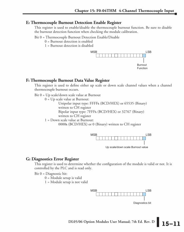
DL05/06 Option Modules User Manual; 7th Ed. Rev. D 15–11
Chapter 15: F0-04THM 4-Channel Thermocouple Input
E: Thermocouple Burnout Detection Enable RegisterThis register is used to enable/disable the thermocouple burnout function. Be sure to disable the burnout detection function when checking the module calibration.
Bit 0 = Thermocouple Burnout Detection Enable/Disable 0 = Burnout detection is enabled 1 = Burnout detection is disabled
F: Thermocouple Burnout Data Value RegisterThis register is used to define either up scale or down scale channel values when a channel thermocouple burnout occurs.
Bit 0 = Up scale/down scale value at Burnout 0 = Up scale value at Burnout: Unipolar input type: FFFFh (BCD/HEX) or 65535 (Binary) written to CH register Bipolar input type: 7FFFh (BCD/HEX) or 32767 (Binary) written to CH register 1 = Down scale value at Burnout: 0000h (BCD/HEX) or 0 (Binary) written to CH register
G: Diagnostics Error RegisterThis register is used to determine whether the configuration of the module is valid or not. It is controlled by the PLC and is read only.
Bit 0 = Diagnostic bit: 0 = Module setup is valid 1 = Module setup is not valid
MSB LSB
Burnout
Function
MSB LSB
Up scale/down scale Burnout value
MSB LSB
Diagnostics bit

DL05/06 Option Modules User Manual; 7th Ed. Rev. D15–12
Chapter 15: F0-04THM 4-Channel Thermocouple Input
Configuring the Module in Your Control ProgramDL05 Example 1
The example program below shows how to setup the F0–04THM for 4 input channels enabled, J type thermocouple on all 4 input channels, BCD channel data format, Fahrenheit (ºF) temperature scale, magnitude plus sign bit format, and burnout detection enabled with an up scale burnout specified. Place this rung anywhere in the ladder program or in the initial stage if you are using stage programming instructions.
This is all that is required to read the temperature or voltage input data into V-memory locations. Once the data is in V-memory you can perform mathematical calculations with the data, compare the data against preset values, etc. V2000 is used in the example but you can use any user V-memory location.
LDSP0
LD
LDAO2000
OUTV7701
This loads an octal value for the first V-memory location that will be used to store the incoming data. For example, the O2000 entered here usingthe LDA instruction would designate the following addresses:Ch1 – V2000/2001, Ch2 – V2002/2003, Ch3 – V2004/2005,
The octal address (O2000) is stored here. Special V–memory locationV7701 is assigned to the option slot and acts as a pointer, whichmeans the CPU will use the octal value in this location to determineexactly where to store the incoming data.
Special V-memory location assigned to the option slot that specifiesthe data format and the number of channels to scan.
Loads a constant that specifies the number of input channels to scan and the data format. The upper byte, most significant nibble (MSN)selects the data format (0 = BCD, 8 = binary). The LSN selects thenumber of channels (1, 2, 3 or 4).
- or -
The binary format is used for displaying data on some operatorinterface units. K8400 enables 4 channels in binary format.
LDK0
Loads a 0 into the accumulator to set the following parameters in (V7703 – V7706).
Special V–memory location assigned to the option slot that specifies thethermocouple input type or voltage range selection. CJC is disabled withvoltage selected. K0 selects J type thermocouple with CJC enabled.
K0400 K8400
OUTV7704
OUTV7700
OUTV7703
Special V–memory location assigned to the option slot that specifiesthe Units Code (temperature scale and data format) selections. K0 selects º F temperature scale and magnitude plus sign bit format.
OUTV7706
Special V–memory location assigned to the option slot that specifiesthe thermocouple up scale/down scale burnout value. K0 selects anup scale value at burnout. FFFFh for unipolar inputs and 7FFFh for
OUTV7705
Special V–memory location assigned to the option slot that specifiesthe thermocouple burnout detection enable/disable.K0 selects burnout detection enabled.
bipolar inputs at burnout. The value is written to the channel inputregister when a thermocouple burnout occurs.
See table on page 15-9 for selections.
See truth table on page 15-10 for selections.
Ch4 – V2006/2007. See note on page 15-9.

DL05/06 Option Modules User Manual; 7th Ed. Rev. D 15–13
Chapter 15: F0-04THM 4-Channel Thermocouple Input
DL05 Example 2The example program below shows how to setup the F0–04THM for 2 input channels enabled, use of a K type thermocouple on the first 2 input channels, BCD channel data format, Celsius (ºC) temperature scale, 2’s complement format, and burnout detection enabled with a down scale burnout specified. Again, place this rung in the ladder program or in the intial stage if you are using stage programming instructions.
LDSP0
LD
LDAO2000
OUTV7701
This loads an octal value for the first V-memory location that will be usedto store the incoming data. For example, the O2000 entered here usingthe LDA instruction would designate the following addresses:Ch1 – V2000/2001, Ch2 – V2002/2003
The octal address (O2000) is stored here. Special V–memory locationV7701 is assigned to the option slot and acts as a pointer, whichmeans the CPU will use the octal value in this location to determineexactly where to store the incoming data.
Special V-memory location assigned to the option slot that specifiesthe data format and the number of channels to scan.
Loads a constant that specifies the number of input channels to scanand the data format. The upper byte, most significant nibble (MSN)selects the data format (0 = BCD, 8 = binary). The LSN selects thenumber of channels (1, 2, 3 or 4).
- or -
The binary format is used for displaying data on some operatorinterface units. K8200 enables 2 channels in binary format.
LDK1
LDK3
Loads a constant that specifies the input type. K1 selects K typethermocouple with CJC enabled. Enter a K0–K14 to specify the input
Special V–memory location assigned to the option slot that specifiesthe thermocouple input type or voltage range selection. CJC is
K0200 K8200
OUTV7704
OUTV7700
OUTV7703
Loads a constant that specifies the Units Code (temperature scale anddata format). K3 selects º C and 2’s complement data format.
Special V–memory location assigned to the option slot that specifiesthe temperature scale and data format selections.
LDK0
Loads a constant that enables/disables the thermocouple burnoutdetection function. K0 selects burnout function enabled.
OUTV7705
Special V–memory location assigned to the option slot that specifiesthe thermocouple burnout detection enable/disable.
LDK1
OUTV7706
Loads a constant that specifies the thermocouple burnout data value atburnout. K1 specifies a down scale value of 0000h to be written to thechannel input register when a thermocouple burnout occurs.
Special V–memory location assigned to the option slot that specifies thethermocouple up scale/down scale burnout value. The value is writtento the channel input register when a thermocouple burnout occurs.
type. See table on page 15-9 for selections.
disabled when voltage is selected.
See truth table on page 15-10 for selections.
See note on page 15-9.
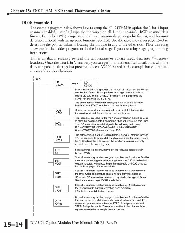
DL05/06 Option Modules User Manual; 7th Ed. Rev. D15–14
Chapter 15: F0-04THM 4-Channel Thermocouple Input
DL06 Example 1The example program below shows how to setup the F0–04THM in option slot 1 for 4 input channels enabled, use of a J type thermocouple on all 4 input channels, BCD channel data format, Fahrenheit (ºF ) temperature scale and magnitude plus sign bit format, and burnout detection enabled with an up scale burnout specified. Use the table shown on page 15–8 to determine the pointer values if locating the module in any of the other slots. Place this rung anywhere in the ladder program or in the initial stage if you are using stage programming instructions.
This is all that is required to read the temperature or voltage input data into V-memory locations. Once the data is in V-memory you can perform mathematical calculations with the data, compare the data against preset values, etc. V2000 is used in the example but you can use any user V-memory location.
LDSP0
LD
LDAO2000
OUTV701
This loads an octal value for the first V-memory location that will be used to store the incoming data. For example, the O2000 entered here usingthe LDA instruction would designate the following addresses:Ch1 – V2000/2001, Ch2 – V2002/2003, Ch3 – V2004/2005,
The octal address (O2000) is stored here. Special V–memory locationV701 is assigned to option slot 1 and acts as a pointer, which meansthe CPU will use the octal value in this location to determine exactlywhere to store the incoming data.
Special V-memory location assigned to option slot 1 that specifiesthe data format and the number of channels to scan.
Loads a constant that specifies the number of input channels to scan and the data format. The upper byte, most significant nibble (MSN)selects the data format (0 = BCD, 8 = binary). The LSN selects thenumber of channels (1, 2, 3 or 4).
- or -
The binary format is used for displaying data on some operatorinterface units. K8400 enables 4 channels in binary format.
LDK0
Loads a 0 into the accumulator to set the following parameters in (V703 – V706).
Special V–memory location assigned to option slot 1 that specifies thethermocouple input type or voltage range selection. CJC is disabled withvoltage selected. K0 selects J type thermocouple and CJC enabled.
K0400 K8400
OUTV704
OUTV700
OUTV703
Special V–memory location assigned to option slot 1 that specifiesthe Units Code (temperature scale and data format) selections. K0 selects º F temperature scale and magnitude plus sign bit format.
OUTV706
Special V–memory location assigned to option slot 1 that specifies thethermocouple up scale/down scale burnout value at burnout. K0selects an up scale value at burnout. FFFFh for unipolar inputs and7FFFh for bipolar inputs. The value is written to the channel input
OUTV705
Special V–memory location assigned to option slot 1 that specifiesthe thermocouple burnout detection enable/disable.K0 selects burnout detection enabled.
register when a thermocouple burnout occurs.
See table on page 15-9 for selections.
See truth table on page 15-10 for selections.
Ch4 – V2006/2007. See note on page 15-9.
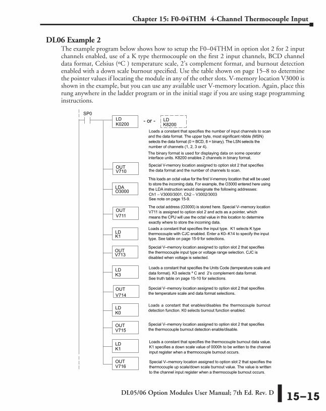
DL05/06 Option Modules User Manual; 7th Ed. Rev. D 15–15
Chapter 15: F0-04THM 4-Channel Thermocouple Input
DL06 Example 2The example program below shows how to setup the F0–04THM in option slot 2 for 2 input channels enabled, use of a K type thermocouple on the first 2 input channels, BCD channel data format, Celsius (ºC ) temperature scale, 2’s complement format, and burnout detection enabled with a down scale burnout specified. Use the table shown on page 15–8 to determine the pointer values if locating the module in any of the other slots. V-memory location V3000 is shown in the example, but you can use any available user V-memory location. Again, place this rung anywhere in the ladder program or in the initial stage if you are using stage programming instructions.
LDSP0
LD
LDAO3000
OUTV711
This loads an octal value for the first V-memory location that will be used to store the incoming data. For example, the O3000 entered here usingthe LDA instruction would designate the following addresses:Ch1 – V3000/3001, Ch2 – V3002/3003
The octal address (O3000) is stored here. Special V–memory locationV711 is assigned to option slot 2 and acts as a pointer, whichmeans the CPU will use the octal value in this location to determineexactly where to store the incoming data.
Special V-memory location assigned to option slot 2 that specifiesthe data format and the number of channels to scan.
Loads a constant that specifies the number of input channels to scan and the data format. The upper byte, most significant nibble (MSN)selects the data format (0 = BCD, 8 = binary). The LSN selects thenumber of channels (1, 2, 3 or 4).
- or -
The binary format is used for displaying data on some operatorinterface units. K8200 enables 2 channels in binary format.
LDK1
LDK3
Loads a constant that specifies the input type. K1 selects K typethermocouple with CJC enabled. Enter a K0–K14 to specify the input
Special V–memory location assigned to option slot 2 that specifiesthe thermocouple input type or voltage range selection. CJC is
K0200 K8200
OUTV714
OUTV710
OUTV713
Loads a constant that specifies the Units Code (temperature scale anddata format). K3 selects º C and 2’s complement data format.
Special V–memory location assigned to option slot 2 that specifiesthe temperature scale and data format selections.
LDK0
Loads a constant that enables/disables the thermocouple burnoutdetection function. K0 selects burnout function enabled.
OUTV715
Special V–memory location assigned to option slot 2 that specifiesthe thermocouple burnout detection enable/disable.
LDK1
OUTV716
Loads a constant that specifies the thermocouple burnout data value.K1 specifies a down scale value of 0000h to be written to the channelinput register when a thermocouple burnout occurs.
Special V–memory location assigned to option slot 2 that specifies thethermocouple up scale/down scale burnout value. The value is writtento the channel input register when a thermocouple burnout occurs.
type. See table on page 15-9 for selections.
disabled when voltage is selected.
See truth table on page 15-10 for selections.
See note on page 15-9.

DL05/06 Option Modules User Manual; 7th Ed. Rev. D15–16
Chapter 15: F0-04THM 4-Channel Thermocouple Input
Negative Temperature Readings with Magnitude Plus SignWith bipolar ranges, you need some additional logic to determine whether the value being returned represents a positive temperature/voltage or a negative temperature/voltage. There is a simple solution:
• If you are using bipolar ranges and you get a value greater than or equal to 8000h, the value is negative.
• If you get a value less than or equal to 7FFFh, the value is positive.
The sign bit is the most significant bit, which combines 8000h to the data value. If the value is greater than or equal to 8000h, you only have to mask the most significant bit and the active channel bits to determine the actual data value.
The following two programs show how you can accomplish this. The first example uses magnitude plus sign (binary) and the second example uses magnitude plus sign (BCD).
Since you always want to know when a value is negative, these rungs should be placed before any other operations that use the data, such as math instructions, scaling operations, and so forth. Also, if you are using stage programming instructions, these rungs should be in a stage that is always active. Note: you only need this logic for each channel that is using bipolar input signals. The examples only show two channels.
Magnitude Plus Sign (Binary)
SP1
OUTC1
LDV2000
OUTV2010
Load channel 1 data from V-memory into theaccumulator. Contact SP1 is always on.
Put the actual signal value in V2010. Now you can usethe data normally.
ANDDK7FFF
This instruction masks the sign bit of the binary data, ifit is set. Without this step, negative values will not becorrect so do not forget to include it.
V2000 K8000Channel 1 data is negative when C1 is on (a value of–1.0 reads as 8010, –2.0 is 8020, etc.).
SP1
OUTC2
LDV2002
OUTV2012
Load channel 2 from V-memory into the accumulator.Contact SP1 is always on.
Put the actual signal value in V2012. Now you can usethe data normally.
ANDDK7FFF
This instruction masks the sign bit of the binary data, ifit is set. Without this step, negative values will not becorrect so do not forget to include it.
V2002 K8000Channel 2 data is negative when C2 is on (a value of–1.0 reads as 8010, –2.0 is 8020, etc.).
M�
M�
Check Channel 1
Check Channel 2
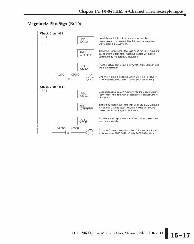
DL05/06 Option Modules User Manual; 7th Ed. Rev. D 15–17
Chapter 15: F0-04THM 4-Channel Thermocouple Input
Magnitude Plus Sign (BCD)
SP1
OUT
C1
LDDV2000
OUTDV2010
Load channel 1 data from V-memory into theaccumulator. Remember, the data can be negative.Contact SP1 is always on.
Put the actual signal value in V2010. Now you can usethe data normally.
ANDDK7FFFFFFF
This instruction masks the sign bit of the BCD data, if itis set. Without this step, negative values will not becorrect so do not forget to include it.
V2001 K8000
Check Channel 1
Check Channel 2
Channel 1 data is negative when C1 is on (a value of–1.0 reads as 8000 0010, –2.0 is 8000 0020, etc.).
SP1
OUT
C2
LDDV2002
OUTDV2012
Load channel 2 from V-memory into the accumulator.Remember, the data can be negative. Contact SP1 isalways on.
Put the actual signal value in V2012. Now you can usethe data normally.
ANDDK7FFFFFFF
This instruction masks the sign bit of the BCD data, if itis set. Without this step, negative values will not becorrect so do not forget to include it.
V2003 K8000Channel 2 data is negative when C2 is on (a value of–1.0 reads as 8000 0010, –2.0 is 8000 0020, etc.).
M
M

DL05/06 Option Modules User Manual; 7th Ed. Rev. D15–18
Chapter 15: F0-04THM 4-Channel Thermocouple Input
Module ResolutionModule Resolution 16-Bit (Unipolar Voltage Input)
Unipolar analog signals are converted into 65536 (216) counts ranging from 0 to 65535. For example, with a 0 to 156.25 mVDC signal range, 78 mVDC would be 32767. A value of 65535 represents the upper limit of the range.
Module Resolution 15-Bit Plus Sign (Bipolar Voltage Input)
The module has 16-bit unipolar or 15-bit + sign bipolar resolution. Bipolar analog signals are converted into 32768 (215) counts ranging from 0 to 32767. For example, with a –156.25 mVDC to 156.25 mVDC input signal range, 156.25 mVDC would be 32767. The bipolar ranges utilize a sign bit to provide 16-bit resolution. A value of 32767 can represent the upper limit of either side of the range. Use the sign bit to determine negative values.
0 65535327670 VDC
78
156.25mVDC
Counts
mVDC
Unipolar Resolution = H – L65535
H or L = high or low limit of the range
32767 327670
–156.25
0 VDC
156.25
Counts
mVDC
mVDC
(sign bit = 1) (sign bit = 0)
Bipolar Resolution = H – L32767
H or L = high or low limit of the range

DL05/06 Option Modules User Manual; 7th Ed. Rev. D 15–19
Chapter 15: F0-04THM 4-Channel Thermocouple Input
Analog Input Ladder Logic FilterPID Loops / Filtering
Please refer to the “PID Loop Operation” chapter in the DL06 or DL05 User Manual for information on the built-in PV filter (DL05/06) and the ladder logic filter (DL06 only) shown below. A filter must be used to smooth the analog input value when auto tuning PID loops to prevent giving a false indication of loop characteristics.
Smoothing the Input Signal (DL06 only)The filter logic can also be used in the same way to smooth the analog input signal to help stabilize PID loop operation or to stabilize the analog input signal value for use with an operator interface display, etc.
WARNING: The built-in and logic filters are not intended to smooth or filter noise generated by improper field device wiring or grounding. Small amounts of electrical noise can cause the input signal to bounce considerably. Proper field device wiring and grounding must be done before attempting to use the filters to smooth the analog input signal.
Using Binary Data Format
LDV2000
SUBRV1400
BTOR
SP1Loads the analog signal, which is in binary formatand has been loaded from V-memory locationV2000, into the accumulator. Contact SP1 isalways on.
Converts the binary value in the accumulatorto a real number.
Subtracts the real number stored in locationV1400 from the real number in the accumulator,and stores the result in the accumulator. V1400is the designated workspace in this example.
Multiplies the real number in the accumulator by0.2 (the filter factor), and stores the result in theaccumulator. This is the filtered value. The filterrange is 0.1 to 0.9. Smaller filter factorsincreases filtering. (1.0 eliminates filtering).
OUTDV1400
ADDRV1400
MULRR0.2
OUTV1402
RTOB
Adds the real number stored inlocation V1400 to the real numberfiltered value in the accumulator, andstores the result in the accumulator.
Copies the value in the accumulator tolocation V1400.
Converts the real number in theaccumulator to a binary value, andstores the result in the accumulator.
Loads the binary number filtered value fromthe accumulator into location V1402 to use inyour application or PID loop.

DL05/06 Option Modules User Manual; 7th Ed. Rev. D15–20
Chapter 15: F0-04THM 4-Channel Thermocouple Input
NOTE: Be careful not to do a multiple number conversion on a value. For example, if you are using the pointer method in BCD format to get the analog value, it must be converted to binary (BIN) as shown below. If you are using the pointer method in Binary format, the conversion to binary (BIN) instruction is not needed.
Using BCD Data Format
LDDV2000
SUBRV1400
BTOR
SP1
BIN
Loads the analog signal, which is in BCD formatand has been loaded from V-memory locationV2000, into the accumulator. Contact SP1 isalways on.
Converts a BCD value in the accumulator tobinary.
Converts the binary value in the accumulatorto a real number.
Subtracts the real number stored in locationV1400 from the real number in the accumulator,and stores the result in the accumulator. V1400is the designated workspace in this example.
Multiplies the real number in the accumulator by0.2 (the filter factor), and stores the result in theaccumulator. This is the filtered value. The filterrange is 0.1 to 0.9. Smaller filter factorsincreases filtering. (1.0 eliminates filtering).
OUTDV1400
ADDRV1400
MULRR0.2
OUTDV1402
BCD
RTOB
Adds the real number stored inlocation V1400 to the real numberfiltered value in the accumulator, andstores the result in the accumulator.
Copies the value in the accumulator tolocation V1400.
Converts the real number in theaccumulator to a binary value, andstores the result in the accumulator.
Converts the binary value in the accumulatorto a BCD number. Note: The BCD instructionis not needed for PID loop PV (loop PV is abinary number).
Loads the BCD number filtered value fromthe accumulator into location V1402 to use inyour application or PID loop.
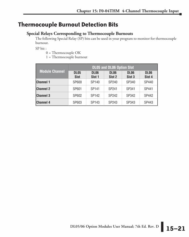
DL05/06 Option Modules User Manual; 7th Ed. Rev. D 15–21
Chapter 15: F0-04THM 4-Channel Thermocouple Input
Thermocouple Burnout Detection BitsSpecial Relays Corresponding to Thermocouple Burnouts
The following Special Relay (SP) bits can be used in your program to monitor for thermocouple burnout.
SP bit : 0 = Thermocouple OK 1 = Thermocouple burnout
Module ChannelDL05 and DL06 Option Slot
DL05 Slot
DL06 Slot 1
DL06 Slot 2
DL06 Slot 3
DL06 Slot 4
Channel 1 SP600 SP140 SP240 SP340 SP440
Channel 2 SP601 SP141 SP241 SP341 SP441
Channel 3 SP602 SP142 SP242 SP342 SP442
Channel 4 SP603 SP143 SP243 SP343 SP443


