DLDA (CBCGS MAY 2018) Q1] a) Write the entity declaration in VHDL for NOR gate. (02) Solution :- NOR Gate: A logic gate whose output logic is ‘1’ if and only if all of its inputs are logic ‘0’. Entity declaration of NOR gate Library IEEE; use IEEE.STD_LOGIC_1164.ALL; entity nor_df is Port (a: in STD_LOGIC; b: in STD_LOGIC; c: out STD_LOGIC); end nor_df; architecture Behavioral of nand_df is begin c<=a nor b; Q1] b) Add (22)10 to (56)10 in BCD. (02) Solution :- BCD of (22)10 is 00100010 BCD of (56)10 is 01010110 0 0 1 0 0 0 1 0 + 0 1 0 1 0 1 1 0 0 1 1 1 1 0 0 0 (22)10 + (56)10 = 01111000
Transcript
DLDA
(CBCGS MAY 2018)
Q1] a) Write the entity declaration in VHDL for NOR gate.
(02)
Solution :-
NOR Gate:
A logic gate whose output logic is ‘1’ if and only if all of its inputs are logic ‘0’.
Entity declaration of NOR gate
Library IEEE;
use IEEE.STD_LOGIC_1164.ALL;
entity nor_df is
Port (a: in STD_LOGIC;
b: in STD_LOGIC;
c: out STD_LOGIC);
end nor_df;
architecture Behavioral of nand_df
is
begin
c<=a nor b;
Q1] b) Add (22)10 to (56)10 in BCD.
(02)
Solution :-
BCD of (22)10 is 00100010
BCD of (56)10 is 01010110
0 0 1 0 0 0 1 0
+ 0 1 0 1 0 1 1 0
0 1 1 1 1 0 0 0
(22)10 + (56)10 = 01111000
Q1] c) Convert decimal 57 into binary, base 7 and hexadecimal.
(02)
Solution :-
Decimal 57 to binary
Decimal 57 to base 7
Decimal 57 to hexadecimal
Q1] d) Construct hamming code for 1010.
(02)
Solution :-
7 bit Hamming code is given as
D7 D6 D5 P4 D3 P2 P1
Given 4 bit is 1010 therefore it can be written as
P1: For P1 consider P1, D3, D5, D7
D3, D5, D7 = 011
For even parity set P1 = 0
1 0 1 P4 0 P2 P1
P1: For P2 consider P2, D3, D6, D7
D3, D6, D7 = 001
For even parity set P2 = 1
P1: For P1 consider P4, D5, D6, D7
D5, D6, D7 = 011
For even parity set P4 = 0
Therefore, hamming code for 1010 is given as 1010010.
Q1] e) Perform subtraction using 2’s complement for (10)10 - (7)10.
(02)
Solution :-
Binary representation of 7 is 0111
1’s complement of 7 is 1000
2’s complement of 7 is 1’s complement + 1
1 0 0 0
+ 1
1 0 0 1
Now adding 10 and 2’s complement of 7
1 0 1 0
+ 1 0 0 1
1 0 0 1 1
Discard carry 1
Therefore (10)10 - (7)10 = 0011 = (3)10.
Q1] f) State and prove De Morgan’s law.
(02)
Solution :-
Theorem 1:
1 0 1 0 0 1 0
Statement: The complement of the product of two or more variables is equal to the sum of the
components of the variables.
Logical expression: A. B̅̅ ̅̅ ̅ = A̅ + B̅
NAND is equal to BUBBLED OR.
A B A.B A. B̅̅ ̅̅ ̅ A̅ B̅ A̅ + B̅
0 0 0 1 1 1 1
0 1 0 1 1 0 1
1 0 0 1 0 1 1
1 1 1 0 0 0 0
From the above truth table we can see that A. B̅̅ ̅̅ ̅ = A̅ + B̅ Hence proved.
Theorem 2 :-
Statement: The complement of the sum of two or more variables is equal to the product of the
complement of the variables
Logical expression: 𝐴 + 𝐵̅̅ ̅̅ ̅̅ ̅̅ = �̅�. �̅�
NOR is equal to BUBBLED AND.
A B A + B A + B̅̅ ̅̅ ̅̅ ̅ A̅ B̅ A̅. B̅
0 0 0 1 1 1 1
0 1 1 0 1 0 0
1 0 1 0 0 1 0
1 1 1 0 0 0 0
From the above truth table we can see that 𝐴 + 𝐵̅̅ ̅̅ ̅̅ ̅̅ = �̅�. �̅� Hence proved.
Q1] g) Convert (77)10 into Excess 3 code.
(02)
Solution :-
Excess 3 code is 3 added to BCD.
BCD of 77 is 0111 0111 and 0f 3 is 0011
0 1 1 1 0 1 1 1
+ 0 0 1 1 0 0 1 1
1 0 1 0 1 0 1 0
Excess 3 code of 77 is 10101010
Q1] h) Perform addition of (34)8 and (62)8.
(02)
Solution :-
(34)8 + (62)8
3 4
+ 6 2
1 1 6
In the above sum 6 + 3 is greater than 7 hence can’t be represented as octal therefore we need to
divide it with 8
Remainder is the sum and the quotient is carry.
Therefore, we get (34)8 + (62)8 = (116)8.
Q1] i) Find 8’s complement of the number (37)8 and (301)8.
(02)
Solution :-
To find 8’s complement we first need to find 7’s complement and then add 1 to it.
7’s complement of 37 is obtain by subtracting 37 from 77
i) 7 7
+ 3 7
4 0 7’s complement
+ 1
4 1 8’s complement
ii) 7 7 7
+ 3 0 1
4 7 6 7’s complement
+ 1
4 7 7 8’s complement
Q1] j) Explain ASCII code in brief.
(02)
Solution :-
ASCII was developed by the American National Standards Institute (ANSI). Pronounced ask-ee, ASCII
is the acronym for the American Standard Code for Information Interchange.
It is a code for representing 128 English characters as numbers.
Technically, ASCII is 7-bit representing only 128 characters (0-127). The range 0-31 are control
characters, with 32-127 representing alphabetical characters from A to Z, numerals from 0 to 9 and
punctuation marks (though not in that order).
For example, the ASCII code for uppercase M is 77.
Most computers use ASCII codes to represent text, which makes it possible to transfer data from one
computer to another.
Text files stored in ASCII format are sometimes called ASCII files. Text editors and word
processors are usually capable of storing data in ASCII format, although ASCII format is not always
the default storage format.
Q2] a) Simplify the following equation using K map to obtain SOP equation and realize the
In full adder there are 3 input A, B and Cin and they are added and generates two output S and Cout.
S is the sum of A, B and Cin and Cout is the carry generated by adding 3 input’s.
Full Adder Implementation using 8:1 MUX
An 8:1 multiplexer consists of eight data inputs I0 to I7, three input select lines A, B and C and a single
output line Y. Depending on the select lines combinations, multiplexer decodes the inputs.
Since the number of input data bits given to the MUX are eight therefore 3 bits (23=8) are needed to
select one of the eight data bits. That is there is 3 select lines in 8:1 MUX.
Since in full adder there are 2 output, we need two 8:1 multiplexer. Output of 1st multiplexer is sum
of adder and output of 2nd multiplexer is carry generated of full adder.
Fig. Full Adder using 8:1 MUX
As we can see in the above diagram there are 3 select lines A, B and C. there are 7 input I0 to I7.
The input is connected to 0 or 1 depending upon the value given in truth table.
The select lines of both multiplexer is connected to same input.
Q3] a) Obtain the minimal expression using Quine Mc-Cluskey method
F(A,B,C,D) = 𝜮m(1,2,3,5,6,10.11,13,14) + d(4,7)
(10)
Solution :-
Table 1
Group Minterm Binary Representation
A B C D
0 M1 0 0 0 1
M2 0 0 1 0
M4* 0 1 0 0
1 m3 0 0 1 1
m5 0 1 0 1
m6 0 1 1 0
m10 1 0 1 0
2 m13 1 1 0 1
m14 1 1 1 0
m7* 0 1 1 1
Table 2
Group Minterm Binary Representation
A B C D
0 m1-m3 0 0 _ 1
m1-m5 0 _ 0 1
m2-m3 0 0 1 _
m2-m6 0 _ 1 0
m2-m10 _ 0 1 0
m4-m5* 0 1 0 _
m4-m6* 0 1 _ 0
1 m3-m7* 0 _ 1
M5-m13 _ 1 0 1
m5-m7* 0 1 _ 1
m6-m14 _ 1 1 0
m6-m7* 0 1 1 _
m10-m14 1 _ 1 0
Table 3
Group Minterm Binary Representation
A B C D
0
m1-m3-m5-m7 0 _ _ 1
M1-m5-m3-m7 0 _ _ 1
M1-m5-m10-m14 _ _ _ _
M2-m3-m6-m7 0 _ 1 _
M2-m6-m3-m7 0 _ 1 _
M2-m6-m10-m14 _ _ 1 0
M2-m10-m5=m13 _ _ _ _
M2-m10-m6-m14 _ _ 1 0
M4-m5-m6-m7 0 1 _ _
M4-m6-m5-m7 0 1 _ _
PI Decimal of PI 1 2 3 5 6 10 13 14 4 7
�̅�𝐷 M1 m3 m5 m7 ⊗ X X X
�̅�𝐶 M2 m3 m6 m7 X X X X
𝐶�̅� M2-m6-m10-m14 X X ⊗ ⊗
�̅�𝐵 M4-m5-m6=m7 X X ⊗ X
Y = �̅�𝐃 + 𝐂𝐃̅̅ ̅̅ + �̅�B
Q3] b) What is race around condition? How to overcome it?
(10)
Solution:-
The race around condition occurs in JK flipflop when both the inputs are high that is J=K=1 normally in level triggered JK flipflop.
Fig.3.1 Race around condition
The above figure shows the race around condition in JK Flipflop when J=K=1.
This may lead to unpredictable output when clock disables and it is called as race around condition.
This can be avoided by
1. Using edge triggered JK flipflop 2. Using Master Slave JK flipflop
In edge triggered JK flipflop, race condition is avoided as the enable input of the clock remains active
only for a short time.
In master slave flipflop master and slave are inverted clock so that only one will be active at a time.
During the high of the clock, output will be toggled and will remain at the output of master but could
not be followed by slave as it is disabled. So, output of slave remains same as earlier and toggled
output remains at master. When clock is low master is deactivated and slave is enabled which only
follows the output of master. So at the end of one complete clock we just have one toggled output
and race around condition is avoided.
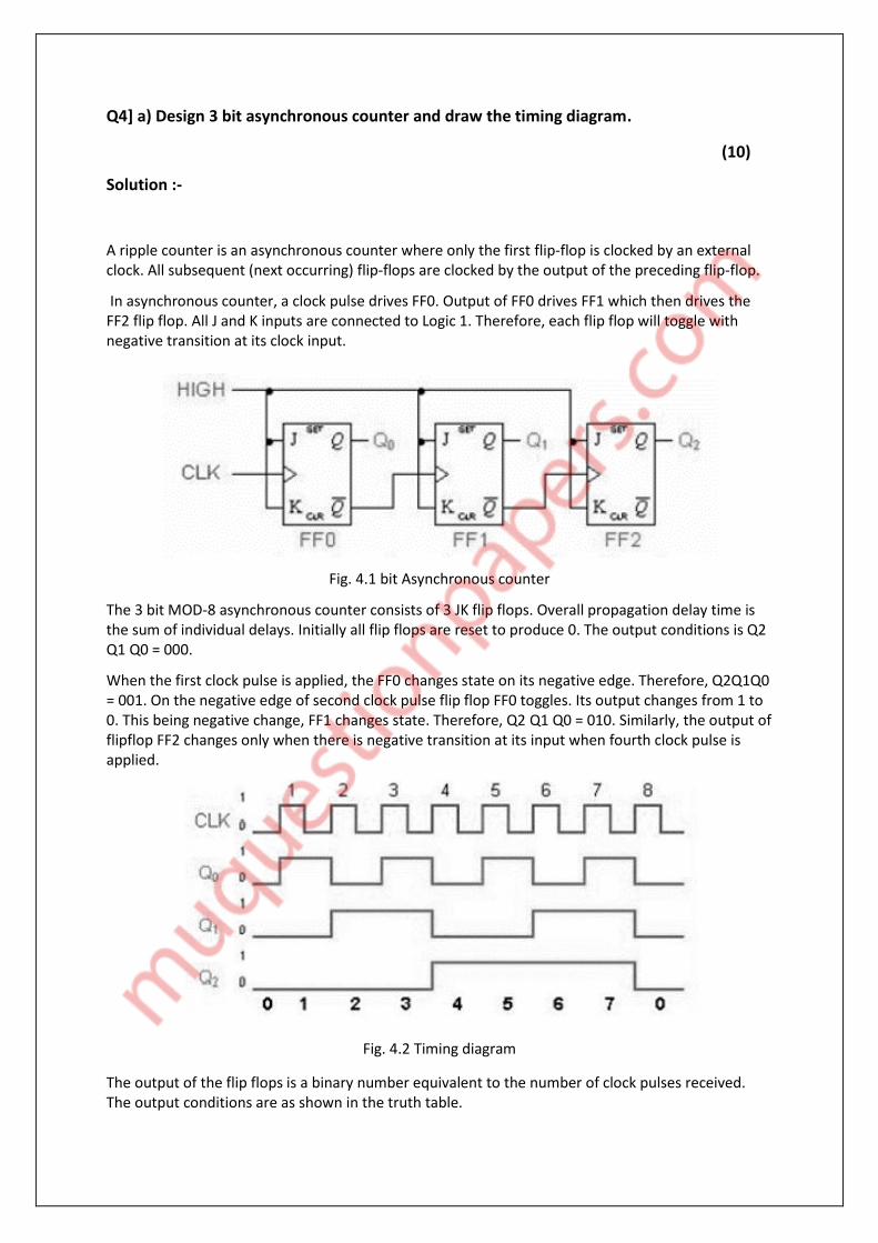
Q4] a) Design 3 bit asynchronous counter and draw the timing diagram.
(10)
Solution :-
A ripple counter is an asynchronous counter where only the first flip-flop is clocked by an external clock. All subsequent (next occurring) flip-flops are clocked by the output of the preceding flip-flop.
In asynchronous counter, a clock pulse drives FF0. Output of FF0 drives FF1 which then drives the FF2 flip flop. All J and K inputs are connected to Logic 1. Therefore, each flip flop will toggle with negative transition at its clock input.
Fig. 4.1 bit Asynchronous counter
The 3 bit MOD-8 asynchronous counter consists of 3 JK flip flops. Overall propagation delay time is the sum of individual delays. Initially all flip flops are reset to produce 0. The output conditions is Q2 Q1 Q0 = 000.
When the first clock pulse is applied, the FF0 changes state on its negative edge. Therefore, Q2Q1Q0 = 001. On the negative edge of second clock pulse flip flop FF0 toggles. Its output changes from 1 to 0. This being negative change, FF1 changes state. Therefore, Q2 Q1 Q0 = 010. Similarly, the output of flipflop FF2 changes only when there is negative transition at its input when fourth clock pulse is applied.
Fig. 4.2 Timing diagram
The output of the flip flops is a binary number equivalent to the number of clock pulses received. The output conditions are as shown in the truth table.
Counter State
Q2 Q1 Qo
0 0 0 0
1 0 0 1
2 0 1 0
3 0 1 1
4 1 0 0
5 1 0 1
6 1 1 0
7 1 1 1
On the negative edge of eighth pulse, counter is reset. The counter acts as a frequency divider. FF0 divides clock frequency by 2, FF1 divides clock frequency by 4, FF2 divides clock frequency by 8. If n flip flops are cascaded, we get 2n output conditions. The largest binary number counted by n cascaded flip flops has a decimal equivalent of 2n −1. MOD-8 counter has count of the largest binary number 111 which has decimal equivalent of 23−1=7.
Q4] b) Convert JK flipflop to SR flipflop and D flipflop.
(10)
Solution :-
JK to SR
a) Excitation Table
Input’s Present State Next State Flip Flop Input
S R Qn Qn+1 J K
0 0 0 0 0 X
0 0 1 1 X 0
0 1 0 0 X X
0 1 1 0 X 1
1 0 0 1 1 X
1 0 1 1 X 0
1 1 0 X X X
1 1 1 X X X
b) K- map simplification
For J
For K
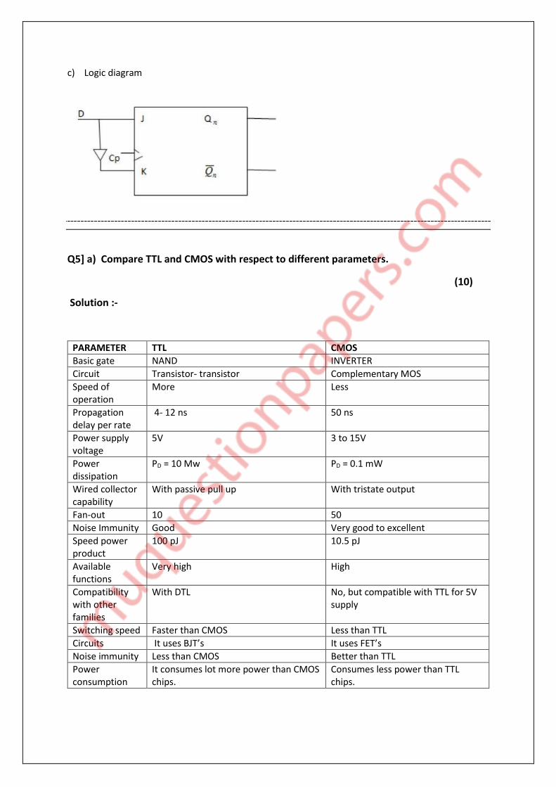
c) Logic diagram
JK to D
a) Excitation Table
Input Present State Next State Flip Flop Input
D Qn Qn+1 J K
0 0 0 0 X
0 1 0 X 1
1 0 1 1 X
1 1 1 X 0
b) K-map simplification
For J
J = D
For K
c) Logic diagram
Q5] a) Compare TTL and CMOS with respect to different parameters.
(10)
Solution :-
PARAMETER TTL CMOS
Basic gate NAND INVERTER
Circuit Transistor- transistor Complementary MOS
Speed of operation
More Less
Propagation delay per rate
4- 12 ns 50 ns
Power supply voltage
5V 3 to 15V
Power dissipation
PD = 10 Mw PD = 0.1 mW
Wired collector capability
With passive pull up With tristate output
Fan-out 10 50
Noise Immunity Good Very good to excellent
Speed power product
100 pJ 10.5 pJ
Available functions
Very high High
Compatibility with other families
With DTL No, but compatible with TTL for 5V supply
Switching speed Faster than CMOS Less than TTL
Circuits It uses BJT’s It uses FET’s
Noise immunity Less than CMOS Better than TTL
Power consumption
It consumes lot more power than CMOS chips.
Consumes less power than TTL chips.
Q5 b) Explain the features of VHDL and its modeling styles.
(10)
Solution:-
VHDL stands for very high-speed integrated circuit hardware description language. This language was
first introduced in 1981 for the department of Defense (DoD) under the VHSIC program.
Features of VHDL are as follows:
1) Designs are organized hierarchically.
2) Each design element has:
i) A well-defined interface.
ii) A precise behavioral specification using either algorithmic description or hardware
structural description.
3) Models concurrency, timing, and clocking:
i) Handles asynchronous and synchronous circuits
ii) Designs can be simulated.
4) Language is not case sensitive.
5) A formal language for specifying the behavior and structure digital circuit.
Modeling styles: Modeling Style means, that how we Design our Digital IC's in Electronics. With the
help of modeling style we describe the Design of our Electronics.
Normally we use Three type of Modeling Style in VHDL -
• Data Flow Modeling Style.
• Behavior Modeling Style.
• Structural Modeling Style.
Data Flow Modeling Style – Dataflow system describes a system in terms of how data flows through
the system. Data dependencies in the description match those in atypical hardware implementation.
A dataflow description directly implies a corresponding gate level implementation.
Dataflow descriptions consist of one or more concurrent signal assignment situation
Behavior Modeling Style – A behavioral description describes a system’s behavior or function in an
algorithmic fashion.
Behavioral style is the most abstract style. The description is abstract in the sense that it does not
directly imply a particular gate-level implementation.
Behavioral style consists of one or more process statements. Each process statement is a single
concurrent statement that itself contains one or more sequential statements.
Sequential statements are executed sequentially statements by a simulator, the same as the execution
of sequential statements in a conventional programming language.
Structural Modeling Style – In structural style of modelling, an entity is described as a set of
interconnected components.
The top-level design entity’s architecture describes the interconnection of lower level design entities.
Each lower level entity can, in turn, be described as an interconnection of design entities at the next-
lower level, and so on.
Structural style is most useful and efficient when a complex system is described as an interconnection
of moderately complex design entities. This approach allows each design entity to be independently
designed and verified before being used in the higher-level description.
Q6] a) Moore and Mealy machine.
(05)
Solution :-
Moore Machines: Moore machines are finite state machines with output value and its output depends only on present state. It can be defined as (Q, q0, ∑, O, δ, λ) where: • Q is finite set of states. • q0 is the initial state. • ∑ is the input alphabet. • O is the output alphabet. • δ is transition function which maps Q×∑ → Q. • λ is the output function which maps Q → O.
Figure 1 In the moore machine shown in Figure 1, the output is represented with each input state separated by /. The length of output for a moore machine is greater than input by 1.
• Input: 11 • Transition: δ (q0,11)=> δ(q2,1)=>q2 • Output: 000 (0 for q0, 0 for q2 and again 0 for q2)
Mealy Machines: Mealy machines are also finite state machines with output value and its output depends on present state and current input symbol. It can be defined as (Q, q0, ∑, O, δ, λ’) where: • Q is finite set of states. • q0 is the initial state. • ∑ is the input alphabet. • O is the output alphabet. • δ is transition function which maps Q×∑ → Q. • ‘λ’ is the output function which maps Q×∑→ O.
Figure 2 In the mealy machine shown in Figure 1, the output is represented with each input symbol for each state separated by /. The length of output for a mealy machine is equal to the length of input.
• Input:11 • Transition: δ (q0,11)=> δ(q2,1)=>q2 • Output: 00 (q0 to q2 transition has Output 0 and q2 to q2 transition also has Output 0)
Q6] b) Sequence generator.
(05)
Solution :-
the sequence generators are nothing but a set of digital circuits which are designed to result in a
specific bit sequence at their output. There are several ways in which these circuits can be designed
including those which are based on multiplexers and flip-flops.
A circuit which generates a prescribed sequence of bits, in synchronization with a clock, is referred
to as a sequence generator such generator can be used as:
The basic structure of a sequence generator is shown in diagram below:
The output Y of the next state decoder is function of QN-2, QN-1 …….. Q1, Q0. This system is similar
to a ring counter or twisted ring counter which are special case of sequence generator, the design of
the decoder will be clear.
Q6] c) Universal shift register.
(05)
Solution:-
A Universal shift register is a register which has both the right shift and left shift with parallel load capabilities. Universal shift registers are used as memory elements in computers. A Unidirectional shift register is capable of shifting in only one direction. A bidirectional shift register is capable of shifting in both the directions. The Universal shift register is a combination design of bidirectional shift register and a unidirectional shift register with parallel load provision. n-bit universal shift register – A n-bit universal shift register consists of n flip-flops and n 4×1 multiplexers. All the n multiplexers share the same select lines(S1 and S0)to select the mode in which the shift register operates. The select inputs select the suitable input for the flip-flops. The working of the Universal shift register depends on the inputs given to the select lines.
The register operations performed for the various inputs of select lines are as follows:
S1 S0 REGISTER OPERATION
0 0 No changes
0 1 Shift Right
1 0 Shift Left
1 1 Parallel Load
Q6] d) Priority Encoder.
(05)
Solution :-
The priority encoders output corresponds to the currently active input which has the highest priority.
So, when an input with a higher priority is present, all other inputs with a lower priority will be ignored.
A priority encoder provides n bits of binary coded output representing the position of the highest order active input of 2ninputs. If two or more inputs are high at the same time, the input having the highest priority will take precedence.
Fig.6.d Priority Encoder
A 4-to-2 priority encoder takes 4 input bits and produces 2 output bits as shown in figure 6.4. In this
truth table, for all the non-explicitly defined input combinations (i.e. inputs containing 2, 3, or 4 high
bits) the lower priority bits are shown as don't cares (X). Similarly, when the inputs are 0000, the
outputs are not valid and therefore they are XX.
Truth table for 4 bit input to priority encoder:
I3 I2 I1 I0 Y1 Y0
0 0 0 0 X X
0 0 0 1 0 0
0 0 1 X 0 1
0 1 X X 1 0
0 1 X X 1 0
1 X X X 1 1
From this truth table, we use the Karnaugh Map to minimize the logic to the following Boolean
expressions:
Y1 = I2 + I3
Y0 = I3 + I2 X I1
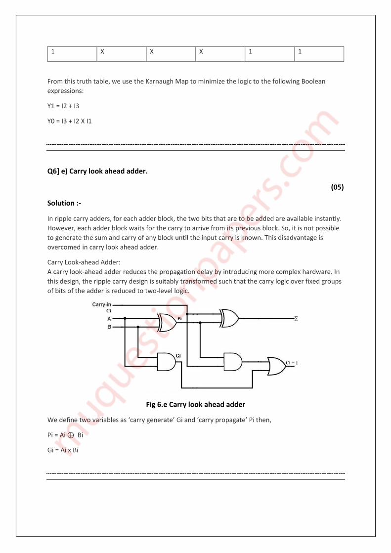
Q6] e) Carry look ahead adder.
(05)
Solution :-
In ripple carry adders, for each adder block, the two bits that are to be added are available instantly.
However, each adder block waits for the carry to arrive from its previous block. So, it is not possible
to generate the sum and carry of any block until the input carry is known. This disadvantage is
overcomed in carry look ahead adder.
Carry Look-ahead Adder:
A carry look-ahead adder reduces the propagation delay by introducing more complex hardware. In
this design, the ripple carry design is suitably transformed such that the carry logic over fixed groups
of bits of the adder is reduced to two-level logic.
Fig 6.e Carry look ahead adder
We define two variables as ‘carry generate’ Gi and ‘carry propagate’ Pi then,