106
Copyright © 2013 ARM. All rights reserved. ARM DDI 0521A (ID051113) CoreLink ™ MMU-401 System Memory Management Unit Revision: r0p0 Technical Reference Manual

CoreLink™ MMU-401 System MemoryManagement Unit
Revision: r0p0
Technical Reference Manual
Copyright © 2013 ARM. All rights reserved.ARM DDI 0521A (ID051113)

CoreLink MMU-401 System Memory Management Unit Technical Reference Manual
Copyright © 2013 ARM. All rights reserved.
Release Information
The following changes have been made to this book.
Proprietary Notice
Words and logos marked with ® or ™ are registered trademarks or trademarks of ARM® in the EU and other countries, except as otherwise stated below in this proprietary notice. Other brands and names mentioned herein may be the trademarks of their respective owners.
Neither the whole nor any part of the information contained in, or the product described in, this document may be adapted or reproduced in any material form except with the prior written permission of the copyright holder.
The product described in this document is subject to continuous developments and improvements. All particulars of the product and its use contained in this document are given by ARM in good faith. However, all warranties implied or expressed, including but not limited to implied warranties of merchantability, or fitness for purpose, are excluded.
This document is intended only to assist the reader in the use of the product. ARM Limited shall not be liable for any loss or damage arising from the use of any information in this document, or any error or omission in such information, or any incorrect use of the product.
Confidentiality Status
This document is Non-Confidential. The right to use, copy and disclose this document may be subject to license restrictions in accordance with the terms of the agreement entered into by ARM and the party that ARM delivered this document to.
Product Status
The information in this document is final, that is for a developed product.
Web Address
http://www.arm.com
Change history
Issue Confidentiality Change
14 March 2013 A Non-Confidential First release for r0p0.
ARM DDI 0521A Copyright © 2013 ARM. All rights reserved. iiID051113 Non-Confidential
ContentsCoreLink MMU-401 System Memory Management Unit Technical Reference Manual
PrefaceAbout this book ........................................................................................................... viFeedback .................................................................................................................... ix
Chapter 1 Introduction1.1 About the MMU-401 ................................................................................................. 1-21.2 Features of the MMU-401 ........................................................................................ 1-41.3 Implementation options for synthesis ...................................................................... 1-51.4 Product revisions ..................................................................................................... 1-8
Chapter 2 Functional Description2.1 Interfaces ................................................................................................................. 2-22.2 Stream ID ................................................................................................................. 2-72.3 Security determination ............................................................................................. 2-82.4 Hit-Under-Miss ......................................................................................................... 2-92.5 Fault handling ........................................................................................................ 2-102.6 Dynamic programming ........................................................................................... 2-11
Chapter 3 Programmers Model3.1 About the programmers model ................................................................................ 3-23.2 The MMU-401 address map .................................................................................... 3-33.3 Register summary .................................................................................................... 3-53.4 Global register space 0 .......................................................................................... 3-113.5 Global register space 1 .......................................................................................... 3-333.6 Integration registers ............................................................................................... 3-363.7 Performance monitoring registers .......................................................................... 3-39
ARM DDI 0521A Copyright © 2013 ARM. All rights reserved. iiiID051113 Non-Confidential

Contents
3.8 Security state determination address space .......................................................... 3-463.9 Peripheral and component identification registers ................................................. 3-483.10 Translation context-bank registers ......................................................................... 3-52
Appendix A Signal DescriptionsA.1 Clock and resets ...................................................................................................... A-2A.2 AXI3 signals ............................................................................................................. A-3A.3 AXI4 signals ............................................................................................................. A-8A.4 ACE-Lite signals .................................................................................................... A-12A.5 APB signals .......................................................................................................... A-17A.6 LPI signals ............................................................................................................. A-18A.7 Miscellaneous signals ............................................................................................ A-19
Appendix B Revisions
ARM DDI 0521A Copyright © 2013 ARM. All rights reserved. ivID051113 Non-Confidential

Preface
This preface introduces the CoreLink MMU-401 System Memory Management Unit (MMU-401) Technical Reference Manual in the following sections:• About this book on page vi.• Feedback on page ix.
ARM DDI 0521A Copyright © 2013 ARM. All rights reserved. vID051113 Non-Confidential
Preface
About this bookThis book is for the MMU-401.
Product revision status
The rnpn identifier indicates the revision status of the product described in this book, where:rn Identifies the major revision of the product.pn Identifies the minor revision or modification status of the product.
Intended audience
This book is written for system designers, system integrators, and programmers who are designing or programming a device that uses the MMU-401.
Using this book
This book is organized into the following chapters:
Chapter 1 Introduction Read this for an introduction to the MMU-401 and its features.
Chapter 2 Functional Description Read this for an overview of the major functional blocks and the operation of the MMU-401.
Chapter 3 Programmers Model Read this for a description of the MMU-401 memory map and registers.
Appendix A Signal Descriptions Read this for a description of the MMU-401 signals.
Appendix B Revisions Read this for a description of the technical changes between released issues of this book.
Glossary
The ARM Glossary is a list of terms used in ARM documentation, together with definitions for those terms. The ARM Glossary does not contain terms that are industry standard unless the ARM meaning differs from the generally accepted meaning.
See ARM Glossary, http://infocenter.arm.com/help/topic/com.arm.doc.aeg0014-/index.html.
Conventions
Conventions that this book can use are described in:• Typographical conventions on page vii.• Timing diagrams on page vii.• Signals on page viii.
ARM DDI 0521A Copyright © 2013 ARM. All rights reserved. viID051113 Non-Confidential

Preface
Typographical conventions
The following table describes the typographical conventions:
Timing diagrams
The figure named Key to timing diagram conventions explains the components used in timing diagrams. Variations, when they occur, have clear labels. You must not assume any timing information that is not explicit in the diagrams.
Shaded bus and signal areas are undefined, so the bus or signal can assume any value within the shaded area at that time. The actual level is unimportant and does not affect normal operation.
Key to timing diagram conventions
Typographical conventions
Style Purpose
italic Introduces special terminology, denotes cross-references, and citations.
bold Highlights interface elements, such as menu names. Denotes signal names. Also used for terms in descriptive lists, where appropriate.
monospace Denotes text that you can enter at the keyboard, such as commands, file and program names, and source code.
monospace Denotes a permitted abbreviation for a command or option. You can enter the underlined text instead of the full command or option name.
monospace italic Denotes arguments to monospace text where the argument is to be replaced by a specific value.
monospace bold Denotes language keywords when used outside example code.
<and> Encloses replaceable terms for assembler syntax where they appear in code or code fragments. For example:MRC p15, 0 <Rd>, <CRn>, <CRm>, <Opcode_2>
SMALL CAPITALS Used in body text for a few terms that have specific technical meanings, that are defined in the ARM glossary. For example, IMPLEMENTATION DEFINED, IMPLEMENTATION SPECIFIC, UNKNOWN, and UNPREDICTABLE.
Clock
HIGH to LOW
Transient
HIGH/LOW to HIGH
Bus stable
Bus to high impedance
Bus change
High impedance to stable bus
ARM DDI 0521A Copyright © 2013 ARM. All rights reserved. viiID051113 Non-Confidential

Preface
Signals
The signal conventions are:
Signal level The level of an asserted signal depends on whether the signal is active-HIGH or active-LOW. Asserted means:• HIGH for active-HIGH signals.• LOW for active-LOW signals.
Lower-case n At the start or end of a signal name denotes an active-LOW signal.
Additional reading
This section lists publications by ARM and by third parties.
See Infocenter, http://infocenter.arm.com, for access to ARM documentation.
ARM publications
This book contains information that is specific to this product. See the following documents for other relevant information:
• CoreLink MMU-401 System Memory Management Unit Implementation Guide (ARM DII 0292).
• CoreLink MMU-401 System Memory Management Unit Integration Manual (ARM DIT 0052).
• CoreLink MMU-401 System Memory Management Unit AMBA® Designer (ADR-400) User Guide Supplement (ARM DSU 0032).
• ARM System Memory Management Unit Architecture Specification (ARM IHI 0062).
• ARM System Memory Management Unit Architecture Specification 64KB Translation Granule Supplement (ARM IHI 0067).
• CoreSight™ Architecture Specification (ARM IHI 0029).
• ARM Architecture Reference Manual, ARMv7-A and ARMv7-R edition (ARM DDI 0406).
• ARM Architecture Reference Manual, ARMv8, for ARMv8-A architecture profile (ARM DDI 0487).
• AMBA AXI™ and ACE™ Protocol Specification, AXI3™, AXI4™, and AXI4-Lite™, ACE and ACE-Lite™ (ARM IHI 0022).
• AMBA Specification (ARM IHI 0011).
• AMBA 3 APB™ Protocol Specification (ARM IHI 0024).
ARM DDI 0521A Copyright © 2013 ARM. All rights reserved. viiiID051113 Non-Confidential

Preface
FeedbackARM welcomes feedback on this product and its documentation.
Feedback on this product
If you have any comments or suggestions about this product, contact your supplier and give:• The product name.• The product revision or version.• An explanation with as much information as you can provide. Include symptoms and
diagnostic procedures if appropriate.
Feedback on content
If you have comments on content then send an e-mail to [email protected]. Give:• The title.• The number, ARM DDI 0521A.• The page numbers to which your comments apply.• A concise explanation of your comments.
ARM also welcomes general suggestions for additions and improvements.
Note ARM tests the PDF only in Adobe Acrobat and Acrobat Reader, and cannot guarantee the quality of the represented document when used with any other PDF reader.
ARM DDI 0521A Copyright © 2013 ARM. All rights reserved. ixID051113 Non-Confidential

Chapter 1 Introduction
This chapter provides an overview of the MMU-401, described in the following sections:• About the MMU-401 on page 1-2.• Features of the MMU-401 on page 1-4.• Implementation options for synthesis on page 1-5.• Product revisions on page 1-8.
ARM DDI 0521A Copyright © 2013 ARM. All rights reserved. 1-1ID051113 Non-Confidential
Introduction
1.1 About the MMU-401The MMU-401 controller provides the address translation that a hypervisor needs to virtualize multiple guest operating systems (OSs). It does so by translating the intermediate physical address (IPA) defined by an OS to the physical address (PA) defined by the hypervisor. If required, the MMU-401 can modify the memory attributes defined by the OS.
Typically:
• An OS is unaware that it is operating under the control of a hypervisor.
• Therefore, the OS performs its operations assuming that it is mapping a virtual addresses to a physical addresses directly (that is without the hypervisor control). The hypervisor performs the actual IPA to PA address mapping and hides the mapping information from the OS.
The addresses generated by the OS are in the IPA address space that must be translated by the MMU-401 controller when they are accessed.
The MMU-401 controller provides address virtualization to processors and other bus masters in a system. It also provides support for the 64KB translation granule. Using a larger granule size can significantly improve the address translation performance because a TLB entry can cover a large page size.
The implementer of the MMU-401 controller can optimize the features, performance, and gate count required for the intended applications.
ARM DDI 0521A Copyright © 2013 ARM. All rights reserved. 1-2ID051113 Non-Confidential

Introduction
Figure 1-1 shows the MMU-401 in an example ARM processor and the CoreLink Cache Coherent Interconnect-400 (CCI-400) system, performing address translation functions for a DMA.
Figure 1-1 MMU-401 in system context
The MMU-401 checks access permissions, translates addresses, and provides the capability to generate or merge access attributes. The Translation Look-aside Buffer (TLB) maintenance is done through Distributed Virtual-memory Messaging (DVM) signalling or through programmable control registers.
The following are example masters for the MMU-401:• Graphics Processor Units (GPUs).• Video engines.• Direct Memory Access (DMA) controllers.• Color LCD (CLCD) controllers.• Network controllers.
Each transaction received by the MMU-401 is passed through the following logical processing steps:• Security state determination.• Context determination.• Page table walk, if the translation is not cached in the TLB.• Protection checks.• Attribute generation or merging, depending on the programming.
You can configure the MMU-401 to bypass the translation process for a transaction or to fault a transaction regardless of the translation state.
Cache Coherent Interconnect
DMA
AsynchronousBridge
MMU-401Generic
Interrupt Controller
Cortex-A15 Cortex-A15
IRQ IRQ FIQFIQ
ACE ACE
ACE ACE
ACE-Lite
SMMU IRQ
DMA IRQ
ACE-Lite + DVM ACE-Lite + DVM ACE-Lite + DVM
ACE-Lite ACE-Lite ACE-Lite
Dynamic Memory Controller Network InterconnectACE-Lite
PHY
APB
APB APBAXI4 APB
DDR2/3 or LPDDR2
AX14
APB
ARM DDI 0521A Copyright © 2013 ARM. All rights reserved. 1-3ID051113 Non-Confidential
Introduction
1.2 Features of the MMU-401The MMU-401 provides the following functionality:• Conversion from 32-40 bit Large Physical Address Extension (LPAE) addresses for 32-bit
IO devices. — For more information on LPAE addresses, see the ARM Architecture Reference
Manual ARMv7-A and ARMv7-R edition and the ARM Architecture Reference Manual, ARMv8, for ARMv8-A architecture profile.
• Multiple transaction contexts that can apply to address translations for specific streams of transactions.— Up to eight configurable contexts are supported. Each context is mapped by using
an input stream ID from the master device that requires the address translations.• Stage 2 address translations for OS level IPA to PA translations in the ARM LPAE format.
— For more information on LPAE addresses, see the ARM Architecture Reference Manual ARMv7-A and ARMv7-R edition and the ARM Architecture Reference Manual, ARMv8, for ARMv8-A architecture profile.
• Translation support for the following:— ARMv7 4KB, 2MB, and 1GB page sizes.— ARMv8 64KB and 512MB page sizes.
For more information on ARM v7 and ARM v8 virtualization extensions, LPAE addresses, see the ARM Architecture Reference Manual ARMv7-A and ARMv7-R edition and the ARM Architecture Reference Manual, ARMv8, for ARMv8-A architecture profile.
• Provides page table walk (PTW) cache for storing intermediate PTW data.• Caching of PTW entries in the TLB.• TLB Hit-Under-Miss (HUM) support.
— Up to four parallel page table walks are supported.• TLB invalidation through AMBA 4 DVM signalling or register programming.
— For more information on the DVM, see the AMBA AXI and ACE Protocol Specification, AXI3, AXI4, and AXI4-Lite, ACE and ACE-Lite.
• Translation and protection checks that include support for TrustZone® extensions.• Fault handling, logging, and signalling – excludes demand paging support.• Debug and performance-monitoring events.• One AMBA slave interface for connecting a bus master device that requires address
translations to support any of:— AXI3 protocol.— AXI4 protocol.— ACE-Lite.
• One AMBA master interface for master device transactions or PTWs that support any of:— AXI3 protocol.— AXI4 protocol.— ACE-Lite with optional DVM extensions – the supported AXI data widths are 64
or 128 bits with a configurable depth write buffer.• APB interface for programming that supports any of the following:
— One APB3™ interface each for Secure and Non-secure programming interfaces.— An APB4™ protocol for both Secure and Non-secure programming interfaces.
The MMU-401 is based on the ARM System MMU Architecture Specification.
ARM DDI 0521A Copyright © 2013 ARM. All rights reserved. 1-4ID051113 Non-Confidential

Introduction
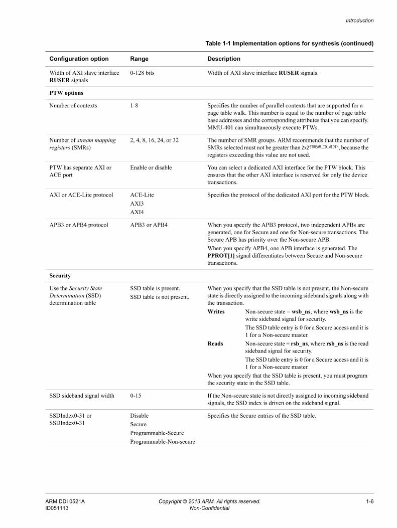
1.3 Implementation options for synthesisTable 1-1 shows the implementation options for synthesis.
Note In this document, the term configured means statically configured, where Table 1-1 defines a set of selected configuration options.
Table 1-1 Implementation options for synthesis
Configuration option Range Description
TLB options
AXI-ACE-Lite protocol ACE-LiteAXI3AXI4
When a dedicated AXI master interface is selected for the PTW, the dedicated master can have a different AXI type from the common AXI interface. If the interface is used for the PTW, then you must use the same AXI types.DVM signaling is available when the dedicated PTW interface or the combined interface without the dedicated PTW interface is of ACE-Lite type.AXI3 does not support:• Write data interleaving.• Locked transactions.
AXI data bus width 64 or 128 Width, in bits, of the AXI data bus. This is the same for both AXI masters if a separate PTW master is selected.
AXI ID signal width 0-23 The incoming AXI ID width is configurable from 0-23. The output AXI ID width changes based on the selected AXI type. For more information, see the CoreLink MMU-401 System Memory Management Unit AMBA Designer (ADR-400) User Guide Supplement.
TLB depth 2-64 The TLB depth.
Implement the TLB using a memory
RAM is used for the TLB.RAM is not used for the TLB.
You can implement the TLB data portion as RAM or flip-flops. Implementing the data portion as RAM optimizes area, but the setup and clock-to-Q delay for the RAM is higher compared to using flip-flops.
Depth of the write buffer 0, 4, 8, or 16 The write buffer can accommodate multiple bursts up to the depth of the buffer. The write data path is not stalled for transactions that the write buffer can hold. For more information, see Hit-Under-Miss on page 2-9.
StreamID - width of the sideband signal
1-15 The width of the StreamID. For more information, see Stream ID on page 2-7.
Width of AXI slave interface AWUSER signals
0-128 bits Width of AXI slave interface AWUSER signals.
Width of AXI slave interface WUSER signals
0-128 bits Width of AXI slave interface WUSER signals.
Width of AXI slave interface BUSER signals
0-128 bits Width of AXI slave interface BUSER signals.
Width of AXI slave interface ARUSER signals
0-128 bits Width of AXI slave interface ARUSER signals.
ARM DDI 0521A Copyright © 2013 ARM. All rights reserved. 1-5ID051113 Non-Confidential
Introduction
Width of AXI slave interface RUSER signals
0-128 bits Width of AXI slave interface RUSER signals.
PTW options
Number of contexts 1-8 Specifies the number of parallel contexts that are supported for a page table walk. This number is equal to the number of page table base addresses and the corresponding attributes that you can specify. MMU-401 can simultaneously execute PTWs.
Number of stream mapping registers (SMRs)
2, 4, 8, 16, 24, or 32 The number of SMR groups. ARM recommends that the number of SMRs selected must not be greater than 2x2STREAM_ID_WIDTH, because the registers exceeding this value are not used.
PTW has separate AXI or ACE port
Enable or disable You can select a dedicated AXI interface for the PTW block. This ensures that the other AXI interface is reserved for only the device transactions.
AXI or ACE-Lite protocol ACE-LiteAXI3AXI4
Specifies the protocol of the dedicated AXI port for the PTW block.
APB3 or APB4 protocol APB3 or APB4 When you specify the APB3 protocol, two independent APBs are generated, one for Secure and one for Non-secure transactions. The Secure APB has priority over the Non-secure APB.When you specify APB4, one APB interface is generated. The PPROT[1] signal differentiates between Secure and Non-secure transactions.
Security
Use the Security State Determination (SSD) determination table
SSD table is present.SSD table is not present.
When you specify that the SSD table is not present, the Non-secure state is directly assigned to the incoming sideband signals along with the transaction.Writes Non-secure state = wsb_ns, where wsb_ns is the
write sideband signal for security.The SSD table entry is 0 for a Secure access and it is 1 for a Non-secure master.
Reads Non-secure state = rsb_ns, where rsb_ns is the read sideband signal for security.The SSD table entry is 0 for a Secure access and it is 1 for a Non-secure master.
When you specify that the SSD table is present, you must program the security state in the SSD table.
SSD sideband signal width 0-15 If the Non-secure state is not directly assigned to incoming sideband signals, the SSD index is driven on the sideband signal.
SSDIndex0-31 or SSDIndex0-31
DisableSecureProgrammable-SecureProgrammable-Non-secure
Specifies the Secure entries of the SSD table.
Table 1-1 Implementation options for synthesis (continued)
Configuration option Range Description
ARM DDI 0521A Copyright © 2013 ARM. All rights reserved. 1-6ID051113 Non-Confidential

Introduction
Registering
AWUSER slave interface registering options
ForwardReverseFullBypass
Each AXI channel has a configurable register slice in the MMU-401 slave interface. This register slice is configured to be bypass registered, fully registered, forward registered, or reverse registered. An I/O delay of 70 percent of the clock is assumed for interfaces that are driven to or driven by a register.An I/O delay of 40 percent of the clock is assumed for interfaces that are bypassed.
WUSER slave interface registering options
BUSER slave interface registering options
ARUSER slave interface registering options
RUSER slave interface registering options
Register the bus between PTW and TLB blocks
ForwardReverseFull Bypass
Register slice for PTW request and acknowledge bus.A register slice on the bus that carries PTW request and acknowledge information. This can help if the routing delay between the TLB and the PTW logic is high.Register the bus between TLB
and PTW blocks
Table 1-1 Implementation options for synthesis (continued)
Configuration option Range Description
ARM DDI 0521A Copyright © 2013 ARM. All rights reserved. 1-7ID051113 Non-Confidential

Introduction
1.4 Product revisionsThis section describes the differences in functionality between product revisions of the MMU-401:
r0p0 First release.
ARM DDI 0521A Copyright © 2013 ARM. All rights reserved. 1-8ID051113 Non-Confidential

Chapter 2 Functional Description
This section describes the functional operation of the MMU-401, described in the following sections: • Interfaces on page 2-2.• Stream ID on page 2-7.• Security determination on page 2-8.• Hit-Under-Miss on page 2-9.• Fault handling on page 2-10.• Dynamic programming on page 2-11.
ARM DDI 0521A Copyright © 2013 ARM. All rights reserved. 2-1ID051113 Non-Confidential
Functional Description
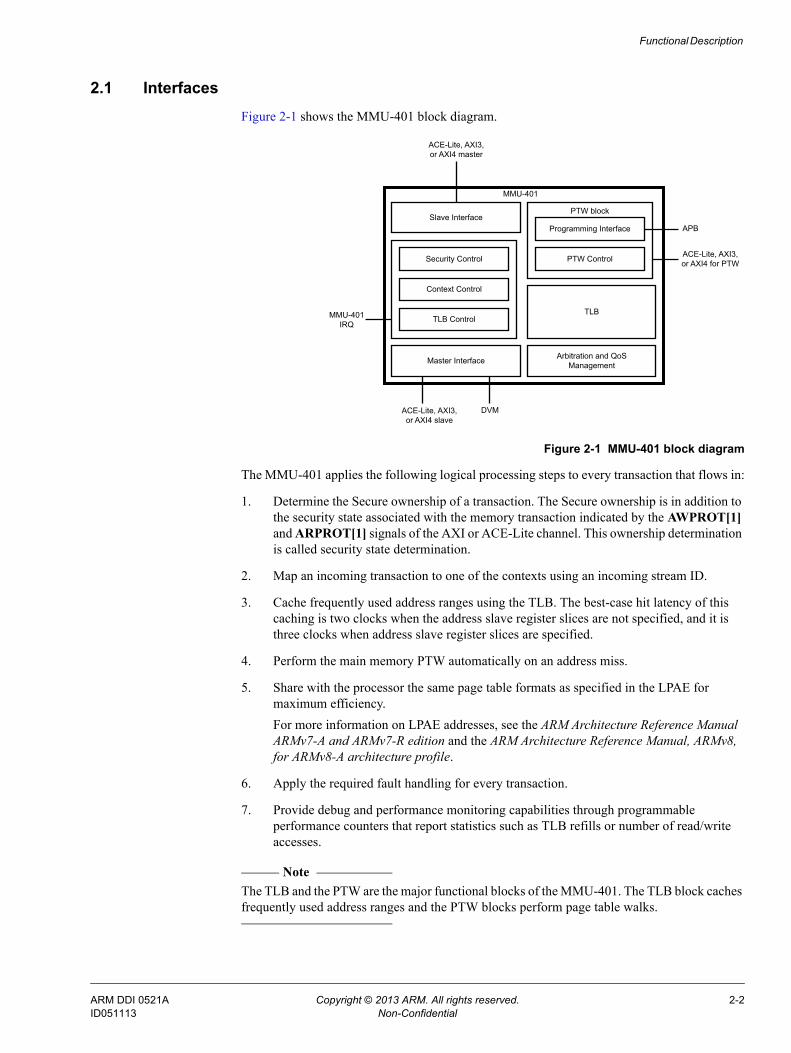
2.1 InterfacesFigure 2-1 shows the MMU-401 block diagram.
Figure 2-1 MMU-401 block diagram
The MMU-401 applies the following logical processing steps to every transaction that flows in:
1. Determine the Secure ownership of a transaction. The Secure ownership is in addition to the security state associated with the memory transaction indicated by the AWPROT[1] and ARPROT[1] signals of the AXI or ACE-Lite channel. This ownership determination is called security state determination.
2. Map an incoming transaction to one of the contexts using an incoming stream ID.
3. Cache frequently used address ranges using the TLB. The best-case hit latency of this caching is two clocks when the address slave register slices are not specified, and it is three clocks when address slave register slices are specified.
4. Perform the main memory PTW automatically on an address miss.
5. Share with the processor the same page table formats as specified in the LPAE for maximum efficiency.For more information on LPAE addresses, see the ARM Architecture Reference Manual ARMv7-A and ARMv7-R edition and the ARM Architecture Reference Manual, ARMv8, for ARMv8-A architecture profile.
6. Apply the required fault handling for every transaction.
7. Provide debug and performance monitoring capabilities through programmable performance counters that report statistics such as TLB refills or number of read/write accesses.
Note The TLB and the PTW are the major functional blocks of the MMU-401. The TLB block caches frequently used address ranges and the PTW blocks perform page table walks.
Slave InterfaceProgramming Interface
Security Control
Context Control
TLB Control
Master Interface
TLB
Arbitration and QoS Management
APB
MMU-401IRQ
ACE-Lite, AXI3, or AXI4 slave
DVM
PTW Control
PTW block
ACE-Lite, AXI3, or AXI4 master
ACE-Lite, AXI3, or AXI4 for PTW
MMU-401
ARM DDI 0521A Copyright © 2013 ARM. All rights reserved. 2-2ID051113 Non-Confidential

Functional Description
The AXI master interface, with _m suffix, drives the translated address to a downstream slave. You must connect pin-to-pin the read address channel, the write address channel, the read data channel, the write data channel, and the buffered write response channel to the corresponding AXI slave interface.
If the MMU-401 is configured to support a dedicated interface for page table walks, then you must connect the read address channel and the read data response channel of the slave interface responsible for the page table walks to the page table walk channel of the MMU-401. In this configuration, the channel that performs the page table walk contains the _ptw suffix. For example, araddr_ptw and acaddr_ptw.
You must connect pin-to-pin the read address channel, the write address channel, the read data channel, the write data channel, and the buffered write response channel of the AXI slave interface, with _s suffix to the corresponding AXI master interface. In a system, the master interface can be the AXI bus infrastructure output or an output of a bridge that converts another bus protocol to AXI.
There must be AXI type compatibility between the MMU-401 and the master connected to the MMU-401.
he MMU-401 contains the following interfaces: • Programming interface.• AXI3, AXI4, or ACE-Lite interface on page 2-4.• Low-power interface and clock gating on page 2-5.
2.1.1 Programming interface
To enable the software to program the registers of MMU-401 and to perform debug operations in the MMU-401, use the APB interface as the programming interface.
The MMU-401 provides one of the following APB programming interfaces, which is selected during the MMU-401 configuration:
• The APB4 programming interface. For more information on integrating the MMU-401 into AMBA 4 systems, see the AMBA Specification.
• Two APB3 programming interfaces. One of the APB interfaces is configured as Secure, and other interface is configured as Non-secure. You must ensure that only Secure transactions are sent on the Secure interface and only Non-secure transactions on the Non-secure interface. For more information, see the AMBA 3 APB Protocol Specification.
The programming interface also contains the APB slave interface, as the following section describes:
• APB slave interface.
APB slave interface
You must connect the APB slave interface to an AMBA 3 APB or AMBA 4 APB master based on the APB configuration type.
If you have configured the AMBA 3 APB interface, then there are two ports with _s suffix for Secure register accesses and _ns suffix for Non-secure register accesses.
The MMU-401 provides a 32-bit address bus, paddr[31:0], but it only uses bits[15:2]. The MMU-401 ignores:
• Bits[31:16], but their presence facilitates the process of integrating the MMU-401 with adjacent RTL blocks, such as an interconnect.
ARM DDI 0521A Copyright © 2013 ARM. All rights reserved. 2-3ID051113 Non-Confidential

Functional Description
• Bits[1:0] because the MMU-401 only permits word accesses to its internal registers.
If the APB interface is not running at the same frequency as that of the cclk signal, then you can divide down the frequency using the value of the pclken signal.
When operating at this frequency, the APB master must also use the pclken signal so that signal states change only on enabled clock edges. If the APB interface is to run at the same frequency as that of the cclk signal, then ensure that the pclken signal is tied high.
2.1.2 AXI3, AXI4, or ACE-Lite interface
You can configure the MMU-401 to use the AXI3, AXI4, or ACE-Lite interface to receive transactions, translate transactions, and perform page table walks. The interface information is described in the following sections:• AXI3 interface.• AXI4 interface.• ACE-Lite interface.• TLB block barrier support on page 2-5.
AXI3 interface
The MMU-401 supports the AXI3 protocol when configured to do so. In this mode, only the AXI3 signaling is present on the main data path through the MMU-401.
The MMU-401 supports DVM messages only if a dedicated ACE-Lite master port is configured for the PTW block.
The following features of AXI3 are not supported in the MMU-401:• Write data interleaving.
Note Data corruption can occur if write data and write address ordering are not the same.
• Locked transactions. The AxLOCK[1] signal bit cannot be set to 1. However, if any transaction has its AxLOCK[1] set, then it is ignored, and the output transaction has the AxLOCK[1] reset. The other bits of the AxLOCK signal are supported.
Note If the MMU-401 receives a locked transaction, the output transaction is passed to the
downstream slave as a normal access.
AXI4 interface
The MMU-401 supports the AXI4 protocol when configured to do so. In this mode, only the AXI4 signaling is present on the main data path through the MMU-401.
The MMU-401 supports DVM messages only if a dedicated ACE-Lite master port is configured for the PTW block.
ACE-Lite interface
The MMU-401 supports the ACE-Lite protocol when configured to do so. In this mode, only the ACE-Lite signaling is present on the main data path through the MMU-401.
The MMU-401 supports DVM messages with a combined master port or when a separate ACE-Lite master port is configured for the PTW block.
ARM DDI 0521A Copyright © 2013 ARM. All rights reserved. 2-4ID051113 Non-Confidential
Functional Description
Note The MMU-401 does not support invalidation by the IPA or the ARMv8 enhanced DVM messages for invalidation by the IPA.
When you configure the MMU-401 to support ACE-Lite, you must connect the AC channel of the MMU-401 to one of the following: • The AC channel driven by the CCI.• An ACE compatible slave interface that supports DVM messages.
ARM recommends you use the DVM channel for TLB maintenance operations. If the system cannot connect to this channel, you must tie the ACVALID signal low and you can use the programming interface for TLB maintenance operations.
When you configure the MMU-401 to provide a dedicated AXI channel for performing page table walks, you must specify the ACVALID channel to be a part of the channel that performs the page table walks.
TLB block barrier support
A TLB block in the MMU-401 receives and passes on barriers, but does not generates barriers of its own, in response to the SYNC signal received from the DVM channel of the PTW block.
The PTW block sends the SYNC signal to the TLB block on receiving one of the following:• A programmed SYNC message.• A DVM SYNC message that is generated by the MMU-401.
See the AMBA AXI and ACE Protocol Specification AXI3, AXI4, and AXI4-Lite ACE and ACE-Lite for more information on SYNC and DVM SYNC messages
2.1.3 Low-power interface and clock gating
The MMU-401 has two Low-Power Interfaces (LPIs) each of which must be connected pin-to-pin to a dedicated interface of a central clock controller. You can use the LPIs to disable the clock of each sub-block of the MMU-401. Alternatively, if there is no system control block, then you must tie the csysreq_* signal inputs high, and you can leave the LPI outputs, the csysack_* and cactive_* signals, unconnected.
See the AMBA AXI and ACE Protocol Specification for additional information on the function of these signals.
Note • See the AMBA AXI and ACE Protocol Specification, AXI3, AXI4, and AXI4-Lite, ACE and
ACE-Lite for the information on denial of service, that is when the following conditions are true: 1. The CACTIVE signal is high.2. The CSYSACK signal is low.
• ARM recommends that you gate the clock when the CSYSACK signal falls.
The MMU-401 has two C-channels that allow you to disable the clock for the PTW and TLB blocks independently, as the following sections describe:• TLB block on page 2-6.• PTW block on page 2-6.
ARM DDI 0521A Copyright © 2013 ARM. All rights reserved. 2-5ID051113 Non-Confidential
Functional Description
TLB block
An external clock controller can request the TLB block to enter the low-power state by de-asserting the csysreq_tbu signal.
The TLB block can enter the low-power state under the following conditions:• No outstanding accesses are pending.• No input access is pending.• No TLB maintenance operation is pending.
When the preceding conditions are met, the cactive_tbu signal is made low. The low-power entry request is acknowledged by turning the csysreq_tbu signal low. You can disable the clock when the csysack_tbu and cactive_tbu signals are low. See LPI signals on page A-18 for information on the C-channel signals.
PTW block
During normal operation, the PTW block is in the idle state. Hence, ARM recommends that you disable the clock for this block.
An external clock controller can request the PTW block to enter the low-power mode by de-asserting the csysreq_tcu signal.
The PTW block pulls the cactive_tcu signal low under the following conditions:• The PSELx signal is low.• The ACVALID signal is low.• No outstanding PTW requests are pending.
The PSELx signal is directly connected to the cactive_tcu signal. Therefore, if the APB interface is synthesized at a value less than that of the cclk signal using the pclken signal, treat the cactive_tcu signal as one of the following to prevent metastability problems in the clock controller: • Asynchronous.• Sampled with the PCLKEN signal.
The PTW block acknowledges the low-power entry request by setting the csysack_tcu signal low. You can disable the clock when the csysack_tcu and cactive_tcu signals are low. See LPI signals on page A-18 for information on C-channel signals.
ARM DDI 0521A Copyright © 2013 ARM. All rights reserved. 2-6ID051113 Non-Confidential
Functional Description
2.2 Stream IDA stream ID is used to map an incoming transaction to a context by using a stream mapping table. The characteristics of the stream ID are as follows:
• The width of the stream ID is selected during the MMU-401 configuration.
• You must specify the stream ID on a dedicated AXI sideband signal. The sideband signal width can vary from 1-15, and separate sideband signals are used for read and write transactions.
See the ARM System Memory Management Unit Architecture Specification for information on stream ID-to-context mapping.
ARM DDI 0521A Copyright © 2013 ARM. All rights reserved. 2-7ID051113 Non-Confidential
Functional Description
2.3 Security determinationThe MMU-401 determines the Secure ownership of a transaction in one of the following ways:
• The Non-secure state is directly assigned to an incoming sideband signal along with a transaction:— For write accesses, the Non-secure state is the write sideband signal for security.— For read accesses, the Non-secure state is the read sideband signal for security
• The security state of a master is determined by using the input signals that index an SSD index into the SSD index table. The entry in the SSD index table determines whether the master that initiates the transaction is Secure or Non-secure.— The width of the SSD index is configurable from 0-15 bits.— The number of programmable entries in the SSD table is configurable from 1-32.— The SSD table entries are either programmable for security state at runtime, or
non-programmable and fixed at configuration time.
After the SSD index is determined, the SSD table comprises bits from 0-2(SSD Index WIDTH)-1. You must determine the status of the bits as follows:
List of non-programmable indices For these indices, the security state of the master is defined, and does not change. You must supply the indices of the masters whose security states are always Secure.
List of programmable indices You can programme the security state of the programmable indices.You must determine the default state of each master whose security state is programmable.An SSD index might be programmable or non-programmable, and might be in Secure or Non-secure state. By default, an SSD index is in the non-programmable Non-secure state.
Note An entry must not be duplicated in more than one list.
At least one programmable or fixed Non-secure entry must be available in every configuration.
The number of indices is determined by the configured SSD index width. For example, if the SSD index width is 6 bits, there are 64 indices in the range 0-63. You must programme the indices to be one of: programmable Secure, programmable Non-secure, or non-programmable Secure. Any unprogrammed indices default to non-programmable Non-secure.
See the ARM System Memory Management Unit Architecture Specification for information on security determination.
ARM DDI 0521A Copyright © 2013 ARM. All rights reserved. 2-8ID051113 Non-Confidential

Functional Description
2.4 Hit-Under-MissHit-Under-Miss (HUM) translates a TLB miss transaction and passes the transaction to a downstream slave if the translated TLB miss transaction results in a TLB hit. HUM characteristics for read and write transactions are as follows:
• If the transactions are read accesses, HUM is automatically enabled.
• If the transactions are write operations, HUM is enabled or disabled based on the write buffer depth. You can specify the write buffer depth during configuration.
• If the depth of the write buffer is 0, HUM for write transactions is automatically disabled.
• If the depth of the write buffer is a non-zero value, a hit write transaction is translated only if the write data from a missed transaction can be accommodated in the write buffer.
• The number of outstanding missed transactions is determined by the depth of the write buffer. For example, if the depth of the buffer is four, then it can hold two transactions of length two. Each buffer entry holds only one beat of the transaction, even if it is of a narrow width.
Example 2-1 Hit under miss
If the write buffer depth is eight, and there is a missed write transaction of length four and a missed write transaction of length three, the transactions are stored in the write buffer when the page table walks for the transactions are performed. If another write hit transaction is performed, it is passed through.
Note If the write buffer is full with missed write transactions, then HUM cannot occur.
ARM DDI 0521A Copyright © 2013 ARM. All rights reserved. 2-9ID051113 Non-Confidential

Functional Description
2.5 Fault handlingThe MMU-401 only supports the terminate fault handling mode that the ARM System Memory Management Unit Architecture Specification describes. Fault stalling is not supported.
You can specify the fault reporting characteristics using the following registers: • The Secure configuration register for global faults.• The system control register of the context for context faults.
A faulted transaction is aborted (reported as a fault) depending on the values programmed in these registers.
A faulted transaction causes the next incoming transaction to fault when the following conditions are true:
• The second transaction is in the same 4KB region and is in the same context as the first transaction.
• The second transaction is received before the response for the first transaction is sent by the MMU-401.
These faults can occur even if a fault clear is received between the first and second transactions.
For more information on fault handling, see the ARM System Memory Management Unit Architecture Specification.
For more information on fault reporting, see the ARM Architecture Reference Manual ARMv7-A and ARMv7-R editions and the ARM Architecture Reference Manual, ARMv8, for ARMv8-A architecture profile.
Note If you use the APB4 programming interface, a register access results in a configuration access fault under the following conditions:• Instruction accesses that set PPROT[0] to 0.• Normal accesses that set PPROT[2] to 1.
ARM DDI 0521A Copyright © 2013 ARM. All rights reserved. 2-10ID051113 Non-Confidential

Functional Description
2.6 Dynamic programmingARM recommends that you modify the contents of a control register only when there are no outstanding transactions in the MMU-401. If any of the control registers are modified when there is an existing transaction in the MMU-401, then the following behavior occurs:
• If a transaction arrives at the MMU-401 after the PREADY signal when a control register is written, the MMU-401 ensures that the new register attributes are applied to the transaction.
• If a transaction is pending within the MMU-401 when a control register is written, it is unpredictable whether the old register attributes or the new register attributes are applied to the transaction.
ARM DDI 0521A Copyright © 2013 ARM. All rights reserved. 2-11ID051113 Non-Confidential
Chapter 3 Programmers Model
This chapter describes the MMU-401 registers and provides information about programming the MMU-401, as the following sections describe:• About the programmers model on page 3-2.• The MMU-401 address map on page 3-3.• Register summary on page 3-5.• Global register space 0 on page 3-11.• Global register space 1 on page 3-33.• Integration registers on page 3-36.• Performance monitoring registers on page 3-39.• Security state determination address space on page 3-46.• Peripheral and component identification registers on page 3-48.• Translation context-bank registers on page 3-52.
ARM DDI 0521A Copyright © 2013 ARM. All rights reserved. 3-1ID051113 Non-Confidential

Programmers Model
3.1 About the programmers modelThe following information applies to the MMU-401 registers:
• Registers are implemented according to the ARM System Memory Management Unit Architecture Specification with the security extensions implemented in the MMU-401 as follows:— Global space 0 registers summary on page 3-5.— Global space 1 register summary on page 3-7.— Integration registers summary on page 3-7.— Performance monitoring registers summary on page 3-8.— The MMU-401 security state determination address space summary on page 3-8.— Peripheral and component identification summary on page 3-9.— Translation context-bank address map summary on page 3-9.
The following information applies to the MMU-401 registers:
• Unless otherwise stated in the accompanying text:— Do not modify undefined register bits.— Ignore undefined register bits on reads.— All register values are UNKNOWN on reset unless otherwise stated.
• Access types of the MMU-401 registers are described as follows:RAO Read-As-One.RAO/SBOP Read-As-One, Should-Be-One-or-Preserved on writes.RAO/WI Read-As-One, Writes Ignored.RAZ Read-As-Zero.RAZ/SBZP Read-As-Zero, Should-Be-Zero-or-Preserved on writes.RAZ/WI Read-As-Zero, Writes Ignored.RO Read-only.RW Read and write.SBO Should-Be-One.SBOP Should-Be-One-or-Preserved.SBZ Should-Be-Zero.SBZP Should-Be-Zero-or-Preserved.UNK Unknown.WI Write-ignored.WO Write-only.
• When you configure registers using the APB4 programming interface, all transactions must be privileged access and data. In other words, you must set PPROT[0]=1 and PPROT[2]=0, else the transactions are treated as RAZ/WI.
ARM DDI 0521A Copyright © 2013 ARM. All rights reserved. 3-2ID051113 Non-Confidential

Programmers Model
3.2 The MMU-401 address mapThe address map of the programming interface is consistent with the ARM System Memory Management Unit Architecture Specification.
In addition to the registers specified in the ARM System Memory Management Unit Architecture Specification, the MMU-401 implements the following configuration, identification, debug, context, integration, performance, and control registers:• Secure configuration register 0, SMMU_SCR0.• Auxiliary configuration register, SMMU_SACR.• Identification registers:
— Identification register 0.— Identification register 1.— Identification register 2.— Identification register 7.
• Debug read pointer register, SMMU_DBGRPTR.• Debug read data register, SMMU_DBGRDATA• Secure alias to Non-secure configuration register 0.• Secure Alias to Non-secure auxiliary configuration register.• Stream match registers, SMMU_SMRn.• Stream to context registers, SMMU_S2CRn.• Context-bank fault restricted syndrome registers A, SMMU_CBFRSYNRAn.• Context-bank attribute registers, SMMU_CBARn.• Integration enable register, ITEN.• Integration test input register, ITIP.• Integration test output register, ITOP. • Performance monitor event count registers, SMMU_PMEVCNTn.• Performance monitor counter group configuration registers, PMCGCRn.• Performance monitor counter group stream match registers, PMCGSMRn.• Performance monitor configuration register, PMCFG.• Performance monitor control register, PMCR.• Performance monitor authentication status register, SMMU_CBn_AUTHSTATUS.• Performance monitor device type register, PMDEVTYPE.• Component identification registers, CIDn.• Peripheral identification registers, PIDn.
— PID0.— PID1.— PID2.— PID3.— PID4.— PID5-7.
• System Control Registers, SMMU_CBn_SCTLR.• Translation Table Base Control Registers, SMMU_CBn_TTBCR.
The MMU-401 is configured through a memory-mapped register frame. The total size of the MMU-401 address range depends on the number of implemented translation contexts.
ARM DDI 0521A Copyright © 2013 ARM. All rights reserved. 3-3ID051113 Non-Confidential

Programmers Model
The MMU-401 address map consists of the following equally-sized portions:
The global address space The global address space is located at the bottom of the MMU-401 address space, at SMMU_BASE. See Figure 3-1.
The translation context-bank address space The translation context-bank address space is located above the top of the global address space, at SMMU_TOP. See Figure 3-1.
Figure 3-1 MMU-401 address map
You can determine the MMU-401 address range by reading the following register fields: • SMMU_IDR1.PAGESIZE.• SMMU_IDR1.NUMPAGENDXB.
For more information, see the ARM System Memory Management Unit Architecture Specification.
Translation context-bank address space
Global address spaceSMMU_BASE
SMMU_TOP
SMMU_CB_BASESMMU_GLOBAL_TOP
ARM DDI 0521A Copyright © 2013 ARM. All rights reserved. 3-4ID051113 Non-Confidential
Programmers Model
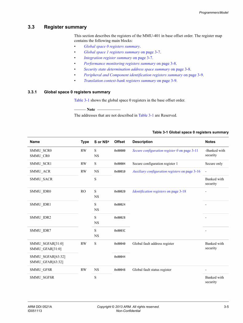
3.3 Register summaryThis section describes the registers of the MMU-401 in base offset order. The register map contains the following main blocks:• Global space 0 registers summary.• Global space 1 registers summary on page 3-7.• Integration register summary on page 3-7.• Performance monitoring registers summary on page 3-8.• Security state determination address space summary on page 3-8.• Peripheral and Component identification registers summary on page 3-9.• Translation context-bank registers summary on page 3-9.
3.3.1 Global space 0 registers summary
Table 3-1 shows the global space 0 registers in the base offset order.
Note The addresses that are not described in Table 3-1 are Reserved.
Table 3-1 Global space 0 registers summary
Name Type S or NSa Offset Description Notes
SMMU_SCR0SMMU_CR0
RW SNS
0x00000 Secure configuration register 0 on page 3-11 -Banked with security
SMMU_SCR1 RW S 0x00004 Secure configuration register 1 Secure only
SMMU_ACR RW NS 0x00010 Auxiliary configuration registers on page 3-16 -
SMMU_SACR S Banked with security
SMMU_IDR0 RO SNS
0x00020 Identification registers on page 3-18 -
SMMU_IDR1 SNS
0x00024 -
SMMU_IDR2 SNS
0x00028 -
SMMU_IDR7 SNS
0x0003C -
SMMU_SGFAR[31:0]SMMU_GFAR[31:0]
RW S 0x00040 Global fault address register Banked with security
SMMU_SGFAR[63:32]SMMU_GFAR[63:32]
0x00044
SMMU_GFSR RW NS 0x00048 Global fault status register -
SMMU_SGFSR S Banked with security
ARM DDI 0521A Copyright © 2013 ARM. All rights reserved. 3-5ID051113 Non-Confidential

Programmers Model
SMMU_GFSRRESTORE WO NS 0x0004C Global fault status register restore -
SMMU_SGFSRRESTORE S Banked with security
SMMU_GFSYNR0 RW NS 0x00050 Global fault syndrome register 0 -
SMMU_SGFSYNR0 S Banked with security
SMMU_GFSYNR1 RW NS 0x00054 Global fault syndrome register 1 -
SMMU_SGFSYNR1 S Banked with security
SMMU_STLBIALL WO SNS
0x00060 Invalidate entire TLB register -
SMMU_TLBIVMID WO NS 0x00064 Invalidate TLB by the virtual machine identifier (VMID) register
-
SMMU_TLBIALLNSNH WO NS 0x00068 Invalidate entire Non-secure Non-hyp TLB register
-
SMMU_STLBGSYNC WO SNS
0x00070 Global synchronize TLB invalidate register -
SMMU_TLBGSYNC -
SMMU_STLBGSTATUS RO SNS
0x00074 Global TLB status register Banked with security
SMMU_TLBGSTATUS -
SMMU_DBGRPTR RW S 0x00080 Debug registers on page 3-25 -
SMMU_DBGRDATA RO S 0x00084 -
SMMU_NSCR0 RW S 0x00400 Secure alias to Non-secure configuration register 0 on page 3-29
Secure only
SMMU_NSACR RW S 0x00410 Secure Alias to Non-secure auxiliary configuration register on page 3-30
Secure only
SMMU_NSGFAR[31:0]b RW S 0x00440 Secure alias for Non-secure global fault address register
Secure only, 64-bit
SMMU_NSGFAR[63:32]b RW S 0x00444 Secure alias for Non-secure global fault address register
SMMU_NSGFSRb WO S 0x00448 Secure alias for Non-secure global fault status register
Secure only
SMMU_NSGFSRRESTOREb WO S 0x0044C Secure alias for Non-secure global fault status register restore
Secure only
SMMU_NSGFSYNR0b RW S 0x00450 Secure alias for Non-secure global fault syndrome register 0
Secure only
SMMU_NSGFSYNR1b RW S 0x00454 Secure alias for Non-secure global fault syndrome register 1
Secure only
Table 3-1 Global space 0 registers summary (continued)
Name Type S or NSa Offset Description Notes
ARM DDI 0521A Copyright © 2013 ARM. All rights reserved. 3-6ID051113 Non-Confidential

Programmers Model
3.3.2 Global space 1 registers summary
Table 3-2 shows the translation context-bank address map in the base offset order.
3.3.3 Integration register summary
Table 3-3 shows the integration registers in the base offset order.
SMMU_NSTLBGSYNCb WO S 0x00470 Secure alias for Non-secure global synchronize TLB invalidate register
Secure only
SMMU_NSTLBGSTATUSb RO S 0x00474 Secure alias for Non-secure global TLB status register
Secure only
SMMU_SMRn RW SNS
0x00800-
0x0087C
Stream match registers on page 3-30 -
SMMU_S2CRn RW SNS
0x00C00-0x00C7C
Stream to context registers on page 3-31 -
a. S stands for Secure and NS stands for Non-secure. b. Using Secure aliases, the Non-secure version of the banked registers are accessed.
Table 3-1 Global space 0 registers summary (continued)
Name Type S or NSa Offset Description Notes
Table 3-2 Global space 1 register summary
Name Type S or NS Offset Description
SMMU_CBAR0-7 RW NS 0x1000-0x101C Context-bank attribute registers on page 3-33
SMMU_CBFRSYNRA0-7 RW 0x1400-0x141C Context-bank fault restricted syndrome registers A on page 3-34
SMMU_CBA2R0-7 RW 0x1800-0x180C See the ARM System Memory Management Unit Architecture Specification 64KB Translation Granule Supplement.
Table 3-3 Integration registers summary
Name Type S or NS Offset Description
ITEN RW NSS
0x2000 Integration enable register on page 3-36
ITIP RO 0x2004 Integration test input register on page 3-37
ITOP RW 0x2008 Integration test output register on page 3-37
ARM DDI 0521A Copyright © 2013 ARM. All rights reserved. 3-7ID051113 Non-Confidential
Programmers Model
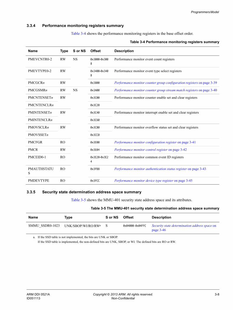
3.3.4 Performance monitoring registers summary
Table 3-4 shows the performance monitoring registers in the base offset order.
3.3.5 Security state determination address space summary
Table 3-5 shows the MMU-401 security state address space and its attributes.
Table 3-4 Performance monitoring registers summary
Name Type S or NS Offset Description
PMEVCNTR0-2 RW NS 0x3000-0x3008
Performance monitor event count registers
PMEVTYPE0-2 RW 0x3400-0x3408
Performance monitor event type select registers
PMCGCRn RW 0x3800 Performance monitor counter group configuration registers on page 3-39
PMCGSMRn RW NS 0x3A00 Performance monitor counter group stream match registers on page 3-40
PMCNTENSETn RW 0x3C00 Performance monitor counter enable set and clear registers
PMCNTENCLRn 0x3C20
PMINTENSETn RW 0x3C40 Performance monitor interrupt enable set and clear registers
PMINTENCLRn 0x3C60
PMOVSCLRn RW 0x3C80 Performance monitor overflow status set and clear registers
PMOVSSETn 0x3CC0
PMCFGR RO 0x3E00 Performance monitor configuration register on page 3-41
PMCR RW 0x3E04 Performance monitor control register on page 3-42
PMCEID0-1 RO 0x3E20-0x3E24
Performance monitor common event ID registers
PMAUTHSTATUS
RO 0x3FB8 Performance monitor authentication status register on page 3-43
PMDEVTYPE RO 0x3FCC Performance monitor device type register on page 3-45
Table 3-5 The MMU-401 security state determination address space summary
Name Type S or NS Offset Description
SMMU_SSDR0-1023 UNK/SBOP/WI/RO/RWa S 0x04000-0x04FFC Security state determination address space on page 3-46
a. If the SSD table is not implemented, the bits are UNK or SBOP. If the SSD table is implemented, the non-defined bits are UNK, SBOP, or WI. The defined bits are RO or RW.
ARM DDI 0521A Copyright © 2013 ARM. All rights reserved. 3-8ID051113 Non-Confidential

Programmers Model
3.3.6 Peripheral and Component identification registers summary
Table 3-6 shows the Peripheral and Component identification registers in the base offset order.
3.3.7 Translation context-bank registers summary
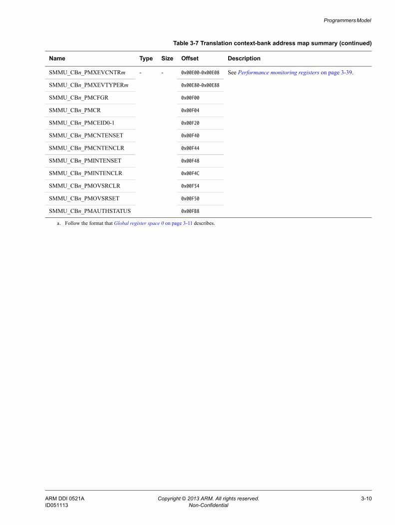
Table 3-7 shows the translation context-bank address map in the base offset order.
Table 3-6 Peripheral and component identification summary
Name Type S or NS Offset Description
Periph ID 4 RO NSS
0x0FFD0 Peripheral identification registers on page 3-48
Periph ID 5 0x0FFD4
Periph ID 6 0x0FFD8
Periph ID 7 0x0FFDC
Periph ID 0 0x0FFE0
Periph ID 1 0x0FFE4
Periph ID 2 0x0FFE8
Periph ID 3 0x0FFEC
Component ID0 0x0FFF0 Component identification registers on page 3-48
Component ID1 0x0FFF4
Component ID2 0x0FFF8
Component ID3 0x0FFFC
Table 3-7 Translation context-bank address map summary
Name Type Size Offset Description
SMMU_CBn_SCTLR RW 32 0x00000 System control register on page 3-52
SMMU_CBn_TTBR0[64:0] 64 0x00020-0x00024 Translation Table Base Register
SMMU_CBn_TTBCR 32 0x00030 Translation table base control register on page 3-55
SMMU_CBn_FSRa - - 0x00058 Fault registers: • Fault status register.• Fault status restore register.• Fault address register.• Fault syndrome registers.See the ARM System Memory Management Unit Architecture Specification.
SMMU_CBn_FSRRESTOREa 0x0005C
SMMU_CBn_FAR[31:0]a 0x00060
SMMU_CBn_FAR[63:32]a 0x00064
SMMU_CBn_FSYNR0a 0x00068
ARM DDI 0521A Copyright © 2013 ARM. All rights reserved. 3-9ID051113 Non-Confidential
Programmers Model
SMMU_CBn_PMXEVCNTRm - - 0x00E00-0x00E08 See Performance monitoring registers on page 3-39.
SMMU_CBn_PMXEVTYPERm 0x00E80-0x00E88
SMMU_CBn_PMCFGR 0x00F00
SMMU_CBn_PMCR 0x00F04
SMMU_CBn_PMCEID0-1 0x00F20
SMMU_CBn_PMCNTENSET 0x00F40
SMMU_CBn_PMCNTENCLR 0x00F44
SMMU_CBn_PMINTENSET 0x00F48
SMMU_CBn_PMINTENCLR 0x00F4C
SMMU_CBn_PMOVSRCLR 0x00F54
SMMU_CBn_PMOVSRSET 0x00F50
SMMU_CBn_PMAUTHSTATUS 0x00FB8
a. Follow the format that Global register space 0 on page 3-11 describes.
Table 3-7 Translation context-bank address map summary (continued)
Name Type Size Offset Description
ARM DDI 0521A Copyright © 2013 ARM. All rights reserved. 3-10ID051113 Non-Confidential
Programmers Model
3.4 Global register space 0The MMU-401 global register space 0 provides the high-level control of the MMU-401 resources and maps device transactions to translation context-banks, as the following sections describe:• Secure configuration register 0.• Auxiliary configuration registers on page 3-16.• Identification registers on page 3-18.• Debug registers on page 3-25.• Secure alias to Non-secure configuration register 0 on page 3-29.• Secure Alias to Non-secure auxiliary configuration register on page 3-30.• Stream match registers on page 3-30.• Stream to context registers on page 3-31.
3.4.1 Secure configuration register 0
The Secure configuration register 0, SMMU_SCR0, characteristics are:
Purpose Contains top-level control of the MMU-401 that is only accessible by a Secure access.
Note The Non-secure register, SMMU_CR0, does not provide the complete
top-level control of the MMU-401 for Secure transactions. In implementations that support security extensions, certain SMMU_CR0 fields apply only to Non-secure transactions.
Configuration Available in all configurations of the MMU-401.
Usage constraints There are no usage constraints.
Attributes See Table 3-1 on page 3-5.
Figure 3-2 on page 3-12 shows the bit assignments.
ARM DDI 0521A Copyright © 2013 ARM. All rights reserved. 3-11ID051113 Non-Confidential

Programmers Model
Figure 3-2 Secure configuration register 0 bit assignments
Table 3-8 shows the bit assignments.
31 012345678
Reserved
3029 28 27 26 25 2423 22 21 20 19 1615 13 12 11 10 9
NSCFGWACFGRACFGSHCFG
SMCFCFGMTCFG
BSUFB
PTMVMIDPNE
GSESTALLD
ReservedGFIE
GFRECLIENTPD
GCFGFREGCFGFIEReserved
14
USFCFG
MemAttr
Table 3-8 Secure configuration register 0 bit assignments
Bits Name Reset value Description
[31:30] Reserved - Reserved.
[29:28] NSCFG - Non-secure configuration. The possible values of this field are:0b00 Use the value of the APROT[1] signal that is presented with the
transaction.0b01 Reserved.0b10 Secure.0b11 Non-secure.
Note • This bit field is only present in the SMMU_SCR0 register. In the SMMU_CR0
register, the bit field is Reserved.• This bit field applies to the processing of Secure transactions that bypass the
MMU-401 stream mapping process. This bypass condition can occur if:— The SMMU_SCR0.CLIENTPD bit is set to 0b1.— The transaction does not match have a match the stream mapping table and
the SMMU_SCR0.USFCFG bit is set to 0b0.
ARM DDI 0521A Copyright © 2013 ARM. All rights reserved. 3-12ID051113 Non-Confidential

Programmers Model
[27:26] WACFG - Write allocate configuration. This bit field controls the allocation hint for write accesses. The possible values of this bit field are:0b00 Use allocation attributes that are presented with the transaction.0b01 Reserved.0b10 Allocate.0b11 No allocate.
Note This field applies to transactions that bypass the MMU-401 stream mapping table. The bypass condition can occur if: • The SMMU_CR0.CLIENTPD bit is set to 0b1.• The transaction does not have a match in the stream mapping table, and the
SMMU_CR0.USFCFG bit is set to 0b0.
[25:24] RACFG - Read allocate configuration. This bit field controls the allocation hint for read accesses. The possible values of this field are:0b00 Use allocation attributes that are presented with the transaction.0b01 Reserved.0b10 Allocate.0b11 No allocate.
Note This field applies to transactions that bypass the MMU-401 stream mapping process. This bypass condition can occur if: • The SMMU_CR0.CLIENTPD bit is set to 0b1.• The transaction does not have a match in the stream mapping table, and the
SMMU_CR0.USFCFG bit is set to 0b0.
[23:22] SHCFG - Shared configuration. The possible values of this bit field are:0b00 Use shareable attributes that are presented with the transaction.0b01 Outer-shareable.0b10 Inner-shareable.0b11 Non-shareable.
Note This field applies to transactions that bypass the MMU-401 stream mapping process. This bypass condition can occur if: • The SMMU_CR0.CLIENTPD bit is set to 0b1.• The transaction does not have a match in the stream mapping table, and the
SMMU_CR0.USFCFG bit is set to 0b0.
Table 3-8 Secure configuration register 0 bit assignments (continued)
Bits Name Reset value Description
ARM DDI 0521A Copyright © 2013 ARM. All rights reserved. 3-13ID051113 Non-Confidential

Programmers Model
[21] SMCFCFG - Stream match conflict fault configuration. This bit field controls the handling of client transactions that match multiple entries in the stream mapping table. The possible values of this bit are:0b0 Permit pass through.0b1 Raise a stream match conflict fault.
Note • The MMU-401 considers this bit as RAO/WI.• The MMU-401 does not guarantee detection of all occurrences of the stream match
conflict fault. See the ARM System Memory Management Unit Architecture Specification for more information.
[20] MTCFG 0b0 Memory type configuration. The possible values of this bit are:0b0 Use the memory attributes that are presented with the transaction. 0b1 Use the SMMU_CR0.MemAttr field for the memory attributes.
Note This field applies to the processing of Non-secure transactions that bypass the MMU-401 stream mapping process. This bypass condition can occur if: • The SMMU_CR0.CLIENTPD bit is set to 0b1.• The transaction does not have a match in the stream mapping table and the
SMMU_CR0.USFCFG bit is set to 0b0.
[19:16] MemAttr - Memory attributes. The memory attributes might be overlaid if the SMMU_CR0.MTCFG bit is set to 0b1.
[15:14] BSU - Barrier shareability upgrade. This bit upgrades the required shareability domain of the barriers issued by the client devices that are not mapped to a translation context, by setting the minimum shareability domain that is applied to a barrier. The possible values of this field are:0b00 No effect.0b01 Inner shareable.0b10 Outer shareable.0b11 Full system.
Note • The MMU-401 supports this bit only in ACE-Lite configurations.• This field only applies to barriers that are received by the MMU-401.
Table 3-8 Secure configuration register 0 bit assignments (continued)
Bits Name Reset value Description
ARM DDI 0521A Copyright © 2013 ARM. All rights reserved. 3-14ID051113 Non-Confidential
Programmers Model
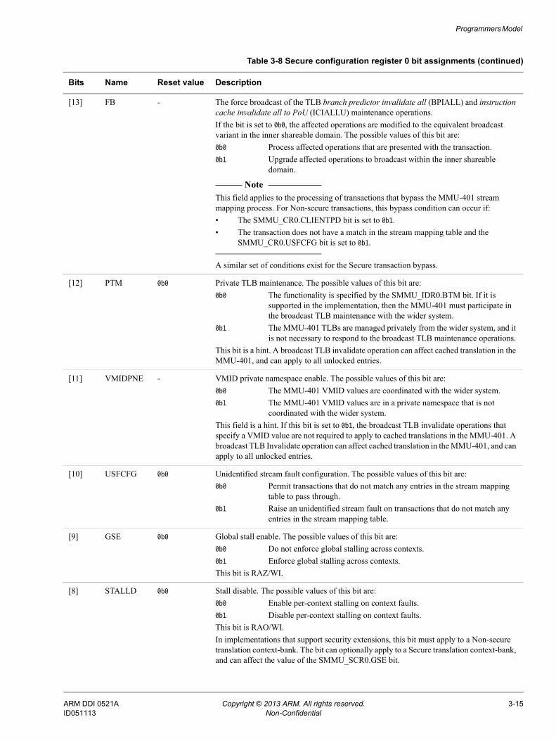
[13] FB - The force broadcast of the TLB branch predictor invalidate all (BPIALL) and instruction cache invalidate all to PoU (ICIALLU) maintenance operations. If the bit is set to 0b0, the affected operations are modified to the equivalent broadcast variant in the inner shareable domain. The possible values of this bit are:0b0 Process affected operations that are presented with the transaction.0b1 Upgrade affected operations to broadcast within the inner shareable
domain.
Note This field applies to the processing of transactions that bypass the MMU-401 stream mapping process. For Non-secure transactions, this bypass condition can occur if:• The SMMU_CR0.CLIENTPD bit is set to 0b1.• The transaction does not have a match in the stream mapping table and the
SMMU_CR0.USFCFG bit is set to 0b1.
A similar set of conditions exist for the Secure transaction bypass.
[12] PTM 0b0 Private TLB maintenance. The possible values of this bit are:0b0 The functionality is specified by the SMMU_IDR0.BTM bit. If it is
supported in the implementation, then the MMU-401 must participate in the broadcast TLB maintenance with the wider system.
0b1 The MMU-401 TLBs are managed privately from the wider system, and it is not necessary to respond to the broadcast TLB maintenance operations.
This bit is a hint. A broadcast TLB invalidate operation can affect cached translation in the MMU-401, and can apply to all unlocked entries.
[11] VMIDPNE - VMID private namespace enable. The possible values of this bit are:0b0 The MMU-401 VMID values are coordinated with the wider system.0b1 The MMU-401 VMID values are in a private namespace that is not
coordinated with the wider system.This field is a hint. If this bit is set to 0b1, the broadcast TLB invalidate operations that specify a VMID value are not required to apply to cached translations in the MMU-401. A broadcast TLB Invalidate operation can affect cached translation in the MMU-401, and can apply to all unlocked entries.
[10] USFCFG 0b0 Unidentified stream fault configuration. The possible values of this bit are:0b0 Permit transactions that do not match any entries in the stream mapping
table to pass through. 0b1 Raise an unidentified stream fault on transactions that do not match any
entries in the stream mapping table.
[9] GSE 0b0 Global stall enable. The possible values of this bit are:0b0 Do not enforce global stalling across contexts.0b1 Enforce global stalling across contexts.This bit is RAZ/WI.
[8] STALLD 0b0 Stall disable. The possible values of this bit are:0b0 Enable per-context stalling on context faults.0b1 Disable per-context stalling on context faults.This bit is RAO/WI.In implementations that support security extensions, this bit must apply to a Non-secure translation context-bank. The bit can optionally apply to a Secure translation context-bank, and can affect the value of the SMMU_SCR0.GSE bit.
Table 3-8 Secure configuration register 0 bit assignments (continued)
Bits Name Reset value Description
ARM DDI 0521A Copyright © 2013 ARM. All rights reserved. 3-15ID051113 Non-Confidential

Programmers Model
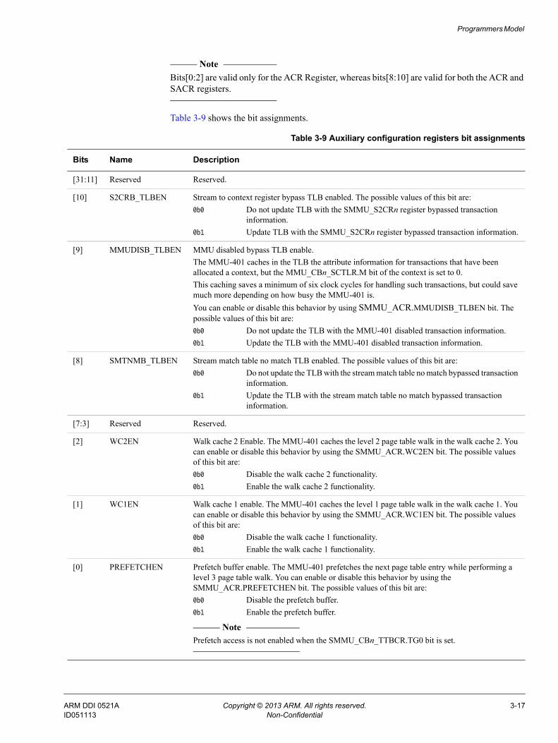
3.4.2 Auxiliary configuration registers
The auxiliary configuration registers characteristics are:
Purpose For the MMU-401, the auxiliary configuration registers, SMMU_ACR and SMMU_SACR, are defined as Table 3-9 on page 3-17 shows.
Configuration Available in all configurations of the MMU-401.
Usage constraints The WC2EN, WC1EN, and PREFETCHEN bits are Non-secure only. Other bits are banked with security.
Attributes See Global space 0 registers summary on page 3-5.
Figure 3-3 shows the bit assignments.
Figure 3-3 Auxiliary configuration registers bit assignments
[7:6] Reserved - Reserved.
[5] GCFGFIE 0b0 Global configuration fault interrupt enable. The possible values of this bit are:0b0 Do not raise an interrupt on a global configuration fault.0b1 Raise an interrupt on a global configuration fault.
[4] GCFGFRE 0b0 Global configuration fault report enable. The possible values of this bit are:0b0 Do not return an abort on a global configuration fault. 0b1 Return an abort on a global configuration fault.
[3] Reserved - Reserved.
[2] GFIE 0b0 Global fault interrupt enable. The possible values of this bit are:0b0 Do not raise an interrupt on global fault. 0b1 Raise an interrupt on a global fault.
[1] GFRE 0b0 Global fault report enable. The possible values of this bit are:0b0 Do not return an abort on a global fault. 0b1 Return an abort on a global fault.
[0] CLIENTPD 0b1 Client port disable. The possible values of this bit are:0b0 The MMU-401 client accesses are subject to translation, access control,
and attribute generation. 0b1 The MMU-401 client accesses bypass translation, access control, and
attribute generation.
Table 3-8 Secure configuration register 0 bit assignments (continued)
Bits Name Reset value Description
31 01237891011
S2CRB_TLBENMMUDISB_TLBENSMTNMB_TLBEN
WC2ENWC1EN
PREFETCHEN
ReservedReserved
ARM DDI 0521A Copyright © 2013 ARM. All rights reserved. 3-16ID051113 Non-Confidential
Programmers Model
Note Bits[0:2] are valid only for the ACR Register, whereas bits[8:10] are valid for both the ACR and SACR registers.
Table 3-9 shows the bit assignments.
Table 3-9 Auxiliary configuration registers bit assignments
Bits Name Description
[31:11] Reserved Reserved.
[10] S2CRB_TLBEN Stream to context register bypass TLB enabled. The possible values of this bit are:0b0 Do not update TLB with the SMMU_S2CRn register bypassed transaction
information.0b1 Update TLB with the SMMU_S2CRn register bypassed transaction information.
[9] MMUDISB_TLBEN MMU disabled bypass TLB enable.The MMU-401 caches in the TLB the attribute information for transactions that have been allocated a context, but the MMU_CBn_SCTLR.M bit of the context is set to 0.This caching saves a minimum of six clock cycles for handling such transactions, but could save much more depending on how busy the MMU-401 is.You can enable or disable this behavior by using SMMU_ACR.MMUDISB_TLBEN bit. The possible values of this bit are:0b0 Do not update the TLB with the MMU-401 disabled transaction information.0b1 Update the TLB with the MMU-401 disabled transaction information.
[8] SMTNMB_TLBEN Stream match table no match TLB enabled. The possible values of this bit are:0b0 Do not update the TLB with the stream match table no match bypassed transaction
information.0b1 Update the TLB with the stream match table no match bypassed transaction
information.
[7:3] Reserved Reserved.
[2] WC2EN Walk cache 2 Enable. The MMU-401 caches the level 2 page table walk in the walk cache 2. You can enable or disable this behavior by using the SMMU_ACR.WC2EN bit. The possible values of this bit are:0b0 Disable the walk cache 2 functionality.0b1 Enable the walk cache 2 functionality.
[1] WC1EN Walk cache 1 enable. The MMU-401 caches the level 1 page table walk in the walk cache 1. You can enable or disable this behavior by using the SMMU_ACR.WC1EN bit. The possible values of this bit are:0b0 Disable the walk cache 1 functionality.0b1 Enable the walk cache 1 functionality.
[0] PREFETCHEN Prefetch buffer enable. The MMU-401 prefetches the next page table entry while performing a level 3 page table walk. You can enable or disable this behavior by using the SMMU_ACR.PREFETCHEN bit. The possible values of this bit are:0b0 Disable the prefetch buffer.0b1 Enable the prefetch buffer.
Note Prefetch access is not enabled when the SMMU_CBn_TTBCR.TG0 bit is set.
ARM DDI 0521A Copyright © 2013 ARM. All rights reserved. 3-17ID051113 Non-Confidential

Programmers Model
3.4.3 Identification registers
The identification register characteristics are:
Purpose The identification registers, SMMU_IDRn and SMMU_SIDRn, provide information on the capability of the MMU-401. This section describes the following identification registers:• Identification register 0.• Identification register 1 on page 3-21.• Identification register 2 on page 3-23.• Identification register 7 on page 3-24.The MMU-401 allows the Secure software to reserve certain MMU-401 resources for its own use. See Identification register 0.The Non-secure versions of the SMMU_IDRn registers report the number of resources excluding the number reserved by the Secure software, that is, a number potentially lower than the number of physically-implemented resources.
Configuration Available in all configurations of the MMU-401.
Usage constraints There are no usage constraints.
Attributes Global space 0 registers summary on page 3-5.
Note The MMU-401 does not support stage 1 followed by stage 2 translations.
Identification register 0
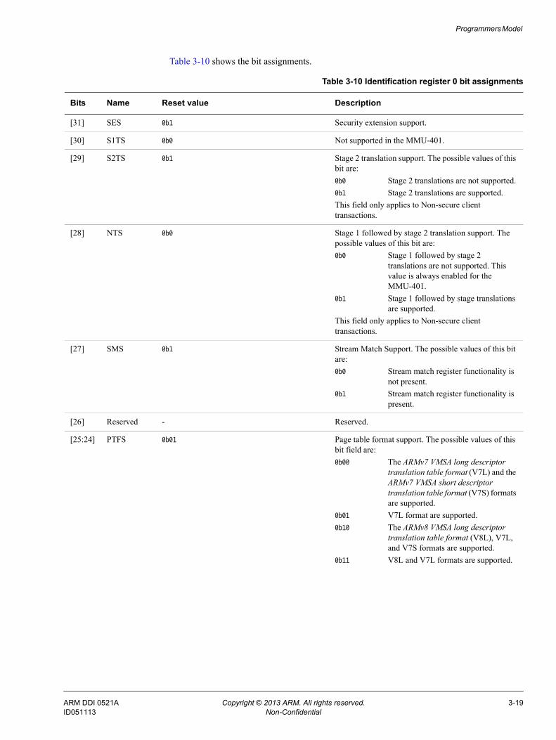
Figure 3-4 shows the bit assignments.
Figure 3-4 Identification register 0 bit assignments
31 07830 29 28 27 26 25 24 23 16 15 14 13 12 9
ReservedBTM
CTTWReserved
SMS
S1TSSES
S2TSNTS
NUMSMRGNUMSIDBNUMIRPTPTFS
ARM DDI 0521A Copyright © 2013 ARM. All rights reserved. 3-18ID051113 Non-Confidential
Programmers Model
Table 3-10 shows the bit assignments.
Table 3-10 Identification register 0 bit assignments
Bits Name Reset value Description
[31] SES 0b1 Security extension support.
[30] S1TS 0b0 Not supported in the MMU-401.
[29] S2TS 0b1 Stage 2 translation support. The possible values of this bit are:0b0 Stage 2 translations are not supported.0b1 Stage 2 translations are supported.This field only applies to Non-secure client transactions.
[28] NTS 0b0 Stage 1 followed by stage 2 translation support. The possible values of this bit are:0b0 Stage 1 followed by stage 2
translations are not supported. This value is always enabled for the MMU-401.
0b1 Stage 1 followed by stage translations are supported.
This field only applies to Non-secure client transactions.
[27] SMS 0b1 Stream Match Support. The possible values of this bit are:0b0 Stream match register functionality is
not present.0b1 Stream match register functionality is
present.
[26] Reserved - Reserved.
[25:24] PTFS 0b01 Page table format support. The possible values of this bit field are:0b00 The ARMv7 VMSA long descriptor
translation table format (V7L) and the ARMv7 VMSA short descriptor translation table format (V7S) formats are supported.
0b01 V7L format are supported.0b10 The ARMv8 VMSA long descriptor
translation table format (V8L), V7L, and V7S formats are supported.
0b11 V8L and V7L formats are supported.
ARM DDI 0521A Copyright © 2013 ARM. All rights reserved. 3-19ID051113 Non-Confidential
Programmers Model
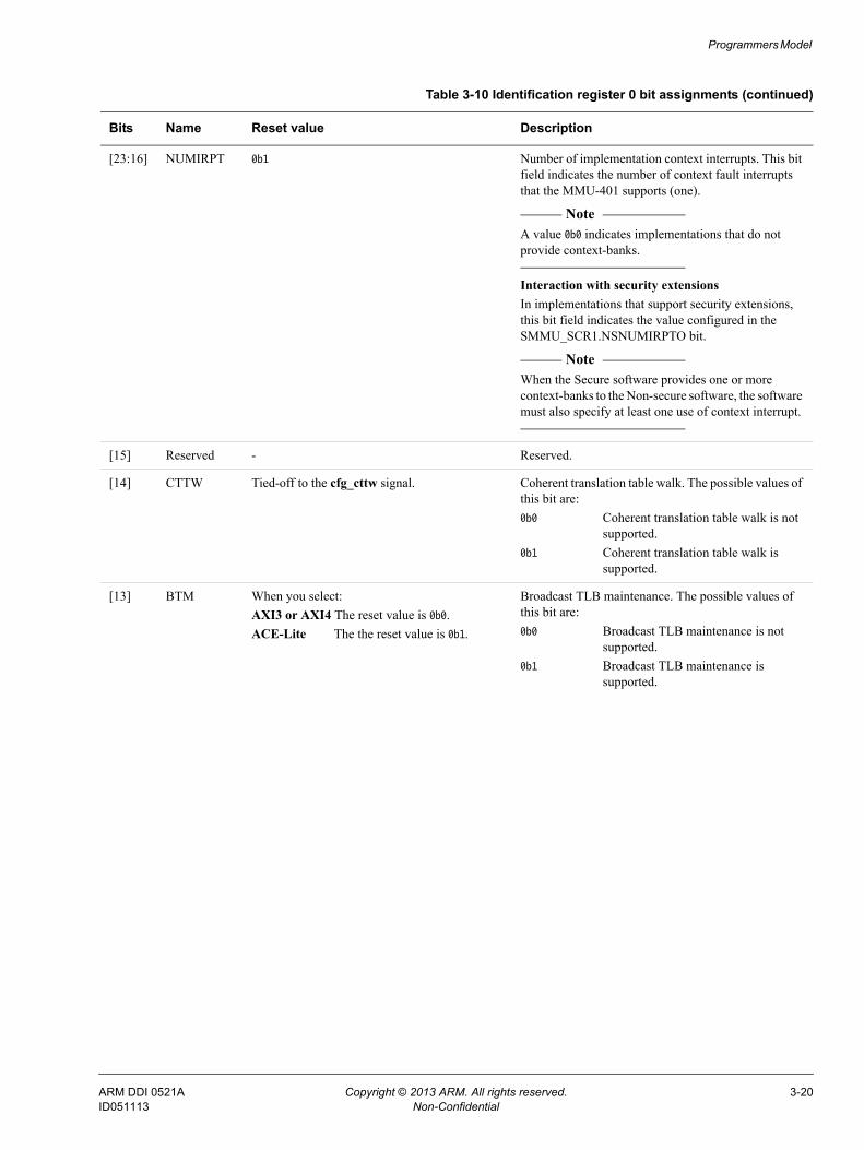
[23:16] NUMIRPT 0b1 Number of implementation context interrupts. This bit field indicates the number of context fault interrupts that the MMU-401 supports (one).
Note A value 0b0 indicates implementations that do not provide context-banks.
Interaction with security extensionsIn implementations that support security extensions, this bit field indicates the value configured in the SMMU_SCR1.NSNUMIRPTO bit.
Note When the Secure software provides one or more context-banks to the Non-secure software, the software must also specify at least one use of context interrupt.
[15] Reserved - Reserved.
[14] CTTW Tied-off to the cfg_cttw signal. Coherent translation table walk. The possible values of this bit are:0b0 Coherent translation table walk is not
supported.0b1 Coherent translation table walk is
supported.
[13] BTM When you select:AXI3 or AXI4 The reset value is 0b0.ACE-Lite The the reset value is 0b1.
Broadcast TLB maintenance. The possible values of this bit are:0b0 Broadcast TLB maintenance is not
supported.0b1 Broadcast TLB maintenance is
supported.
Table 3-10 Identification register 0 bit assignments (continued)
Bits Name Reset value Description
ARM DDI 0521A Copyright © 2013 ARM. All rights reserved. 3-20ID051113 Non-Confidential
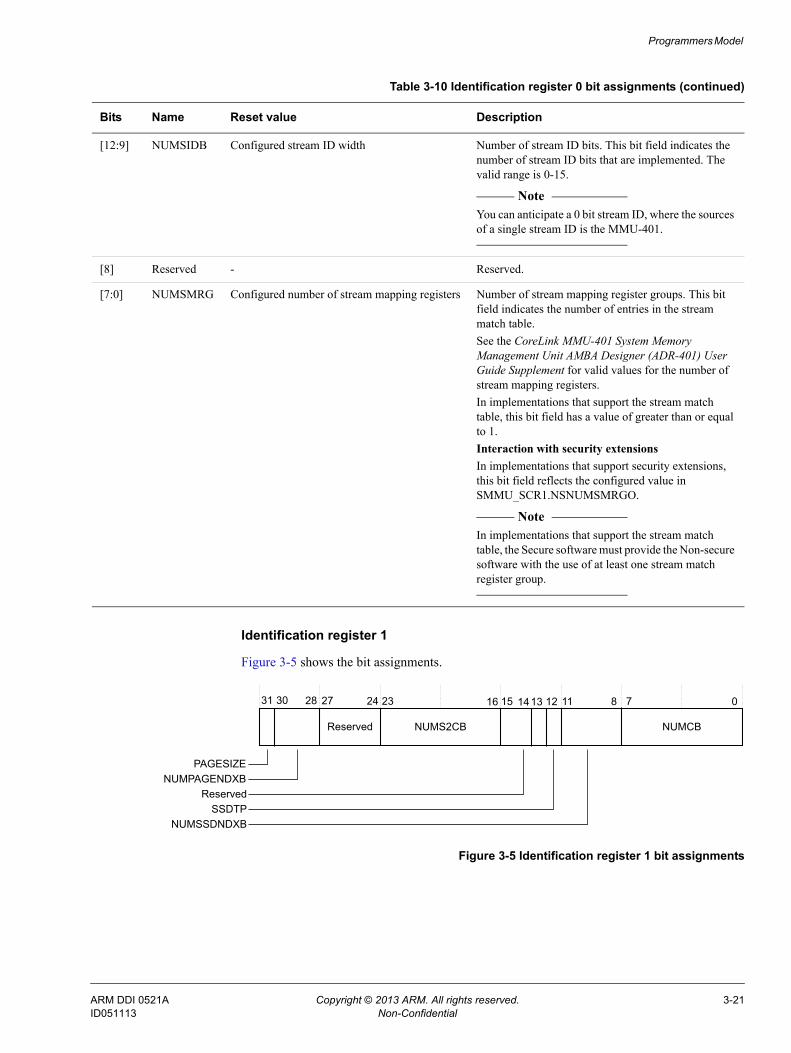
Programmers Model
Identification register 1
Figure 3-5 shows the bit assignments.
Figure 3-5 Identification register 1 bit assignments
[12:9] NUMSIDB Configured stream ID width Number of stream ID bits. This bit field indicates the number of stream ID bits that are implemented. The valid range is 0-15.
Note You can anticipate a 0 bit stream ID, where the sources of a single stream ID is the MMU-401.
[8] Reserved - Reserved.
[7:0] NUMSMRG Configured number of stream mapping registers Number of stream mapping register groups. This bit field indicates the number of entries in the stream match table.See the CoreLink MMU-401 System Memory Management Unit AMBA Designer (ADR-401) User Guide Supplement for valid values for the number of stream mapping registers.In implementations that support the stream match table, this bit field has a value of greater than or equal to 1.Interaction with security extensionsIn implementations that support security extensions, this bit field reflects the configured value in SMMU_SCR1.NSNUMSMRGO.
Note In implementations that support the stream match table, the Secure software must provide the Non-secure software with the use of at least one stream match register group.
Table 3-10 Identification register 0 bit assignments (continued)
Bits Name Reset value Description
31 07830 28 27 24 23 16 15 13 12 11
NUMSSDNDXBSSDTP
ReservedNUMPAGENDXB
PAGESIZE
14
Reserved NUMCBNUMS2CB
ARM DDI 0521A Copyright © 2013 ARM. All rights reserved. 3-21ID051113 Non-Confidential

Programmers Model
Table 3-11 shows the bit assignments.
Table 3-11 Identification register 1 bit assignments
Bits Name Reset value Description
[31] PAGESIZE 0b0 The MMU-401 page size. This bit Indicates the size of each page in the MMU-401 register map. The possible values of this bit are:0b0 4KB.0b1 64KB.
[30:28] NUMPAGENDXB 0b010 Number of page index bits. This bit indicates the number of PAGESIZE pages that occupy the global address space or the translation context address space:NUMPAGE = 2(NUMPAGENDXB+1)
[27:24] Reserved - Reserved.
[23:16] NUMS2CB Configured number of context-banks Number of stage 2 context-banks. This bit field indicates the number of context-banks that support only the stage 2 translation format. The bit field is validated by using the value of the SMMU_IDR0.S2TS bit.See the CoreLink MMU-401 System Memory Management Unit AMBA Designer (ADR-401) User Guide Supplement for information on the number of valid contexts.
[15] SMCD 0b0 Stream match conflict detection. The possible values of this bit are:0b0 Not all Stream match conflicts are
guaranteed to be detected.0b1 All Stream match conflicts are guaranteed
to be detected.See the ARM System Memory Management Unit Architecture Specification for more information.
[14:13] Reserved - Reserved.
ARM DDI 0521A Copyright © 2013 ARM. All rights reserved. 3-22ID051113 Non-Confidential

Programmers Model
Identification register 2
Figure 3-6 shows the bit assignments.
Figure 3-6 Identification register 2 bit assignments
[12] SSDTP As configured Secure status determination table is present. The possible values of this bit are:0b0 Secure status determination address space is
UNK or WI.0b1 Secure status determination address space is
populated.
Note This field is RAZ for Non-secure reads of the SMMU_IDR1 register.
[11:8] NUMSSDNDXB 4'hF Number of SSD index bits. This bit field Indicates the number of SSD index bits used to index the SSD table. This bit field is only valid if the SMMU_IDR1.SSDTP bit is high, otherwise this bit field is Reserved.
Note This field is RAZ for non-secure reads of the SMMU_IDR1 register.
[7:0] NUMCB Configured number of context-banks Number of context-banks. This bit field indicates the total number of translation context-banks that are implemented. See Translation context-bank registers on page 3-52.The value reported by this bit includes the translation context-banks that only support the stage 2 format.Interaction with security extensionsIn implementations that support security extensions, the Non-secure reads of the SMMU_IDR1 register reflect the value configured in the SMMU_SCR1.NSNUMCBO bit.
Table 3-11 Identification register 1 bit assignments (continued)
Bits Name Reset value Description
31 078 3411121314
V8MASXOS
IIPAS
15
Reserved Reserved OAS IAS
ARM DDI 0521A Copyright © 2013 ARM. All rights reserved. 3-23ID051113 Non-Confidential

Programmers Model
Table 3-12 shows the bit assignments.
Identification register 7
Figure 3-7 shows the bit assignments.
Figure 3-7 Identification register 7 bit assignments
Table 3-12 Identification register 2 bit assignments
Bits Name Reset value Description
[31:15] Reserved - Reserved.
[14] IIPAS 0b0 Invalidation of stage 2 contexts supported. The possible values of this field are:0b0 Not supported. The SMMU_CBn_TLBIIPAS2(L) registers are not supported.0b1 Supported. The SMMU_CBn_TLBIIPAS2(L) registers are supported.
Note MMU-401 does not support invalidation by the IPA and the ARMv8 enhanced DVM messages for invalidation by IPA.
[13] XOS 0b0 ARMv8 execute-only pages are supported. The possible values of this field are:0b0 Not supported. Device accesses to pages are marked as execute only trap.0b1 Supported. Device accesses to execute only pages are supported if the final
attributes of the accesses indicate an instruction. See the ARM Architecture Reference Manual, ARMv8, for ARMv8-A architecture profile.
[12] V8MAS 0b1 ARMv8 memory attributes are supported. The possible values of this field are:0b0 Supports only the ARMv7 device and strongly ordered memory attributes.0b1 Supports the ARMv8 enhanced memory attributes.
[11:5] Reserved - Reserved.
[7:4] OAS 0b0010 Output address size. The possible values of this field are:0b0000 32 bits.0b0001 36 bits.0b0010 40 bits.All other values are Reserved.
Note The MMU-401 supports only 40-bit output address size.
[3:0] IAS 0b0010 Input address size. The possible values of this field are:0b0000 32 bits.0b0001 36 bits.0b0010 40 bits.All other values are Reserved.
Note The MMU-401 supports only 40-bit input address size.
31 078 34
Reserved MAJOR MINOR
ARM DDI 0521A Copyright © 2013 ARM. All rights reserved. 3-24ID051113 Non-Confidential
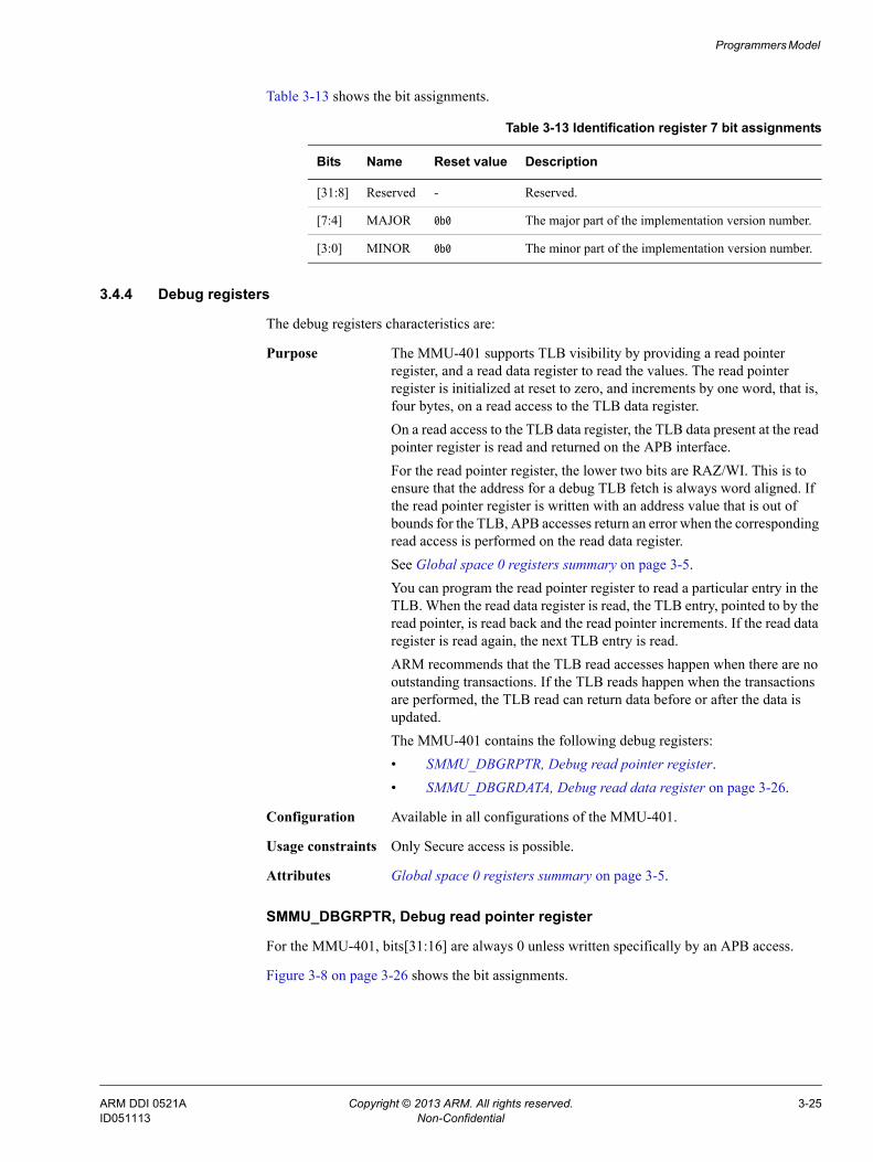
Programmers Model
Table 3-13 shows the bit assignments.
3.4.4 Debug registers
The debug registers characteristics are:
Purpose The MMU-401 supports TLB visibility by providing a read pointer register, and a read data register to read the values. The read pointer register is initialized at reset to zero, and increments by one word, that is, four bytes, on a read access to the TLB data register.On a read access to the TLB data register, the TLB data present at the read pointer register is read and returned on the APB interface. For the read pointer register, the lower two bits are RAZ/WI. This is to ensure that the address for a debug TLB fetch is always word aligned. If the read pointer register is written with an address value that is out of bounds for the TLB, APB accesses return an error when the corresponding read access is performed on the read data register. See Global space 0 registers summary on page 3-5.You can program the read pointer register to read a particular entry in the TLB. When the read data register is read, the TLB entry, pointed to by the read pointer, is read back and the read pointer increments. If the read data register is read again, the next TLB entry is read.ARM recommends that the TLB read accesses happen when there are no outstanding transactions. If the TLB reads happen when the transactions are performed, the TLB read can return data before or after the data is updated.The MMU-401 contains the following debug registers:• SMMU_DBGRPTR, Debug read pointer register.• SMMU_DBGRDATA, Debug read data register on page 3-26.
Configuration Available in all configurations of the MMU-401.
Usage constraints Only Secure access is possible.
Attributes Global space 0 registers summary on page 3-5.
SMMU_DBGRPTR, Debug read pointer register
For the MMU-401, bits[31:16] are always 0 unless written specifically by an APB access.
Figure 3-8 on page 3-26 shows the bit assignments.
Table 3-13 Identification register 7 bit assignments
Bits Name Reset value Description
[31:8] Reserved - Reserved.
[7:4] MAJOR 0b0 The major part of the implementation version number.
[3:0] MINOR 0b0 The minor part of the implementation version number.
ARM DDI 0521A Copyright © 2013 ARM. All rights reserved. 3-25ID051113 Non-Confidential

Programmers Model
Figure 3-8 Debug read pointer register bit assignments
Table 3-14 shows the bit assignments.
SMMU_DBGRDATA, Debug read data register
Table 3-15 shows the bit assignments for word 1.
31 0416 15
TLB Entry Pointer
3
Reserved TLB Pointer
Table 3-14 Debug read pointer register bit assignments
Bits Name Description
[31:16] Reserved Reserved.
[15:4] TLB Pointer Points to the specified TLB Entry.
[3:0] TLB Entry Pointer Points to the specified word within the TLB entry.
Table 3-15 Debug read data register data format, word 1
Bits Width Description
[31:4] 28 Virtual address that is used for address lookup.
[3:2] 2 TLB_ENTRY_VALID. This bit specifies whether the TLB entry is valid. The possible values of this bit field are:0b00 A word that is not the first or the last word of the TLB entry.0b01 First word of the TLB entry.0b10 Last word of the TLB entry.0b11 First word of the TLB.
[1] 1 TLB_POINTER_VALID. This bit specifies whether the TLB pointer is valid. The possible values of this bit are:0b0 Valid.0b1 Invalid.
[0] 1 TLB_WORD_INFO. This bit specifies whether the TLB word information is valid. The possible values of this bit are:0b0 Valid.0b1 Invalid.
ARM DDI 0521A Copyright © 2013 ARM. All rights reserved. 3-26ID051113 Non-Confidential

Programmers Model
Table 3-16 shows the bit assignments for word 2.
Table 3-16 Debug read data register data format, word 2
Bits Width Description
[31:30] 2 Reserved.
[29:28] 2 PRIVCFG, privilege configuration. See the ARM System Memory Management Unit Architecture Specification.
[27:26] 2 INSTCFG, instruction configuration. See the ARM System Memory Management Unit Architecture Specification.
[25:24] 2 NSCFG, Non-secure configuration. See the ARM System Memory Management Unit Architecture Specification.
[23:17] 7 Memory attributes.
[16:14] 3 SHCFG, shareability configuration. See the ARM System Memory Management Unit Architecture Specification.
[13:12] 2 RACFG, read allocate configuration. See the ARM System Memory Management Unit Architecture Specification.
[11:10] 2 WACFG, write allocate configuration. See the ARM System Memory Management Unit Architecture Specification.
[9:8] 2 BSU, barrier shareability attributes. See the ARM System Memory Management Unit Architecture Specification.
[7] 1 Reserved.
[6:4] 3 Page size. The possible values of this field are:0b000 4KB.0b001 64KB.0b010 Reserved.0b011 2MB.0b100 Reserved.0b101 512MB.0b110 1GB.0b111 Reserved.
[3:2] 2 TLB_ENTRY_VALID. This bit specifies whether the TLB entry is valid. The possible values of this bit field are:0b00 A word that is not the first or the last word of the TLB entry.0b01 First word of the TLB entry.0b10 Last word of the TLB entry.0b11 First word of the TLB.
[1] 1 TLB_POINTER_VALID. This bit specifies whether the TLB pointer is valid. The possible values of this bit are:0b0 Valid.0b1 Invalid.
[0] 1 TLB_WORD_INFO. This bit specifies whether the TLB word information is valid. The possible values of this bit are:0b0 Valid.0b1 Invalid.
ARM DDI 0521A Copyright © 2013 ARM. All rights reserved. 3-27ID051113 Non-Confidential

Programmers Model
Table 3-17 shows the bit assignments for word 3.
Table 3-18 shows the bit assignments for word 4.
Table 3-17 Debug read data register data format, word 3
Bits Width Description
[31:17] 15 Stream ID.
[16] 1 Reserved.
[15:8] 8 Translation context index.
[7:5] 3 Reserved.
[4] 1 Non-secure state, security status of the master that initiates the transaction.
[3:2] 2 TLB_ENTRY_VALID. This bit specifies whether the TLB entry is valid. The possible values of this bit field are:0b00 A word that is not the first or the last word of the TLB entry.0b01 First word of the TLB entry.0b10 Last word of the TLB entry.0b11 First word of the TLB.
[1] 1 TLB_POINTER_VALID. This bit specifies whether the TLB pointer is valid. The possible values of this bit are:0b0 Valid.0b1 Invalid.
[0] 1 TLB_WORD_INFO. This bit specifies whether the TLB word information is valid. The possible values of this bit are:0b0 Valid.0b1 Invalid.
Table 3-18 Debug read data register data format, word 4
Bits Width Description
[31:17] 15 Stream ID mask.
[16:13] 4 Reserved.
[12:11] 2 Entry type. The possible values of this field are:0b00 Translation is enabled.0b01 Translation is disabled.0b10 Stage 2 context register bypass information is programmed in the SMMU_S2CRn
registers.0b11 USFCFG bypass. This value indicates that the SMMU_CR0.USFCFG bit is set to
0b1.
[10] 1 Contiguous. The possible values of this field are:0b0 The entries are not contiguous.0b1 32 contiguous entry hint for 64KB and 512MB page sizes, and 16 contiguous
entry hint for other page sizes.
[9] 1 PXN, privilege execute never. See the ARM System Memory Management Unit Architecture Specification.
[8] 1 XN, execute never. See the ARM System Memory Management Unit Architecture Specification.
ARM DDI 0521A Copyright © 2013 ARM. All rights reserved. 3-28ID051113 Non-Confidential
Programmers Model
Table 3-19 shows the bit assignments for word 5.
3.4.5 Secure alias to Non-secure configuration register 0
The Secure alias to Non-secure configuration register 0 characteristics are:
Purpose The Secure alias to Non-secure configuration register 0 is accessed by Secure transactions. See Secure configuration register 0 on page 3-11.
Configuration Available in all configurations of the MMU-401.
Usage constraints GSE is RAZ/WI. The STALLD and SMCFCFG bits are RAO/WI.
Attributes Global space 0 registers summary on page 3-5.
[7:5] 3 HAP. See the ARM System Memory Management Unit Architecture Specification.
[4] 1 AFE. See the ARM System Memory Management Unit Architecture Specification.
[3:2] 2 TLB_ENTRY_VALID. This bit specifies whether the TLB entry is valid. The possible values of this bit field are:0b00 A word that is not the first or the last word of the TLB entry.0b01 First word of the TLB entry.0b10 Last word of the TLB entry.0b11 First word of the TLB.
[1] 1 TLB_POINTER_VALID. This bit specifies whether the TLB pointer is valid. The possible values of this bit are:0b0 Valid.0b1 Invalid.
[0] 1 TLB_WORD_INFO. This bit specifies whether the TLB word information is valid. The possible values of this bit are:0b0 Valid.0b1 Invalid.
Table 3-18 Debug read data register data format, word 4 (continued)
Bits Width Description
Table 3-19 Debug read data register data format, word 5
Bits Width Description
[31:4] 28 PA.
[3:2] 2 TLB_ENTRY_VALID. This bit specifies whether the TLB entry is valid. The possible values of this bit field are:0b00 A word that is not the first or the last word of the TLB entry.0b01 First word of the TLB entry.0b10 Last word of the TLB entry.0b11 First word of the TLB.
[1] 1 Reserved.
[0] 1 TLB_WORD_INFO. This bit specifies whether the TLB word information is valid. The possible values of this bit are:0b0 Valid.0b1 Invalid.
ARM DDI 0521A Copyright © 2013 ARM. All rights reserved. 3-29ID051113 Non-Confidential
Programmers Model
3.4.6 Secure Alias to Non-secure auxiliary configuration register
Purpose The Secure alias to Non-secure auxiliary configuration register is accessed by Secure transactions. See Auxiliary configuration registers on page 3-16.
Configuration Available in all configurations of the MMU-401.
Usage constraints There are no usage constraints.
Attributes Global space 0 registers summary on page 3-5.
3.4.7 Stream match registers
The stream match registers characteristics are:
Purpose The stream match registers, SMMU_SMRn, match a transaction with a particular context-mapping register group. The MMU-401 supports stream ID matching, and treats these registers as R/W.The stream match registers form a table that is searched to find a match for a transaction stream ID. The stream ID uniquely identifies the originator of a transaction.You can identify a number of stream ID values for the same context. This permits the sharing of the state that describes the context. Mapping of multiple stream ID values to the same context is achieved by using multiple stream match register entries or by using the mask facilities available in the stream match register values.An active stream ID, that is, a stream that has transactions in progress or that has created transactions, can match at most one entry in the stream match register table. If the stream ID of a transaction matches multiple stream mapping table entries, the following action is taken: 1. The multiple match condition is trapped by the MMU-401.2. The transaction is terminated at the MMU-401.3. A stream match register multiple match fault is recorded in the
SMMU_GFSR register.The memory or the MMU-401 state that is not accessible through the selected matching stream mapping table entry must remain unaffected. The stream match register table can have multiple entries that match the same stream ID value during configuration, provided that the software has taken the necessary precautions before the configuration. For example:• Disable the stream source and ensure that there are no outstanding
transactions from the source are in progress.• Disable one or more of the SMMU_SMRn register table entries that
use the corresponding SMMU_SMRn.VALID bit.• Disable the MMU-401 completely with the global MMU-401
enable.The number of ID and MASK bits is configured as described in Implementation options for synthesis on page 1-5. Unimplemented bits are RAZ/WI. The implementation must provide the same number of ID and MASK bits for every implemented stream match register.
ARM DDI 0521A Copyright © 2013 ARM. All rights reserved. 3-30ID051113 Non-Confidential

Programmers Model
The number of SMMU_SMRn registers actually present is configured as described in Implementation options for synthesis on page 1-5. The unimplemented registers or those reserved by the Secure software, and so not visible to Non-secure access, are RAZ/WI.
Configuration The width of MASK and ID fields is equal to the configured stream ID width.
Usage constraints There are no usage constraints.
Attributes See Global space 0 registers summary on page 3-5.
Figure 3-9 shows the bit assignments.
Figure 3-9 Stream match registers bit assignments
Table 3-20 shows the bit assignments.
3.4.8 Stream to context registers
The stream to context registers characteristics are:
Purpose Specifies an initial context for processing a transaction, where the transaction matches the stream mapping group to which the register belongs.The number of SMMU_S2CRn registers is configured as described in Implementation options for synthesis on page 1-5. The unimplemented registers are RAZ/WI.The format of the SMMU_S2CRn registers depends on the state of its TYPE field. For more information, see the ARM System Memory Management Unit Architecture Specification.
31 0
Reserved
30 16 15 14
VALID
MASK ID
Table 3-20 Stream match registers bit assignments
Bits Name Description
[31] VALID Specifies whether the entry is included in the stream mapping table search. The possible values of this bit are:0b1 Included.0b0 Not included.
[30:16] MASK Mask. This bit field specifies whether the stream ID is ignored. The possible values of this bit field are:MASK[i]==0b1 ID[i] is ignored.MASK[i]==0b0 ID[i] is relevant to the match.
[15] Reserved Reserved.
[14:0] ID Stream ID to match.
ARM DDI 0521A Copyright © 2013 ARM. All rights reserved. 3-31ID051113 Non-Confidential
Programmers Model
Configuration The width of CBNDX field depends on the following number of contexts:1 or 2 contexts 1 bit.3 or 4 contexts 2 bits.5, 6, 7, or 8 contexts
3 bits.
Usage constraints The VMID field in bypass mode is RAZ/WI.
Attributes See Global space 0 registers summary on page 3-5.
ARM DDI 0521A Copyright © 2013 ARM. All rights reserved. 3-32ID051113 Non-Confidential

Programmers Model
3.5 Global register space 1The MMU-401 global register space 1 provides a high-level control of the MMU-401 resources and maps device transactions to the translation context-banks, as the following sections describe: • Context-bank attribute registers• Context-bank fault restricted syndrome registers A on page 3-34.
3.5.1 Context-bank attribute registers
The context-bank attribute registers characteristics are:
Purpose The context-bank attribute registers, SMMU_CBARn, specify additional configuration attributes for a translation context-bank.The number of registers implemented is specified by the SMMU_IDR.NUMCB bit field. A context-bank of index n is associated with a context-bank attribute register of index n.There are a number of SMMU_CBARn value formats that are dependent on how the TYPE field is configured as Table 3-21 shows.
Note The SMMU_CBARn registers associated with a translation context-bank
that only supports stage 2 translation have their TYPE field fixed at 0b00, and the corresponding format selected.
For the MMU-401, the IRPTNDX bit is RO.
Configuration Available in all configurations of the MMU-401.
Usage constraints There are no usage constraints.
Attributes Global space 1 registers summary on page 3-7.
Stage 2 context, TYPE==00
Figure 3-10 on page 3-34 shows the stage 2 context, TYPE==00 format that configures the associated translation context-bank to provide stage 2 translations.
Table 3-21 Context-bank attribute register
SMMU_CBARn[TYPE] SMMU_CBARn format Description
0b00 Stage 2 context Stage 2 context, TYPE==00
0b01 Reserved Reserved
0b10 Reserved Reserved
0b11 Reserved Reserved
ARM DDI 0521A Copyright © 2013 ARM. All rights reserved. 3-33ID051113 Non-Confidential
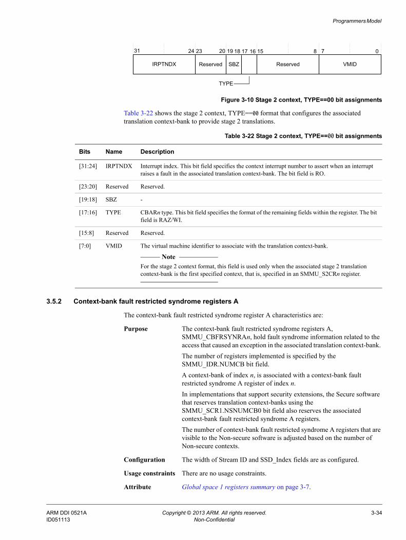
Programmers Model
Figure 3-10 Stage 2 context, TYPE==00 bit assignments
Table 3-22 shows the stage 2 context, TYPE==00 format that configures the associated translation context-bank to provide stage 2 translations.
3.5.2 Context-bank fault restricted syndrome registers A
The context-bank fault restricted syndrome register A characteristics are:
Purpose The context-bank fault restricted syndrome registers A, SMMU_CBFRSYNRAn, hold fault syndrome information related to the access that caused an exception in the associated translation context-bank. The number of registers implemented is specified by the SMMU_IDR.NUMCB bit field.A context-bank of index n, is associated with a context-bank fault restricted syndrome A register of index n.In implementations that support security extensions, the Secure software that reserves translation context-banks using the SMMU_SCR1.NSNUMCB0 bit field also reserves the associated context-bank fault restricted syndrome A registers.The number of context-bank fault restricted syndrome A registers that are visible to the Non-secure software is adjusted based on the number of Non-secure contexts.
Configuration The width of Stream ID and SSD_Index fields are as configured.
Usage constraints There are no usage constraints.
Attribute Global space 1 registers summary on page 3-7.
31 078
TYPE
24 23 20 19 18 17 16 15
IRPTNDX Reserved ReservedSBZ VMID
Table 3-22 Stage 2 context, TYPE==00 bit assignments
Bits Name Description
[31:24] IRPTNDX Interrupt index. This bit field specifies the context interrupt number to assert when an interrupt raises a fault in the associated translation context-bank. The bit field is RO.
[23:20] Reserved Reserved.
[19:18] SBZ -
[17:16] TYPE CBARn type. This bit field specifies the format of the remaining fields within the register. The bit field is RAZ/WI.
[15:8] Reserved Reserved.
[7:0] VMID The virtual machine identifier to associate with the translation context-bank.
Note For the stage 2 context format, this field is used only when the associated stage 2 translation context-bank is the first specified context, that is, specified in an SMMU_S2CRn register.
ARM DDI 0521A Copyright © 2013 ARM. All rights reserved. 3-34ID051113 Non-Confidential

Programmers Model
Figure 3-11 shows the bit assignments.
Figure 3-11 Context-bank restricted syndrome register bit assignments
Table 3-23 shows the bit assignments.
31 030 16 15 14
Reserved
SSD_Index Stream ID
Table 3-23 Context-bank restricted syndrome register bit assignments
Bits Name Description
[31] Reserved Reserved.
[30:16] SSD_Index SSD index of transaction that causes a fault.
Note This field is only accessible to Secure configuration accesses. Non-secure configuration accesses treat this field as RAZ/WI.
[15] Reserved Reserved.
[14:0] Stream ID The stream ID of the transaction that causes a fault.
ARM DDI 0521A Copyright © 2013 ARM. All rights reserved. 3-35ID051113 Non-Confidential
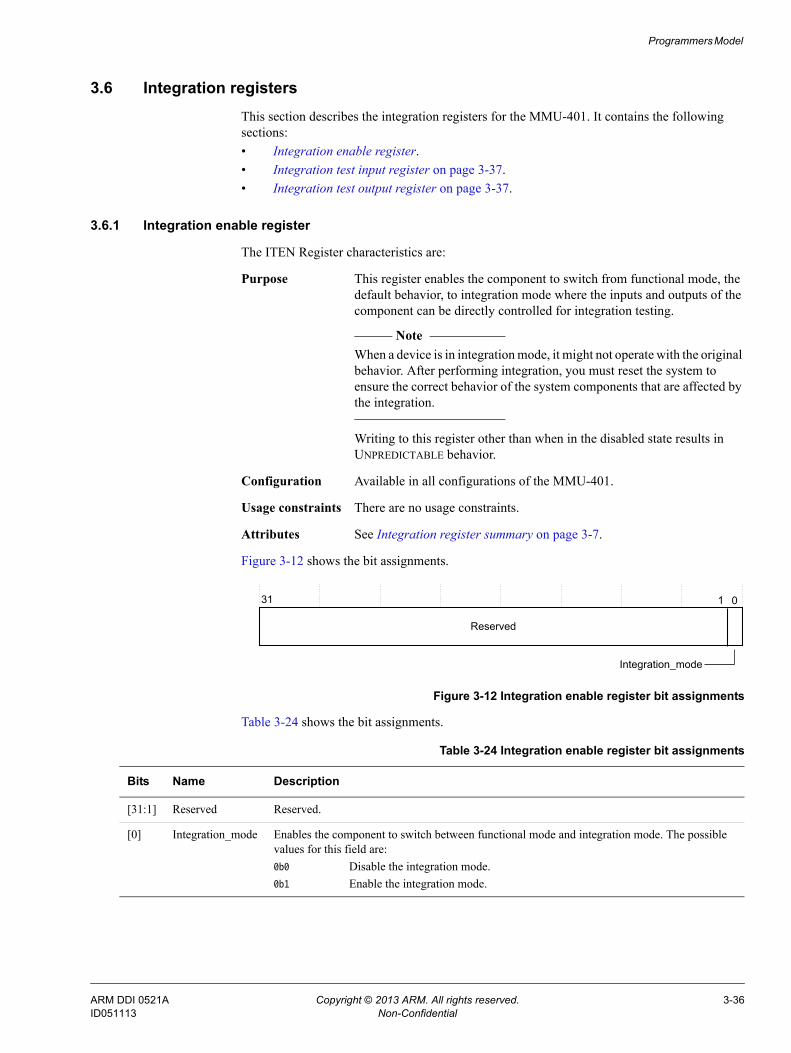
Programmers Model
3.6 Integration registersThis section describes the integration registers for the MMU-401. It contains the following sections: • Integration enable register.• Integration test input register on page 3-37.• Integration test output register on page 3-37.
3.6.1 Integration enable register
The ITEN Register characteristics are:
Purpose This register enables the component to switch from functional mode, the default behavior, to integration mode where the inputs and outputs of the component can be directly controlled for integration testing.
Note When a device is in integration mode, it might not operate with the original
behavior. After performing integration, you must reset the system to ensure the correct behavior of the system components that are affected by the integration.
Writing to this register other than when in the disabled state results in UNPREDICTABLE behavior.
Configuration Available in all configurations of the MMU-401.
Usage constraints There are no usage constraints.
Attributes See Integration register summary on page 3-7.
Figure 3-12 shows the bit assignments.
Figure 3-12 Integration enable register bit assignments
Table 3-24 shows the bit assignments.
31 01
Integration_mode
Reserved
Table 3-24 Integration enable register bit assignments
Bits Name Description
[31:1] Reserved Reserved.
[0] Integration_mode Enables the component to switch between functional mode and integration mode. The possible values for this field are:0b0 Disable the integration mode.0b1 Enable the integration mode.
ARM DDI 0521A Copyright © 2013 ARM. All rights reserved. 3-36ID051113 Non-Confidential
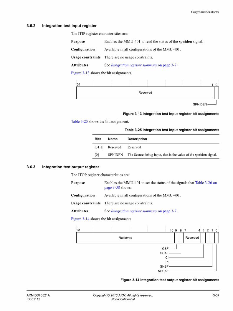
Programmers Model
3.6.2 Integration test input register
The ITIP register characteristics are:
Purpose Enables the MMU-401 to read the status of the spniden signal.
Configuration Available in all configurations of the MMU-401.
Usage constraints There are no usage constraints.
Attributes See Integration register summary on page 3-7.
Figure 3-13 shows the bit assignments.
Figure 3-13 Integration test input register bit assignments
Table 3-25 shows the bit assignment.
3.6.3 Integration test output register
The ITOP register characteristics are:
Purpose Enables the MMU-401 to set the status of the signals that Table 3-26 on page 3-38 shows.
Configuration Available in all configurations of the MMU-401.
Usage constraints There are no usage constraints.
Attributes See Integration register summary on page 3-7.
Figure 3-14 shows the bit assignments.
Figure 3-14 Integration test output register bit assignments
31 01
SPNIDEN
Reserved
Table 3-25 Integration test input register bit assignments
Bits Name Description
[31:1] Reserved Reserved.
[0] SPNIDEN The Secure debug input, that is the value of the spniden signal.
31 07810 9
GSFSCAF
3 2 14
CIPI
GNSFNSCAF
Reserved Reserved
ARM DDI 0521A Copyright © 2013 ARM. All rights reserved. 3-37ID051113 Non-Confidential

Programmers Model
Table 3-26 shows the bit assignments
Table 3-26 Integration test output register bit assignments
Bits Name Description
[31:10] - Reserved.
[9] GSF Global Secure fault. The value of this bit is equal to the value of the glbl_flt_irpt_s signal.
[8] SCAF Secure configuration access fault. The value of this bit is equal to the value of the cfg_flt_irpt_s signal.
[7:4] - Reserved.
[3] CI Context interrupt. The value of this bit is equal to the value of the cxt_irpt_ns signal.
[2] PI Performance interrupt. The value of this bit is equal to the value of the prf_irpt signal.
[1] GNSF Global Non-secure fault. The value of this bit is equal to the value of the glbl_flt_irpt_ns signal.
[0] NSCAF Non-secure configuration access fault. The value of this bit is equal to the value of the cfg_flt_irpt_ns signal.
ARM DDI 0521A Copyright © 2013 ARM. All rights reserved. 3-38ID051113 Non-Confidential

Programmers Model
3.7 Performance monitoring registersThis section describes the performance monitoring registers of the MMU-401, described in the following sections:• Performance monitor counter group configuration registers.• Performance monitor counter group stream match registers on page 3-40.• Performance monitor configuration register on page 3-41.• Performance monitor control register on page 3-42.• Performance monitor authentication status register on page 3-43.• Performance monitor device type register on page 3-45.
3.7.1 Performance monitor counter group configuration registers
The performance monitor counter group configuration registers characteristics are:
Purpose The performance monitor counter group configuration registers, PMCGCRn, control the behavior of a counter group.
Configuration Available in all configurations of the MMU-401.
Usage constraints There are no usage constraints.
Attributes Performance monitoring registers summary on page 3-8.
Figure 3-15 shows the bit assignments.
Figure 3-15 Performance monitor counter group configuration registers bit assignments
Table 3-27 shows the bit assignments.
31 07828 27 24 23 22 16 15 12 11 10 9
ReservedCEN
CBAENTCEFCFG
CGNC SIDG NDXReserved Reserved
Table 3-27 Performance monitor counter group configuration register bit assignments
Bits Name Description
[31:28] - Reserved.
[27:24] CGNC Counter group number of counters. This bit field indicates the number of counters in the counter group. This bit field is RO/WI. For the MMU-401, the value of this bit field is fixed at 3.
[23] - Reserved.
[22:16] SIDG Stream ID group. This bit field indicates the stream ID group to which the counter group is associated. This field is RO/WI. For the MMU-401, the value of this bit field is set to 0 to indicate that only one group is present
[15:12] - Reserved.
[11] CEN Count enable. This bit indicates the performance monitor count enable value for the counter group.
ARM DDI 0521A Copyright © 2013 ARM. All rights reserved. 3-39ID051113 Non-Confidential

Programmers Model
3.7.2 Performance monitor counter group stream match registers
The performance monitor counter group stream match registers characteristics are:
Purpose The performance monitor counter group stream match registers, PMCGSMRn, specify the stream ID-based filtering of events that are counted in a counter group.The number of ID and MASK bits is configured for Stream_ID_Width as the CoreLink MMU-401 System Memory Management Unit AMBA Designer (ADR-400) User Guide Supplement describes. The unimplemented bits are RAZ/WI. An implementation provides the same number of ID and MASK bits for every implemented PMCGSMRn register.You can enable the stream ID event filtering using the corresponding PMCGCRn.TCEFCFG field.
Configuration The width of the ID and MASK fields is equal to the configured STREAM_ID_WIDTH.
Usage constraints There are no usage constraints.
Attributes Performance monitoring registers summary on page 3-8.
Figure 3-16 shows the bit assignments.
Figure 3-16 Performance monitor counter group stream match registers bit assignments
[10] CBAEN Context-bank assignment enable. The possible values of this bit are:0b0 Do not reveal the counter group n in translation context-bank specified by the
PMCGCRn.NDX bit.0b1 Reveal the counter group n in the translation context-bank specified by the
PMCGCRn.NDX bit.If PMCGCRn.CBAEN==0b1 and PMCGCRn.TCEFCFG!=0b10 or 0b01, then the value of this bit is UNPREDICTABLE.
[9:8] TCEFCFG Translation context event filtering configuration. The possible values of this bit field are:0b00 Count events on a global basis.0b01 Count events restricted to a match in the corresponding PMCGSMRn register.0b10 Count Events restricted to a translation context-bank indicated by the
PMCGCRn.NDX bit.0b11 Reserved.
[7:0] NDX Index. This bit is interpreted based on the value of the PMCGCRn.TCEFCFG bit, and is only valid if PMCGCRn.TCEFCFG==0b10 else it is Reserved.
Table 3-27 Performance monitor counter group configuration register bit assignments (continued)
Bits Name Description
31 016 15 STREAM_ID_WIDTH-1
Reserved
15+STREAM_ID_WIDTH
MASK ID
ARM DDI 0521A Copyright © 2013 ARM. All rights reserved. 3-40ID051113 Non-Confidential

Programmers Model
Table 3-28 shows the performance monitor counter group stream match registers bit assignments.
3.7.3 Performance monitor configuration register
The performance monitor configuration register characteristics are:
Purpose The performance monitor configuration register, PMCFG, contains Performance Monitoring Unit (PMU)-specific configuration data.
Configuration Available in all configurations of the MMU-401.
Usage constraints There are no usage constraints.
Attributes Performance monitoring registers summary on page 3-8
Figure 3-17 shows the bit assignments.
Figure 3-17 Performance Monitor Configuration Register bit assignments
Table 3-29 shows the bit assignments.
Table 3-28 Performance monitor counter group stream match registers bit assignments
Bits Name Description
[31] - Reserved.
[15+STREAM_ID_WIDTH:16] MASK Mask. This bit field identifies whether the stream ID is ignored:MASK[i]==0b1 ID[i] is ignored.MASK[i]==0b0 ID[i] is relevant to the matched value.
[15:STREAM_ID_WIDTH] - Reserved.
[STREAM_ID_WIDTH-1:0] ID Stream ID to match.
31 07824 23 20 19 18 17 16 15 14 13 12 11 10
CCCCD
EXNAWT
UEN
Reserved
NCG Reserved NSIZE
Table 3-29 Performance Monitor Configuration Register bit assignments
Bits Name Reset value Description
[31:24] NCG 0b0 Number of counter groups. The number of counter groups is NCG+1.
[23:20] Reserved 0b0 Reserved.
[19] UEN 0b0 User enable. Read as 0b0, indicating that the user enable is not supported.
[18] Reserved 0b0 Reserved.
[17] Reserved 0b0 Reserved.
ARM DDI 0521A Copyright © 2013 ARM. All rights reserved. 3-41ID051113 Non-Confidential

Programmers Model
3.7.4 Performance monitor control register
The performance monitor control register characteristics are:
Purpose The performance monitor control register, PMCR, provides information about the performance monitor implementation, including the number of counters implemented, and configures and controls the counters.
Configuration Available in all configurations of the MMU-401.
Usage constraints There are no usage constraints.
Attributes Performance monitoring registers summary on page 3-8.
Figure 3-18 shows the bit assignments.
Figure 3-18 Performance monitor control register bit assignments
[16] EX 0b1 Event export. Reads as 0b1, indicating that the event export is supported. This bit is writable.
[15] CCD 0b0 Cycle counter prescale. Reads as 0b0, indicating that the prescale cycle counter is not implemented.
[14] CC 0b0 Cycle Counter. Reads as 0b0, indicating that the cycle counter is not implemented.
[13] Reserved 0b0 Reads as 0b0.
[12:11] SIZE 0b11 Counter size. Reads as 0b11 indicating 32-bit event counters.
[10:8] Reserved 0b111 Reads as 0b111.
[7:0] N 0b10 Indicates the number of implemented event counters. The number of implemented event counters is N+1.
Table 3-29 Performance Monitor Configuration Register bit assignments (continued)
Bits Name Reset value Description
31 0345 2
Reserved, UNK/SBZ
1
X P EReserved, UNK/SBZP
ARM DDI 0521A Copyright © 2013 ARM. All rights reserved. 3-42ID051113 Non-Confidential

Programmers Model
Table 3-30 shows the bit assignments.
Table 3-31 shows the action on writes to the count enable bit.
3.7.5 Performance monitor authentication status register
The performance monitor authentication status register characteristics are:
Purpose The performance monitor authentication status register, SMMU_CBn_AUTHSTATUS, indicates the implemented debug features and provides the current values of the configuration inputs that determine the debug permission. The returned value depends on whether the performance monitor implements the ARM security extension authentication model.
Table 3-30 Performance monitor control register bit assignments
Bits Name Reset value Description
[31:5] Reserved, UNK/SBZP - Reserved.
[4] X 0b0 Export enable. This bit is used to permit events to export to another debug device, such as Embedded Trace Macrocells (ETM™), over an event bus. If the implementation does not include the required event bus, this bit reads as 0b0 and ignores writes. This bit does not affect the generation of performance monitor interrupts that can be implemented as a signal exported from the core to an interrupt controller. The possible values of this bit are:0b0 Export of events is disabled.0b1 Export of events is enabled.
[3:2] Reserved, UNK/SBZP - Reserved.
[1] P 0b0 Event counter reset. This is a WO bit. The effects of writing to this bit are:0b0 No action.0b1 Reset all event counters to 0. If the cycle counter is implemented,
the cycle counter is not reset.
Note Resetting the event counter does not clear any overflow flags to 0.
This bit always reads as 0b0.
[0] E 0b0 Enable. The possible values of this bit are:0b0 All counters, including PMCCNTR, are disabled.0b1 All counters are enabled.Overflow interrupts are enabled only if the event counters are enabled. Writes to the bit request a stage change. See Table 3-31.
Table 3-31 Action on writes to the count enable bit
Old value New value Action on write
0b0 0b0 No action.
0b0 0b1 Start event.
0b1 0b0 End event.
0b1 0b1 No action.
ARM DDI 0521A Copyright © 2013 ARM. All rights reserved. 3-43ID051113 Non-Confidential
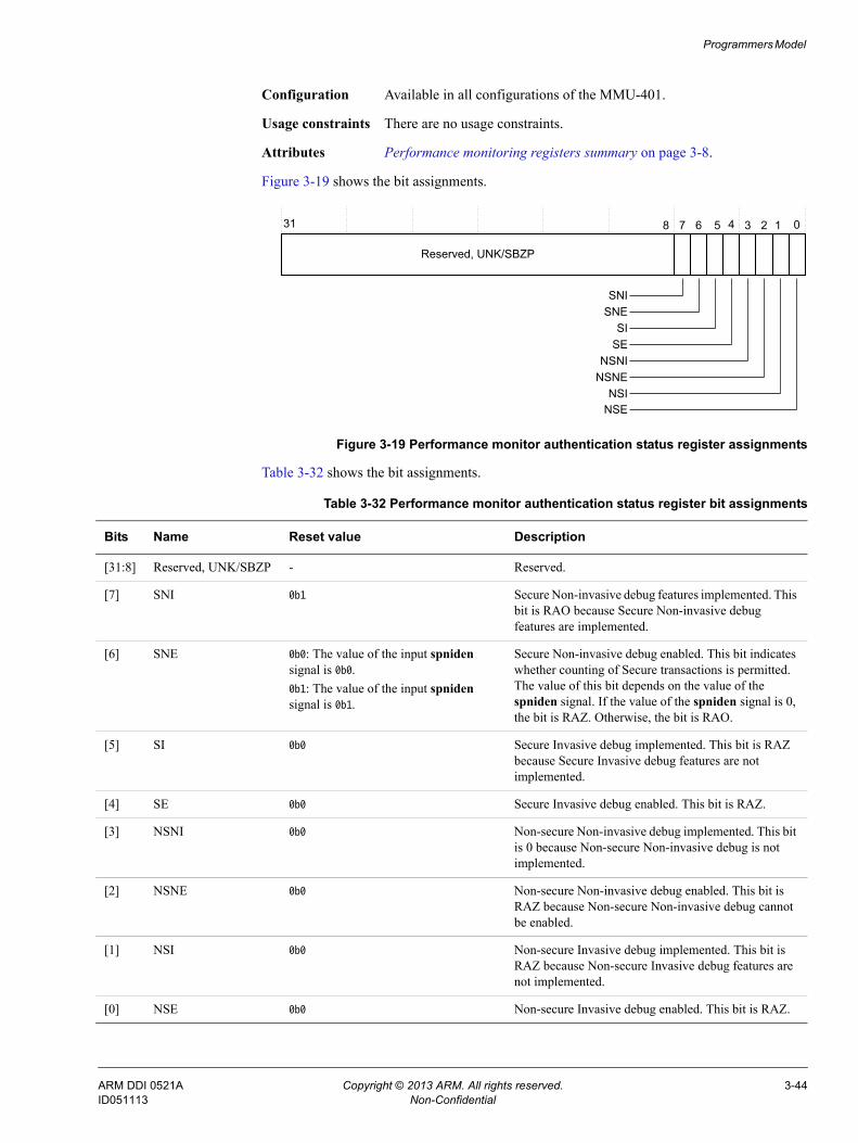
Programmers Model
Configuration Available in all configurations of the MMU-401.
Usage constraints There are no usage constraints.
Attributes Performance monitoring registers summary on page 3-8.
Figure 3-19 shows the bit assignments.
Figure 3-19 Performance monitor authentication status register assignments
Table 3-32 shows the bit assignments.
31 0345
SNI
2
SNE
1
SENSNI
7 68
NSNENSI
NSE
SI
Reserved, UNK/SBZP
Table 3-32 Performance monitor authentication status register bit assignments
Bits Name Reset value Description
[31:8] Reserved, UNK/SBZP - Reserved.
[7] SNI 0b1 Secure Non-invasive debug features implemented. This bit is RAO because Secure Non-invasive debug features are implemented.
[6] SNE 0b0: The value of the input spniden signal is 0b0.0b1: The value of the input spniden signal is 0b1.
Secure Non-invasive debug enabled. This bit indicates whether counting of Secure transactions is permitted. The value of this bit depends on the value of the spniden signal. If the value of the spniden signal is 0, the bit is RAZ. Otherwise, the bit is RAO.
[5] SI 0b0 Secure Invasive debug implemented. This bit is RAZ because Secure Invasive debug features are not implemented.
[4] SE 0b0 Secure Invasive debug enabled. This bit is RAZ.
[3] NSNI 0b0 Non-secure Non-invasive debug implemented. This bit is 0 because Non-secure Non-invasive debug is not implemented.
[2] NSNE 0b0 Non-secure Non-invasive debug enabled. This bit is RAZ because Non-secure Non-invasive debug cannot be enabled.
[1] NSI 0b0 Non-secure Invasive debug implemented. This bit is RAZ because Non-secure Invasive debug features are not implemented.
[0] NSE 0b0 Non-secure Invasive debug enabled. This bit is RAZ.
ARM DDI 0521A Copyright © 2013 ARM. All rights reserved. 3-44ID051113 Non-Confidential
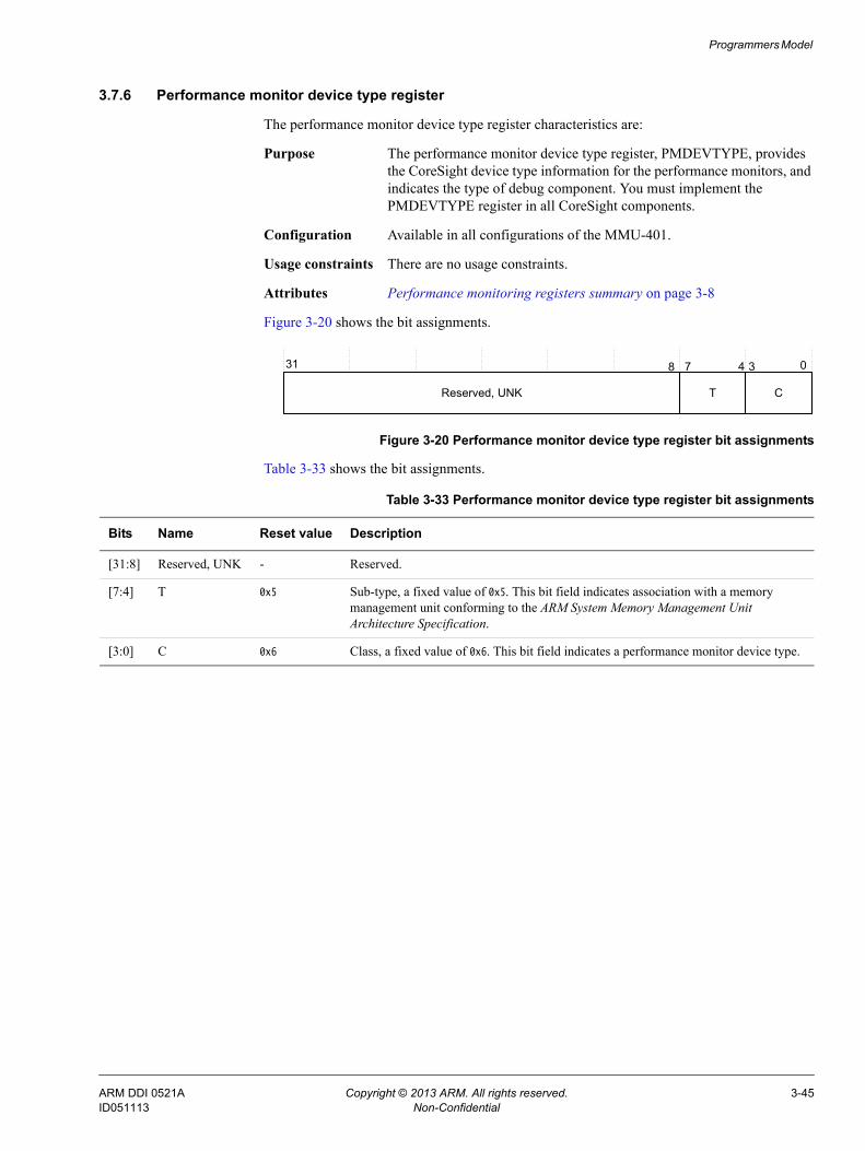
Programmers Model
3.7.6 Performance monitor device type register
The performance monitor device type register characteristics are:
Purpose The performance monitor device type register, PMDEVTYPE, provides the CoreSight device type information for the performance monitors, and indicates the type of debug component. You must implement the PMDEVTYPE register in all CoreSight components.
Configuration Available in all configurations of the MMU-401.
Usage constraints There are no usage constraints.
Attributes Performance monitoring registers summary on page 3-8
Figure 3-20 shows the bit assignments.
Figure 3-20 Performance monitor device type register bit assignments
Table 3-33 shows the bit assignments.
31 078 4 3
Reserved, UNK T C
Table 3-33 Performance monitor device type register bit assignments
Bits Name Reset value Description
[31:8] Reserved, UNK - Reserved.
[7:4] T 0x5 Sub-type, a fixed value of 0x5. This bit field indicates association with a memory management unit conforming to the ARM System Memory Management Unit Architecture Specification.
[3:0] C 0x6 Class, a fixed value of 0x6. This bit field indicates a performance monitor device type.
ARM DDI 0521A Copyright © 2013 ARM. All rights reserved. 3-45ID051113 Non-Confidential

Programmers Model
3.8 Security state determination address spaceThe MMU-401 security state determination address space characteristics are:
Purpose The MMU-401 security state determination address space, SMMU_SSDR, is part of the translation process.The security state determination address space provides an indication of whether each SSD index is enabled for the Secure or Non-secure domain. The address space is only accessible to Secure memory transactions.One bit is provided for each SSD index value. The MMU-401 supports an SSD index of up to 15 bits in size, corresponding to a total possible indication state of 4KB.The address space might not be fully populated, depending on the implemented page size and the SSD index width. The SSD index width can be read from the SMMU_IDR1.NUMSSDNDXB bit field. Unimplemented SSD index bits are read as zero. The security state determination register bits corresponding to values above the implemented SSD index size are read as UNK/SBOP.The security state determination bits can have fixed values that correspond to SSD index values that have a fixed Secure or Non-secure ownership. Software can detect programmable bits by using a read-modify-write sequence.The security state determination registers are implemented as shown in Implementation options for synthesis on page 1-5. The MMU-401 implementation and the system it is integrated in can use alternative means to resolve the security status of transactions. The SMMU_IDR1.SSDTP bit field indicates the presence of the security state determination table. In implementations where the registers are not present, this address space is UNK/SBOP.
Configuration Available in all configurations of the MMU-401.
Usage constraints There are no usage constraints.
Attributes Security state determination address space summary on page 3-8.
Table 3-34 shows the security state determination address space layout in terms of offsets from SMMU_GSSD_BASE.
If the security state determination register space is implemented, the behavior of each SMMU_SSDRn bit is:
// SMMU_SSDRn selected using SSD_Index<width>if (SMMU_SSDRn[SSD_Index<width>] == 1) {
// Transaction is Non-secure} else {
Table 3-34 Security state determination address space
Offset Name Description
0x000 SMMU_SSDR0 Corresponds to SSD index values in the range 0-31.
0x004 SMMU_SSDR1 Corresponds to SSD index values in the range 32-63.
0x008 - 0xFFC SMMU_SSDR1023 - SMMU_SSDR2 Corresponds to SSD index values in the range 64-32767.
0x01000 - (PAGESIZE-0x4) Reserved Reserved.
ARM DDI 0521A Copyright © 2013 ARM. All rights reserved. 3-46ID051113 Non-Confidential
Programmers Model
// Transaction is Secure }
In this example, the bits of the SMMU_SSDRn register are used to determine whether a master that performs the transactions is Secure or Non-secure. The example uses an SSD sideband signal, the width of which can be in the range 0-15. If the bit of the SMMU_SSDRn register is set to 0b1, the master is Non-secure, otherwise it is Secure.
ARM DDI 0521A Copyright © 2013 ARM. All rights reserved. 3-47ID051113 Non-Confidential
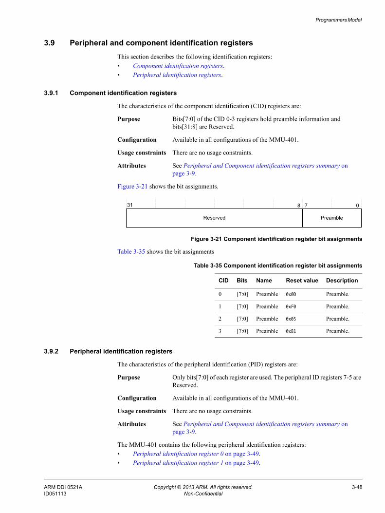
Programmers Model
3.9 Peripheral and component identification registersThis section describes the following identification registers: • Component identification registers.• Peripheral identification registers.
3.9.1 Component identification registers
The characteristics of the component identification (CID) registers are:
Purpose Bits[7:0] of the CID 0-3 registers hold preamble information and bits[31:8] are Reserved.
Configuration Available in all configurations of the MMU-401.
Usage constraints There are no usage constraints.
Attributes See Peripheral and Component identification registers summary on page 3-9.
Figure 3-21 shows the bit assignments.
Figure 3-21 Component identification register bit assignments
Table 3-35 shows the bit assignments
3.9.2 Peripheral identification registers
The characteristics of the peripheral identification (PID) registers are:
Purpose Only bits[7:0] of each register are used. The peripheral ID registers 7-5 are Reserved.
Configuration Available in all configurations of the MMU-401.
Usage constraints There are no usage constraints.
Attributes See Peripheral and Component identification registers summary on page 3-9.
The MMU-401 contains the following peripheral identification registers:• Peripheral identification register 0 on page 3-49.• Peripheral identification register 1 on page 3-49.
31 078
Reserved Preamble
Table 3-35 Component identification register bit assignments
CID Bits Name Reset value Description
0 [7:0] Preamble 0x0D Preamble.
1 [7:0] Preamble 0xF0 Preamble.
2 [7:0] Preamble 0x05 Preamble.
3 [7:0] Preamble 0xB1 Preamble.
ARM DDI 0521A Copyright © 2013 ARM. All rights reserved. 3-48ID051113 Non-Confidential
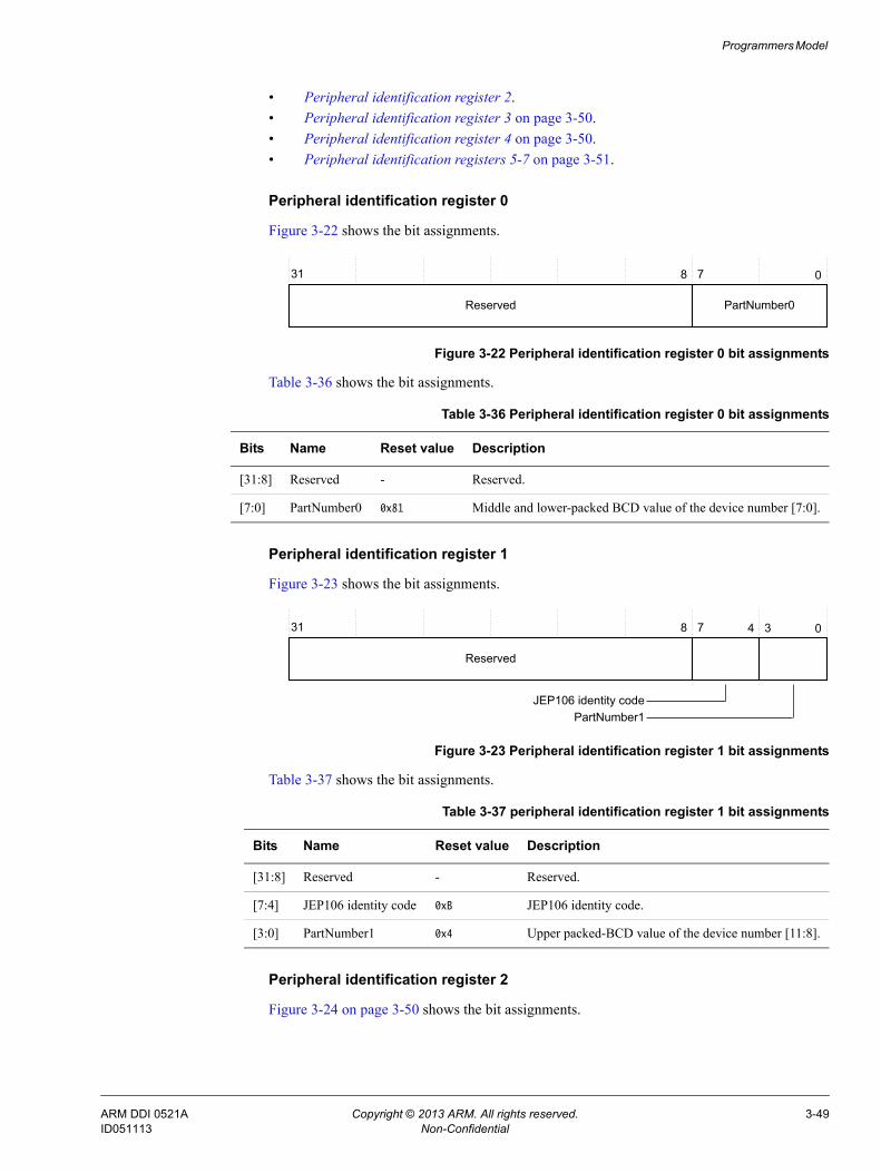
Programmers Model
• Peripheral identification register 2.• Peripheral identification register 3 on page 3-50.• Peripheral identification register 4 on page 3-50.• Peripheral identification registers 5-7 on page 3-51.
Peripheral identification register 0
Figure 3-22 shows the bit assignments.
Figure 3-22 Peripheral identification register 0 bit assignments
Table 3-36 shows the bit assignments.
Peripheral identification register 1
Figure 3-23 shows the bit assignments.
Figure 3-23 Peripheral identification register 1 bit assignments
Table 3-37 shows the bit assignments.
Peripheral identification register 2
Figure 3-24 on page 3-50 shows the bit assignments.
31 078
Reserved PartNumber0
Table 3-36 Peripheral identification register 0 bit assignments
Bits Name Reset value Description
[31:8] Reserved - Reserved.
[7:0] PartNumber0 0x81 Middle and lower-packed BCD value of the device number [7:0].
31 03478
PartNumber1JEP106 identity code
Reserved
Table 3-37 peripheral identification register 1 bit assignments
Bits Name Reset value Description
[31:8] Reserved - Reserved.
[7:4] JEP106 identity code 0xB JEP106 identity code.
[3:0] PartNumber1 0x4 Upper packed-BCD value of the device number [11:8].
ARM DDI 0521A Copyright © 2013 ARM. All rights reserved. 3-49ID051113 Non-Confidential
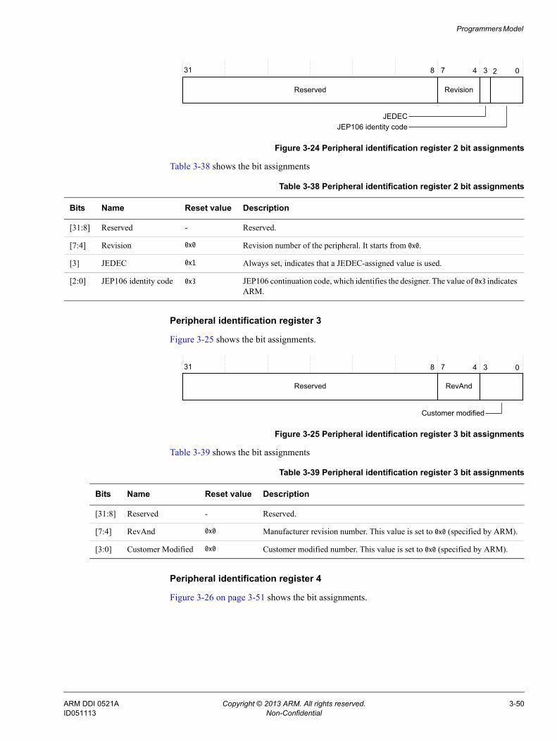
Programmers Model
Figure 3-24 Peripheral identification register 2 bit assignments
Table 3-38 shows the bit assignments
Peripheral identification register 3
Figure 3-25 shows the bit assignments.
Figure 3-25 Peripheral identification register 3 bit assignments
Table 3-39 shows the bit assignments
Peripheral identification register 4
Figure 3-26 on page 3-51 shows the bit assignments.
31 03478
JEP106 identity code
2
JEDEC
Reserved Revision
Table 3-38 Peripheral identification register 2 bit assignments
Bits Name Reset value Description
[31:8] Reserved - Reserved.
[7:4] Revision 0x0 Revision number of the peripheral. It starts from 0x0.
[3] JEDEC 0x1 Always set, indicates that a JEDEC-assigned value is used.
[2:0] JEP106 identity code 0x3 JEP106 continuation code, which identifies the designer. The value of 0x3 indicates ARM.
31 03478
Customer modified
Reserved RevAnd
Table 3-39 Peripheral identification register 3 bit assignments
Bits Name Reset value Description
[31:8] Reserved - Reserved.
[7:4] RevAnd 0x0 Manufacturer revision number. This value is set to 0x0 (specified by ARM).
[3:0] Customer Modified 0x0 Customer modified number. This value is set to 0x0 (specified by ARM).
ARM DDI 0521A Copyright © 2013 ARM. All rights reserved. 3-50ID051113 Non-Confidential
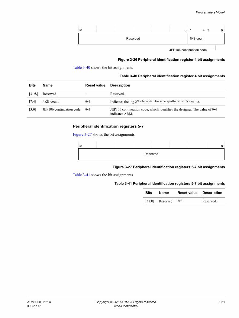
Programmers Model
Figure 3-26 Peripheral identification register 4 bit assignments
Table 3-40 shows the bit assignments
Peripheral identification registers 5-7
Figure 3-27 shows the bit assignments.
Figure 3-27 Peripheral identification registers 5-7 bit assignments
Table 3-41 shows the bit assignments.
31 03478
JEP106 continuation code
Reserved 4KB count
Table 3-40 Peripheral identification register 4 bit assignments
Bits Name Reset value Description
[31:8] Reserved - Reserved.
[7:4] 4KB count 0x4 Indicates the log 2Number of 4KB blocks occupied by the interface value.
[3:0] JEP106 continuation code 0x4 JEP106 continuation code, which identifies the designer. The value of 0x4 indicates ARM.
31 0
Reserved
Table 3-41 Peripheral identification registers 5-7 bit assignments
Bits Name Reset value Description
[31:0] Reserved 0x0 Reserved.
ARM DDI 0521A Copyright © 2013 ARM. All rights reserved. 3-51ID051113 Non-Confidential
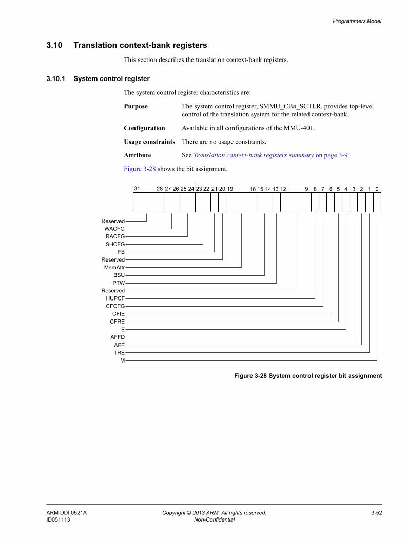
Programmers Model
3.10 Translation context-bank registersThis section describes the translation context-bank registers.
3.10.1 System control register
The system control register characteristics are:
Purpose The system control register, SMMU_CBn_SCTLR, provides top-level control of the translation system for the related context-bank.
Configuration Available in all configurations of the MMU-401.
Usage constraints There are no usage constraints.
Attribute See Translation context-bank registers summary on page 3-9.
Figure 3-28 shows the bit assignment.
Figure 3-28 System control register bit assignment
31 01234567828 27 26 25 24 23 22 21 20 19 16 15 14 13 12 9
TREAFE
AFFDE
CFRECFIE
CFCFGHUPCF
ReservedPTWBSU
MemAttrReserved
SHCFGRACFGWACFG
Reserved
M
FB
ARM DDI 0521A Copyright © 2013 ARM. All rights reserved. 3-52ID051113 Non-Confidential
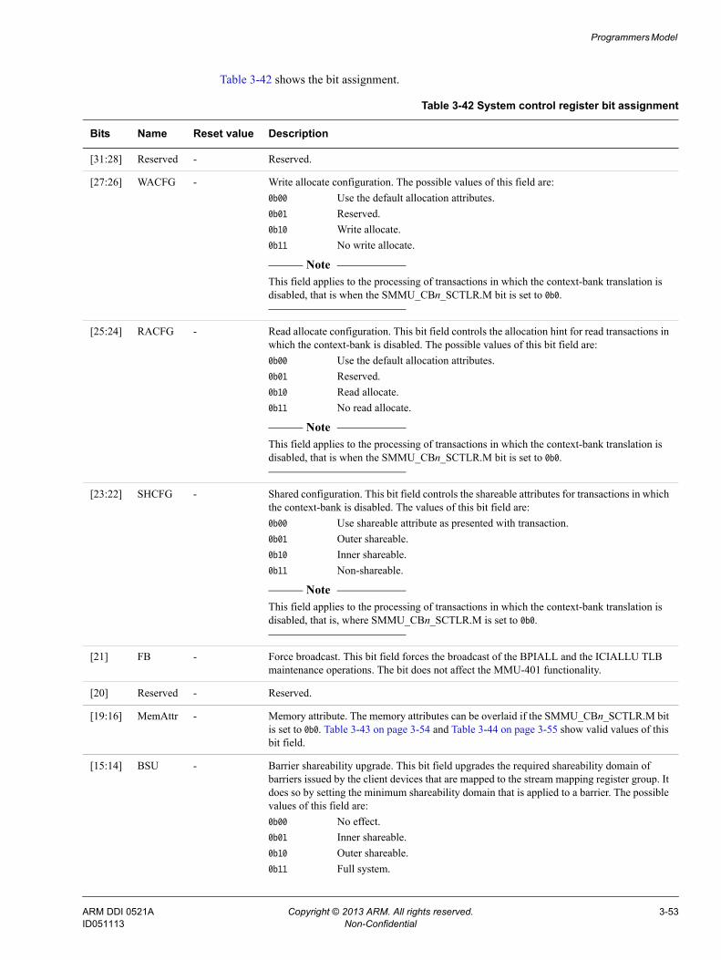
Programmers Model
Table 3-42 shows the bit assignment.
Table 3-42 System control register bit assignment
Bits Name Reset value Description
[31:28] Reserved - Reserved.
[27:26] WACFG - Write allocate configuration. The possible values of this field are:0b00 Use the default allocation attributes.0b01 Reserved.0b10 Write allocate.0b11 No write allocate.
Note This field applies to the processing of transactions in which the context-bank translation is disabled, that is when the SMMU_CBn_SCTLR.M bit is set to 0b0.
[25:24] RACFG - Read allocate configuration. This bit field controls the allocation hint for read transactions in which the context-bank is disabled. The possible values of this bit field are:0b00 Use the default allocation attributes.0b01 Reserved.0b10 Read allocate.0b11 No read allocate.
Note This field applies to the processing of transactions in which the context-bank translation is disabled, that is when the SMMU_CBn_SCTLR.M bit is set to 0b0.
[23:22] SHCFG - Shared configuration. This bit field controls the shareable attributes for transactions in which the context-bank is disabled. The values of this bit field are:0b00 Use shareable attribute as presented with transaction.0b01 Outer shareable.0b10 Inner shareable.0b11 Non-shareable.
Note This field applies to the processing of transactions in which the context-bank translation is disabled, that is, where SMMU_CBn_SCTLR.M is set to 0b0.
[21] FB - Force broadcast. This bit field forces the broadcast of the BPIALL and the ICIALLU TLB maintenance operations. The bit does not affect the MMU-401 functionality.
[20] Reserved - Reserved.
[19:16] MemAttr - Memory attribute. The memory attributes can be overlaid if the SMMU_CBn_SCTLR.M bit is set to 0b0. Table 3-43 on page 3-54 and Table 3-44 on page 3-55 show valid values of this bit field.
[15:14] BSU - Barrier shareability upgrade. This bit field upgrades the required shareability domain of barriers issued by the client devices that are mapped to the stream mapping register group. It does so by setting the minimum shareability domain that is applied to a barrier. The possible values of this field are:0b00 No effect.0b01 Inner shareable.0b10 Outer shareable.0b11 Full system.
ARM DDI 0521A Copyright © 2013 ARM. All rights reserved. 3-53ID051113 Non-Confidential

Programmers Model
Table 3-43 shows MemAttr bit values.
[13] Reserved - Reserved.
[12:9] Reserved - Reserved.
[8] HUPCF - Hit under previous context fault. The possible values of this bit are:0b0 Stall or terminate subsequent when a context fault occurs.0b1 Process subsequent transactions when a context fault occurs.
[7] CFCFG - Context fault configuration. The possible values of this bit are:0b0 Terminate.0b1 Stall.
[6] CFIE 0 Context fault interrupt enable. The possible values of this bit are:0b0 Do not raise an interrupt when a context fault occurs.0b1 Raise an interrupt when a context fault occurs.This field resets to 0b0.
[5] CFRE 0 Context fault report enable. The possible values of this bit are:0b0 Do not return an abort when a context fault occurs.0b1 Return an abort when a context fault occurs.
[4] E - Endianess. This field indicates the endianess format of translation table entries. The possible values of this bit are:0b0 Little endian format.0b1 Big endian format.
[3] AFFD - Access flag fault disable. This field determines whether access flag faults are reported if they are raised. The possible values of this bit are:0b0 Access flag faults are reported.0b1 Access flag faults are not reported.
[2] AFE 1 Access flag enable. This bit is UNK/SBOP.
[1] TRE 1 Type EXtension (TEX) remap enable. This bit is UNK/SBOP.
[0] M 0 The MMU-401 enable. This is a global enable bit for the translation context-bank. The possible values of this bit are:0b0 The MMU-401 behavior for the translation context-bank is disabled.0b1 The MMU-401 behavior for the translation context-bank is enabled.
Table 3-42 System control register bit assignment (continued)
Bits Name Reset value Description
Table 3-43 MemAttr bit values
Bits[3:2] Meaning
0b00 Strongly-ordered or the device memory.
0b01 Outer non-cacheable normal memory.
0b10 Outer write-through normal memory.
0b11 Outer write-back normal memory.
ARM DDI 0521A Copyright © 2013 ARM. All rights reserved. 3-54ID051113 Non-Confidential

Programmers Model
Table 3-44 shows secondary MemAttr bit values.
3.10.2 Translation table base control register
The translation table base control register characteristics are:
Purpose SMMU_CBn_TTBCR, the translation table base control register, provides additional configuration for the translation process.
Configuration Available in all configurations of the MMU-401.
Usage constraints Bit[31] is RAO/WI. PASize is always read as 2.
Attributes See Translation context-bank registers summary on page 3-9.
Figure 3-29 shows the bit assignments.
Figure 3-29 Translation table base control register bit assignments
Table 3-45 shows the bit assignments.
Table 3-44 Secondary MemAttr bit values
Bits[1:0] Meaning when bits[3:2] == 0b00 Meaning when bits[3:2]!= 0b00
0b00 Strongly-ordered Reserved.
0b01 Device Inner non-cacheable normal memory.
0b10 Device Inner write-through normal memory.
0b11 Device Inner write-back normal memory.
31 0567
PASize
30 1413 1211 10 89
IRGN0ORGN0
EAE
TG0Reserved
15161819
Reserved SH0 SL0 T0SZ
Table 3-45 Translation table base control register bit assignments
Bits Name Description
[31] EAE Extended address enable. This field always reads as 1. Writes are ignored.A value of 0b1 indicates that the translation system defined in the LPAE must be used. See the ARM Architecture Reference Manual ARMv7-A and ARMv7-R edition and the ARM Architecture Reference Manual, ARMv8, for ARMv8-A architecture profile for information on LPAE.
[30:19] Reserved Reserved.
[18:16] PASize The size of the PA. This field always reads as 0b10 and specifies support for 40-bit PA size.
[15] Reserved Reserved.
ARM DDI 0521A Copyright © 2013 ARM. All rights reserved. 3-55ID051113 Non-Confidential

Programmers Model
[14] TG0 The page granule size for the SMMU_CBn_TTBR0 register. The possible values of this field are:0b0 4KB pages.0b1 64KB pages.The reset value of this field is 0b0.Set TG0 and CBA2Rn.RW64 bits to 0b1 to enable 64KB granule sizes. See the ARM System Memory Management Unit Architecture Specification 64KB Translation Granule Supplement for information on the CBA2Rn register.
[13:12] SH0 Sharebility attributes for the memory associated with the translation page table walks using the SMMU_CBn_TTBR0 register.
[11:10] ORGN0 Outer cacheability attributes for the memory associated with the translation page table walks using the SMMU_CBn_TTBR0 register.
[9:8] IRGN0 Inner cacheability attributes for the memory associated with the translation page table walks using the SMMU_CBn_TTBR0 register.
[7:6] SL0 When the CBA2Rn.RW64 bit is set to 0, the SL0[1] bit is not considered. When bit [6] is set to 0b0, then the starting level for the SMMU_CBn_TTBR0 register addressed region is level 2.When bit [6] is set to 0b1, then the starting level for the SMMU_CBn_TTBR0 register addressed region is level 1.When the CBA2Rn.RW64 bit is set to 0b1 and the page size granule is 64KB, then the starting level for SMMU_CBn_TTBR0 is as follows:0b00 Level 3.0b01 Level 2.0b10 and 0b11 Return a transaction fault.When the CBA2Rn.RW64 bit is set to 0b1 and the page size granule is 4KB, then the starting level for SMMU_CBn_TTBR0 register is as follows:0b00 Level 2.0b01 Level 1.0b10 and 0b11 Return a transaction fault.
[5:0] T0SZ When the CBA2Rn.RW64 bit is set to 0b0, the addressed region is encoded as a 4-bit signed number that specifies the size of the region as 232-T0SZ.When the CBA2Rn.RW64 bit is 0b1, the addressed region is encoded as a 6-bit unsigned number that specifies the size of the region as 264-T0SZ.
Table 3-45 Translation table base control register bit assignments (continued)
Bits Name Description
ARM DDI 0521A Copyright © 2013 ARM. All rights reserved. 3-56ID051113 Non-Confidential

Appendix A Signal Descriptions
This appendix describes the MMU-401 signals, listed in the following sections:• Clock and resets on page A-2.• AXI3 signals on page A-3.• AXI4 signals on page A-8.• ACE-Lite signals on page A-12.• APB signals on page A-17.• LPI signals on page A-18.• Miscellaneous signals on page A-19.
ARM DDI 0521A Copyright © 2013 ARM. All rights reserved. A-1ID051113 Non-Confidential

Signal Descriptions
A.1 Clock and resetsThis section describes the clock and reset signals of the MMU-401.
Table A-1 shows the clock and reset signals of the PTW block.
Table A-2 shows the clock and reset signals of the TLB block.
Table A-1 PTW block clock and reset signals
Signal Width I/O Description
cclk 1 Input Clock for the PTW block.
cresetn 1 Input Reset for the PTW block.
Table A-2 TLB block clock and reset signals
Signal Width I/O Description
bclk 1 Input Clock for the TLB block.
bresetn 1 Input Reset for the TLB block.
ARM DDI 0521A Copyright © 2013 ARM. All rights reserved. A-2ID051113 Non-Confidential
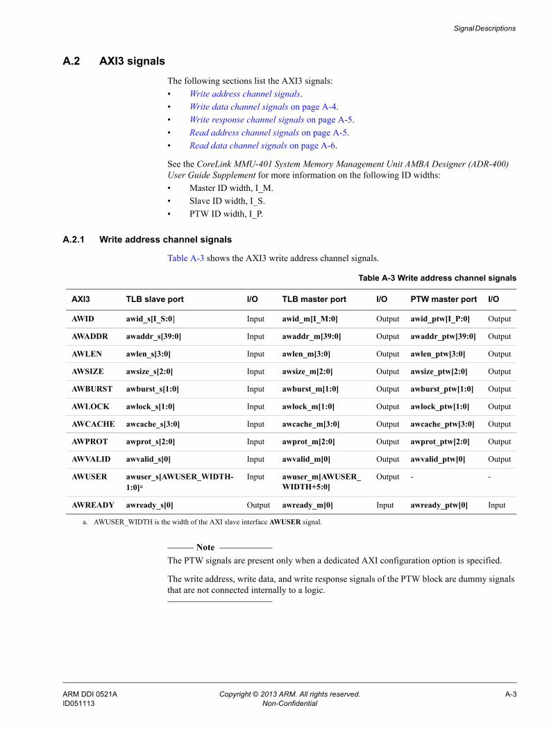
Signal Descriptions
A.2 AXI3 signalsThe following sections list the AXI3 signals:• Write address channel signals.• Write data channel signals on page A-4.• Write response channel signals on page A-5.• Read address channel signals on page A-5.• Read data channel signals on page A-6.
See the CoreLink MMU-401 System Memory Management Unit AMBA Designer (ADR-400) User Guide Supplement for more information on the following ID widths:• Master ID width, I_M.• Slave ID width, I_S.• PTW ID width, I_P.
A.2.1 Write address channel signals
Table A-3 shows the AXI3 write address channel signals.
Note The PTW signals are present only when a dedicated AXI configuration option is specified.
The write address, write data, and write response signals of the PTW block are dummy signals that are not connected internally to a logic.
Table A-3 Write address channel signals
AXI3 TLB slave port I/O TLB master port I/O PTW master port I/O
AWID awid_s[I_S:0] Input awid_m[I_M:0] Output awid_ptw[I_P:0] Output
AWADDR awaddr_s[39:0] Input awaddr_m[39:0] Output awaddr_ptw[39:0] Output
AWLEN awlen_s[3:0] Input awlen_m[3:0] Output awlen_ptw[3:0] Output
AWSIZE awsize_s[2:0] Input awsize_m[2:0] Output awsize_ptw[2:0] Output
AWBURST awburst_s[1:0] Input awburst_m[1:0] Output awburst_ptw[1:0] Output
AWLOCK awlock_s[1:0] Input awlock_m[1:0] Output awlock_ptw[1:0] Output
AWCACHE awcache_s[3:0] Input awcache_m[3:0] Output awcache_ptw[3:0] Output
AWPROT awprot_s[2:0] Input awprot_m[2:0] Output awprot_ptw[2:0] Output
AWVALID awvalid_s[0] Input awvalid_m[0] Output awvalid_ptw[0] Output
AWUSER awuser_s[AWUSER_WIDTH-1:0]a
Input awuser_m[AWUSER_WIDTH+5:0]
Output - -
AWREADY awready_s[0] Output awready_m[0] Input awready_ptw[0] Input
a. AWUSER_WIDTH is the width of the AXI slave interface AWUSER signal.
ARM DDI 0521A Copyright © 2013 ARM. All rights reserved. A-3ID051113 Non-Confidential

Signal Descriptions
A.2.2 Write data channel signals
Table A-4 shows the AXI3 write data channel signals for the slave port of the TLB block.
Table A-5 shows the AXI3 write data channel signals for the master port of the TLB block.
Table A-6 shows the AXI3 write data channel signals for the master port of the PTW block.
Table A-4 Write data channel signals for the slave port of the TLB block
AXI3 TLB slave port I/O
WID wid_s[I_S:0] Input
WDATA For 64-bit The data width is wdata_s[63:0].For 128-bit The data width is wdata_s[127:0].
Input
WSTRB For 64-bit The data width is wstrb_s[7:0].For 128-bit The data width is wstrb_s[15:0].
Input
WLAST wlast_s[0] Input
WVALID wvalid_s[0] Input
WUSER wuser_s[WUSER_WIDTH-1:0]a
a. WUSER_WIDTH is the width of the AXI slave interface WUSER signal.
Input
WREADY wready_s[0] Output
Table A-5 Write data channel signals for the master port of the TLB block
AXI3 TLB master port I/O
WID wid_m[I_M:0] Output
WDATA For 64-bit The data width is wdata_m[63:0].For 128-bit The data width is wdata_m[127:0].
Output
WSTRB For 64-bit The data width is wstrb_m[7:0].For 128-bit The data width is wstrb_m[15:0].
Output
WLAST wlast_m[0] Output
WVALID wvalid_m[0] Output
WUSER wuser_m[WUSER_WIDTH-1:0] Output
WREADY wready_m[0] Input
Table A-6 Write data channel signals for the master port of the PTW block
AXI3 PTW master port I/O
WID wid_ptw[I_P:0] Output
WDATA For 64-bit The data width is wdata_ptw[63:0].For 128-bit The data width is wdata_ptw[127:0].
Output
WSTRB For 64-bit The data width is wstrb_ptw[7:0].For 128-bit The data width is wstrb_ptw[15:0].
Output
WLAST wlast_ptw[0] Output
ARM DDI 0521A Copyright © 2013 ARM. All rights reserved. A-4ID051113 Non-Confidential

Signal Descriptions
A.2.3 Write response channel signals
Table A-7 shows the AXI3 write response channel signals.
A.2.4 Read address channel signals
Table A-8 shows the AXI3 read address channel signals.
WVALID wvalid_ptw[0] Output
WUSER - -
WREADY wready_ptw[0] Input
Table A-6 Write data channel signals for the master port of the PTW block (continued)
AXI3 PTW master port I/O
Table A-7 Write response channel signals
AXI3 TLB slave port I/O TLB master port I/O PTW master port I/O
BID bid_s[I_S:0] Output bid_m[I_M:0] Input bid_ptw[I_P:0] Input
BRESP bresp_s[1:0] Output bresp_m[1:0] Input bresp_ptw[1:0] Input
BVALID bvalid_s[0] Output bvalid_m[0] Input bvalid_ptw[0] Input
BUSER buser_s[BUSER_WIDTH-1:0]a
Output buser_m[BUSER_WIDTH-1:0] Input - -
BREADY bready_s[0] Input bready_m[0] Output bready_ptw[0] Output
a. BUSER_WIDTH is the width of the AXI slave interface BUSER signal.
Table A-8 Read address channel signals
AXI3 TLB slave port I/O TLB master port I/O PTW master port I/O
ARID arid_s[I_S:0] Input arid_m[I_M:0] Output arid_ptw[I_P:0] Output
ARADDR araddr_s[39:0] Input araddr_m[39:0] Output araddr_ptw[39:0] Output
ARLEN arlen_s[3:0] Input arlen_m[3:0] Output arlen_ptw[3:0] Output
ARSIZE arsize_s[2:0] Input arsize_m[2:0] Output arsize_ptw[2:0] Output
ARBURST arburst_s[1:0] Input arburst_m[1:0] Output arburst_ptw[1:0] Output
ARLOCK arlock_s[1:0] Input arlock_m[1:0] Output arlock_ptw[1:0] Output
ARCACHE arcache_s[3:0] Input arcache_m[3:0] Output arcache_ptw[3:0] Output
ARPROT arprot_s[2:0] Input arprot_m[2:0] Output arprot_ptw[2:0] Output
ARVALID arvalid_s[0] Input arvalid_m[0] Output arvalid_ptw[0] Output
ARUSER aruser_s[ARUSER_WIDTH-1:0]a
Input aruser_m[ARUSER_WIDTH+5:0] Output aruser_ptw[5:0] Output
ARREADY arready_s[0] Output arready_m[0] Input arready_ptw[0] Input
a. ARUSER_WIDTH is the width of the AXI slave interface ARUSER signal.
ARM DDI 0521A Copyright © 2013 ARM. All rights reserved. A-5ID051113 Non-Confidential

Signal Descriptions
A.2.5 Read data channel signals
Table A-9 shows the AXI3 read data channel signals for the slave port of the TLB block.
Table A-10 shows the AXI3 read data channel signals for the master port of the TLB block.
Table A-11 shows the AXI3 read data channel signals for the master port of the PTW block.
Table A-9 Read data channel signals for the slave port of the TLB block
AXI3 TLB slave port I/O
RID rid_s[I_S:0] Output
RDATA For 64-bit The data width is rdata_s[63:0].For 128-bit The data width is rdata_s[127:0].
Output
RRESP rresp_s[1:0] Output
RLAST rlast_s[0] Output
RVALID rvalid_s[0] Output
RUSER ruser_s[RUSER_WIDTH-1:0]a
a. RUSER_WIDTH is the width of the AXI slave interface RUSER signal.
Output
RREADY rready_s[0] Input
Table A-10 Read data channel signals for the master port of the TLB block
AXI3 TLB master port I/O
RID rid_m[I_M:0] Input
RDATA For 64-bit The data width is rdata_m[63:0].For 128-bit The data width is rdata_m[127:0].
Input
RRESP rresp_m[1:0] Input
RLAST rlast_m[0] Input
RVALID rvalid_m[0] Input
RUSER ruser_m[RUSER_WIDTH-1:0] Input
RREADY rready_m[0] Output
Table A-11 Read data channel signals for the master port of the PTW block
AXI3 PTW master port I/O
RID rid_ptw[I_P:0] Input
RDATA For 64-bit The data width is rdata_ptw[63:0].For 128-bit The data width is rdata_ptw[127:0].
Input
RRESP rresp_ptw[1:0] Input
RLAST rlast_ptw[0] Input
ARM DDI 0521A Copyright © 2013 ARM. All rights reserved. A-6ID051113 Non-Confidential
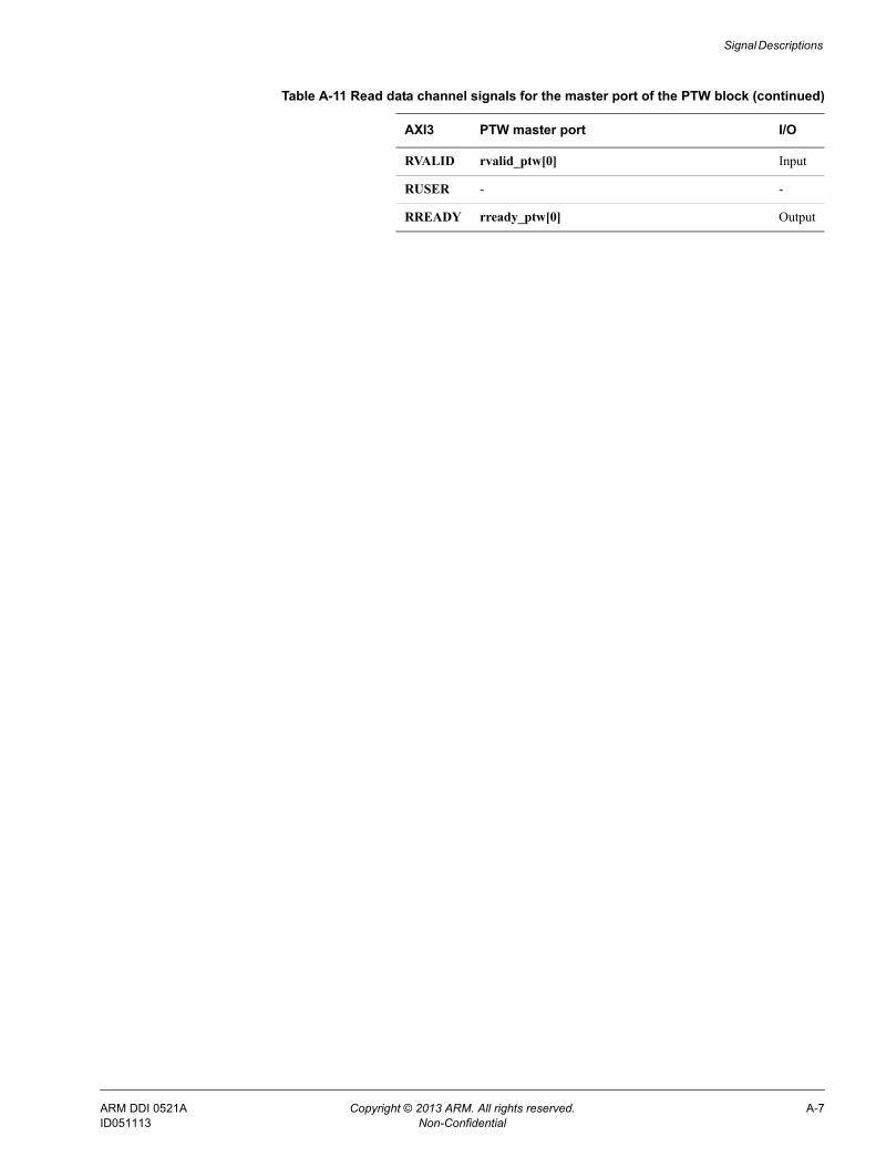
Signal Descriptions
RVALID rvalid_ptw[0] Input
RUSER - -
RREADY rready_ptw[0] Output
Table A-11 Read data channel signals for the master port of the PTW block (continued)
AXI3 PTW master port I/O
ARM DDI 0521A Copyright © 2013 ARM. All rights reserved. A-7ID051113 Non-Confidential

Signal Descriptions
A.3 AXI4 signalsThe following sections list the AXI4 signals:• Write address channel signals.• Write data channel signals on page A-9.• Write response channel signals on page A-10.• Read address channel signals on page A-10.• Read data channel signals on page A-11.
See the CoreLink MMU-401 System Memory Management Unit AMBA Designer (ADR-400) User Guide Supplement for more information on the following ID widths:• Master ID width, I_M.• Slave ID width, I_S.• PTW ID width, I_P.
A.3.1 Write address channel signals
Table A-12 shows the AXI4 write address channel signals.
Table A-12 Write address channel signals
AXI4 TLB slave port I/O TLB master port I/O PTW master port I/O
AWID awid_s[I_S:0] Input awid_m[I_M:0] Output awid_ptw[I_P:0] Output
AWADDR awaddr_s[39:0] Input awaddr_m[39:0] Output awaddr_ptw[39:0] Output
AWLEN awlen_s[7:0] Input awlen_m[7:0] Output awlen_ptw[7:0] Output
AWSIZE awsize_s[2:0] Input awsize_m[2:0] Output awsize_ptw[2:0] Output
AWBURST awburst_s[1:0] Input awburst_m[1:0] Output awburst_ptw[1:0] Output
AWLOCK awlock_s[0] Input awlock_m[0] Output awlock_ptw[0] Output
AWCACHE awcache_s[3:0] Input awcache_m[3:0] Output awcache_ptw[3:0] Output
AWPROT awprot_s[2:0] Input awprot_m[2:0] Output awprot_ptw[2:0] Output
AWVALID awvalid_s[0] Input awvalid_m[0] Output awvalid_ptw[0] Output
AWREGION awregion_s[3:0] Input awregion_m[3:0] Output awregion_ptw[3:0] Output
AWQOS awqos_s[3:0] Input awqos_m[3:0] Output awqos_ptw[3:0] Input
AWUSER awuser_s[AWUSER_WIDTH-1:0]
Input awuser_m[AWUSER_WIDTH+5:0]
Output - -
AWREADY awready_s[0] Output awready_m[0] Input awready_ptw[0] Output
ARM DDI 0521A Copyright © 2013 ARM. All rights reserved. A-8ID051113 Non-Confidential
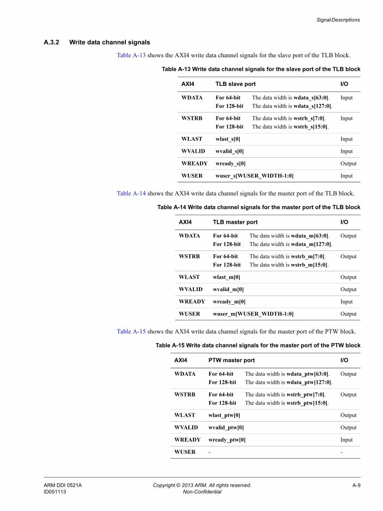
Signal Descriptions
A.3.2 Write data channel signals
Table A-13 shows the AXI4 write data channel signals for the slave port of the TLB block.
Table A-14 shows the AXI4 write data channel signals for the master port of the TLB block.
Table A-15 shows the AXI4 write data channel signals for the master port of the PTW block.
Table A-13 Write data channel signals for the slave port of the TLB block
AXI4 TLB slave port I/O
WDATA For 64-bit The data width is wdata_s[63:0].For 128-bit The data width is wdata_s[127:0].
Input
WSTRB For 64-bit The data width is wstrb_s[7:0].For 128-bit The data width is wstrb_s[15:0].
Input
WLAST wlast_s[0] Input
WVALID wvalid_s[0] Input
WREADY wready_s[0] Output
WUSER wuser_s[WUSER_WIDTH-1:0] Input
Table A-14 Write data channel signals for the master port of the TLB block
AXI4 TLB master port I/O
WDATA For 64-bit The data width is wdata_m[63:0].For 128-bit The data width is wdata_m[127:0].
Output
WSTRB For 64-bit The data width is wstrb_m[7:0].For 128-bit The data width is wstrb_m[15:0].
Output
WLAST wlast_m[0] Output
WVALID wvalid_m[0] Output
WREADY wready_m[0] Input
WUSER wuser_m[WUSER_WIDTH-1:0] Output
Table A-15 Write data channel signals for the master port of the PTW block
AXI4 PTW master port I/O
WDATA For 64-bit The data width is wdata_ptw[63:0].For 128-bit The data width is wdata_ptw[127:0].
Output
WSTRB For 64-bit The data width is wstrb_ptw[7:0].For 128-bit The data width is wstrb_ptw[15:0].
Output
WLAST wlast_ptw[0] Output
WVALID wvalid_ptw[0] Output
WREADY wready_ptw[0] Input
WUSER - -
ARM DDI 0521A Copyright © 2013 ARM. All rights reserved. A-9ID051113 Non-Confidential

Signal Descriptions
A.3.3 Write response channel signals
Table A-16 shows the AXI4 write response channel signals.
A.3.4 Read address channel signals
Table A-17 shows the AXI4 read address channel signals.
Table A-16 Write response channel signals
AXI4 TLB slave port I/O TLB master port I/O PTW master port I/O
BID bid_s[I_S:0] Output bid_m[I_M:0] Input bid_ptw[I_P:0] Input
BRESP bresp_s[1:0] Output bresp_m[1:0] Input bresp_ptw[1:0] Input
BVALID bvalid_s[0] Output bvalid_m[0] Input bvalid_ptw[0] Input
BUSER buser_s[BUSER_WIDTH-1:0]
Output buser_m[BUSER_WIDTH-1:0] Input - -
BREADY bready_s[0] Input bready_m[0] Output bready_ptw[0] Output
Table A-17 Read address channel signals
AXI4 TLB slave port I/O TLB master port I/O PTW master port I/O
ARID arid_s[I_S:0] Input arid_m[I_M:0] Output arid_ptw[I_P:0] Output
ARADDR araddr_s[39:0] Input araddr_m[39:0] Output araddr_ptw[39:0] Output
ARLEN arlen_s[7:0] Input arlen_m[7:0] Output arlen_ptw[7:0] Output
ARSIZE arsize_s[2:0] Input arsize_m[2:0] Output arsize_ptw[2:0] Output
ARBURST arburst_s[1:0] Input arburst_m[1:0] Output arburst_ptw[1:0] Output
ARLOCK arlock_s[0] Input arlock_m[0] Output arlock_ptw[0] Output
ARCACHE arcache_s[3:0] Input arcache_m[3:0] Output arcache_ptw[3:0] Output
ARPROT arprot_s[2:0] Input arprot_m[2:0] Output arprot_ptw[2:0] Output
ARVALID arvalid_s[0] Input arvalid_m[0] Output arvalid_ptw[0] Output
ARREGION arregion_s[3:0] Input arregion_m[3:0] Output arregion_ptw[3:0] Output
ARQOS arqos_s[3:0] Input arqos_m[3:0] Output arqos_ptw[3:0] Output
ARUSER aruser_s[ARUSER_WIDTH-1:0]
Input aruser_m[ARUSER_WIDTH+5:0] Output aruser_ptw[5:0] Output
ARREADY arready_s[0] Output arready_m[0] Input arready_ptw[0] Input
ARM DDI 0521A Copyright © 2013 ARM. All rights reserved. A-10ID051113 Non-Confidential

Signal Descriptions
A.3.5 Read data channel signals
Table A-18 shows the AXI4 read data channel signals for the slave port of the TLB block.
Table A-19 shows the AXI4 read data channel signals for the master port of the TLB block.
Table A-20 shows the AXI4 read data channel signals for the master port of the PTW block.
Table A-18 Read data channel signals for the slave port of the TLB block
AXI4 TLB slave port I/O
RID rid_s[I_S:0] Output
RDATA For 64-bit The data width is rdata_s[63:0].For 128-bit The data width is rdata_s[127:0].
Output
RRESP rresp_s[1:0] Output
RLAST rlast_s[0] Output
RVALID rvalid_s[0] Output
RUSER ruser_s[RUSER_WIDTH-1:0] Output
RREADY rready_s[0] Input
Table A-19 Read data channel signals for the master port of the TLB block
AXI4 TLB master port I/O
RID rid_m[I_M:0] Input
RDATA For 64-bit The data width is rdata_m[63:0].For 128-bit The data width is rdata_m[127:0].
Input
RRESP rresp_m[1:0] Input
RLAST rlast_m[0] Input
RVALID rvalid_m[0] Input
RUSER ruser_m[RUSER_WIDTH-1:0] Input
RREADY rready_m[0] Output
Table A-20 Read data channel signals for the master port of the PTW block
AXI4 PTW master port I/O
RID rid_ptw[I_P:0] Input
RDATA For 64-bit The data width is rdata_ptw[63:0].For 128-bit The data width is rdata_ptw[127:0].
Input
RRESP rresp_ptw[3:0] Input
RLAST rlast_ptw[0] Input
RVALID rvalid_ptw[0] Input
RUSER - Input
RREADY rready_ptw[0] Output
ARM DDI 0521A Copyright © 2013 ARM. All rights reserved. A-11ID051113 Non-Confidential

Signal Descriptions
A.4 ACE-Lite signalsThe following sections list the ACE-Lite signals:• Write address channel signals.• Write data channel signals on page A-13.• Write response channel signals on page A-14.• Read address channel signals on page A-14.• Read data channel signals on page A-15.• Snoop channel signals on page A-16.
See the CoreLink MMU-401 System Memory Management Unit AMBA Designer (ADR-400) User Guide Supplement for more information on the following ID widths:• Master ID width, I_M.• Slave ID width, I_S.• PTW ID width, I_P.
A.4.1 Write address channel signals
Table A-21 shows the ACE-Lite write address channel signals.
Table A-21 Write address channel signals
ACE-Lite TLB slave port I/O TLB master port I/O PTW master port I/O
AWID awid_s[I_S:0] Input awid_m[I_M:0] Output awid_ptw[I_P:0] Output
AWADDR awaddr_s[39:0] Input awaddr_m[39:0] Output awaddr_ptw[39:0] Output
AWLEN awlen_s[7:0] Input awlen_m[7:0] Output awlen_ptw[7:0] Output
AWSIZE awsize_s[2:0] Input awsize_m[2:0] Output awsize_ptw[2:0] Output
AWBURST awburst_s[1:0] Input awburst_m[1:0] Output awburst_ptw[1:0] Output
AWLOCK awlock_s[0] Input awlock_m[0] Output awlock_ptw[0] Output
AWCACHE awcache_s[3:0] Input awcache_m[3:0] Output awcache_ptw[3:0] Output
AWPROT awprot_s[2:0] Input awprot_m[2:0] Output awprot_ptw[2:0] Output
AWVALID awvalid_s[0] Input awvalid_m[0] Output awvalid_ptw[0] Output
AWREGION awregion_s[3:0] Input awregion_m[3:0] Output awregion_ptw[3:0] Output
AWQOS awqos_s[3:0] Input awqos_m[3:0] Output awqos_ptw[3:0] Output
AWSNOOP awsnoop_s[2:0] Input awsnoop_m[2:0] Output awsnoop_ptw[2:0] Output
AWBAR awbar_s[1:0] Input awbar_m[1:0] Output awbar_ptw[1:0] Output
AWDOMAIN awdomain_s[1:0] Input awdomain_m[1:0] Output awdomain_ptw[1:0] Output
AWUSER awuser_s[AWUSER_WIDTH+3:0]
Input awuser_m[AWUSER_WIDTH+3:0]
Output - -
AWREADY awready_s[0] Output awready_m[0] Input awready_ptw[0] Input
ARM DDI 0521A Copyright © 2013 ARM. All rights reserved. A-12ID051113 Non-Confidential

Signal Descriptions
A.4.2 Write data channel signals
Table A-22 shows the ACE-Lite write data channel signals for the slave port of the TLB block.
Table A-23 shows the ACE-Lite write data channel signals for the master port of the TLB block.
Table A-24 shows the ACE-Lite write data channel signals for the master port of the PTW block.
Table A-22 Write data channel signals for the slave port of the TLB block
ACE-Lite TLB slave port I/O
WDATA For 64-bit The data width is wdata_s[63:0].For 128-bit The data width is wdata_s[127:0].
Input
WSTRB For 64-bit The data width is wstrb_s[7:0].For 128-bit The data width is wstrb_s[15:0].
Input
WLAST wlast_s[0] Input
WVALID wvalid_s[0] Input
WUSER wuser_s[WUSER_WIDTH-1:0] Input
WREADY wready_s[0] Output
Table A-23 Write data channel signals for the master port of the TLB block
ACE-Lite TLB master port I/O
WDATA For 64-bit The data width is wdata_m[63:0].For 128-bit The data width is wdata_m[127:0].
Output
WSTRB For 64-bit The data width is wstrb_m[7:0].For 128-bit The data width is wstrb_m[15:0].
Output
WLAST wlast_m[0] Output
WVALID wvalid_m[0] Output
WUSER wuser_m[WUSER_WIDTH-1:0] Output
WREADY wready_m[0] Input
Table A-24 Write data channel signals for the master port of the PTW block
ACE-Lite PTW master port I/O
WDATA For 64-bit The data width is wdata_ptw[63:0].For 128-bit The data width is wdata_ptw[127:0].
Output
WSTRB For 64-bit The data width is wstrb_ptw[7:0].For 128-bit The data width is wstrb_ptw[15:0].
Output
WLAST wlast_ptw[0] Output
WVALID wvalid_ptw[0] Output
WUSER - -
WREADY wready_ptw[0] Input
ARM DDI 0521A Copyright © 2013 ARM. All rights reserved. A-13ID051113 Non-Confidential

Signal Descriptions
A.4.3 Write response channel signals
Table A-25 shows the ACE-Lite write response channel signals.
A.4.4 Read address channel signals
Table A-26 shows the ACE-Lite read address channel signals.
Table A-25 Write response channel signals
ACE-Lite TLB slave port I/O TLB master port I/O PTW master port I/O
BID bid_s[I_S:0] Input bid_m[I_M:0] Output bid_ptw[I_P:0] Output
BRESP bresp_s[1:0] Output bresp_m[1:0] Input bresp_ptw[1:0] Input
BVALID bvalid_s[0] Output bvalid_m[0] Input bvalid_ptw[0] Input
BUSER buser_s[BUSER_WIDTH-1:0]
Output buser_m[BUSER_WIDTH-1:0] Input - -
BREADY bready_s[0] Input bready_m[0] Output bready_ptw[0] Output
Table A-26 Read address channel signals
ACE-Lite TLB slave port I/O TLB master port I/O PTW master port I/O
ARID arid_s[I_S:0] Input arid_m[I_M:0] Output arid_ptw[I_P:0] Output
ARADDR araddr_s[39:0] Input araddr_m[39:0] Output araddr_ptw[39:0] Output
ARLEN arlen_s[7:0] Input arlen_m[7:0] Output arlen_ptw[7:0] Output
ARSIZE arsize_s[2:0] Input arsize_m[2:0] Output arsize_ptw[2:0] Output
ARBURST arburst_s[1:0] Input arburst_m[1:0] Output arburst_ptw[1:0] Output
ARLOCK arlock_s[0] Input arlock_m[0] Output arlock_ptw[0] Output
ARCACHE arcache_s[3:0] Input arcache_m[3:0] Output arcache_ptw[3:0] Output
ARPROT arprot_s[2:0] Input arprot_m[2:0] Output arprot_ptw[2:0] Output
ARVALID arvalid_s[0] Input arvalid_m[0] Output arvalid_ptw[0] Output
ARREGION arregion_s[3:0] Input arregion_m[3:0] Output arregion_ptw[3:0] Output
ARQOS arqos_s[3:0] Input arqos_m[3:0] Output arqos_ptw[3:0] Output
ARSNOOP arsnoop_s[3:0] Input arsnoop_m[3:0] Output arsnoop_ptw[3:0] Output
ARBAR arbar_s[1:0] Input arbar_m[1:0] Output arbar_ptw[1:0] Output
ARDOMAIN ardomain_s[1:0] Input ardomain_m[1:0] Output ardomain_ptw[1:0] Output
ARUSER aruser_s[ARUSER_WIDTH-1:0]
Input aruser_m[ARUSER_WIDTH+3:0]
Output aruser_ptw[3:0] Output
ARREADY arready_s[0] Output arready_m[0] Input arready_ptw[0] Input
ARM DDI 0521A Copyright © 2013 ARM. All rights reserved. A-14ID051113 Non-Confidential
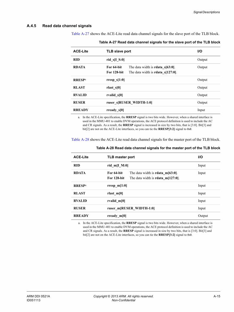
Signal Descriptions
A.4.5 Read data channel signals
Table A-27 shows the ACE-Lite read data channel signals for the slave port of the TLB block.
Table A-28 shows the ACE-Lite read data channel signals for the master port of the TLB block.
Table A-27 Read data channel signals for the slave port of the TLB block
ACE-Lite TLB slave port I/O
RID rid_s[I_S:0] Output
RDATA For 64-bit The data width is rdata_s[63:0].For 128-bit The data width is rdata_s[127:0].
Output
RRESPa
a. In the ACE-Lite specification, the RRESP signal is two bits wide. However, when a shared interface is used in the MMU-401 to enable DVM operations, the ACE protocol definition is used to include the AC and CR signals. As a result, the RRESP signal is increased in size by two bits, that is [3:0]. Bit[3] and bit[2] are not on the ACE-Lite interfaces, so you can tie the RRESP[3:2] signal to 0x0.
rresp_s[1:0] Output
RLAST rlast_s[0] Output
RVALID rvalid_s[0] Output
RUSER ruser_s[RUSER_WIDTH-1:0] Output
RREADY rready_s[0] Input
Table A-28 Read data channel signals for the master port of the TLB block
ACE-Lite TLB master port I/O
RID rid_m[I_M:0] Input
RDATA For 64-bit The data width is rdata_m[63:0].For 128-bit The data width is rdata_m[127:0].
Input
RRESPa
a. In the ACE-Lite specification, the RRESP signal is two bits wide. However, when a shared interface is used in the MMU-401 to enable DVM operations, the ACE protocol definition is used to include the AC and CR signals. As a result, the RRESP signal is increased in size by two bits, that is [3:0]. Bit[3] and bit[2] are not on the ACE-Lite interfaces, so you can tie the RRESP[3:2] signal to 0x0.
rresp_m[1:0] Input
RLAST rlast_m[0] Input
RVALID rvalid_m[0] Input
RUSER ruser_m[RUSER_WIDTH-1:0] Input
RREADY rready_m[0] Output
ARM DDI 0521A Copyright © 2013 ARM. All rights reserved. A-15ID051113 Non-Confidential
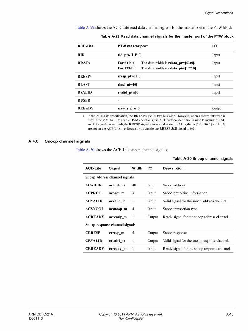
Signal Descriptions
Table A-29 shows the ACE-Lite read data channel signals for the master port of the PTW block.
A.4.6 Snoop channel signals
Table A-30 shows the ACE-Lite snoop channel signals.
Table A-29 Read data channel signals for the master port of the PTW block
ACE-Lite PTW master port I/O
RID rid_ptw[I_P:0] Input
RDATA For 64-bit The data width is rdata_ptw[63:0].For 128-bit The data width is rdata_ptw[127:0].
Input
RRESPa
a. In the ACE-Lite specification, the RRESP signal is two bits wide. However, when a shared interface is used in the MMU-401 to enable DVM operations, the ACE protocol definition is used to include the AC and CR signals. As a result, the RRESP signal is increased in size by 2 bits, that is [3:0]. Bit[3] and bit[2] are not on the ACE-Lite interfaces, so you can tie the RRESP[3:2] signal to 0x0.
rresp_ptw[1:0] Input
RLAST rlast_ptw[0] Input
RVALID rvalid_ptw[0] Input
RUSER - -
RREADY rready_ptw[0] Output
Table A-30 Snoop channel signals
ACE-Lite Signal Width I/O Description
Snoop address channel signals
ACADDR acaddr_m 40 Input Snoop address.
ACPROT acprot_m 3 Input Snoop protection information.
ACVALID acvalid_m 1 Input Valid signal for the snoop address channel.
ACSNOOP acsnoop_m 4 Input Snoop transaction type.
ACREADY acready_m 1 Output Ready signal for the snoop address channel.
Snoop response channel signals
CRRESP crresp_m 5 Output Snoop response.
CRVALID crvalid_m 1 Output Valid signal for the snoop response channel.
CRREADY crready_m 1 Input Ready signal for the snoop response channel.
ARM DDI 0521A Copyright © 2013 ARM. All rights reserved. A-16ID051113 Non-Confidential
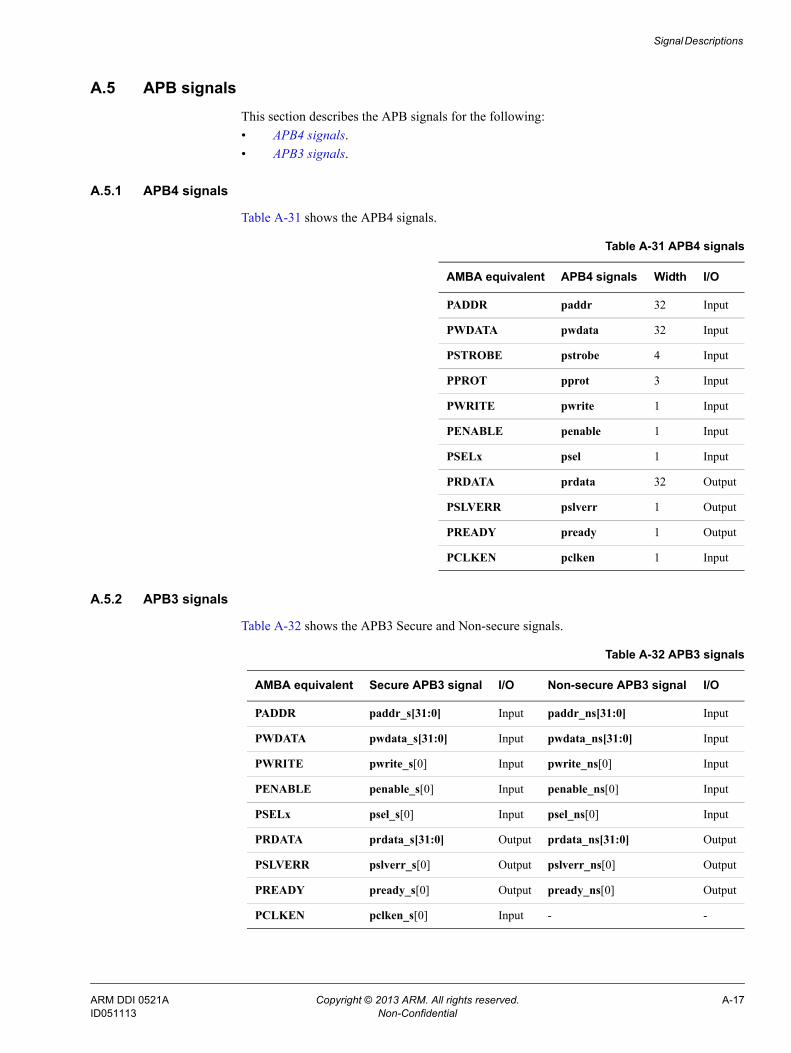
Signal Descriptions
A.5 APB signals This section describes the APB signals for the following:• APB4 signals.• APB3 signals.
A.5.1 APB4 signals
Table A-31 shows the APB4 signals.
A.5.2 APB3 signals
Table A-32 shows the APB3 Secure and Non-secure signals.
Table A-31 APB4 signals
AMBA equivalent APB4 signals Width I/O
PADDR paddr 32 Input
PWDATA pwdata 32 Input
PSTROBE pstrobe 4 Input
PPROT pprot 3 Input
PWRITE pwrite 1 Input
PENABLE penable 1 Input
PSELx psel 1 Input
PRDATA prdata 32 Output
PSLVERR pslverr 1 Output
PREADY pready 1 Output
PCLKEN pclken 1 Input
Table A-32 APB3 signals
AMBA equivalent Secure APB3 signal I/O Non-secure APB3 signal I/O
PADDR paddr_s[31:0] Input paddr_ns[31:0] Input
PWDATA pwdata_s[31:0] Input pwdata_ns[31:0] Input
PWRITE pwrite_s[0] Input pwrite_ns[0] Input
PENABLE penable_s[0] Input penable_ns[0] Input
PSELx psel_s[0] Input psel_ns[0] Input
PRDATA prdata_s[31:0] Output prdata_ns[31:0] Output
PSLVERR pslverr_s[0] Output pslverr_ns[0] Output
PREADY pready_s[0] Output pready_ns[0] Output
PCLKEN pclken_s[0] Input - -
ARM DDI 0521A Copyright © 2013 ARM. All rights reserved. A-17ID051113 Non-Confidential
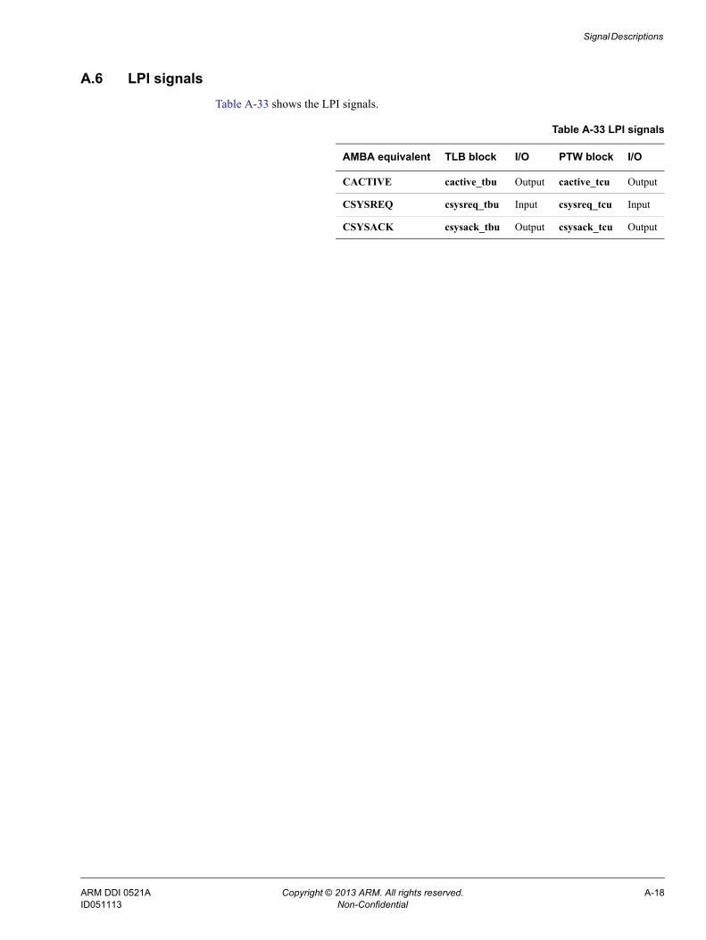
Signal Descriptions
A.6 LPI signalsTable A-33 shows the LPI signals.
Table A-33 LPI signals
AMBA equivalent TLB block I/O PTW block I/O
CACTIVE cactive_tbu Output cactive_tcu Output
CSYSREQ csysreq_tbu Input csysreq_tcu Input
CSYSACK csysack_tbu Output csysack_tcu Output
ARM DDI 0521A Copyright © 2013 ARM. All rights reserved. A-18ID051113 Non-Confidential

Signal Descriptions
A.7 Miscellaneous signalsThis section describes the non-AMBA signals as follows:• Sideband signals.• Interrupt signals.• MBIST signals on page A-20.• Authentication interface signal on page A-20.• Tie-off signals on page A-20.• Performance event signals on page A-21.
A.7.1 Sideband signals
Table A-34 shows the sideband signals.
A.7.2 Interrupt signals
Table A-35 shows the interrupt signals generated from the MMU-401. See the ARM System Memory Management Unit Architecture Specification for more information.
Table A-34 Sideband signals
Signal I/O Width Description
rsb_ns Input 1 Determines the Non-secure state of an incoming read transaction. The value of this signal can change with value of the arvalid signal.
wsb_ns Input 1 Determines the Non-secure state of an incoming write transaction. The value of this signal can change with the value of the awvalid signal.
wsb_ssd Input 0-15 Indicates the SSD index. If the rsb_ns or wsb_ns signal exists, then this signal does not exist. The value of this signal can change with the value of the awvalid signal.
rsb_ssd Input 0-15 Indicates the SSD index. If the rsb_ns or wsb_ns signal exists, then this signal does not exist. The value of this signal can change with the value of the arvalid signal.
wsb_sid_s Input 1-15 Indicate the write stream ID. The value of this signal can change with the value of the awvalid signal.
rsb_sid_s Input 1-15 Sideband signal to indicate the read stream ID. The value of this signal can change with the value of the arvalid signal.
Table A-35 Interrupt signals
Signal I/O Width Description
cfg_flt_irpt_s Output 1 Secure configuration access fault interrupt.
cfg_flt_irpt_ns Output 1 Non-secure configuration access fault interrupt.
glbl_flt_irpt_s Output 1 Global Secure fault interrupt.
glbl_flt_irpt_ns Output 1 Global Non-secure fault interrupt.
prf_irpt Output 1 Performance interrupt.
cxt_irpt_ns Output 1 Non-secure context interrupt.
comb_irpt_ns Output 1 Non-secure combined interrupt.
comb_irpt_s Output 1 Secure combined interrupt.
ARM DDI 0521A Copyright © 2013 ARM. All rights reserved. A-19ID051113 Non-Confidential

Signal Descriptions
A.7.3 MBIST signals
The MMU-401 supports a standard ARM MBIST interface to ensure that timing is met after inserting an MBIST multiplexer. You must not insert any MBIST multiplexers. This interface exists only when the RAM option is selected for the TLB data. See the CoreLink MMU-401 System Memory Management Unit Implementation Guide for more information.
Table A-36 shows the MBIST signals.
A.7.4 Authentication interface signal
The authentication interface disables AXI accesses. Table A-37 shows the authentication interface signal. See the CoreSight Architecture Specification for more information.
A.7.5 Tie-off signals
Table A-38 shows the tie-off signals.
Table A-36 MBIST signals
Signal I/O Width Description
mbistreq Input 1 MBIST request from the MBIST controller to the TLB RAM.
mbistack Output 1 Acknowlegement from the MMU-401 that it is ready for an MBIST operation.
mbistaddr Input TLB_INDEX_WIDTHa-1:0 Right-justified address. This address is same as the physical address of the memory.
mbistreaden Input 1 Read enable.
mbistwriteen Input 1 Write enable.
mbistindata Input 52 Write data.
mbistoutdata Output 52 Read data, that is valid for three clocks after read enable is set.
a. Where, TLB_INDEX_WIDTH is equal to log 2TLB depth.
Table A-37 Authentication interface signal
Signal I/O Width Description
spniden Input 1 Secure privileged Non-invasive debug enable. When the spniden signal is high, it enables the counting of Secure events.The options are as follows:0b0 Secure events are not counted as part of performance counters.0b1 Secure events are counted as part of performance counters.
Table A-38 Tie-off signals
Signal I/O Width Description
cfg_cttw Input - Static configuration to indicate whether the MMU-401 performs coherent page table walks. The value of this signal cannot change after reset.
testmode Input 1 When this signal is high, the DFT mode is enabled within the design. The options are as follows:0b0 Functional mode.0b1 Test mode.
ARM DDI 0521A Copyright © 2013 ARM. All rights reserved. A-20ID051113 Non-Confidential
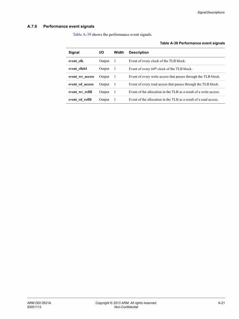
Signal Descriptions
A.7.6 Performance event signals
Table A-39 shows the performance event signals.
Table A-39 Performance event signals
Signal I/O Width Description
event_clk Output 1 Event of every clock of the TLB block.
event_clk64 Output 1 Event of every 64th clock of the TLB block.
event_wr_access Output 1 Event of every write access that passes through the TLB block.
event_rd_access Output 1 Event of every read access that passes through the TLB block.
event_wr_refill Output 1 Event of the allocation in the TLB as a result of a write access.
event_rd_refill Output 1 Event of the allocation in the TLB as a result of a read access.
ARM DDI 0521A Copyright © 2013 ARM. All rights reserved. A-21ID051113 Non-Confidential

ARM DDI 0521A Copyright © 2013 ARM. All rights reserved. B-1ID051113 Non-Confidential
Appendix B Revisions
This appendix describes the technical changes between released issues of this book.
Table B-1 Issue A
Change Location Affects
No changes, first release - -


