RF Power Field Effect TransistorsHigh Ruggedness N--ChannelEnhancement--Mode Lateral MOSFETsThese high ruggedness devices are designed for use in high VSWR industrial
(including laser and plasma exciters), broadcast (analog and digital), aerospaceand radio/land mobile applications. They are unmatched input and outputdesigns allowing wide frequency range utilization, between 1.8 and 600 MHz.• Typical Performance: VDD = 50 Volts, IDQ = 100 mA
Signal TypePout(W)
f(MHz)
Gps(dB)
ηD(%)
IRL(dB)
Pulsed (100 μsec,20% Duty Cycle)
300 Peak 230 26.5 74.0 --16
CW 300 Avg. 130 25.0 80.0 --15
• Capable of Handling a Load Mismatch of 65:1 VSWR, @ 50 Vdc, 230 MHz,at all Phase Angles• 300 Watts CW Output Power• 300 Watts Pulsed Peak Power, 20% Duty Cycle, 100 μsec
• Capable of 300 Watts CW OperationFeatures• Unmatched Input and Output Allowing Wide Frequency Range Utilization• Device can be used Single--Ended or in a Push--Pull Configuration• Qualified Up to a Maximum of 50 VDD Operation• Characterized from 30 V to 50 V for Extended Power Range• Suitable for Linear Application with Appropriate Biasing• Integrated ESD Protection• Greater Negative Gate--Source Voltage Range for Improved Class C Operation• Characterized with Series Equivalent Large--Signal Impedance Parameters• RoHS Compliant• NI--780--4 in Tape and Reel. R3 Suffix = 250 Units, 56 mm Tape Width,
13 inch Reel. For R5 Tape and Reel options, see p. 14.• NI--780S--4 in Tape and Reel. R3 Suffix = 250 Units, 32 mm Tape Width,
13 inch Reel. For R5 Tape and Reel options, see p. 14.
Table 1. Maximum Ratings
Rating Symbol Value Unit
Drain--Source Voltage VDSS --0.5, +130 Vdc
Gate--Source Voltage VGS --6.0, +10 Vdc
Storage Temperature Range Tstg --65 to +150 °C
Case Operating Temperature TC 150 °C
Total Device Dissipation @ TC = 25°CDerate above 25°C
PD 10505.26
WW/°C
Operating Junction Temperature (1,2) TJ 225 °C
Table 2. Thermal Characteristics
Characteristic Symbol Value (2,3) Unit
Thermal Resistance, Junction to Case (4)
Pulsed: Case Temperature 75°C, 300 W Pulsed, 100 μsec Pulse Width, 20% Duty Cycle,50 Vdc, IDQ = 100 mA, 230 MHz
CW: Case Temperature 87°C, 300 W CW, 50 Vdc, IDQ = 1100 mA, 230 MHzZθJCRθJC
0.050.19
°C/W
1. Continuous use at maximum temperature will affect MTTF.2. MTTF calculator available at http://www.freescale.com/rf. Select Software & Tools/Development Tools/Calculators to access
MTTF calculators by product.3. Refer to AN1955, Thermal Measurement Methodology of RF Power Amplifiers. Go to http://www.freescale.com/rf.
Select Documentation/Application Notes -- AN1955.4. Same test circuit is used for both pulsed and CW.
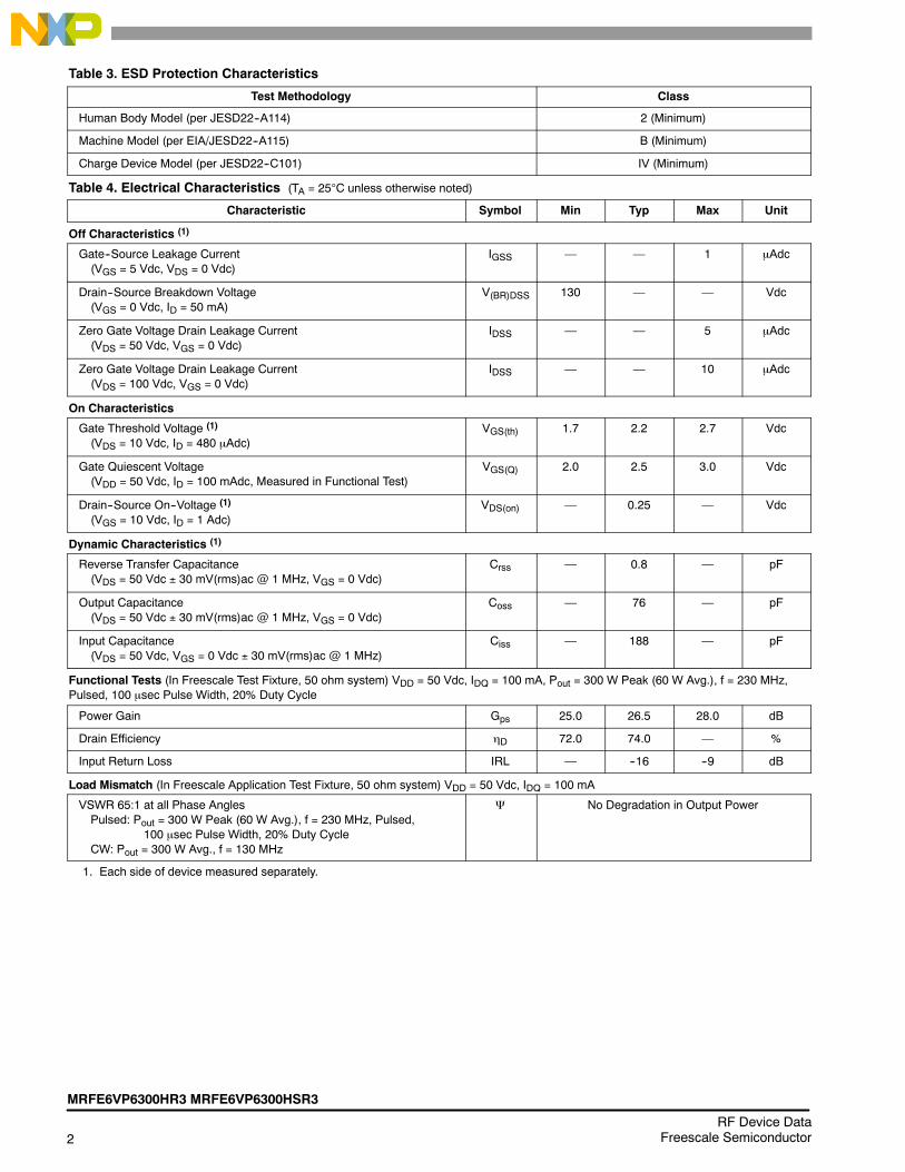
Functional Tests (In Freescale Test Fixture, 50 ohm system) VDD = 50 Vdc, IDQ = 100 mA, Pout = 300 W Peak (60 W Avg.), f = 230 MHz,Pulsed, 100 μsec Pulse Width, 20% Duty Cycle
Power Gain Gps 25.0 26.5 28.0 dB
Drain Efficiency ηD 72.0 74.0 %
Input Return Loss IRL --16 --9 dB
Load Mismatch (In Freescale Application Test Fixture, 50 ohm system) VDD = 50 Vdc, IDQ = 100 mA
VSWR 65:1 at all Phase AnglesPulsed: Pout = 300 W Peak (60 W Avg.), f = 230 MHz, Pulsed,
100 μsec Pulse Width, 20% Duty CycleCW: Pout = 300 W Avg., f = 130 MHz
Ψ No Degradation in Output Power
1. Each side of device measured separately.
MRFE6VP6300HR3 MRFE6VP6300HSR3
3RF Device DataFreescale Semiconductor
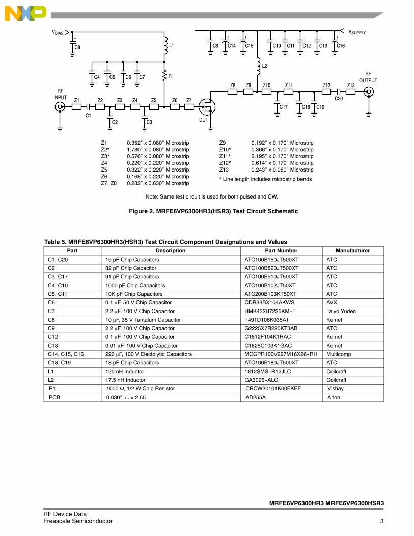
Figure 2. MRFE6VP6300HR3(HSR3) Test Circuit Schematic
Z9 0.192″ x 0.170″ MicrostripZ10* 0.366″ x 0.170″ MicrostripZ11* 2.195″ x 0.170″ MicrostripZ12* 0.614″ x 0.170″ MicrostripZ13 0.243″ x 0.080″ Microstrip
* Line length includes microstrip bends
Z1 0.352″ x 0.080″ MicrostripZ2* 1.780″ x 0.080″ MicrostripZ3* 0.576″ x 0.080″ MicrostripZ4 0.220″ x 0.220″ MicrostripZ5 0.322″ x 0.220″ MicrostripZ6 0.168″ x 0.220″ MicrostripZ7, Z8 0.282″ x 0.630″ Microstrip
Z1
RFINPUT
C1
Z2 Z4
DUT
C20
RFOUTPUT
VBIAS VSUPPLY
C5
C9 C11C14
+
Z12
Z3
C15
+
Z5
C6
Z11Z10Z9Z8
Z7Z6
R1C4
Z13
C12C8
+L1
C7
C3C2
C19C18C17
L2
C16
+
C10 C13
Note: Same test circuit is used for both pulsed and CW.
Table 5. MRFE6VP6300HR3(HSR3) Test Circuit Component Designations and ValuesPart Description Part Number Manufacturer
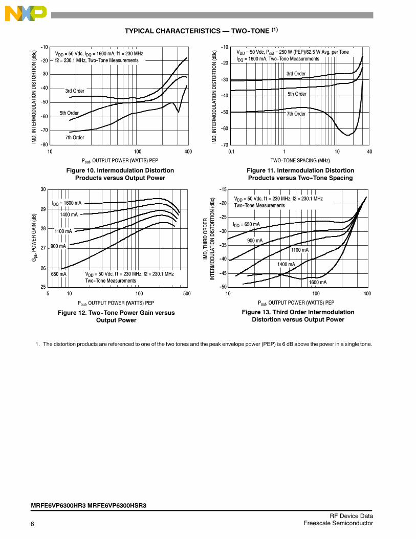
VDD = 50 Vdc, Pout = 250 W (PEP)/62.5 W Avg. per ToneIDQ = 1600 mA, Two--Tone Measurements
--35
--30
--60
29
27
1400 mA
--20
10 100
650 mA
1100 mA
900 mA
--20
100
IDQ = 650 mA
1400 mA
1100 mA
900 mA
1600 mA
1. The distortion products are referenced to one of the two tones and the peak envelope power (PEP) is 6 dB above the power in a single tone.
MRFE6VP6300HR3 MRFE6VP6300HSR3
7RF Device DataFreescale Semiconductor
TYPICAL CHARACTERISTICS
250
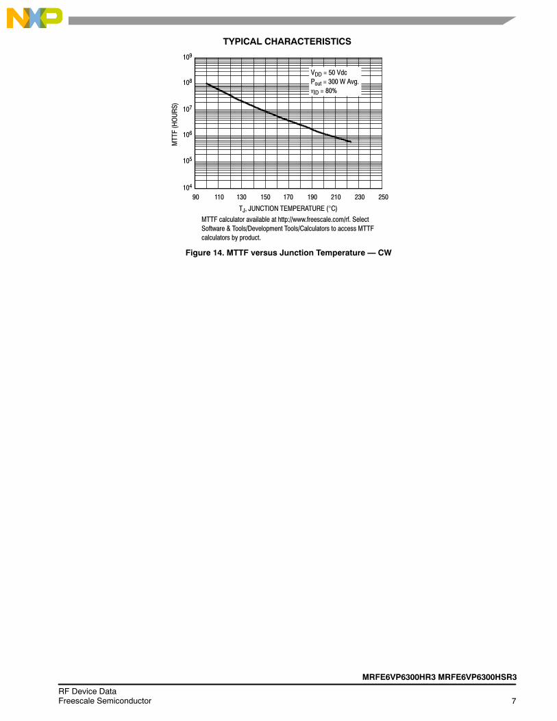
109
90
TJ, JUNCTION TEMPERATURE (°C)
Figure 14. MTTF versus Junction Temperature CW
MTTF calculator available at http://www.freescale.com/rf. SelectSoftware & Tools/Development Tools/Calculators to access MTTFcalculators by product.
107
106
104
110 130 150 170 190
MTTF(HOURS)
210 230
108
105
VDD = 50 VdcPout = 300 W Avg.ηD = 80%
8RF Device Data
Freescale Semiconductor
MRFE6VP6300HR3 MRFE6VP6300HSR3
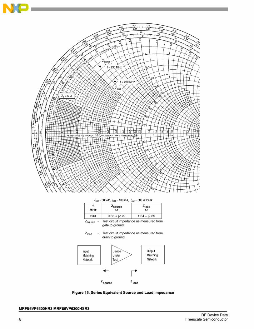
f = 230 MHz
f = 230 MHz
Zload
Zsource
Zo = 5Ω
VDD = 50 Vdc, IDQ = 100 mA, Pout = 300 W Peak
fMHz
ZsourceΩ
ZloadΩ
230 0.65 + j2.79 1.64 + j2.85
Zsource = Test circuit impedance as measured fromgate to ground.
Zload = Test circuit impedance as measured fromdrain to ground.
Figure 15. Series Equivalent Source and Load Impedance
Zsource Z load
InputMatchingNetwork
DeviceUnderTest
OutputMatchingNetwork
MRFE6VP6300HR3 MRFE6VP6300HSR3
9RF Device DataFreescale Semiconductor
VDD = 50 Vdc, IDQ = 100 mA
fMHz
ZsourceΩ
ZloadΩ
10 36.0 + j128 12.0 + j8.80
25 20.0 + j64.0 12.4 + j6.40
50 16.0 + j41.6 11.6 + j14.4
100 8.00 + j24.8 9.00 + j9.80
200 3.00 + j12.8 7.20 + j6.40
300 1.52 + j7.92 6.00 + j5.00
400 1.08 + j5.04 4.20 + j4.00
500 1.04 + j3.16 3.32 + j2.72
600 0.88 + j1.76 2.72 + j1.68
1. Simulated performance at 1 dB gain compression.
Zsource = Source impedance presented from gate to gate.
Zload = Load impedance presented from drain to drain.
LoadSource
Figure 16. Simulated Source and Load Impedances Optimized for IRL,Output Power and Drain Efficiency Push--Pull
Zsource Z load
DeviceUnderTest
--
-- +
+
10RF Device Data
Freescale Semiconductor
MRFE6VP6300HR3 MRFE6VP6300HSR3
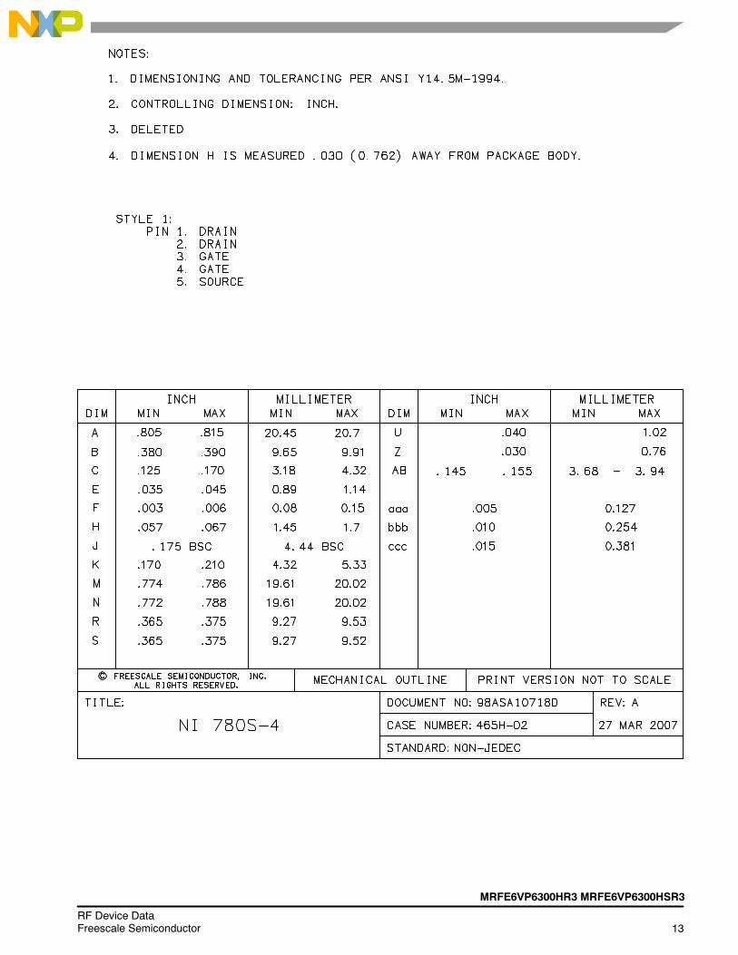
PACKAGE DIMENSIONS
MRFE6VP6300HR3 MRFE6VP6300HSR3
11RF Device DataFreescale Semiconductor
12RF Device Data
Freescale Semiconductor
MRFE6VP6300HR3 MRFE6VP6300HSR3
MRFE6VP6300HR3 MRFE6VP6300HSR3
13RF Device DataFreescale Semiconductor
14RF Device Data
Freescale Semiconductor
MRFE6VP6300HR3 MRFE6VP6300HSR3
PRODUCT DOCUMENTATION AND SOFTWARE
Refer to the following documents to aid your design process.
Application Notes• AN1955: Thermal Measurement Methodology of RF Power Amplifiers
Engineering Bulletins• EB212: Using Data Sheet Impedances for RF LDMOS Devices
Software• Electromigration MTTF Calculator
• RF High Power Model
• .s2p File
For Software, do a Part Number search at http://www.freescale.com, and select the Part Number link. Go to the Software &Tools tab on the parts Product Summary page to download the respective tool.
R5 TAPE AND REEL OPTION
NI--780--4 = R5 Suffix = 50 Units, 56 mm Tape Width, 13 inch Reel.NI--780S--4 = R5 Suffix = 50 Units, 32 mm Tape Width, 13 inch Reel.
The R5 tape and reel option for MRFE6VP6300H and MRFE6VP6300HS parts will be available for 2 years after release ofMRFE6VP6300H and MRFE6VP6300HS. Freescale Semiconductor, Inc. reserves the right to limit the quantities that will bedelivered in the R5 tape and reel option. At the end of the 2 year period customers who have purchased these devices in the R5tape and reel option will be offered MRFE6VP6300H and MRFE6VP6300HS in the R3 tape and reel option.
REVISION HISTORY
The following table summarizes revisions to this document.
Revision Date Description
0 Oct. 2010 • Initial Release of Data Sheet
1 July 2011 • Corrected pin 4 label from RFout/VGS to RFin/VGS, Fig. 1, Pin Connections, p. 1
• Changed Drain--Source voltage from --0.5, +125 to --0.5, +130 in Maximum Ratings table, p. 1
• Added Total Device Dissipation to Maximum Ratings table, p. 1
• Changed V(BR)DSS Min value from 125 to 130 Vdc, Table 4, Off Characteristics, p. 2
• Tightened VGS(th) Min limit from 1.5 to 1.7 Vdc and Max limit from 3.0 to 2.7 Vdc as a result of processimprovement, Table 4, On Characteristics, p. 2
• Tightened VGS(Q) Min limit from 1.7 to 2.0 Vdc and Max limit from 3.2 to 3.0 Vdc as a result of processimprovement, Table 4, On Characteristics, p. 2
• Added Load Mismatch table to Table 4. Electrical Characteristics, p. 2
• MTTF end temperature on graph changed to match maximum operating junction temperature, Fig. 14,MTTF versus Junction Temperature, p. 7
• Added Fig. 16, Simulated Source and Load Impedances Optimized for IRL, Output Power and DrainEfficiency Push--Pull table, p. 9
MRFE6VP6300HR3 MRFE6VP6300HSR3
15RF Device DataFreescale Semiconductor
Information in this document is provided solely to enable system and softwareimplementers to use Freescale Semiconductor products. There are no express orimplied copyright licenses granted hereunder to design or fabricate any integratedcircuits or integrated circuits based on the information in this document.
Freescale Semiconductor reserves the right to make changes without further notice toany products herein. Freescale Semiconductor makes no warranty, representation orguarantee regarding the suitability of its products for any particular purpose, nor doesFreescale Semiconductor assume any liability arising out of the application or use ofany product or circuit, and specifically disclaims any and all liability, including withoutlimitation consequential or incidental damages. Typical parameters that may beprovided in Freescale Semiconductor data sheets and/or specifications can and dovary in different applications and actual performance may vary over time. All operatingparameters, including Typicals, must be validated for each customer application bycustomers technical experts. Freescale Semiconductor does not convey any licenseunder its patent rights nor the rights of others. Freescale Semiconductor products arenot designed, intended, or authorized for use as components in systems intended forsurgical implant into the body, or other applications intended to support or sustain life,or for any other application in which the failure of the Freescale Semiconductor productcould create a situation where personal injury or death may occur. Should Buyerpurchase or use Freescale Semiconductor products for any such unintended orunauthorized application, Buyer shall indemnify and hold Freescale Semiconductorand its officers, employees, subsidiaries, affiliates, and distributors harmless against allclaims, costs, damages, and expenses, and reasonable attorney fees arising out of,directly or indirectly, any claim of personal injury or death associated with suchunintended or unauthorized use, even if such claim alleges that FreescaleSemiconductor was negligent regarding the design or manufacture of the part.
USA/Europe or Locations Not Listed:Freescale Semiconductor, Inc.Technical Information Center, EL5162100 East Elliot RoadTempe, Arizona 852841--800--521--6274 or +1--480--768--2130www.freescale.com/support
Europe, Middle East, and Africa:Freescale Halbleiter Deutschland GmbHTechnical Information CenterSchatzbogen 781829 Muenchen, Germany+44 1296 380 456 (English)+46 8 52200080 (English)+49 89 92103 559 (German)+33 1 69 35 48 48 (French)www.freescale.com/support
Japan:Freescale Semiconductor Japan Ltd.HeadquartersARCO Tower 15F1--8--1, Shimo--Meguro, Meguro--ku,Tokyo 153--0064Japan0120 191014 or +81 3 5437 [email protected]
Asia/Pacific:Freescale Semiconductor China Ltd.Exchange Building 23FNo. 118 Jianguo RoadChaoyang DistrictBeijing 100022China+86 10 5879 [email protected]
For Literature Requests Only:Freescale Semiconductor Literature Distribution Center1--800--441--2447 or +1--303--675--2140Fax: [email protected]