+ All Categories
Home > Documents > Document Number: MW6S004N Technical Data Rev. 4, 6/2009 … · RF Power Field Effect Transistor ......

Document Number: MW6S004N Technical Data Rev. 4, 6/2009 … · RF Power Field Effect Transistor ......

Date post: 14-May-2018
Category:
Upload: doankhuong
View: 213 times
Download: 0 times
Share this document with a friend
13
RF Power Field Effect Transistor N - Channel Enhancement - Mode Lateral MOSFET Designed for Class A or Class AB base station applications with frequencies up to 2000 MHz. Suitable for analog and digital modulation and multicarrier amplifier applications. Typical Two-Tone Performance @ 1960 MHz, 28 Volts, I DQ = 50 mA, P out = 4 Watts PEP Power Gain 18 dB Drain Efficiency 33% IMD - 34 dBc Typical Two-Tone Performance @ 900 MHz, 28 Volts, I DQ = 50 mA, P out = 4 Watts PEP Power Gain 19 dB Drain Efficiency 33% IMD - 39 dBc Capable of Handling 5:1 VSWR, @ 28 Vdc, 1960 MHz, 4 Watts CW Output Power Features Characterized with Series Equivalent Large - Signal Impedance Parameters On - Chip RF Feedback for Broadband Stability Integrated ESD Protection RoHS Compliant In Tape and Reel. T1 Suffix = 1000 Units per 12 mm, 7 inch Reel. Table 1. Maximum Ratings Rating Symbol Value Unit Drain-Source Voltage V DSS - 0.5, +68 Vdc Gate-Source Voltage V GS - 0.5, +12 Vdc Storage Temperature Range T stg - 65 to +150 °C Operating Junction Temperature T J 150 °C Table 2. Thermal Characteristics Characteristic Symbol Value (1,2) Unit Thermal Resistance, Junction to Case Case Temperature 76°C, 4 W PEP, Two-Tone Case Temperature 79°C, 4 W CW R θJC 8.8 8.5 °C/W Table 3. ESD Protection Characteristics Test Methodology Class Human Body Model (per JESD22-A114) 1C (Minimum) Machine Model (per EIA/JESD22-A115) A (Minimum) Charge Device Model (per JESD22 - C101) IV (Minimum) 1. MTTF calculator available at http://www.freescale.com/rf . Select Software & Tools/Development Tools/Calculators to access MTTF calculators by product. 2. Refer to AN1955, Thermal Measurement Methodology of RF Power Amplifiers. Go to http://www.freescale.com/rf . Select Documentation/Application Notes - AN1955. Document Number: MW6S004N Rev. 4, 6/2009 Freescale Semiconductor Technical Data MW6S004NT1 1 - 2000 MHz, 4 W, 28 V LATERAL N-CHANNEL RF POWER MOSFET CASE 466 - 03, STYLE 1 PLD 1.5 PLASTIC © Freescale Semiconductor, Inc., 2007, 2009. All rights reserved.
Transcript

MW6S004NT1

1RF Device DataFreescale Semiconductor

RF Power Field Effect TransistorN-Channel Enhancement-Mode Lateral MOSFET

Designed for Class A or Class AB base station applications with frequenciesup to 2000 MHz. Suitable for analog and digital modulation and multicarrieramplifier applications.

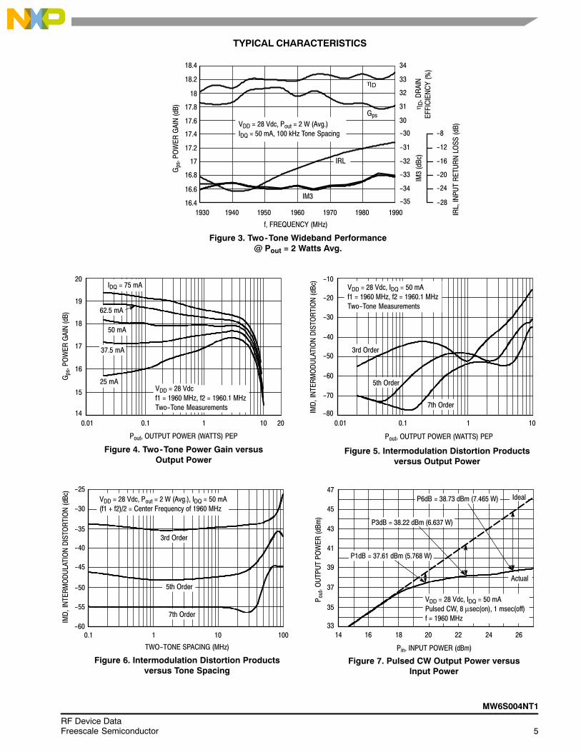
• Typical Two-Tone Performance @ 1960 MHz, 28 Volts, IDQ = 50 mA, Pout = 4 Watts PEP

Power Gain � 18 dBDrain Efficiency � 33%IMD � -34 dBc

• Typical Two-Tone Performance @ 900 MHz, 28 Volts, IDQ = 50 mA, Pout = 4 Watts PEP

Power Gain � 19 dBDrain Efficiency � 33%IMD � -39 dBc

• Capable of Handling 5:1 VSWR, @ 28 Vdc, 1960 MHz, 4 Watts CW OutputPower

Features

• Characterized with Series Equivalent Large-Signal Impedance Parameters

• On-Chip RF Feedback for Broadband Stability• Integrated ESD Protection• RoHS Compliant• In Tape and Reel. T1 Suffix = 1000 Units per 12 mm, 7 inch Reel.

Table 1. Maximum Ratings

Rating Symbol Value Unit

Drain-Source Voltage VDSS -0.5, +68 Vdc

Gate-Source Voltage VGS -0.5, +12 Vdc

Storage Temperature Range Tstg - 65 to +150 °C

Operating Junction Temperature TJ 150 °C

Table 2. Thermal Characteristics

Characteristic Symbol Value (1,2) Unit

Thermal Resistance, Junction to CaseCase Temperature 76°C, 4 W PEP, Two-ToneCase Temperature 79°C, 4 W CW

RθJC8.88.5

°C/W

Table 3. ESD Protection Characteristics

Test Methodology Class

Human Body Model (per JESD22-A114) 1C (Minimum)

Machine Model (per EIA/JESD22-A115) A (Minimum)

Charge Device Model (per JESD22-C101) IV (Minimum)

1. MTTF calculator available at http://www.freescale.com/rf. Select Software & Tools/Development Tools/Calculators to access MTTF calculators by product.

2. Refer to AN1955, Thermal Measurement Methodology of RF Power Amplifiers. Go to http://www.freescale.com/rf. Select Documentation/Application Notes - AN1955.

Document Number: MW6S004NRev. 4, 6/2009

Freescale SemiconductorTechnical Data

MW6S004NT1

1-2000 MHz, 4 W, 28 VLATERAL N-CHANNEL

RF POWER MOSFET

CASE 466-03, STYLE 1PLD 1.5

PLASTIC

© Freescale Semiconductor, Inc., 2007, 2009. All rights reserved.

2RF Device Data

Freescale Semiconductor

MW6S004NT1

Table 4. Moisture Sensitivity Level

Test Methodology Rating Package Peak Temperature Unit

Per JESD 22-A113, IPC/JEDEC J-STD-020 3 260 °C

Table 5. Electrical Characteristics (TA = 25°C unless otherwise noted)

Characteristic Symbol Min Typ Max Unit

Off Characteristics

Zero Gate Voltage Drain Leakage Current(VDS = 68 Vdc, VGS = 0 Vdc)

IDSS � � 10 μAdc

Zero Gate Voltage Drain Leakage Current(VDS = 28 Vdc, VGS = 0 Vdc)

IDSS � � 10 μAdc

Gate-Source Leakage Current(VGS = 5 Vdc, VDS = 0 Vdc)

IGSS � � 500 nAdc

On Characteristics

Gate Threshold Voltage(VDS = 10 Vdc, ID = 50 mAdc)

VGS(th) 1.2 2 2.7 Vdc

Gate Quiescent Voltage(VDS = 28 Vdc, ID = 50 mAdc)

VGS(Q) � 2.7 � Vdc

Fixture Gate Quiescent Voltage (1)

(VDD = 28 Vdc, ID = 50 mAdc, Measured in Functional Test)VGG(Q) 2.2 3 4.2 Vdc

Drain-Source On-Voltage(VGS = 10 Vdc, ID = 50 mAdc)

VDS(on) � 0.27 0.37 Vdc

Dynamic Characteristics

Reverse Transfer Capacitance(VDS = 28 Vdc ± 30 mV(rms)ac @ 1 MHz, VGS = 0 Vdc)

Crss � 21 � pF

Output Capacitance(VDS = 28 Vdc ± 30 mV(rms)ac @ 1 MHz, VGS = 0 Vdc)

Coss � 25 � pF

Input Capacitance(VDS = 28 Vdc, VGS = 0 Vdc ± 30 mV(rms)ac @ 1 MHz)

Ciss � 30 � pF

Functional Tests (In Freescale Test Fixture, 50 ohm system) VDD = 28 Vdc, IDQ = 50 mA, Pout = 4 W PEP, f1 = 1960 MHz, f2 = 1960.1 MHz, Two-Tone Test

Power Gain Gps 16.5 18 20 dB

Drain Efficiency ηD 28 33 � %

Intermodulation Distortion IMD � -34 -28 dBc

Input Return Loss IRL � -12 -10 dB

Typical Performance (In Freescale 900 MHz Demo Board, 50 ohm system) VDD = 28 Vdc, IDQ = 50 mA, Pout = 4 W PEP, f = 900 MHz, Two-Tone Test, 100 kHz Tone Spacing

Power Gain Gps � 19 � dB

Drain Efficiency ηD � 33 � %

Intermodulation Distortion IMD � -39 � dBc

Input Return Loss IRL � -12 � dB

1. VGG = 11/10 x VGS(Q). Parameter measured on Freescale Test Fixture, due to resistive divider network on the board. Refer to Test Circuit Schematic.

MW6S004NT1

3RF Device DataFreescale Semiconductor

Figure 1. MW6S004NT1 Test Circuit Schematic

Z7 0.210″ x 1.220″ MicrostripZ8 0.054″ x 0.680″ MicrostripZ9 0.054″ x 0.260″ MicrostripZ10 0.025″ x 0.930″ MicrostripPCB Arlon CuClad 250GX-0300-55-22, 0.020″, εr = 2.5

Z1 0.054″ x 0.430″ MicrostripZ2 0.054″ x 0.137″ MicrostripZ3 0.580″ x 0.420″ MicrostripZ4 0.580″ x 0.100″ MicrostripZ5 0.025″ x 0.680″ MicrostripZ6 0.210″ x 0.100″ Microstrip

RF

OUTPUT

VBIASVSUPPLY

RF

INPUT

DUT

Z1

C2

R1

C8

+

C1 C7R2 Z5

R3

Z2 Z3 Z4

Z6

Z10

C3 C4 C5

Z7 Z8

C6

Z9

Table 6. MW6S004NT1 Test Circuit Component Designations and Values

Part Description Part Number Manufacturer

C1 100 nF Chip Capacitor CDR33BX104AKYS Kemet

C2, C3, C6, C7 9.1 pF Chip Capacitors ATC100B9R1CT500XT ATC

C4, C5 10 μF, 50 V Chip Capacitors GRM55DR61H106KA88B Murata

C8 10 μF, 35 V Tantalum Chip Capacitor T490D106K035AT Kemet

R1 1 kΩ, 1/4 W Chip Resistor CRCW12061001FKEA Vishay

R2 10 kΩ, 1/4 W Chip Resistor CRCW12061002FKEA Vishay

R3 10 Ω, 1/4 W Chip Resistor CRCW120610R0FKEA Vishay

4RF Device Data

Freescale Semiconductor

MW6S004NT1

Figure 2. MW6S004NT1 Test Circuit Component Layout

25

C8

MW6S004N

Rev 3

R1 C1R2C7

C2 R3

C3C4 C5

C6

MW6S004NT1

5RF Device DataFreescale Semiconductor

TYPICAL CHARACTERISTICS

Gps

, PO

WE

R G

AIN

(dB

)

IRL,

IN

PU

T R

ET

UR

N L

OS

S (

dB)

IM3

(dB

c)

−28

−16

−20

−24

19901930

IRL

Gps

f, FREQUENCY (MHz)

Figure 3. Two-Tone Wideband Performance@ Pout = 2 Watts Avg.

19801970196019501940

18.4

18.2

−35

34

33

32

−31

−33

η D,

DR

AIN

EF

FIC

IEN

CY

(%

)

ηD18

17.8

17.6

17.2

16.4

16.8

17.4

−32

−30

31

−12

IM3

Pout, OUTPUT POWER (WATTS) PEP

14

20

1

IDQ = 75 mA

19

17

16

10 20

Figure 4. Two-Tone Power Gain versusOutput Power

10

−80

−10

0.01

7th Order

VDD = 28 Vdc, IDQ = 50 mA

f1 = 1960 MHz, f2 = 1960.1 MHz

Two−Tone Measurements

5th Order

3rd Order

1

−20

−30

−40

−50

−60

Pout, OUTPUT POWER (WATTS) PEP

Figure 5. Intermodulation Distortion Productsversus Output Power

IMD

, IN

TE

RM

OD

ULA

TIO

N D

IST

OR

TIO

N (

dBc)

Gps

, PO

WE

R G

AIN

(dB

)

10−60

−25

0.1

7th Order

TWO−TONE SPACING (MHz)

5th Order

3rd Order

−30

−35

−40

−45

−50

1 100

Figure 6. Intermodulation Distortion Productsversus Tone Spacing

26

47

P3dB = 38.22 dBm (6.637 W)

Pin, INPUT POWER (dBm)

VDD = 28 Vdc, IDQ = 50 mA

Pulsed CW, 8 μsec(on), 1 msec(off)

f = 1960 MHz

43

41

37

35

33

16 18 22

Actual

Ideal

2414

Figure 7. Pulsed CW Output Power versusInput Power

IMD

, IN

TE

RM

OD

ULA

TIO

N D

IST

OR

TIO

N (

dBc)

Pou

t, O

UT

PU

T P

OW

ER

(dB

m)

1850 mA

62.5 mA

P1dB = 37.61 dBm (5.768 W)

−55

0.01

VDD = 28 Vdc, Pout = 2 W (Avg.)

IDQ = 50 mA, 100 kHz Tone Spacing

17

16.6

30

−34

−8

15

0.1

VDD = 28 Vdc

f1 = 1960 MHz, f2 = 1960.1 MHz

Two−Tone Measurements

37.5 mA

25 mA

−70

0.1

VDD = 28 Vdc, Pout = 2 W (Avg.), IDQ = 50 mA

(f1 + f2)/2 = Center Frequency of 1960 MHz 45

39

20

P6dB = 38.73 dBm (7.465 W)

6RF Device Data

Freescale Semiconductor

MW6S004NT1

TYPICAL CHARACTERISTICS

AC

PR

(dB

)

0 −70

Pout, OUTPUT POWER (WATTS) AVG.

50 −20

40 −30

30 −40

20 −50

10 −60

0.01 1 10

Gps

ACPR

Figure 8. Single-Carrier CDMA ACPR, Power Gainand Drain Efficiency versus Output Power

10

14

20

0.01

0

60

TC = −30�C

25�C

−30�C

1

19

18

17

16

40

30

20

10

Pout, OUTPUT POWER (WATTS) CW

Figure 9. Power Gain and Drain Efficiencyversus CW Output Power

Gps

, PO

WE

R G

AIN

(dB

)

Gps

Pout, OUTPUT POWER (WATTS) CW

Figure 10. Power Gain versus Output Power

IDQ = 50 mA

f = 1960 MHz

VDD = 24 V

715

19

0 6

17

16

18

2 3 4

Gps

, PO

WE

R G

AIN

(dB

)

12

22

1800

−25

0

S21

f, FREQUENCY (MHz)

Figure 11. Broadband Frequency Response

S11

20 −5

18

16

−10

−15

14 −20

210020502000195019001850

VDD = 28 Vdc

Pout = 2 W CW

IDQ = 50 mA

S11

(dB

)

S21

(dB

)

85�C

85�C

851

VDD = 28 Vdc

IDQ = 50 mA

f = 1960 MHz

28 V 32 V

ηD

η D, D

RA

IN E

FF

ICIE

NC

Y (

%),

Gps

, PO

WE

R G

AIN

(dB

)

η D, D

RA

IN E

FF

ICIE

NC

Y (

%)

0.1

VDD = 28 Vdc, IDQ = 50 mA

f = 1960 MHz, N−CDMA IS−95 (Pilot, Sync,

Paging, Traffic Codes 8 Through 13)

15

0.1

50

ηD

18.5

17.5

16.5

15.5

MW6S004NT1

7RF Device DataFreescale Semiconductor

TYPICAL CHARACTERISTICS

250

107

90

TJ, JUNCTION TEMPERATURE (°C)

Figure 12. MTTF versus Junction Temperature

This above graph displays calculated MTTF in hours when the device

is operated at VDD = 28 Vdc, Pout = 4 W PEP, and ηD = 33%.

MTTF calculator available at http://www.freescale.com/rf. Select

Software & Tools/Development Tools/Calculators to access MTTF

calculators by product.

106

105

104

110 130 150 170 190

MT

TF

(H

OU

RS

)

210 230

8RF Device Data

Freescale Semiconductor

MW6S004NT1

f = 1930 MHz

Zo = 10 ΩZload

Zsourcef = 1990 MHz

f = 1930 MHz

f = 1990 MHz

VDD = 28 Vdc, IDQ = 50 mA, Pout = 4 W PEP

fMHz

Zsource�

Zload�

1930 1.96 - j5.34 8.78 + j6.96

1960 1.89 - j5.10 8.93 + j7.46

1990 1.82 - j4.85 9.11 + j7.97

Zsource = Test circuit impedance as measured from gate to ground.

Zload = Test circuit impedance as measured fromdrain to ground.

Zsource

Zload

Input

Matching

Network

Device

Under

Test

Output

Matching

Network

Figure 13. Series Equivalent Source and Load Impedance

MW6S004NT1

9RF Device DataFreescale Semiconductor

Table 7. Common Source Scattering Parameters (VDD = 28 V, 50 ohm system)

IDQ = 50 mA

fMH

S11 S21 S12 S22MHz

|S11| ∠ φ |S21| ∠ φ |S12| ∠ φ |S22| ∠ φ

500 0.649 -116.340 7.902 105.420 0.056 -73.750 0.548 -33.570

550 0.695 -121.680 7.502 98.790 0.053 -80.570 0.593 -41.480

600 0.733 -126.560 7.111 92.380 0.049 -87.010 0.632 -48.890

650 0.770 -131.340 6.699 86.290 0.045 -93.280 0.669 -56.000

700 0.800 -135.740 6.302 80.450 0.041 -99.120 0.701 -62.810

750 0.827 -140.030 5.922 74.850 0.038 -104.850 0.727 -69.290

800 0.848 -143.950 5.552 69.630 0.035 -110.110 0.750 -75.350

850 0.866 -147.690 5.220 64.580 0.032 -115.220 0.770 -81.130

900 0.882 -151.140 4.891 59.970 0.029 -119.960 0.786 -86.570

950 0.895 -154.560 4.597 55.490 0.026 -124.790 0.800 -91.730

1000 0.907 -157.590 4.315 51.240 0.024 -129.090 0.813 -96.660

1050 0.916 -160.540 4.060 47.170 0.022 -133.370 0.824 -101.340

1100 0.923 -163.310 3.819 43.340 0.020 -137.460 0.833 -105.790

1150 0.929 -165.930 3.601 39.650 0.018 -141.440 0.840 -110.050

1200 0.935 -168.430 3.398 36.110 0.017 -145.330 0.847 -114.170

1250 0.938 -170.770 3.210 32.740 0.015 -149.540 0.851 -118.060

1300 0.942 -173.030 3.036 29.490 0.014 -153.430 0.856 -121.880

1350 0.945 -175.140 2.875 26.360 0.013 -157.460 0.859 -125.520

1400 0.948 -177.170 2.728 23.330 0.012 -161.910 0.863 -129.020

1450 0.951 -179.090 2.590 20.440 0.011 -166.180 0.866 -132.390

1500 0.953 179.030 2.464 17.640 0.010 -170.630 0.869 -135.650

1550 0.954 177.270 2.347 14.920 0.009 -174.890 0.872 -138.760

1600 0.955 175.570 2.240 12.320 0.008 179.950 0.875 -141.750

1650 0.956 173.980 2.139 9.740 0.008 173.920 0.877 -144.650

1700 0.957 172.350 2.047 7.250 0.007 167.710 0.880 -147.480

1750 0.957 170.800 1.958 4.810 0.007 161.810 0.882 -150.180

1800 0.958 169.340 1.879 2.440 0.006 155.370 0.884 -152.760

1850 0.959 167.920 1.806 0.260 0.006 148.940 0.886 -155.230

1900 0.959 166.510 1.736 -1.980 0.005 142.630 0.887 -157.580

1950 0.960 165.200 1.668 -4.310 0.005 136.740 0.888 -160.050

2000 0.959 163.800 1.611 -6.240 0.005 129.910 0.890 -162.070

2050 0.959 162.420 1.555 -8.290 0.005 123.810 0.891 -164.190

2100 0.958 161.170 1.504 -10.270 0.005 118.200 0.892 -166.140

2150 0.958 159.840 1.456 -12.210 0.005 112.740 0.893 -168.060

2200 0.957 158.560 1.412 -14.130 0.005 108.460 0.894 -169.840

2250 0.957 157.160 1.372 -16.010 0.005 103.840 0.896 -171.610

2300 0.955 155.870 1.334 -17.870 0.005 99.310 0.896 -173.260

2350 0.954 154.510 1.300 -19.700 0.005 95.360 0.897 -174.830

2400 0.953 153.120 1.268 -21.510 0.005 91.030 0.898 -176.390

2450 0.953 151.730 1.238 -23.250 0.005 87.460 0.899 -177.840

10RF Device Data

Freescale Semiconductor

MW6S004NT1

Table 7. Common Source Scattering Parameters (VDD = 28 V, 50 ohm system) (continued)

IDQ = 50 mA

fMH

S11 S21 S12 S22MHz

|S11| ∠ φ |S21| ∠ φ |S12| ∠ φ |S22| ∠ φ

2500 0.952 150.340 1.211 -25.120 0.006 84.160 0.899 -179.270

2550 0.950 149.010 1.187 -26.920 0.006 80.780 0.897 179.420

2600 0.949 147.380 1.166 -28.650 0.006 77.880 0.897 178.120

2650 0.948 145.920 1.144 -30.420 0.007 74.670 0.898 176.840

2700 0.944 144.200 1.121 -32.310 0.007 71.360 0.896 175.480

2750 0.944 142.790 1.105 -34.230 0.007 67.980 0.897 174.060

2800 0.943 141.020 1.088 -36.000 0.007 63.950 0.897 172.930

2850 0.941 139.410 1.073 -37.870 0.007 61.230 0.896 171.630

2900 0.940 137.640 1.058 -39.760 0.008 59.810 0.896 170.330

2950 0.938 135.900 1.045 -41.680 0.008 58.280 0.896 169.040

3000 0.937 133.860 1.032 -43.610 0.008 56.740 0.895 167.510

MW6S004NT1

11RF Device DataFreescale Semiconductor

PACKAGE DIMENSIONS

CASE 466-03ISSUE D

NOTES:1. INTERPRET DIMENSIONS AND TOLERANCES

PER ASME Y14.5M, 1984.2. CONTROLLING DIMENSION: INCH3. RESIN BLEED/FLASH ALLOWABLE IN ZONE V, W,

AND X.

DIM MIN MAX MIN MAX

MILLIMETERSINCHES

A 0.255 0.265 6.48 6.73

B 0.225 0.235 5.72 5.97

C 0.065 0.072 1.65 1.83

D 0.130 0.150 3.30 3.81

E 0.021 0.026 0.53 0.66

F 0.026 0.044 0.66 1.12

G 0.050 0.070 1.27 1.78

H 0.045 0.063 1.14 1.60

K 0.273 0.285 6.93 7.24

L 0.245 0.255 6.22 6.48

N 0.230 0.240 5.84 6.10

P 0.000 0.008 0.00 0.20

Q 0.055 0.063 1.40 1.60

R 0.200 0.210 5.08 5.33

S 0.006 0.012 0.15 0.31

U 0.006 0.012 0.15 0.31

ZONE V 0.000 0.021 0.00 0.53

ZONE W 0.000 0.010 0.00 0.25

ZONE X 0.000 0.010 0.00 0.25

STYLE 1:PIN 1. DRAIN

2. GATE 3. SOURCE 4. SOURCE

J 0.160 0.180 4.06 4.57ÉÉÉÉÉÉÉÉÉÉÉÉÉÉÉ

ÉÉÉÉÉÉÉÉÉÉÉÉÉÉÉ

ÉÉÉÉÉÉÉÉÉÉ

A

B D

F

LR

3

4

21

KN

ZONE V

ZONE W

ZONE XGS

HU

�10 DRAFT

P

CE

0.35 (0.89) X 45 5�

Y Y

Q

VIEW Y-Y

� �

4

21

3

PLASTICPLD 1.5

12RF Device Data

Freescale Semiconductor

MW6S004NT1

PRODUCT DOCUMENTATION, TOOLS AND SOFTWARE

Refer to the following documents to aid your design process.

Application Notes

• AN1955: Thermal Measurement Methodology of RF Power Amplifiers

Engineering Bulletins• EB212: Using Data Sheet Impedances for RF LDMOS Devices

Software

• Electromigration MTTF Calculator

• RF High Power Model

For Software and Tools, do a Part Number search at http://www.freescale.com, and select the �Part Number� link. Go to theSoftware & Tools tab on the part�s Product Summary page to download the respective tool.

REVISION HISTORY

The following table summarizes revisions to this document.

Revision Date Description

2 Feb. 2007 • Corrected MSL Rating from 3 to 1 in Table 4, Moisture Sensitivity Level, p. 2

• Updated VGS(th) and VGS(Q) to reflect tighter HV6 windows and added Fixture Gate Quiescent VGG(Q) to OnCharacteristics table to account for test fixture resistor divider network, p. 2

• Updated Part Numbers in Table 6, Component Designations and Values, to RoHS compliant partnumbers, p. 3

• Removed lower voltage tests from Fig. 10, Power Gain versus Output Power, due to fixed tuned fixturelimitations, p. 6

• Replaced Figure 12, MTTF versus Junction Temperature with updated graph. Removed Amps2 and listedoperating characteristics and location of MTTF calculator for device, p. 7

• Added Product Documentation and Revision History section, p. 12

3 Apr. 2009 • Corrected ESD structures to reflect current testing results. Changed HBM from 1A to 1C and CDM from IIIto IV, p. 1

• Corrected Ciss test condition to indicate AC stimulus on the VGS connection versus the VDS connection,Dynamic Characteristics table, p. 2

• Updated PCB information to show more specific material details, Fig. 1, Test Circuit Schematic, p. 3

• Updated Part Numbers in Table 6, Component Designations and Values, to latest RoHS compliant partnumbers, p. 3

4 June 2009 • Modified data sheet to reflect MSL rating change from 1 to 3 as a result of the standardization of packingprocess as described in Product and Process Change Notification number, PCN13516, p. 2

• Added Electromigration MTTF Calculator and RF High Power Model availability to Product Documentation,Tools and Software, p. 12

MW6S004NT1

13RF Device DataFreescale Semiconductor

Information in this document is provided solely to enable system and softwareimplementers to use Freescale Semiconductor products. There are no express orimplied copyright licenses granted hereunder to design or fabricate any integratedcircuits or integrated circuits based on the information in this document.

Freescale Semiconductor reserves the right to make changes without further notice toany products herein. Freescale Semiconductor makes no warranty, representation orguarantee regarding the suitability of its products for any particular purpose, nor doesFreescale Semiconductor assume any liability arising out of the application or use ofany product or circuit, and specifically disclaims any and all liability, including withoutlimitation consequential or incidental damages. �Typical� parameters that may beprovided in Freescale Semiconductor data sheets and/or specifications can and dovary in different applications and actual performance may vary over time. All operatingparameters, including �Typicals�, must be validated for each customer application bycustomer�s technical experts. Freescale Semiconductor does not convey any licenseunder its patent rights nor the rights of others. Freescale Semiconductor products arenot designed, intended, or authorized for use as components in systems intended forsurgical implant into the body, or other applications intended to support or sustain life,or for any other application in which the failure of the Freescale Semiconductor productcould create a situation where personal injury or death may occur. Should Buyerpurchase or use Freescale Semiconductor products for any such unintended orunauthorized application, Buyer shall indemnify and hold Freescale Semiconductorand its officers, employees, subsidiaries, affiliates, and distributors harmless against allclaims, costs, damages, and expenses, and reasonable attorney fees arising out of,directly or indirectly, any claim of personal injury or death associated with suchunintended or unauthorized use, even if such claim alleges that FreescaleSemiconductor was negligent regarding the design or manufacture of the part.

Freescale� and the Freescale logo are trademarks of Freescale Semiconductor, Inc.All other product or service names are the property of their respective owners.© Freescale Semiconductor, Inc. 2007, 2009. All rights reserved.

How to Reach Us:

Home Page:www.freescale.com

Web Support:http://www.freescale.com/support

USA/Europe or Locations Not Listed:Freescale Semiconductor, Inc.Technical Information Center, EL5162100 East Elliot RoadTempe, Arizona 852841-800-521-6274 or +1-480-768-2130www.freescale.com/support

Europe, Middle East, and Africa:Freescale Halbleiter Deutschland GmbHTechnical Information CenterSchatzbogen 781829 Muenchen, Germany+44 1296 380 456 (English)+46 8 52200080 (English)+49 89 92103 559 (German)+33 1 69 35 48 48 (French)www.freescale.com/support

Japan:Freescale Semiconductor Japan Ltd.HeadquartersARCO Tower 15F1-8-1, Shimo-Meguro, Meguro-ku,Tokyo 153-0064Japan0120 191014 or +81 3 5437 [email protected]

Asia/Pacific:Freescale Semiconductor China Ltd.Exchange Building 23FNo. 118 Jianguo RoadChaoyang DistrictBeijing 100022 China +86 10 5879 [email protected]

For Literature Requests Only:Freescale Semiconductor Literature Distribution Center1-800-441-2447 or +1-303-675-2140Fax: [email protected]

Document Number: MW6S004NRev. 4, 6/2009


Recommended