The MW7IC2040N wideband integrated circuit is designed with on-chipmatching that makes it usable from 1805 to 1990 MHz. This multi -stagestructure is rated for 24 to 32 Volt operation and covers all typical cellular basestation modulation formats.
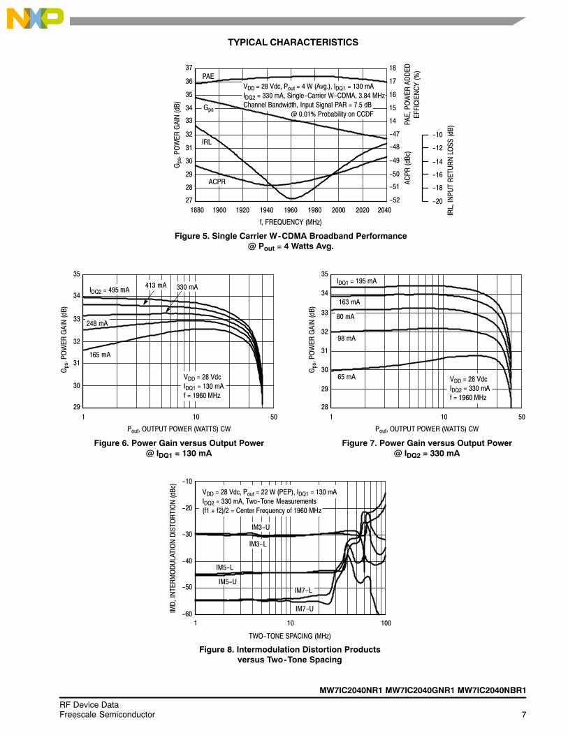
• Typical Single-Carrier W-CDMA Performance: VDD = 28 Volts, IDQ1 =130 mA, IDQ2 = 330 mA, Pout = 4 Watts Avg., f = 1932.5, ChannelBandwidth = 3.84 MHz, Input Signal PAR = 7.5 dB @ 0.01% Probabilityon CCDF.
Power Gain � 32 dBPower Added Efficiency � 17.5%ACPR @ 5 MHz Offset � -50 dBc in 3.84 MHz Bandwidth
• Capable of Handling 5:1 VSWR, @ 32 Vdc, 1960 MHz, 50 Watts CW Output Power (3 dB Input Overdrive from Rated Pout)
• Stable into a 3:1 VSWR. All Spurs Below -60 dBc @ 100 mW to 40 WattsCW Pout.
• Typical Pout @ 1 dB Compression Point � 30 Watts CWGSM EDGE Application• Typical GSM EDGE Performance: VDD = 28 Volts, IDQ1 = 90 mA, IDQ2 =
Pout = 40 Watts CW, 1805-1880 MHz and 1930-1990 MHzPower Gain � 31 dBPower Added Efficiency � 50%
Features• Characterized with Series Equivalent Large-Signal Impedance Parameters
and Common Source S-Parameters• On-Chip Matching (50 Ohm Input, DC Blocked, >3 Ohm Output)• Integrated Quiescent Current Temperature Compensation with Enable/
Disable Function (1)
• Integrated ESD Protection• 225°C Capable Plastic Package• RoHS Compliant• In Tape and Reel. R1 Suffix = 500 Units per 44 mm, 13 inch Reel.
1. Refer to AN1977, Quiescent Current Thermal Tracking Circuit in the RF Integrated Circuit Family and to AN1987, Quiescent Current Controlfor the RF Integrated Circuit Device Family. Go to http://www.freescale.com/rf. Select Documentation/Application Notes - AN1977 or AN1987.
Document Number: MW7IC2040NRev. 1, 11/2009
Freescale SemiconductorTechnical Data
MW7IC2040NR1MW7IC2040GNR1MW7IC2040NBR1
1930-1990 MHz, 1805-1880 MHz,4 W AVG., 28 V
SINGLE W-CDMA, GSM EDGE, GSMRF LDMOS WIDEBAND
INTEGRATED POWER AMPLIFIERS
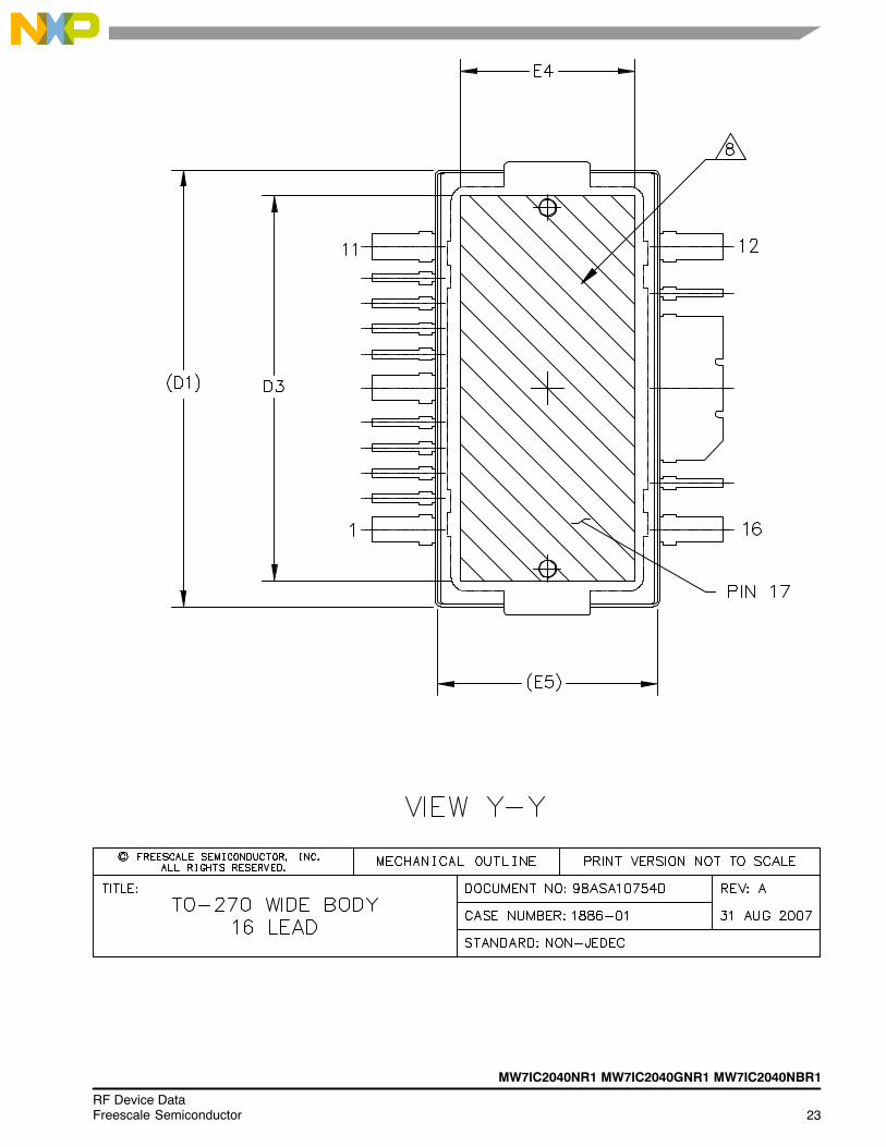
CASE 1886-01TO-270 WB-16
PLASTICMW7IC2040NR1
CASE 1887-01TO-270 WB-16 GULL
PLASTICMW7IC2040GNR1
CASE 1329-09TO-272 WB-16
PLASTICMW7IC2040NBR1
Figure 1. Functional Block Diagram
Quiescent Current
Temperature Compensation (1)
VDS1
RFin
VGS1
RFout/VDS2
VGS2
VDS1
(Top View)
GND
NC
RFin
VGS1
GNDVDS1
RFout/VDS2
GND
VGS2VDS1
GND
2345
6
78
16
15
14
1312
910
11
1
VGS2VGS1
NC
NC
NC
Figure 2. Pin Connections
Note: Exposed backside of the package isthe source terminal for the transistors.
1. Continuous use at maximum temperature will affect MTTF.2. MTTF calculator available at http://www.freescale.com/rf. Select Software & Tools/Development Tools/Calculators to access MTTF
calculators by product.3. Refer to AN1955, Thermal Measurement Methodology of RF Power Amplifiers. Go to http://www.freescale.com/rf.
IMD Symmetry @ 22 W PEP, Pout where IMD Third OrderIntermodulation � 30 dBc (Delta IMD Third Order Intermodulationbetween Upper and Lower Sidebands > 2 dB)
IMDsym� 60 �
MHz
VBW Resonance Point(IMD Third Order Intermodulation Inflection Point)
VBWres � 65 � MHz
Quiescent Current Accuracy over Temperature (2)
with 5.6 kΩ Gate Feed Resistors ( -30 to 85°C)ΔIQT � ±3 � %
Gain Flatness in 60 MHz Bandwidth @ Pout = 4 W Avg. GF � 1.2 � dB
Average Deviation from Linear Phase in 60 MHz Bandwidth@ Pout = 30 W CW
Φ � 0.5 � °
Average Group Delay @ Pout = 30 W CW, f = 1960 MHz Delay � 2.5 � ns
Part - to-Part Insertion Phase Variation @ Pout = 30 W CW,f = 1960 MHz, Six Sigma Window
ΔΦ � 33 � °
Gain Variation over Temperature(-30°C to +85°C)
ΔG � 0.029 � dB/°C
Output Power Variation over Temperature(-30°C to +85°C)
ΔP1dB � 0.003 � dBm/°C
1. Part internally matched both on input and output.2. Refer to AN1977, Quiescent Current Thermal Tracking Circuit in the RF Integrated Circuit Family and to AN1987, Quiescent Current Control
for the RF Integrated Circuit Device Family. Go to http://www.freescale.com/rf. Select Documentation/Application Notes - AN1977 orAN1987.
3. Measurement made with device in straight lead configuration before any lead forming operation is applied.(continued)
Typical CW Performance (In Freescale GSM EDGE 1930-1990 MHz Test Fixture, 50 ohm system) VDD = 28 Vdc, IDQ1 = 90 mA,IDQ2 = 430 mA, Pout = 40 W CW, 1805-1880 MHz and 1930-1990 MHz
Power Gain Gps � 31 � dB
Power Added Efficiency PAE � 50 � %
Input Return Loss IRL � -15 � dB
Pout @ 1 dB Compression Point P1dB � 45 � W
MW7IC2040NR1 MW7IC2040GNR1 MW7IC2040NBR1
5RF Device DataFreescale Semiconductor
Z10 0.3419″ x 0.1725″ MicrostripZ11 0.3419″ x 0.4671″ MicrostripZ12 0.0830″ x 0.4220″ MicrostripZ13, Z14 0.0830″ x 0.2855″ MicrostripZ15 0.0830″ x 0.9030″ MicrostripZ16 0.0830″ x 0.2499″ MicrostripPCB Rogers RO4350, 0.030″, εr = 3.5
Z1 0.0826″ x 0.5043″ MicrostripZ2 0.0826″ x 0.3639″ MicrostripZ3 0.0826″ x 0.4258″ MicrostripZ4 0.0826″ x 0.3639″ MicrostripZ5 0.0826″ x 0.3060″ MicrostripZ6 0.0826″ x 0.9290″ MicrostripZ7 0.0600″ x 0.1273″ MicrostripZ8, Z9 0.0800″ x 1.3684″ Microstrip
Figure 3. MW7IC2040NR1(GNR1)(NBR1) Test Circuit Schematic � 1930-1990 MHz
R1
RF
INPUT
VGG1
Z10
RF
OUTPUT
C5
C3
VDD2
1
2
3
4
5
6
7
8
14
13
1211
10
9
15
16DUT
Z6
C1
VDD1
Z8
Quiescent Current
Temperature
Compensation
Z1
Z9
Z11 Z12
C11
VGG2
C12 C10 C2
Z15
C17 C6
C13
+
C4 C18 C8 C9
Z7
C14
R2
C16
C15
Z16
Z13
C7
Z14
Z2
Z3
Z4Z5
NC
NCG1
G2
NC
NC
G2
G1
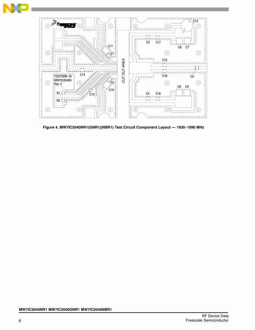
Table 6. MW7IC2040NR1(GNR1)(NBR1) Test Circuit Component Designations and Values � 1930-1990 MHzPart Description Part Number Manufacturer
Z8, Z9 0.0800″ x 1.1139″ MicrostripZ10 0.3419″ x 0.1725″ MicrostripZ11 0.3419″ x 0.4671″ MicrostripZ12 0.0830″ x 0.4220″ MicrostripZ13 0.0830″ x 0.9030″ MicrostripZ14 0.0830″ x 0.2499″ MicrostripPCB Rogers RO4350, 0.030″, εr = 3.5
Z1 0.0826″ x 0.5043″ MicrostripZ2 0.0826″ x 0.3639″ MicrostripZ3 0.0826″ x 0.4258″ MicrostripZ4 0.0826″ x 0.3639″ MicrostripZ5 0.0826″ x 0.3459″ MicrostripZ6 0.0826″ x 0.9115″ MicrostripZ7 0.0600″ x 0.1273″ Microstrip
Figure 18. MW7IC2040NR1(GNR1)(NBR1) Test Circuit Schematic � 1805-1880 MHz
R1
RF
INPUT
VGG1
Z10
RF
OUTPUT
C5
C3
VDD2
1
2
3
4
5
6
7
8
14
13
1211
10
9
15
16DUT
Z6
C1
VDD1
Z8
Quiescent Current
Temperature
Compensation
Z1
Z9
Z11 Z12
C11
VGG2
C12 C10 C2
Z13
C6
C13
+
C4 C8 C9
Z7
C14
R2
C16
Z14
C7
Z2
Z3
Z4Z5
NC
NCG1
G2
NC
NC
G2
G1
C15
Table 8. MW7IC2040NR1(GNR1)(NBR1) Test Circuit Component Designations and Values � 1805-1880 MHzPart Description Part Number Manufacturer
R1, R2 5.6 KΩ, 1/4 W Chip Resistors CRCW12065601FKEA Vishay
14RF Device Data
Freescale Semiconductor
MW7IC2040NR1 MW7IC2040GNR1 MW7IC2040NBR1
W-CDMA � 1805-1880 MHz
Figure 19. MW7IC2040NR1(GNR1)(NBR1) Test Circuit Component Layout � 1805-1880 MHz
CU
T O
UT
AR
EA
C14
R1
R2
C12
C10
C2
C1
C11
C4
C8 C9
C16
C15
C5
C6 C7
C13
C3
MW7IC2040NRev. 2
TO272WB−16
MW7IC2040NR1 MW7IC2040GNR1 MW7IC2040NBR1
15RF Device DataFreescale Semiconductor
GSM EDGE � 1805-1880 MHz
Z8, Z9 0.0800″ x 1.3354″ MicrostripZ10 0.3419″ x 0.1725″ MicrostripZ11 0.3419″ x 0.4671″ MicrostripZ12 0.0830″ x 0.3575″ MicrostripZ13 0.0830″ x 0.9675″ MicrostripZ14 0.0830″ x 0.2499″ MicrostripPCB Rogers RO4350, 0.030″, εr = 3.5
Z1 0.0826″ x 0.5043″ MicrostripZ2 0.0826″ x 0.3639″ MicrostripZ3 0.0826″ x 0.4258″ MicrostripZ4 0.0826″ x 0.2315″ MicrostripZ5 0.0826″ x 0.1324″ MicrostripZ6 0.0826″ x 1.2574″ MicrostripZ7 0.0600″ x 0.1273″ Microstrip
Figure 20. MW7IC2040NR1(GNR1)(NBR1) Test Circuit Schematic � 1805-1880 MHz
R1
RF
INPUT
VGG1
Z10
RF
OUTPUT
C5
C3
VDD2
1
2
3
4
5
6
7
8
14
13
1211
10
9
15
16DUT
Z6
C1
VDD1
Z8
Quiescent Current
Temperature
Compensation
Z1
Z9
Z11 Z12
C11
VGG2
C12 C10 C2
Z13
C6
C13
+
C4 C8 C9
Z7
C14
R2
C16
Z14
C7Z2
Z3
Z4
NC
NCG1
G2
NC
NC
G2
G1
Z5 C15
Table 9. MW7IC2040NR1(GNR1)(NBR1) Test Circuit Component Designations and Values � 1805-1880 MHzPart Description Part Number Manufacturer
C12 2.2 μF, 16 V Chip Capacitor C1206C225K4RAC Kemet
C13 470 μF, 63 V Electrolytic Capacitor, Radial MCGPR63V477M13X26-RH Multicomp
C14 0.8 pF Chip Capacitor ATC100B0R8BT500XT ATC
C15 1 pF Chip Capacitor ATC100B1R0BT500XT ATC
C16 1.2 pF Chip Capacitor ATC100B1R2BT500XT ATC
R1, R2 5.6 KΩ, 1/4 W Chip Resistors CRCW12065601FKEA Vishay
16RF Device Data
Freescale Semiconductor
MW7IC2040NR1 MW7IC2040GNR1 MW7IC2040NBR1
GSM EDGE � 1805-1880 MHz
Figure 21. MW7IC2040NR1(GNR1)(NBR1) Test Circuit Component Layout � 1805-1880 MHz
CU
T O
UT
AR
EA
C14
R1
R2
C12
C10
C2
C1
C11
C4
C8 C9
C16
C15
C5
C6 C7
C13
C3
MW7IC2040NRev. 2
TO272WB−16
MW7IC2040NR1 MW7IC2040GNR1 MW7IC2040NBR1
17RF Device DataFreescale Semiconductor
GSM EDGE � 1930-1990 MHz
Z8, Z9 0.0800″ x 1.6274″ MicrostripZ10 0.3419″ x 0.1725″ MicrostripZ11 0.3419″ x 0.4671″ MicrostripZ12 0.0830″ x 0.4685″ MicrostripZ13 0.0830″ x 0.8565″ MicrostripZ14 0.0830″ x 0.2499″ MicrostripPCB Rogers RO4350, 0.030″, εr = 3.5
Z1 0.0826″ x 0.5043″ MicrostripZ2 0.0826″ x 0.3639″ MicrostripZ3 0.0826″ x 0.4258″ MicrostripZ4 0.0826″ x 0.3639″ MicrostripZ5 0.0826″ x 0.6544″ MicrostripZ6 0.0826″ x 0.6030″ MicrostripZ7 0.0600″ x 0.1273″ Microstrip
Figure 22. MW7IC2040NR1(GNR1)(NBR1) Test Circuit Schematic � 1930-1990 MHz
R1
RF
INPUT
VGG1
Z10
RF
OUTPUT
C5
C3
VDD2
1
2
3
4
5
6
7
8
14
13
1211
10
9
15
16DUT
Z6
C1
VDD1
Z8
Quiescent Current
Temperature
Compensation
Z1
Z9
Z11 Z12
C11
VGG2
C12 C10 C2
Z13
C6
C13
+
C4 C8 C9
Z7
C14
R2
C16
Z14
C7
Z2
Z3
Z4Z5
NC
NCG1
G2
NC
NC
G2
G1
C15
Table 10. MW7IC2040NR1(GNR1)(NBR1) Test Circuit Component Designations and Values � 1930-1990 MHzPart Description Part Number Manufacturer
R1, R2 5.6 KΩ, 1/4 W Chip Resistors CRCW12065601FKEA Vishay
18RF Device Data
Freescale Semiconductor
MW7IC2040NR1 MW7IC2040GNR1 MW7IC2040NBR1
GSM EDGE � 1930-1990 MHz
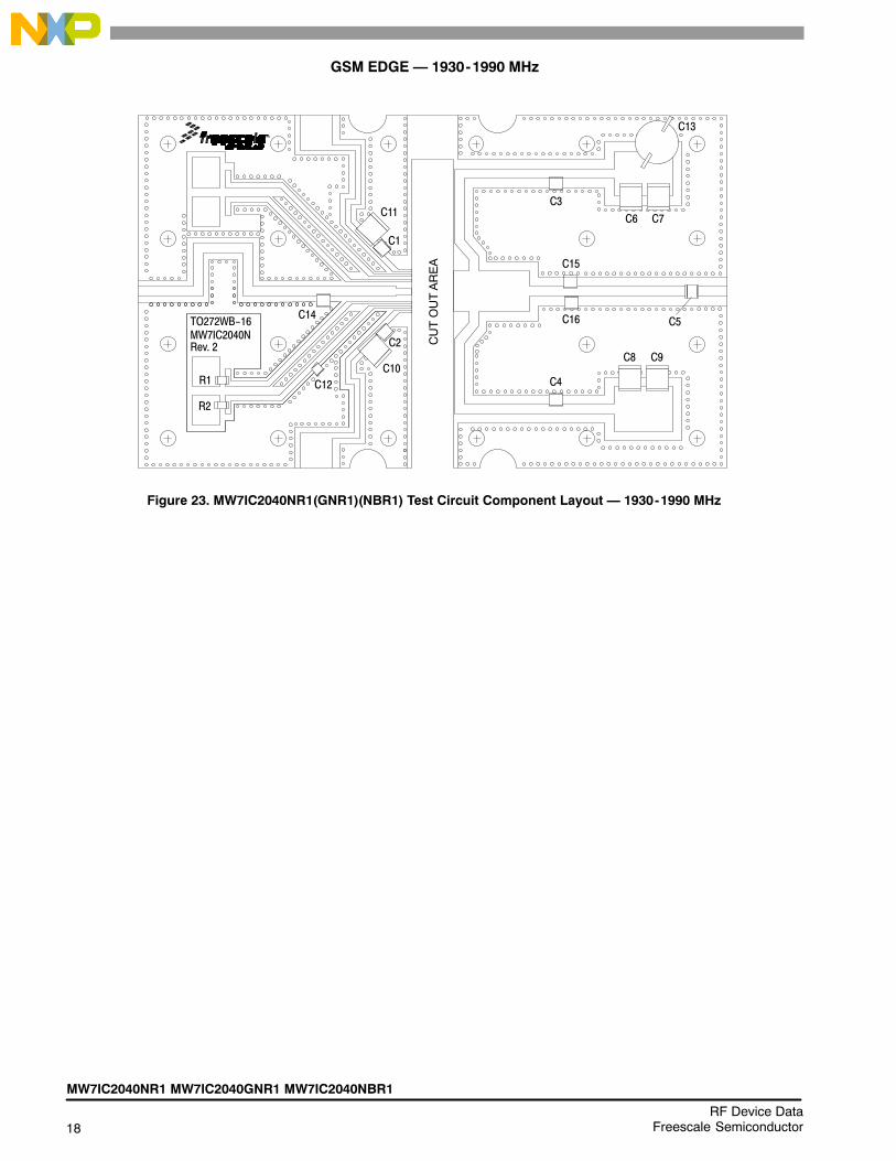
Figure 23. MW7IC2040NR1(GNR1)(NBR1) Test Circuit Component Layout � 1930-1990 MHz
CU
T O
UT
AR
EA
C14
R1
R2
C12
C10
C2
C1
C11
C4
C8 C9
C16
C15
C5
C6 C7
C13
C3
MW7IC2040NRev. 2
TO272WB−16
MW7IC2040NR1 MW7IC2040GNR1 MW7IC2040NBR1
19RF Device DataFreescale Semiconductor
PACKAGE DIMENSIONS
20RF Device Data
Freescale Semiconductor
MW7IC2040NR1 MW7IC2040GNR1 MW7IC2040NBR1
MW7IC2040NR1 MW7IC2040GNR1 MW7IC2040NBR1
21RF Device DataFreescale Semiconductor
22RF Device Data
Freescale Semiconductor
MW7IC2040NR1 MW7IC2040GNR1 MW7IC2040NBR1
MW7IC2040NR1 MW7IC2040GNR1 MW7IC2040NBR1
23RF Device DataFreescale Semiconductor
24RF Device Data
Freescale Semiconductor
MW7IC2040NR1 MW7IC2040GNR1 MW7IC2040NBR1
MW7IC2040NR1 MW7IC2040GNR1 MW7IC2040NBR1
25RF Device DataFreescale Semiconductor
26RF Device Data
Freescale Semiconductor
MW7IC2040NR1 MW7IC2040GNR1 MW7IC2040NBR1
MW7IC2040NR1 MW7IC2040GNR1 MW7IC2040NBR1
27RF Device DataFreescale Semiconductor
28RF Device Data
Freescale Semiconductor
MW7IC2040NR1 MW7IC2040GNR1 MW7IC2040NBR1
PRODUCT DOCUMENTATION, TOOLS AND SOFTWARE
Refer to the following documents to aid your design process.
Application Notes
• AN1907: Solder Reflow Attach Method for High Power RF Devices in Plastic Packages
• AN1955: Thermal Measurement Methodology of RF Power Amplifiers
• AN1977: Quiescent Current Thermal Tracking Circuit in the RF Integrated Circuit Family
• AN1987: Quiescent Current Control for the RF Integrated Circuit Device Family
• AN3263: Bolt Down Mounting Method for High Power RF Transistors and RFICs in Over-Molded Plastic Packages
• AN3789: Clamping of High Power RF Transistors and RFICs in Over-Molded Plastic Packages
Engineering Bulletins• EB212: Using Data Sheet Impedances for RF LDMOS Devices
Software• Electromigration MTTF Calculator
• RF High Power Model
For Software and Tools, do a Part Number search at http://www.freescale.com, and select the �Part Number� link. Go to theSoftware & Tools tab on the part�s Product Summary page to download the respective tool.
REVISION HISTORY
The following table summarizes revisions to this document.
Revision Date Description
0 Feb. 2009 • Initial Release of Data Sheet
1 Nov. 2009 • Updated Human Body Model ESD from Class 1C to 1B to reflect Human Body Model actual test data,p. 2
• Fig. 13, CCDF W-CDMA 3GPP, Test Model 1, 64 DPCH, 45.2% Clipping, Single-Carrier Test Signal andFig. 14, Single-Carrier W-CDMA Spectrum updated to show the undistorted input test signal, p. 9
• Added AN3789, Clamping of High Power RF Transistors and RFICs in Over-Molded Plastic Packages toProduct Documentation, Application Notes, p. 28
• Added Electromigration MTTF Calculator and RF High Power Model availability to Product Software,p. 28
MW7IC2040NR1 MW7IC2040GNR1 MW7IC2040NBR1
29RF Device DataFreescale Semiconductor
Information in this document is provided solely to enable system and softwareimplementers to use Freescale Semiconductor products. There are no express orimplied copyright licenses granted hereunder to design or fabricate any integratedcircuits or integrated circuits based on the information in this document.
Freescale Semiconductor reserves the right to make changes without further notice toany products herein. Freescale Semiconductor makes no warranty, representation orguarantee regarding the suitability of its products for any particular purpose, nor doesFreescale Semiconductor assume any liability arising out of the application or use ofany product or circuit, and specifically disclaims any and all liability, including withoutlimitation consequential or incidental damages. �Typical� parameters that may beprovided in Freescale Semiconductor data sheets and/or specifications can and dovary in different applications and actual performance may vary over time. All operatingparameters, including �Typicals�, must be validated for each customer application bycustomer�s technical experts. Freescale Semiconductor does not convey any licenseunder its patent rights nor the rights of others. Freescale Semiconductor products arenot designed, intended, or authorized for use as components in systems intended forsurgical implant into the body, or other applications intended to support or sustain life,or for any other application in which the failure of the Freescale Semiconductor productcould create a situation where personal injury or death may occur. Should Buyerpurchase or use Freescale Semiconductor products for any such unintended orunauthorized application, Buyer shall indemnify and hold Freescale Semiconductorand its officers, employees, subsidiaries, affiliates, and distributors harmless against allclaims, costs, damages, and expenses, and reasonable attorney fees arising out of,directly or indirectly, any claim of personal injury or death associated with suchunintended or unauthorized use, even if such claim alleges that FreescaleSemiconductor was negligent regarding the design or manufacture of the part.
USA/Europe or Locations Not Listed:Freescale Semiconductor, Inc.Technical Information Center, EL5162100 East Elliot RoadTempe, Arizona 852841-800-521-6274 or +1-480-768-2130www.freescale.com/support
Europe, Middle East, and Africa:Freescale Halbleiter Deutschland GmbHTechnical Information CenterSchatzbogen 781829 Muenchen, Germany+44 1296 380 456 (English)+46 8 52200080 (English)+49 89 92103 559 (German)+33 1 69 35 48 48 (French)www.freescale.com/support
Japan:Freescale Semiconductor Japan Ltd.HeadquartersARCO Tower 15F1-8-1, Shimo-Meguro, Meguro-ku,Tokyo 153-0064Japan0120 191014 or +81 3 5437 [email protected]
Asia/Pacific:Freescale Semiconductor China Ltd.Exchange Building 23FNo. 118 Jianguo RoadChaoyang DistrictBeijing 100022 China +86 10 5879 [email protected]
For Literature Requests Only:Freescale Semiconductor Literature Distribution Center1-800-441-2447 or +1-303-675-2140Fax: [email protected]