DOT/FAA/TC-16/40 Federal Aviation Administration William J. Hughes Technical Center Aviation Research Division Atlantic City International Airport New Jersey 08405 Commercial Off-the-Shelf Airborne Electronic Hardware Assurance Methods— Phase 3—Commodity Memories June 2017 Final Report This document is available to the U.S. public through the National Technical Information Services (NTIS), Springfield, Virginia 22161. This document is also available from the Federal Aviation Administration William J. Hughes Technical Center at actlibrary.tc.faa.gov. U.S. Department of Transportation Federal Aviation Administration
Transcript
DOT/FAA/TC-16/40
Federal Aviation Administration William J. Hughes Technical Center Aviation Research Division Atlantic City International Airport New Jersey 08405
This document is available to the U.S. public through the National Technical Information Services (NTIS), Springfield, Virginia 22161.
This document is also available from the Federal Aviation Administration William J. Hughes Technical Center at actlibrary.tc.faa.gov.
U.S. Department of Transportation Federal Aviation Administration
NOTICE
This document is disseminated under the sponsorship of the U.S. Department of Transportation in the interest of information exchange. The U.S. Government assumes no liability for the contents or use thereof. The U.S. Government does not endorse products or manufacturers. Trade or manufacturers’ names appear herein solely because they are considered essential to the objective of this report. The findings and conclusions in this report are those of the author(s) and do not necessarily represent the views of the funding agency. This document does not constitute FAA policy. Consult the FAA sponsoring organization listed on the Technical Documentation page as to its use. This report is available at the FAA William J. Hughes Technical Center’s Full-Text Technical Reports page: actlibrary.tc.faa.gov in Adobe Acrobat portable document format (PDF).
2. Government Accession No. 3. Recipient's Catalog No.
4. Title and Subtitle COMMERCIAL OFF-THE-SHELF AIRBORNE ELECTRONIC HARDWARE ASSURANCE METHODS—PHASE 3—COMMODITY
5. Report Date June 2017
MEMORIES 6. Performing Organization Code
7. Author(s) Laurence H. Mutuel, Vincent Brindejonc, Patrick Dervin
8. Performing Organization Report No. D8
9. Performing Organization Name and Address Thales Avionics, Inc.
10. Work Unit No. (TRAIS)
2733 South Crystal Drive, Suite 1200 Arlington, VA 22202
11. Contract or Grant No.
12. Sponsoring Agency Name and Address Federal Aviation Administration FAA National Headquarters 950 L’Enfant Plaza SW Washington, DC 20024
13. Type of Report and Period Covered Final Report November 2014 to November 2015 14. Sponsoring Agency Code AIR-134
15. Supplementary Notes The FAA William J. Hughes Technical Center Aviation Research Division Technical Monitors were Chakradhar Agava and Charles W. Kilgore, II (retired). 16. Abstract This report deals with the issue of using commodity memories in avionics, explains the reasons for the concern, and investigates methods used to ensure the reliability of the data stored in commodity memories. Because of the competitive nature regarding the efforts by manufacturers to produce devices that have vast numbers (i.e., millions and possibly billions) of these memories, their quality can be suspect, and their reliability and availability are likely to be less robust. Four types of commodity memories are covered in this report: double data rate, not-AND flash, toggle magnetoresistive, and quad data rate. This report provides a brief description of the technologies, manufacturing aspects, and defect management of these memories. Confidence in commodity memories is built not only from matching their type to the domain usage in the design phase but also by actively engaging with the commodity manufacturer and distributor. For the selected commodity memories, failure modes and failure mechanisms are discussed to illustrate the concern. Failure modes in commodity memories are described by using both a black-box and a grey-box model view and applying three levels of abstraction: functional, logical, and physical. Ensuring the reliability of these commodity memories is investigated through the existing fault mitigation techniques embedded in these memories and the identification of additional internal or external fault mitigation techniques. Error correcting codes are the typical built-in mitigation technique for each of the selected commodity memory types. Issues with built-in mitigation techniques typically point to a lack of documentation or poor coverage of the Airborne Electronic Hardware usage domain. Finally, the report presents a series of recommendations to support assurance of commodity memories in avionics products. 17. Key Words Commercial off-the-shelf, Commodity memory, Double data rate, Quad data rate, Magnetoresistive random access memory, Static random access memory, Not-AND flash memories, Supply chain, Failure mode, Error correcting code, Error detection and correction, Airborne electronic hardware, Redundancy, Memory test
18. Distribution Statement This document is available to the U.S. public through the National Technical Information Service (NTIS), Springfield, Virginia 22161. This document is also available from the Federal Aviation Administration William J. Hughes Technical Center at actlibrary.tc.faa.gov.
19. Security Classif. (of this report) Unclassified
20. Security Classif. (of this page) Unclassified
21. No. of Pages 115
22. Price
Form DOT F 1700.7 (8-72) Reproduction of completed page authorized
iii
ACKNOWLEDGEMENTS
The research that led to this report was coordinated with the technical experts and reviewers at Thales Avionics SAS by Cyril Marchand. Didier Regis and Guy Berthon acted as internal reviewers for this report.
iv
TABLE OF CONTENTS
Page
EXECUTIVE SUMMARY x
1. INTRODUCTION 1
1.1 Background 1 1.2 Purpose 2
2. IDENTIFICATION OF COMMODITY MEMORIES FOR AEH PURPOSES 2
2.1 Problem statement 2 2.2 Selected Types of Commodity Memories 3
2.2.1 Double Data Rate Synchronous Dynamic Random Access Memories 3 2.2.2 Not-AND Flash Memories 5 2.2.3 Quad Data Rate Memories 9 2.2.4 Toggle Magnetoresistive Random Access Memories 11
3.1 Description of failure mode Types in Commodity Memories 20
3.1.1 Issues With Commodity Memories Failure Mode Analysis 20 3.1.2 Detailed Analysis of the Selected Memory Families 25
3.2 Failure Mechanisms for Commodity memories 33
3.2.1 Introduction 33 3.2.2 Die Failures 34 3.2.3 Package-Related Failures 40 3.2.4 Synthesis Tables of Die Defects and Defects Induced by Packaging 43
4. MITIGATION OF FAILURE MODES 46
4.1 Embedded Mitigations 46
v
4.1.1 Embedded Mitigation in DDR Memories 48 4.1.2 Embedded Mitigation in NAND Flash Memories 48 4.1.3 Embedded Mitigation in QDR Memories 49 4.1.4 Embedded Mitigation in Toggle Magnetoresistive RAM 49
4.2 Potential Issues with Embedded Mitigation Techniques 49 4.3 Effectiveness of EDC Mitigation Technique 50
4.3.1 Overview of EDC Technique 50 4.3.2 Effectiveness of an ECC Mechanism 51 4.3.3 Methods for Analyzing the Effectiveness of a Real ECC Mechanism 54 4.3.4 Application to the Selected Commodity Memories 55
4.4 Internal or External Fault Mitigation Techniques Other than Built-in Solutions 56
4.4.1 Reducing the Probability of Occurrence of Data Alteration 56 4.4.2 EDC 69 4.4.3 Mixing Redundancy and EDC 82 4.4.4 Summary of Fault Mitigation Techniques With Respect to Identified
Memory Fault Types 82
4.5 Identification of Needed Improved EDC Mitigation Techniques 83
4.5.1 Classification of Information According to Criticality 83 4.5.2 Improved Mitigation Techniques for DDR Memories 84 4.5.3 Improved Mitigation Techniques for NAND Flash Memories 85 4.5.4 Improved Mitigation Techniques for QDR Memory 86 4.5.5 Improved Mitigation Techniques for MRAM 87 4.5.6 Summary of Improved Mitigation Techniques for Selected Commodity
Memories 87 5. RECOMMENDATIONS AND FINDINGS 88
5.1 Summary of Findings 88 5.2 Recommendations 89
5.2.1 Supply Chain Selection and Control 89 5.2.2 Careful Definition of Domain Usage 90 5.2.3 Management of Manufacturing Defects 90
6. REFERENCES 92
APPENDICES A—GLOSSARY B—NAND AND NOR FLASH MEMORIES C—EXAMPLE OF QUALITATIVE MEMORY FMEA
vi
LIST OF FIGURES
Figure Page
1 Composition of the supply chain for this report 13
2 Comparison of favorable and not-favorable usage domains 20
3 Three-layer model of a memory 21
4 Tree of possible failure modes 23
5 Simplified DDR memory block diagram 26
6 Simplified NAND flash memory block diagram 28
7 Simplified QDR memory block diagram 30
8 Simplified toggle MRAM block diagram 32
9 Primary sources of process variation: RDF and LER 0 35
10 Combined effect of LER on Vth variation 36
11 RTN Vth variation caused by trapping and detrapping charges in the channel 36
12 Distribution of Vth fluctuation due to RTN 37
13 Wear-out phenomena localization (65 nm IC cross section) 39
14 First level package 29 40
15 View of a package 41
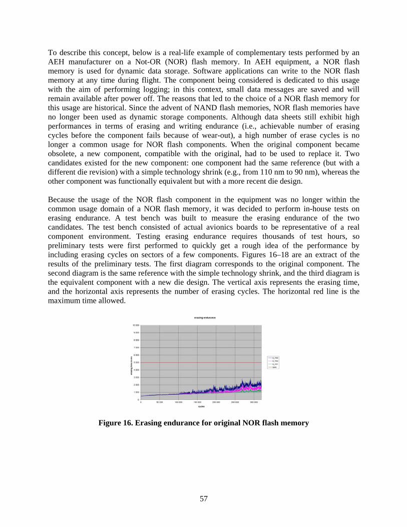
16 Erasing endurance for original NOR flash memory 57
17 Erasing endurance for the same reference with simple technology shrink option 58
18 Erasing endurance for the new die design option 58
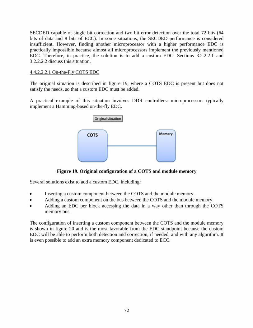
19 Original configuration of a COTS and module memory 72
20 Custom on-the-fly EDC inserted between the COTS and module memory 73
21 Custom on-the-fly EDC inserted on the bus between the COTS and module memory 74
22 Custom per block EDC inserted on the internal bus of the COTS component 75
23 Original configuration of a memory with COTS per block EDC 75
24 Custom per block ECC replacing COTS ECC 76
25 Custom per block ECC added as extra data 76
26 Example of RAID5 principle applied to commodity memory 81
vii
LIST OF TABLES
Table Page
1 List of commodity memories selected for the research 3
2 Summary of available documentation 18
3 Relationship between package constituents and package functions 42
4 Synthesis of die defects 44
5 Synthesis of memory defects induced by packaging 45
6 Summary of mitigation per memory type 47
7 Example of ECC status table 52
8 Main advantages and drawbacks of redundancy options 64
9 Example implementation of redundancy using existing memory components 66
10 Example use of redundancy using existing memory components 66
11 Summary of mitigation techniques versus fault types 83
12 Summary of improved mitigation per memory type 88
13 Template for recommendations 89
viii
LIST OF ABBREVATIONS AND ACRONYMS
AEH Airborne electronic hardware AFE Authority for Expenditure ASIC Application-specific integrated circuit BCH Bose-Chaudhuri-Hocquenghem BGA Ball grid array BTI Bias temperature instability CFR Code of Federal Regulations CMOS Complementary metal-oxide semiconductor COTS Commercial-off-the-shelf CRC Cyclic redundancy code DDR Double data rate DRAM Dynamic random access memory ECC Error correcting code EDC Error detection and correction EEPROM Electrically erasable programmable read only memory EM Electro-migration FMEA Failure modes and effects analysis FPGA Field programmable gate array HCI Hot carrier injection IC Integrated circuit ISO International Organization for Standardization JEDEC Joint Electron Device Engineering Council LER Line-edge roughness MLC Multi-level cell MOS Metal-oxide semiconductor MRAM Magnetoresistive random access memory NAND Not-AND NDA Non-disclosure agreement NOK Not Okay NOR Not-OR NVSRAM Non-volatile static random access memory OK Okay PCB Printed circuit board PLD Programmable logic device PROM Programmable read-only memory QDR Quad data rate RAID Redundant arrays of independent drives RAM Random access memory RDF Random dopant fluctuation RTN Random telegraph noise RTS Random telegraph signal SDRAM Synchronous dynamic random access memory SDS Software and Digital Systems SECDED Single error correction, double error detection SEU Single event upset
ix
SIV Stress-induced voiding SLC Single-level cell SRAM Static random access memory STT Spin transfer torque TCE Thermal coefficient expansion TDDB Time-dependent dielectric breakdown TLC Triple-level cell Vth Threshold voltage WSE Write soft error XOR Exclusive logical OR
x
EXECUTIVE SUMMARY
This report deals with the main issues of using commodity memories in avionics, including safety-critical products. Because of the competitive nature of manufacturers to produce devices that have vast numbers (i.e., millions and possibly billions) of these memories, their quality can be suspect and their reliability and availability are likely to be less robust. This report explains the reason for the concern and investigates methods employed to ensure the reliability of the data stored in commodity memories. Four types of commodity memories are covered in this report to illustrate the nature of the issue. Double data rate memories and Not-AND flash memories are currently being used in avionics products, whereas toggle magnetoresistive memories and quad data rate memories are foreseen to be widely used by aerospace equipment manufacturers in the near future. This report provides a brief description of the technologies, manufacturing aspects, and the state-of-the-art defect management that is used during the manufacture of these technologies. Confidence in commodity memories is built not only from matching their type to the domain usage in the design phase but also by actively engaging with two key entities in the supply chain: the commodity manufacturer and the distributor. This engagement is required to access necessary supporting documentation and understand internal workings not otherwise accessible. A non-disclosure agreement is required, although it might not be sufficient on its own. Failure modes and failure mechanisms for the selected commodity memories are discussed to illustrate the concern. Failure modes in commodity memories are described by using both a black-box and grey-box model view and applying three levels of abstraction: functional, logical, and physical. This organization of information allows for the description of generic functional failure modes associated with writing, preserving, and reading data in a memory; description of failure modes associated with data flows; and refinement of failure mode analysis using physical characteristics. For each of the selected types of commodity memories, this report provides specific examples of functional failure modes applied to each of the data flows. Failures associated with the die and packaging are presented in this report. For each defect type, the impacted memory components, as well as the type of error (soft or hard) and the potential systematic impact at production batch level, are identified. Ensuring the reliability of these commodity memories is investigated through the existing fault mitigation techniques (e.g., Error Correcting Codes [ECCs]) embedded in these memories and the identification of additional internal or external fault mitigation techniques. ECC represent the typical built-in mitigation technique for each of the selected commodity memory types. The mitigation may be implemented by the manufacturer, user, or both. Little or no information is publicly available regarding the embedded ECC for three of the covered types of memory, reinforcing the earlier finding that the airborne electronic hardware (AEH) manufacturer should interact with the memory manufacturer to not only understand the existence of mitigation but the possible configurations and limitations as well. Issues with built-in mitigation techniques typically point to a lack of documentation or poor coverage of the AEH usage domain. Analyzing the effectiveness of the built-in mitigation techniques should be done with respect to the number of errors and type of triggering events the mitigation can handle. The analysis must cover all elements of the embedded mitigation. The approach can be theoretical or experimental, but in both cases sufficient information can be obtained only via the memory manufacturer.
xi
After the use of memory tests to reduce the likelihood of occurrences of data alteration, additional mitigation can be obtained through the use of external means, such as redundancy, or by enhancing the error detection and correction capability of the memory (or a combination of both). For each of the selected commodity memories, the report provides recommendations detailing the applicability of each technique. Finally, the report presents a series of recommendations to support the safety assurance of commodity memories in avionics products. The recommendations are organized by the supply chain selection and control, definition of usage domain, and management of manufacturing defects for each type of selected commodity memory.
1
1. INTRODUCTION
1.1 BACKGROUND
Commercial-off-the-shelf (COTS) items are increasingly penetrating into both the commercial and the military segments of the aerospace market. RTCA standards, namely DO-254 “Design Assurance Guidance for Airborne Electronic Hardware” [1] and DO-178C “Software Considerations in Airborne Systems and Equipment Certification” [2], were developed with the issue of COTS assurance in mind. However, these standards do not recommend specific methods or objective criteria for COTS safety assurance and airworthiness. In a general context of airworthiness, the focus of this report is threefold: • Intended function (Title 14 Code of Federal Regulations Part [14 CFR] 2x.1301):
component selection from a functional standpoint and design to meet the function contributing to this aspect.
• Operating conditions (14 CFR 2x.1309): component selection from the point of view of characteristics and performance and environmental qualification of these components contribute to this aspect.
• Safe operation (14 CFR 2x.1309): failure modes and failure mitigation of the selected components contribute to this aspect. Reliability considerations are integrated into the demonstration of achievement of safe operation.
The research thrust on COTS Airborne Electronic Hardware (AEH) assurance methods addresses “safe operation” and supports the development of a comprehensive framework for COTS safety assurance. The framework includes: • The understanding of current and foreseen future use of COTS in AEH. • The description of safety issues and concerns. • The documentation of failure modes for these COTS and the relevance to AEH context. • The investigation of existing mitigation techniques and their effectiveness. • The development of objective criteria for determining the effectiveness of safety and
airworthiness assurance methods for AEH integrating the COTS under consideration. Previous research under Authority for Expenditure (AFE) project 75 (COTS AEH Assurance Methods) documented 22 COTS issues and proposed a structure to address future COTS AEH assurance standards [3]. A continuation of the research on the identified issues with COTS is currently allocated in part to a supplement to AFE project 75 phase 3 research task order under the Software and Digital Systems (SDS) program, whose focus is commodity memories and embedded microcontrollers [4]. This report is produced under the SDS program. It refines the more general COTS AEH assurance methods for the use of commodity memories. In the process of describing the COTS commodity memories in AEH, considerations of intended function and operating conditions are integrated into the discussion.
2
1.2 PURPOSE
This report deals with the main issues of using commodity memories in avionics, including safety-critical products. Because of the competitive nature of the efforts by manufacturers in producing devices that have vast numbers (i.e., millions and possibly billions) of these memories, their quality can be suspect and their reliability and availability are likely to be less robust. The report explains the reason for the concern and investigates methods to ensure the reliability of the data stored in commodity memories. Several types of commodity memories are covered in this report to fully illustrate the nature of the issue. They are currently being used or might be used in the near future by aerospace equipment manufacturers. For the selected commodity memories, failure modes and failure modeling are being discussed to illustrate the concern. Assuring the reliability of these commodity memories is investigated through the existing fault mitigation techniques (e.g., Error Correcting Codes [ECCs]) embedded in these memories and the identification of additional internal or external fault-mitigation techniques. Finally, the report presents a series of recommendations to support the assurance of commodity memories in avionics products. Disclaimer: In this report, we may state that some COTS components in which the primary target is the consumer electronics market exhibit a level of quality that does not meet AEH quality requirements, especially for safety-critical applications. This statement does not mean in any way that the manufacturers may be lax or incompetent. What is meant is that manufacturing and supply processes that are perfectly rigorous and appropriate for the consumer electronics market may not meet AEH requirements. 2. IDENTIFICATION OF COMMODITY MEMORIES FOR AEH PURPOSES
This section contains introductory material, including descriptions of various types of commodity memories that are being used and might be used in the near future by aerospace equipment manufacturers. The description is set in a context for which the initial market of these memories is not the aerospace market, which has a direct consequence on the type of issues that can be encountered with these products (i.e., because the non-aerospace market controls this initial market, the aerospace industry does not have a great influence on the issues that will be mainly handled by that other industry). 2.1 PROBLEM STATEMENT
By definition, a commodity is a mass-produced, unspecialized product. The main market for commodity memories is consumer electronics, whose characteristics include: • A very large production volume. • A very high level of competition. • Pressure to achieve the shortest possible time to market. • A fast technology refresh cycle (i.e., short time lapse to the next generation). • A short market lifetime of consumer devices embedding memories.
3
As a consequence of the last two bulleted items above, the continuity of support for a given generation of commodity memory is limited. The level of quality of memories, although meeting relevant safety standards and regulations (e.g., ISO-2859-1 [5]), is mainly driven by trading considerations. In consumer electronics, the failure of a memory is likely to impact the end-users’ satisfaction level rather than their safety. This market context is quite different from the avionics market, for which safety is a major driving force. From consumer electronics market characteristics, AEH manufacturers could fear that the intrinsic competitive pressure may eventually result in a slightly lowered quality of the commodity production. This lower quality would still be fully compatible with consumer electronics safety standards, but it may not be adequate for avionics safety requirements. Therefore, the question is not whether commodity memories are of good quality but whether commodity memories have the level of quality adequate for AEH. 2.2 SELECTED TYPES OF COMMODITY MEMORIES
This section describes commodity memories selected for their current widespread use and their foreseen widespread use. The objective of this section is to provide a purposely short and simplified technical description sufficient to promote the understanding of the issues associated with the use of commodity memories in AEH and the subsequent discussion on failure mode and failure mitigation. Table 1 lists the commodity memories selected for this investigation along with their usage level from a market standpoint.
Table 1. List of commodity memories selected for the research
Memory Type Usage Level and Market DDR SDRAM Widely used in consumer electronics market QDR RAM Mainly used in industrial applications NAND FLASH Widely used in consumer electronics market MRAM Not yet widely used but may be in the near future
DDR = double data rate; SDRAM = synchronous dynamic random access memories QDR = quad data rate; NAND = not-AND; MRAM = magnetoresistive random access memory
2.2.1 Double Data Rate Synchronous Dynamic Random Access Memories
Double data rate (DDR) synchronous dynamic random access memory (SDRAM) is present in force in consumer electronics devices. It represents a massive and very competitive market with a high production volume and growth rate. DDR SDRAMs are widely used in AEH as the main memory of almost all processors. They are also often associated with programmable logic devices (PLDs) and application-specific integrated circuits (ASICs) for building large memory areas that would not otherwise fit inside the PLD or ASIC. The wide use of DDR memories stems from their combining large capacity and high performance with relatively low cost. Because DDR memories are a critical type of memory for AEH, they require attention by the aerospace industry.
4
2.2.1.1 Technical Overview
DDR memories are dynamic random access memories (DRAM): the storage element is made of a small capacitor that holds a binary datum (zero or one) corresponding to either a charged or discharged state. This technology enables the memory cells to be smaller than if they were implemented with only transistors. A smaller size allows for higher density, which is the primary reason for the popularity of DRAM. The DDR denomination simply refers to the data bus flow. The data bus transfers one datum on both the rising edge and the falling edge of the clock or two data in a single-clock period. The double rate only pertains to data and only at the external bus interface level. The rest of the die works at the clock rate, including internal data buses. To match the DDR, the internal data bus is simply twice as wide as the external data bus. Successive generations of DDR memories are designated as DDR1, DDR2, DDR3, DDR4, and so on. The difference between the successive generations mainly refers to the operating frequency, as the component architecture and internal operation do not change significantly. The clock frequency is regularly increased to improve data flow performance. The increases primarily affect the interfaces while keeping the increase in intrinsic speed of the memory cell to a minimum. The external growth of the data rate is obtained by simultaneously accessing a greater number of memory cells. For example, consider a memory array working internally at 100 MHz: reading simultaneously 32 internal bits supports 8 bits at 400 MHz on the external bus, while reading simultaneously 64 internal bits supports 8 bits at 800 MHz on the external bus. Raising the clock frequency requires not only improvement on the silicon technology but also on the low-level electrical interface between the memory chip and the board. Examples of such improvements on the electrical interface include lower voltage range, automatic skew compensation, and line-termination management. Changing the electrical interface has non-negligible consequences: successive generations of DDR memories are incompatible. 2.2.1.2 Manufacturing Aspects
As the memory capacity grows, the scale of the transistors and capacitors is reduced, as is the supply voltage. Producing capacitors that have both a small surface on the die and a capacitance that remains high enough to store a significant amount of electrical charge under a lower voltage is rather difficult. Each manufacturer has its own—and generally confidential—method for solving this problem. Sample solutions include implementing capacitors with vertical shafts (the surface of the capacitor being the surface of a cylinder) that take advantage of the third dimension to increase the area of the capacitor while maintaining a small footprint on the die. Furthermore, special materials can cause the surface of the shaft to be granular, which increases the useful area. Finally, internal charge pump mechanisms may be implemented to feed the capacitor with higher voltages than the chip’s supply voltage. Regardless of the realization, the solutions described above increase the risk of producing bad memory cells during the manufacturing process. On the other hand, rejecting a die for the sole reason that a single capacitor is defective would have a severe impact on the production yield. The following technique may be implemented to prevent the rejection of die with only a few defective cells: the memory design can include rows of cells additional to the number of rows
5
necessary to achieve the memory size as pointed out by the data sheet. During manufacturing tests, rows with defective cells are identified, and an internal mechanism reroutes the address of each defective row to a (good) spare row (e.g., by using thermal or laser fuses). This mechanism is kept confidential. Publicly available documents describe this method in general terms, but there is no mention of it in the available documentation from the manufacturers. It is mentioned in this report only as a likely implementation. A “good” DDR die is not necessarily a die without defects; rather, a die may possess defects for which a work around has been developed or for which compensation has been applied. 2.2.1.3 Management of Manufacturing Defects
Naturally occurring manufacturing defects are normally managed during the production process either by employing a workaround or by rejecting the dies that cannot be fixed. However, full testing of all memory cells of the die is more expensive than sampling tests or parametric tests. Therefore, one of the concerns is related to the potential risk that the amount of testing will be reduced to minimize the production testing costs. Even if testing is expensive, delivering components with poor quality certainly has a higher cost; indeed, in consumer electronics devices, a DDR memory is a critical component. A defect in a DDR memory chip generally prevents the equipment from working correctly. Moreover, since almost all systems perform a memory test at startup, a faulty DDR memory chip soldered on an electronic board would quickly be detected by the customer, who in turn would be unsatisfied. Therefore, it is unlikely that manufacturers intentionally deliver defective DDR memory chips to customers, who buy them in the tens of millions. However, defects may exist that are unlikely to be visible in consumer electronics devices but more likely to be visible in an industrial or avionics application. For example, consider the problem of bits flipped by intensive reading of the same row of a DDR memory. In common usage, in which a DDR memory is mainly accessed by software, such particular access sequences do not occur. However, in a specific application, such as a DDR memory connected to an ASIC, the repeated access sequence might occur in special cases. For memories intended to be used in consumer electronics applications, adding a production test dedicated to this issue might not be worthwhile. However, for memories intended to be used in industrial or avionics equipment of assurance level A, a full test is desirable because the correct behavior must be guaranteed for all access sequences. In general, the level of testing must be commensurate with the safety level required for operation of that device (e.g., along the lines of a system development assurance level, as shown in the DO-254 guideline document). The production tests and qualification process of the DDR memory chips are important factors for selecting a DDR memory for AEH. Consideration of the supply chain to support this selection is further discussed in section 2.3. 2.2.2 Not-AND Flash Memories
Not-AND (NAND) flash memories are present in most consumer electronic devices. They represent a highly competitive massive market with a significant volume production and growth rate. NAND flash memory technology evolves very rapidly.
6
NAND flash memories are used in AEH, where mass memory is needed, for example, in cockpit display equipment to store images of maps, in-flight management systems (FMS) to store navigation databases, and integrated modular avionics to store varied large databases for the hosted applications. NAND flash memories are popular because of their advantageously combining significant capacity with high integration and low cost. Because of wear, NAND flash memories require specific management in their use. For this reason, they are generally associated with a dedicated microcontroller that offers two services: • A standard interface to the main processor or PLD/ASIC that uses the mass memory
independent of the evolution of the interface of the NAND flash memory chips themselves. This is particularly useful because NAND flash memory chip interfaces evolve quickly to incorporate more improvements to fit with the continuous increases in size and speed of the components. Examples of such standard interfaces are integrated drive electronics and serial advanced technology attachment interfaces.
• The management of all tasks induced by the wear of the component. The evolutions of the wear management are embedded inside the microcontroller and do not impact the rest of the equipment. This is particularly valuable because NAND flash memory chips evolve quickly and wear management must evolve accordingly.
The microcontroller can be separately purchased from the NAND flash memory chips and assembled on the board. Some manufacturers propose integrated solutions in which the microcontroller and NAND flash memory chips are integrated in a single chip (called a compound chip). One must keep in mind that integrated mass memory devices contain NAND flash memory chips. In this case, it is more difficult to have access to information about the actual embedded NAND flash memory chips, so particular attention must be paid to this point when selecting devices. Microcontrollers are not within the scope of the present document, so, therefore, only the NAND flash memory chips themselves will be addressed. 2.2.2.1 Technical Overview
NAND flash memories are flash programmable read-only memory (PROM). Non-volatile memorization is obtained by trapping electrons in a dedicated area near the gate of a metal-oxide semiconductor (MOS) transistor, which changes its characteristics (general principle). Programming and erasing consist of injecting or extracting electrons to or from the electron trap. Reading consists of driving the transistor and measuring the voltage at its output with an analog comparator. Depending on whether or not there are electrons in the trap, the voltage will be different. Injecting or extracting electrons to or from the electron trap requires voltage greater than the chip’s power supply. To generate these higher voltages, the chip contains charge pump mechanisms. Two main variants of NAND flash memory exist: single-level cell (SLC) and multi-level cell (MLC). The SLC variant works in a hybrid manner: the voltage at the output of the transistor can take only two values driven by the presence, or lack of presence, of electrons in the trap. Thus, a single transistor can store one bit of information. The MLC variant works within a multivaried
7
atmosphere. There may be four different amounts of electrons in the trap: empty, one-third full, two-thirds full, or full. The voltage at the output of the transistor can therefore take four different values, and a single transistor can store two bits of information. Another variant exists that uses eight levels, so that a transistor can store three bits of information. It is often referred to as triple-level cell (TLC). This third variant is less frequently used than the two main variants described above because the TLC has significantly lower erase and write endurance. The advantage of the MLC variant, which makes it very popular, is that it provides twice the capacity for the same die area. The drawback of the MLC is that it requires much stricter control of the amount of electrons in the trap. The main consequence is that the MLC wears faster than the SLC. One of the causes of wear is that during programming of erasing, some electrons get caught near the trap and can no longer be removed. These stuck electrons create a bias on the voltage at the output of the transistor. A lower number of stuck electrons is necessary to create a false voltage on a four-level cell than on a two-level cell, and that critical number will therefore appear earlier for an MLC than for an SLC. Also, for similar reasons, the MLC is more sensitive to manufacturing defects than the SLC. An intermediate variant called “pseudo SLC” is proposed by some manufacturers. A pseudo SLC is a die that has been designed for MLC, so that each cell is able to take on four values but is internally underused: only the values “00” (empty) and “11” (full) are used among the four possible values of “00,” “01,” “10,” and “11.” This strategy allows the manufacturer to offer a chip with the same reliability as an SLC device while still using the same die manufacturing chain used for its MLC, allowing the company to save money. Nevertheless, one could imagine that on a given production line, the dies that are sold as pseudo SLC could be those MLC dies that failed the production test as 2-bit per cell but passed the test as 1-bit per cell. It could be a means for the manufacturer to cut their losses by selling these dies as half capacity-chips rather than rejecting them. This is conjecture, of course, but a safety approach must consider all cases; auditing the manufacturer is a key point. Finally, a new generation of NAND flash memory is emerging as a three-dimensional variant. In this variant, several layers of cells are stacked one on top of the other on the same die. This is different from having several dies stacked one on top of the other. The three-dimensional variant consists of a single die built in a one-shot process. This technology is too recent to have accumulated enough service experience, so it is not taken into account in this report. Two main sources produce defects in a NAND flash memory: manufacturing and wear. Wear occurs during erase, read, and program operations. There are two types of wearing effects: • A temporary effect: some bits will “dim,” possibly up to the loss of their information, but
only the stored information is affected. The memory cell is intact and will work correctly at the next erase or program operation.
• A permanent effect: some internal elements break and can no longer be used. These elements may be individual cells (or sets of cells) or elements common to several cells, such as an erasing mechanism (charge pump for instance).
8
Normally, reading only causes data dimming, which may result in data loss but not in permanent damage. 2.2.2.2 Manufacturing Aspects
NAND flash memories have a very high density and embed a very large number of cells. It is expected that some cells are defective at the end of the die-manufacturing process. Because of the very high volume and very competitive market, it is not desirable to reject a die simply because one or a few cells are defective. Therefore, dies shipped to customers actually contain defective cells. The component contains an internal table at a dedicated location in the memory array, which contains the list of the defective cells so that the users can manage them on their own. The situation in which a new product is expected to contain defects may be seen as beneficial for AEH because the manufacturers must provide facilities to handle these internal defects. Conversely, the percentage of defective chips that may be acceptable for consumer electronics might not be acceptable for AEH. 2.2.2.3 Management of Manufacturing Defects
As previously explained, NAND flash memories have initial defects in addition to the defects that will appear during the component life. All components that manage NAND flash memories will always include mechanisms (hardware or software, or both) to manage these defects. In addition, built-in facility assists in the management of defects: extra bytes dedicated to storing ECC are provided on the memory chip. The management of the ECC (computation, verification, and data correction) must be undertaken by the user. In addition, extra data bytes are provided on the die. Consider the following theoretical example for a 100 MB nominal capacity for which the die may actually host 110 MB of data cells. The user never uses more than 100 MB. During the life of the product, some datasets fail and become unusable. The user stops using the defective cells and begins to use some of the spare cells instead, thus maintaining a usable memory space of 100 MB. The memory chip must be replaced when the amount of working memory cells fall under the minimum required for the system to work correctly. The detection of defective data blocks is made at three distinct times: • Erase time: If the erase operation fails, the chip provides a status informing the user that
the operation failed. The corresponding block should be considered defective. • Program time: If the write operation fails, the chip provides a status informing the user
that the operation failed. The corresponding block should be considered defective. • Read time: When a set of data is read, the ECC must be verified by the user to check the
integrity of the read data. If the ECC reports errors, the user may decide whether to carry on using this data block or declare it defective. The decision is user-defined and may rely for instance on the status of the ECC (e.g., number of altered bits) or on a counter that indicates how many times this block has reported ECC errors despite events, such as erasure or program cycles.
9
It is the responsibility of the user (consumer or AEH user) to maintain a list of the data blocks identified as defective. This list may itself be stored in the NAND flash memory, provided that enough care is taken, typically through redundancy. Management of the remapping of failed blocks versus spare blocks must be made by the user. Placing the above information in the context of AEH requirements, the following should be considered: • The ECC has a limited capacity in terms of number or erroneous bits that can be correctly
detected. If there are too many faulty cells, the ECC will produce a false status. A concern should therefore arise when manufacturing quality unreported by testing leads to defective cells whose number exceeds the ECC capability.
• If the cells wear too quickly, the life duration of the component will be too short with respect to AEH requirement (including an end-of-life event in flight). The defects appearing during the life of the component are not detected by quality control at delivery. A concern should therefore arise when the manufacturing quality process does not, or does, limit wear-endurance testing.
These considerations tie to the selection of a reliable supply chain, as detailed in section 2.3. 2.2.3 Quad Data Rate Memories
Quad data rate (QDR) memories are a special type of static random access memory (SRAM). The QDR memory market is mainly an industrial one focused on the telecommunication domain for ground stations managing traffic routing. These memories seem to have been created specifically to address this purpose. Although the quality level required by telecommunication applications is not that of safety-critical applications, it is higher than that required for the consumer electronics market because a failure of one such ground-heavy station has greater financial impact than a failure of one personal device. From an AEH concerns point of view, QDR memories are less subject to risk than the types of memories previously discussed. Finally, QDR memories are generally not present in consumer electronics devices because of their higher price. Therefore, DDR memories are preferred in the consumer electronics market. QDR memories are used in AEH but not as widely as the other types of memories because their cost is much higher than DDR memories. They are used when very high throughput is required and a relatively low capacity (i.e., a few megabytes) is acceptable. Whenever possible, DDR memories are preferred because they are cheaper. For cases in which DDR memories do not offer the necessary throughput, QDR memories are preferred despite the added cost and lower storage capacity. QDR memories offer two advantages over DDR memories: • A separate data-in and data-out bus, allowing simultaneous read and write operations at
different addresses • A low read latency—typically two clock periods instead of seven or more for the DDR
memory—which allows much better performance for random accesses
10
QDR memories are mostly associated with PLD and ASIC because of their dedicated use and because their specific bus is generally not available on processors and microcontrollers. A typical application is network switch engines, for which frame management requires a high data exchange with buffer and configuration memories. Simultaneous read and write is an advantage because as much data need to be written to the buffers as to be read from them. Also, configuration memories (like routing tables) require random accesses and the low latency of the QDR memories is beneficial. 2.2.3.1 Technical Overview
The storage cell of a QDR memory is made only with complementary metal-oxide semiconductor (CMOS) transistors. Contrary to the other types of memories discussed in this report, there is no specific technology associated with QDR memories. What distinguishes them from other SRAM is their bus interface. The bus interface is comprised of two separate and independent data buses: a data-in port for write operation, and a data-out port for read operations. The buses can operate simultaneously. Each data port works at DDR on the same model as the DDR memory: data are transferred on both the rising edge and the falling edge of the clock, thus transferring two data words per clock period. Data are generally transferred by bursts of four data words, which then take two clock periods. The address and control bus is common to read and write, but address and control need to be stable for only one clock period—either for read or for write. Therefore, during two clock periods, the QDR memory is capable of: • Receiving a read address and receiving a write address (one clock period each). • Receiving four data words for write (two data words per clock period). • Providing four data words for read (two data words per clock period). These tasks are possible only if the adequate pipelining is employed. Moreover, being an SRAM, QDR memories have no notion of bank, row, column, or refresh like DDR memories. Only the address is necessary to make a read or write operation and the address bus is not multiplexed; rather, it carries the full address. It is possible to have a continuous data flow of two data words per clock period on both the read port and the write port, even if the addresses are random (i.e., not contiguous). 2.2.3.2 Manufacturing Aspect
The QDR memories use only CMOS transistors, like any SRAM. There is no specific manufacturing aspect. 2.2.3.3 Management of Manufacturing Defects
The QDR memories’ target is the industrial market, with the management of manufacturing defects expected to be rigorous.
11
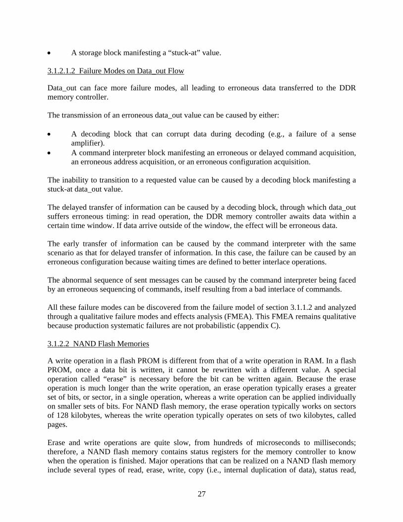
2.2.4 Toggle Magnetoresistive Random Access Memories
Magnetoresistive random access memory (MRAM) is a special type of random access memory (RAM). It has the same characteristics as a RAM (random accesses, fast read and write accesses, no wear in use), but it is also non-volatile (the content is fully preserved when the power supply is cut off). The MRAM combines the advantages of RAM and PROM. The qualifier of “toggle” refers to the method used internally to manage memory cells. Toggle MRAMs are medium-range capacity memories, typically two megabytes per chip. Very few manufacturers produce toggle MRAM and some of them do so only for their internal usage, without selling them on the market. A significant part of the toggle MRAM market is dedicated to industrial applications, with toggle MRAM rarely found in consumer electronics. For AEH, only one manufacturer produces these memories. This is EVERSPIN, which recently granted licensing rights to one company. Toggle bit MRAM are used in AEH as non-volatile memory when both of the following conditions exist: a medium storage size is needed (typically a few megabytes) and fast random read and write operations are required. For large amounts of non-volatile data (hundreds of megabytes to gigabytes), toggle bit MRAM is not suitable because of the limited size of the chips. In this case, flash PROM is needed. However, when fast random read and write operations are required, flash PROM is not suitable because of its slow access time, especially for write operation, which additionally requires an erase operation. Toggle bit MRAM can replace the more classical technologies: • Electrically-erasable programmable read only memory (EEPROM): the parallel
EEPROM market is decreasing. Therefore, EEPROM is not considered a good solution for future designs.
• Non-volatile static random access memory (NVSRAM): NVSRAM is a combination component that contains an SRAM and a PROM on the same die. The user works only with the SRAM, thus enjoying the performance of an SRAM. At power up, the component automatically copies the contents of the PROM into the SRAM. At power down, the component automatically copies the contents of the SRAM into the PROM, thus providing the appearance of an SRAM that keeps its contents across power cycles.
From the functional standpoint, NVSRAM and MRAM are similar. From the standpoint, NVSRAM combines two established technologies (SRAM and PROM), whereas MRAM uses a new technology (magnetic cells). 2.2.4.1 Technical Overview
Toggle MRAM uses the physical property of two materials: • A ferromagnetic material whose magnetic polarization can be changed electrically: once
the polarization has been electrically set to a value, the material keeps it until another electrical action changes it. This denotes the toggle element. The change in magnetic
12
polarization allows for writing the information into the memory cell. The toggle property of the material provides data retention even after power off.
• A second material whose electrical resistance changes depending on the magnetic field which passes through it. The second element is placed near the first one to be under the influence of its magnetic field. Measuring the electrical resistance of the second element allows for the information of the memory cell to be read.
This system has several advantages: • Read and write operations are as fast and flexible as with RAM. • Data retention (unpowered) is as good as with PROM. • There is no wear out. The main limitation of the toggle MRAM comes from the method used to electrically change the magnetic polarization of the storage element. An electric current first generates its own magnetic field. This magnetic field, in turn, influences the toggle element and, depending on the electric current direction, changes the toggle element into one state or the other. If two memory cells are too close to each other, the magnetic field generated to toggle the first one may cause the second to toggle, because of proximity, as well. Therefore, the integration factor of toggle MRAM is limited: it is not possible to set the cells too close to one another. Because this limitation comes from physics of the method used to force the toggling, and not from the foundry, toggle MRAM using this method will not see a significant growth in size in the future. Other methods are under development for toggling that do not exhibit this drawback and therefore will allow higher integration (section 2.2.4.4). Despite the limited integration scale, writing into a cell may still influence a nearby cell, and, in rare cases, cause it to toggle, thus creating a soft error. For this reason, a toggle MRAM chip includes embedded ECC that allows for providing good data at the pins of the chip on read, even when an internal bit is altered. 2.2.4.2 Manufacturing Aspect
Although MRAM involves special materials, the fabrication process flow is the same as for standard CMOS RAM. It is even possible to embed toggle MRAM cells in an ASIC. The intrinsic limitation of the toggle MRAM integration may have an unexpected advantage from the point of view of manufacturing defects: as toggle MRAM cannot be scaled down, submicron foundries are not worth using. MRAM uses more conservative technologies, which can reduce the manufacturing efforts and risks. Moreover, the medium-capacity range (16 megabits)—when compared to the DDR memories or flash memories (gigabits)—advocates in favor of risk reduction. 2.2.4.3 Management of Manufacturing Defects
No public information is available about managing manufacturing defects (redundancy, remapping, or other). Components are delivered fully functional and with full capacity.
13
Embedded ECC seems to aim at mitigating write soft errors (WSEs) but not permanent manufacturing errors. 2.2.4.4 Spin Transfer Torque Magneto-Resistive Random Access Memory
Spin transfer torque (STT) MRAM belongs to the MRAM family. The difference between toggle MRAM and STT MRAM resides in the method used to change the magnetic polarization of the ferromagnetic element (section 2.2.4.1). The SST MRAM uses a quantum effect instead of an explicit magnetic field. This reduces the crossover between cells during writing and, therefore, allows for a much greater integration. SST MRAM technology is seen as possessing high potential for both non-volatile and simple memory, with capacity in the gigabits. The SST MRAM technology is still under development; prototypes exist, but to date there is no mass production. Were STT MRAM to achieve a density level greater than DDR memory, and with equivalent performance, it would likely take the lead in the memory market. Although there is not enough information available to include this technology in the scope of this report, it should be on the watch list for the coming years. 2.3 SUPPLY CHAIN CONSIDERATIONS
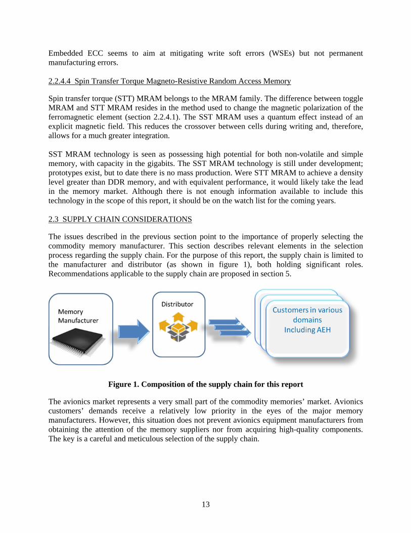
The issues described in the previous section point to the importance of properly selecting the commodity memory manufacturer. This section describes relevant elements in the selection process regarding the supply chain. For the purpose of this report, the supply chain is limited to the manufacturer and distributor (as shown in figure 1), both holding significant roles. Recommendations applicable to the supply chain are proposed in section 5.
Figure 1. Composition of the supply chain for this report
The avionics market represents a very small part of the commodity memories’ market. Avionics customers’ demands receive a relatively low priority in the eyes of the major memory manufacturers. However, this situation does not prevent avionics equipment manufacturers from obtaining the attention of the memory suppliers nor from acquiring high-quality components. The key is a careful and meticulous selection of the supply chain.
14
2.3.1 Memory Manufacturers
This section focuses on specific characteristics relevant to the components’ supply for avionics applications. Several criteria distinguish the memory manufacturers: targeted market, rate of product upgrade, and available documentation. 2.3.1.1 Targeted Market
The first criterion pertains to the market that is targeted by the manufacturer. Three main cases can be distinguished: 1. Case 1: Manufacturers that have a business model exclusively geared toward consumer
electronics This kind of manufacturer should be avoided or is at least not highly recommended because its mission statement does not entail avionics requirements; as a result, there could be confidence issues associated, for example, with reliability or environmental qualifications. If a given memory component was provided solely by this type of memory manufacturer, this component should be replaced by another one in the design. However, if such a component is necessary, a possible workaround would be to perform complementary tests, such as burning or screening, on the component to increase the level of confidence in the component. These tests can be performed internally or in collaboration with a third party specialized company. 2. Case 2: Manufacturers with a business model that is primarily geared toward consumer
electronics but who also have an industrial range of products This case is more favorable than case 1. The components in the industrial range will be manufactured employing industrial quality standards. The risk of harmful effects from the consumer electronics market is lower. The most favorable case is when the manufacturer has an automotive range of products because the automotive market is a relatively high-volume market with a relatively high-quality set of requirements. This case also includes a safety domain, including rail, nuclear, and medical. 3. Case 3: Manufacturers that have a business model primarily geared toward a specialty
market that demands high integrity and continued support This is the best case because these manufacturers are not, or at least they are significantly less likely to be, subjected to the pressure of the consumer electronics market to compromise quality. 2.3.1.2 Rate of Product Upgrade
The second criterion pertains to the upgrade rate of the components. Component modifications, such as die revision (improvement), technology shrink, or component versioning (e.g., memory size or speed), can occur. Sometimes, the manufacturer’s strategy is to continuously offer the latest technology with the best available performance. This strategy often leads to negative results, such as short sale duration of products, rapid obsolescence, and a fast process shrinking
15
rate. The risk induced by this strategy is that the manufacturer might feel it is not worth investing more effort than necessary to increase the production reliability for such a short life cycle. Another drawback of this strategy, from an AEH point of view, is that the new technology has no service experience and may have intrinsic defects or weaknesses that are not yet known. Moreover, the strategy of being first to market may lead the manufacturers to create temporary revisions of the chips they sell, a fact about which the buyer is seldom properly informed regarding the chips’ temporary nature. As an example, consider manufacturers who sold an intermediate version of their chip by buying equivalent dies from another foundry (a competitor) and repackaged these dies into their own packages with their own references. This approach allows the manufacturer to be present on the market while its foundry ramps up the capability to produce its own dies. From a technical and commercial point of view, there is absolutely nothing wrong with the approach because the dies meet both quality and performance level. However, from the point of view of avionics requirements, for which traceability is a concern, this situation is undesirable. AEH manufacturers should therefore avoid such memory manufacturers. However, this is not always possible because the avionics market has its own goal to keep providing more performance at lower costs. Also, the interest of an avionics manufacturer may primarily stem from obsolescence issues. Well-proven technologies may sometimes be too limited to satisfy the performance requested by a given product. In this situation, particular attention shall be paid to the components, as detailed in section 2.3.1.3. Assiduous contact with the memory manufacturer can help AEH manufacturers to avoid the purchase of new memories that are being manufactured by second-hand manufacturers. However, other manufacturers rely on well-proven technologies and propose mature components with longer term production cycles. These manufacturers often take over components that were initially provided by the first type of manufacturer. When the first type of manufacturer ceases production (obsolescence), the second type commences manufacturing; as much as possible, this latter type of manufacturer should be preferred. 2.3.1.3 Available Documentation About the Manufacturing Process
A third criterion relates to the availability and extent of documentation. Some memory manufacturers provide documentation on their manufacturing flow, test flow, and qualification processes and results, whereas others do not. The more extensive the documentation, the higher the level of confidence in the product. This kind of documentation is generally not public since it contains intellectual property, but it may be available under a non-disclosure agreement (NDA). When selecting a manufacturer, the accessibility to manufacturing documentation is an important consideration. There are several major topics addressed by manufacturer documents: design, technology, manufacturing tests procedures, manufacturing tests results (statistics), qualification processes (including a description of the qualification tests), qualification reports (including the detailed test results), errata sheets, and white papers on continuity of support for obsolescence management.
16
2.3.1.3.1 Information About the Design
Useful examples of this information include: • Information about the physical proximity of the memory cells on the die with respect to
their logical proximity in the address space and data words. • Information about special internal functions, such as charge pumps, that does not appear
in the data sheet. This information is confidential but may be obtained, at least partially, under an NDA. This information is generally very useful for analyzing risks and mitigation mechanisms. However, special care should be taken because some aspects of the design can change noticeably from one revision of the die to another. For example, memory can be produced in which the relative position of the cells on the die, versus their position in the data words, was significantly different in the successive revisions of the die. It was not a real design change, only a different type of routing—but for ECC consideration, it was an impacting change. Therefore, the relevance level of the design information must always be moderated by its validity in time. Some design elements may be key points for the memory manufacturer and will, therefore, remain stable across the successive revisions of the memory. For example, the memory manufacturer may have made the commitment to implement a built-in ECC mechanism with a tricky association between the physical cells and the logical bits of the ECC algorithm, so that the ECC is as efficient as possible with respect to the possible soft errors. In this case, if the layout of the cells changes from a die revision to another, the design of the ECC will change accordingly, and the ECC performance will remain unchanged. To summarize, the information about the design is extremely useful, but it must not be taken as a standalone piece of information. A discussion with the memory manufacturer is absolutely necessary to get the status of each important design choice of a given product and learn whether it is a long-term choice or simply a contextual one. 2.3.1.3.2 Information About the Technology
This information is highly confidential and generally not available to the AEH manufacturer. In general, the scheme is as follows: • The AEH manufacturer can enter into an NDA with the component manufacturer. • The component manufacturer has an NDA with the foundry. However, the scheme is not transitive: the component manufacturer cannot transmit the design information, the property of the foundry, to the AEH manufacturer. The foundry will not grant an NDA to the AEH manufacturer because the latter is not one of its direct customers. Even when the component manufacturer runs its own private foundry, the information is often considered as too sensitive and rarely provided.
17
2.3.1.3.3 Information About Manufacturing Test Procedures
Although this information is essential for addressing most of the concerns within the scope of this report, detailed information is generally not available: first, it is considered highly confidential and, second, it pertains not only to the memory manufacturer but also to the foundry. There may be an advantage, as sometimes general information can be obtained. As a general rule, however, one cannot rely on the availability of this information. 2.3.1.3.4 Information About Manufacturing Test Results
Test results are mainly statistics on measured parameters and ratios of accepted, versus rejected, dies. By themselves, they may be very interesting with respect to the objectives of this report. However, once again, this information is rarely available because it is considered highly confidential and pertains not only to the memory manufacturer but also to the foundry. Finally, information about production yield ties to financial information and, therefore, is not disclosed. 2.3.1.3.5 Information About the Qualification Process and Associated Report
This information does not concern the whole production set but rather the characteristics of the component itself, measured by way of a limited number of components (generally several hundred). Qualification tests are different from production tests: • The aim of production tests is to check that the components are manufactured correctly.
The result is binary (indicating either okay or not okay). • The aim of qualification tests is to check that the design and production chain provide
chips that have the expected performance. The results have probabilistic values. The detailed qualification process and associated results contain a significant amount of useful information about the inside of the component, including elements of design that are not necessarily published in the data sheet. It may also indirectly provide information detailing on which parameters of the component the manufacturer focuses. Knowledge of the qualification process and the associated results surely support achieving higher confidence in the components. It is generally possible to obtain these documents (detailed process and report) under an NDA. To summarize, information on the detailed qualification process and associated results is a “must have” and should be obtained from the manufacturer. 2.3.1.3.6 Errata Sheets
Errata sheets are important documents. This is true not only because they are necessary for the board design, but also because they may provide a feeling for the maturity of the component. One of the questions of relevance within the scope of this report is whether time-to-market constraints can cause a component or design to not achieve sufficient maturity. This information can be inferred from the errata sheets. Most of the time, errata sheets are public documents, but sometimes they can only be obtained under an NDA. The component manufacturer should be asked about these.
18
2.3.1.3.7 Summary of Manufacturing Process Documentation
Table 2 summarizes the availability of documentation from the commodity memory manufacturer and its usefulness with respect to confidence in the maturity of the product.
Table 2. Summary of available documentation
Documentation Focus General Availability Usefulness Design Partially under NDA Medium Technology No (IP* protected) — Manufacturing tests procedures No (IP protected) — Manufacturing tests results (statistics) No (IP protected) — Qualification process, including a description of the qualification tests Yes, under NDA High
Qualification report, including the detailed test results Yes, under NDA High Errata sheets (not publicly available) Yes, under NDA Low**
* Intellectual property
** The quality of the information in the errata sheets varies widely. Sometimes, it is not directly usable. The usefulness is thus marked low, although it is possible to find usable errata sheets—for example, to infer maturity based on the rate of errata publication. 2.3.2 Distributors
The fourth and last criterion relates to the role of the distributor. The distributor is a key agent in the supply chain, especially for components like commodity memories that are produced in very high volume―far greater than the volume of the avionics market. They are the link between the memory manufacturer and AEH manufacturer. As previously explained, an AEH manufacturer is generally not in a position to influence a memory manufacturer, but it may be the case for the distributor. Since the distributor concentrates the orders from its own multiple customers, not only from the avionics domain, the distributor is (through aggregated volume) a meaningful customer from the memory manufacturer point of view. This is the first reason to carefully select a distributor. On the other hand, the AEH manufacturer does not only buy memory from a given distributor, but may also buy a lot of other types of components. Moreover, the AEH manufacturer may be part of a bigger company, with activities other than AEH, which brings many components to the distributor. The AEH manufacturer is then a significant customer from the distributor point of view. This is the second reason to carefully select a distributor. Another key role of the distributor is to manage allocation. Memory manufacturers who produce high volumes of components adapt their production to the demand. The production is therefore divided into parts that are allocated in advance to the various customers. The role of the distributor is to obtain a part of the production for each of its customers. This is the third reason to carefully select a distributor.
19
When the demand exceeds, or simply reaches, production capacity, the best customers of the memory manufacturer may be served in priority order. The distributors, because of their sheer size, can secure a part of the production. Finally, the distributor may help the AEH manufacturer to obtain information from the memory manufacturer. This is the fourth reason to carefully select a distributor. The selection of a good distributor is almost as important as the selection of a good manufacturer. 2.3.3 Summary
The selection of an appropriate memory supply chain (i.e., a memory manufacturer and a distributor) is one of the key factors in controlling the level of quality of commodity memory. The present document provides technical information about various techniques that allow for managing issues stemming from the fact that commodity memory manufacturers primarily cater to the needs of consumer electronics. However, before managing the issues with technical solutions, the first step is to reduce the issues with the help of an appropriate supply chain. 2.4 USAGE DOMAIN
Another focal point of COTS usage in avionics is the component’s usage domain in the avionics equipment. Some components have several modes or options that can be selected via the design of the equipment (hardware or software configurations). A defect that is specific to a particular mode or configuration will quickly reveal itself if that mode or configuration is widely used. This defect will then be reported to the manufacturer who, in turn, will either fix the defect or at least document it in an errata sheet. Conversely, if the mode or configuration is rarely used, the defect may remain undetected and therefore not documented anywhere—and may ultimately cause unexpected erroneous behavior. Memory in general has limited possible modes and configurations, but nonetheless these are sufficient for a defect to arise. Such examples include the auto-precharge mode of the DDR memory or the erase suspend mode of a NAND flash memory. DDR memories and NAND flash memories must implement the full Joint Electron Device Engineering Council (JEDEC) specification [6], but it is possible that a particular mode or configuration specified by the JEDEC is not commonly used by the majority of the users of that memory. Memory manufacturers are generally well-informed about the most common usage of their component. The AEH manufacturer should therefore establish a solid line of communication with the memory manufacturer. The distributor also has a role to play in this communication. Moreover, it is recommended that AEH manufacturers employ the most commonly used modes and configurations to the maximum extent possible. The usage of the component in a consumer electronics context is beneficial. As the component is increasingly used by a significant number of users, the probability of detection of possible defects increases. Another facet of usage domain is the selection of one of the possible variants of a memory component. Associated to the same root part number, a component may have several variants, including: • Different speed grade.
20
• Different capacity (e.g., 512 Mb, 1 Gb, and 2 Gb). • Different data bus (e.g., with 8- or 16-bit). For the reason of common usage, the variant in which the production volume is significantly smaller than the other variant should, whenever possible, not be selected. Figure 2 shows a case of a favorable usage domain and one of a less favorable usage domain.
Example of not very favorable usage Preferable usage when possible
Figure 2. Comparison of favorable and not-favorable usage domains
On the left-hand side, the AEH manufacturer usage domain falls in the minor usage category. The memory manufacturer may have spent a lower effort on the qualification tests for that usage because of the small volume of users. On the right hand side, the AEH manufacturer domain usage falls into the main domain usage. Qualification tests and in-use validation levels are higher. The selection of memories for which the AEH manufacturer domain usage falls within the main domain usage (i.e., in terms of users and focus of the qualification tests) is recommended. 3. FAILURE MODES AND FAILURE MECHANISMS
3.1 DESCRIPTION OF FAILURE MODE TYPES IN COMMODITY MEMORIES
This section discusses failure modes for the commodity memories selected in section 2.2. 3.1.1 Issues With Commodity Memories Failure Mode Analysis
COTS memories in general, and commodity memories in particular, should be studied at different breakdown levels [7]—namely, first as a black box and then, when necessary, as a grey box: • As a black box, the memory is considered from the point of view of its inputs, outputs,
and transfer characteristics without any knowledge of its internal workings. • As a grey box, the description of the memory is refined down to internal blocks or
intellectual property, which is then treated as a black box. This breakdown level is built
21
with fragmentary, non-contractual information, and potentially with information disclosed under an NDA.
Note that the breakdown level called “white box” is generally considered inaccessible and useless for the understanding of failure phenomena: at this level, the amount of information is significant, and it can be very difficult to retrieve the useful elements. For example, the characteristics of a memory functional block are not easily extractible from a list of transistors and their characteristics. Nonetheless, when considering the production systematic failures, some manufacturer information at that level (down to the transistor) can be useful. This will be further addressed in the fault model and fault mitigation techniques discussion in sections 3 and 4. In turn, the breakdown levels can be considered at levels representing various abstraction layers. We identified three of these layers as relevant for the investigation of commodity memory assurance methods: the functional, logical, and physical layers [7, 8]. Figure 3 shows this model. Each layer can be accessed directly, depending on the level of abstraction requested by the description model. The vertical arrows in figure 3 represent the conversions between abstraction layers and not data flow.
Figure 3. Three-layer model of a memory
3.1.1.1 Failure Modes at Functional Abstraction Layer
Although no applicative function can be defined for a stand-alone memory, the memory provides hardware functions, such as information storage (writing), information preservation, and information restitution (reading). The generic failure modes at the functional abstraction level are: • The hardware function’s inability to trigger (e.g., no information can be stored).
22
• The hardware function’s inability to stop (e.g., the reading tasks never end and the memory remains unavailable for other tasks).
• The hardware function’s untimely triggering (e.g., a memory untimely triggers a read mode that stops a write command).
• The hardware function’s untimely stopping (e.g., the abort of a write command). • The hardware function’s erroneous behavior (e.g., the modification of data written or
read).
Applying the failure modes listed above to the functions provided by the memory yields: • For information storage (writing):
- The inability to store information - The inability to stop an information storage mode, which leads to memory being
unavailable (e.g., memory is busy in write mode) - The untimely stopping of the information storage function (e.g., storage aborts) - The erroneous behavior of the information storage function (e.g., stored
information is corrupted)
• For information preservation:
- The inability to trigger the information preservation function (e.g., preservation never starts)
- The untimely stopping of the information preservation function (e.g., preservation stops after some delay)
- The erroneous behavior of the information preservation function (e.g., information is corrupted during information preservation)
These three functional failure modes can be summarized as “inability to preserve information.”
• For information reading:
- The inability to read the information - The inability to stop the information read mode, which prevents memory storage
(e.g., memory is busy in read mode) - The untimely stopping of the read function (e.g., read abort) - The erroneous behavior of the information read function
3.1.1.2 Logical Abstraction Layer
This level considers the flow of information that transits on component interfaces at a logical level. A typical flow is data_out. The flow states are precisely defined and consequently a complete failure model can be derived.
23
A failure of a write operation has no immediate visible effect; however, the effects will be visible later, through a read operation, for example. In this case, the write operation is an input flow with no output flow that can bear several failure modes. One way to overcome this property of memories and attribute a failure mode to a write operation is to establish that every write operation in a logical layer has an output in a functional layer; this output is described in the form of an information_stored flow. This stored information can be checked during testing and truly corresponds to an output when the stored information is abstractly assimilated as an output of memory. In this framework, figure 4 (adapted from [7, 8]) shows the several possible behaviors that a transmitted message can exhibit when it is sent to or from a memory and carries informational content.
Figure 4. Tree of possible failure modes
The three groups of behaviors shown in figure 4 are: 1. Correct message sending 2. Failure mode of message sending itself 3. Failure of message sending relative to the other messages These groups are generic and should be tailored to the different messages related to memory output: information stored through write operation, data_out through read operation, and status reading through status request (whose applicability depends on the type of memory).
24
Case 1. The message sent can be correctly delivered to memory. In this case, the information it contains can either: • Case 1.1. Be correct (e.g., the information is correctly written in memory, data_out is
correctly read from memory) or • Case 1.2. Be corrupted in three different ways:
- Case 1.2.1. The information transitions to a forbidden value. Forbidden values occur when logically admissible values are separated from all reachable values by some additive criteria. In memory, this type of corruption does not happen as a memory-stored bit of information, but it can appear in a serial link, like Ethernet, where 8-bit to 10-bit encoding is applied. Some failures of this encoding may then produce forbidden 10-bit values, and the encoded message cannot be interpreted by the receiver. This condition will not be considered hereafter.
- Case 1.2.2. The information transitions to an erroneous value. Contrary to the
transition to a forbidden value, the transition to an erroneous value provides admissible information at the memory’s functional layer. The information will be delivered through read request to the memory controller. This transition does not presume the existence of a higher level mitigation (e.g., external ECC, consistency check at the applicative layer level) that could detect the erroneous behavior of the memory. For a write operation, the information stored is transitioned to an erroneous value; for a read operation, an erroneous data_out value is transmitted.
- Case 1.2.3. The information cannot transition to the requested value. For a write
operation, the information already stored in memory cannot be replaced by a new value. The information remains stuck in some state. For a read operation, data_out may remain stuck at a value in the output level of the memory (output levels of a memory generally contain an SRAM buffer permitting data preparation and fast transfer).
Case 2. The message can be incorrectly sent by itself: • Case 2.1. Lost message is in general not applicable to memory because output flows can
always be interpreted as bits of information. Therefore, the transition failure mode will be considered instead.
• Case 2.2.1. Delayed transfer of message is a degraded mode occurring when the operation takes more time than specified. It could occur if the remapping of addresses on spare cells is not compliant with the datasheet. In the case of a write operation, it can lead to a memory that is unable to receive another order for some time because it is kept busy by the write operation. In the case of a read operation, this failure mode results in a delay in the transmission of data_out.
• Case 2.2.2. Early transfer of message is another type of degraded mode that is more remote and whose effect can be severe in some cases. If a memory has response times
25
significantly different from its specification, the memory controller may not be able to accept the read message and this message can be lost.
• Repeated up to babbling. This mode does not really apply to memory because memory is not a passive component. It does not send messages per se; rather, it presents data on its output bus. But it is the memory controller that decides to pick up the data when it wants. Even if the memory presents a lot of extra data, it will have no effect because the controller will not capture them.
Case 3. The message can be incorrectly sent with respect to other messages, which typically leads to an abnormal sequence of sent messages (case 3.1). This mode can affect data_out. 3.1.1.3 Physical Abstraction Layer
This level includes such physical characteristics as voltage, current levels, timing, and sizing. This abstraction layer can be used to refine the failure modes at logical levels and point to some errors in white box approaches. 3.1.2 Detailed Analysis of the Selected Memory Families
3.1.2.1 DDR Memories
Four major types of operations are performed on DDR memories (figure 5): • Write operation with two variants: with pre-charge (called write_autoprecharge) and
without pre-charge (write). Both types of the write operation send data and an address. They result in an “information stored” state in the functional layer.
• Read operation with the same types of variants as for the write operation. Both types of a read operation send an address, which results in “data_out” emitted.
• Refresh operation with two variants: initiated or self-refresh. • Load_register that allows for configuring some key parameters in the DDR memory, in
particular timings. At a black box level, only two flows are relevant: information stored and data_out emitted. The logical layer failure modes previously described are applicable to each of these flows. To explore the causes of these failure modes, an abstract block diagram of a typical DDR memory is useful, as shown in figure 5.
26
Figure 5. Simplified DDR memory block diagram
3.1.2.1.1 Failure Modes on “Information Stored” Flow
Per the logical failure model described in section 3.1.1.2, the only failure modes that can occur on information stored are transition of information to an erroneous value (case 1.2.2) and inability to transition to requested value (case 1.2.3). Both will result in erroneous data being stored and, ultimately, in erroneous data being transferred to the DDR memory controller through data_out flow: The transition of information to an erroneous value can be caused by: • A command interpreter block manifesting an erroneous command (e.g., a read command
becoming a write command), a delayed command (e.g., misfit of internal pipeline length due to intrinsic obstruction of pipeline), or an erroneously stored configuration (e.g., misfit of internal pipeline length due to corruption of configuration register).
• A coding block manifesting erroneous data (e.g., due to erroneous timing of coding) or an erroneous address.
• A storage block manifesting a loss of refresh (e.g., because of a non-application of initiated refresh command), flip value in time (e.g., because of internal perturbation or external perturbation, current leakage), or flip value on access (e.g., due to failure of the automatic rewrite after a destructive read).
The inability to transition to a requested value can be caused by either: • A command interpreter block manifesting an erroneous command (e.g., misfit of internal
pipeline length due to corruption of configuration register).
27
• A storage block manifesting a “stuck-at” value. 3.1.2.1.2 Failure Modes on Data_out Flow
Data_out can face more failure modes, all leading to erroneous data transferred to the DDR memory controller. The transmission of an erroneous data_out value can be caused by either: • A decoding block that can corrupt data during decoding (e.g., a failure of a sense
amplifier). • A command interpreter block manifesting an erroneous or delayed command acquisition,
an erroneous address acquisition, or an erroneous configuration acquisition.
The inability to transition to a requested value can be caused by a decoding block manifesting a stuck-at data_out value. The delayed transfer of information can be caused by a decoding block, through which data_out suffers erroneous timing: in read operation, the DDR memory controller awaits data within a certain time window. If data arrive outside of the window, the effect will be erroneous data. The early transfer of information can be caused by the command interpreter with the same scenario as that for delayed transfer of information. In this case, the failure can be caused by an erroneous configuration because waiting times are defined to better interlace operations. The abnormal sequence of sent messages can be caused by the command interpreter being faced by an erroneous sequencing of commands, itself resulting from a bad interlace of commands. All these failure modes can be discovered from the failure model of section 3.1.1.2 and analyzed through a qualitative failure modes and effects analysis (FMEA). This FMEA remains qualitative because production systematic failures are not probabilistic (appendix C). 3.1.2.2 NAND Flash Memories
A write operation in a flash PROM is different from that of a write operation in RAM. In a flash PROM, once a data bit is written, it cannot be rewritten with a different value. A special operation called “erase” is necessary before the bit can be written again. Because the erase operation is much longer than the write operation, an erase operation typically erases a greater set of bits, or sector, in a single operation, whereas a write operation can be applied individually on smaller sets of bits. For NAND flash memory, the erase operation typically works on sectors of 128 kilobytes, whereas the write operation typically operates on sets of two kilobytes, called pages. Erase and write operations are quite slow, from hundreds of microseconds to milliseconds; therefore, a NAND flash memory contains status registers for the memory controller to know when the operation is finished. Major operations that can be realized on a NAND flash memory include several types of read, erase, write, copy (i.e., internal duplication of data), status read,
28
and some controls (e.g., reset operation). Figure 6 shows the simplified block diagram of a NAND flash memory.
3.1.2.2.1 Failure Modes on “Information Stored” Flow
Per the logical failure model described in section 3.1.1.2, the only modes that can occur on information stored are transition of information to an erroneous value (case 1.2.2) and inability to transition to a requested value (case 1.2.3). Both will result in erroneous data being stored and, ultimately, in erroneous data being transferred to the NAND flash memory controller through data_out flow. The transition of information to an erroneous value can be caused by: • A command interpreter block manifesting an erroneous command (e.g., a read command
becoming a write command) or a delayed command (e.g., misfit of internal pipeline length due to intrinsic obstruction of pipeline).
• A coding block manifesting erroneous data (e.g., due to erroneous timing of coding) or erroneous address.
• A storage block manifesting a flip value in time due to internal perturbation (e.g., component wear out).
29
The inability to transition to a requested value can be caused by: • A command interpreter block manifesting an erroneous command (e.g., misfit of internal
pipeline length). • A storage block manifesting a “stuck-at” value. • A failure of the erase operation, which will later prevent the write operation from
succeeding. 3.1.2.2.2 Failure Modes on Data_out Flow
Data_out flow can face more failure modes, all leading to erroneous data transferred to the NAND flash memory controller. The transmission of an erroneous data_out value can be caused by: • A decoding block that can corrupt data during decoding (e.g., a failure of a sense
amplifier). • A command interpreter block manifesting an erroneous or delayed command acquisition
or erroneous address acquisition. The inability to transition to a requested value can be caused by a decoding block manifesting a stuck-at data_out value.
The delayed transfer of information can be caused by a decoding block, through which data_out suffers erroneous timing: in read operation, the NAND flash memory controller awaits data within a certain time window. If data arrive outside of the window, the effect will be erroneous data. The early transfer of information can be caused by the command interpreter by way of the same scenario as that for delayed transfer of information. The abnormal sequence of sent messages can be caused by the command interpreter being faced by an erroneous sequencing of commands, itself resulting from a bad interlace of commands (as with early transfer of information). 3.1.2.2.3 Failure Modes on Status
The transition of information to an erroneous value can be caused by a command interpreter block manifesting an erroneous, or delayed, command acquisition. The inability to transition to a requested value can be caused by the status logic when a status register manifests a stuck-at value.
30
3.1.2.3 QDR Memories
Compared to DDR memories and NAND flash memories, QDR memories are very simple to operate. Only two operations can be realized (write and read) that result in “information stored” and “data_out,” as shown in figure 7.
Figure 7. Simplified QDR memory block diagram
3.1.2.3.1 Failure Modes on “Information Stored” Flow
Per the logical failure model described in section 3.1.1.2, the only modes that can occur with information stored are transition of information to an erroneous value (case 1.2.2) and inability to transition to requested value (case 1.2.3). Both will result in erroneous data being stored and, ultimately transferred to the QDR memory controller through data_out flow. The transition of information to an erroneous value can be caused by: • A command interpreter block manifesting an erroneous command (e.g., a read command
becoming a write command) or a delayed command (e.g., misfit of internal pipeline length due to intrinsic obstruction of pipeline).
• A coding block manifesting erroneous data (e.g., due to erroneous timing of coding) or an erroneous address.
• A storage block manifesting a flip value in time due to internal perturbation.
31
The inability to transition to a requested value can be caused by: • A command interpreter block manifesting an erroneous command (e.g., misfit of internal
pipeline length). • A storage block manifesting a “stuck-at” value. 3.1.2.3.2 Failure Modes on Data_out Flow
Data_out can face more failure modes, all leading to erroneous data transferred to the QDR memory controller. The transmission of an erroneous data_out value can be caused by: • A decoding block that can corrupt data during decoding. • A command interpreter block manifesting an erroneous or delayed command acquisition
or erroneous address acquisition. The inability to transition to a requested value can be caused by a decoding block manifesting a stuck-at data_out value. The delayed transfer of information can be caused by a decoding block, through which data_out suffers erroneous timing: in read operation, the QDR memory controller awaits data within a certain time window. If data arrive outside of the window, the effect will be erroneous data. The early transfer of information can be caused by the command interpreter by way of the same scenario as that for delayed transfer of information. The abnormal sequence of sent messages can be caused by the command interpreter being faced by an erroneous sequencing of commands, itself resulting from a bad interlace of commands (as with the early transfer of information). 3.1.2.4 Toggle Magnetoresistive Random Access Memories
The toggle MRAM is similar to the QDR memory from the standpoint of the possible operations it can realize (write and read) that result in “information stored” and “data_out,” as shown in figure 8.
32
Figure 8. Simplified toggle MRAM block diagram
3.1.2.4.1 Failure Modes on “Information Stored” Flow
Per the logical failure model described in section 3.1.1.2, the only modes that can occur on information stored are transition of information to an erroneous value (case 1.2.2) and inability to transition to a requested value (case 1.2.3). Both will result in an erroneous datum being stored and, ultimately, in an erroneous datum being transferred to the MRAM memory controller through data_out flow. The transition of information to an erroneous value can be caused by: • A command interpreter block manifesting an erroneous command (e.g., a read command
becoming a write command) or a delayed command (e.g., misfit of internal pipeline length due to intrinsic obstruction of pipeline).
• A coding block manifesting erroneous data (e.g., due to an erroneous timing of coding) or an erroneous address.
• A storage block manifesting a flip value in time due to internal perturbation.
The inability to transition to a requested value can be caused by:
• A command interpreter block manifesting an erroneous command (e.g., misfit of internal pipeline length).
• A storage block manifesting a “stuck-at” value.
33
3.1.2.4.2 Failure Modes on Data_out Flow
Data_out can face more failure modes, all leading to erroneous data transferred to the MRAM memory controller. The transmission of an erroneous data_out value can be caused by: • A decoding block that can corrupt data during decoding. • A command interpreter block manifesting an erroneous or delayed command acquisition
or an erroneous address acquisition. The inability to transition to a requested value can be caused by a decoding block manifesting a stuck-at data_out value. The delayed transfer of information can be caused by a decoding block, through which data_out suffers erroneous timing: in read operation, the MRAM memory controller awaits data within a certain time window. If data arrive outside of the window, the effect will be erroneous data. The early transfer of information can be caused by the command interpreter by way of the same scenario as that for the delayed transfer of information. The abnormal sequence of sent messages can be caused by the command interpreter being faced by an erroneous sequencing of commands, itself resulting from a bad interlace of commands (as with the early transfer of information). 3.2 FAILURE MECHANISMS FOR COMMODITY MEMORIES
3.2.1 Introduction
In general, failures observed in relation to manufacturing processes are not associated with probabilities. However, this statement should be moderated in some cases. Even if die production processes are increasingly more reliable, they remain limited because market pressures foster the development of new technologies (e.g., fin-shaped field effect transistors). This dynamic can produce two types of process dysfunctional behaviors: • Process failures causing the produced commodity memory to be outside of its
specification. This kind of process failure impacts whole sets of chips and is, in general, detected during testing. The faulty chips are rejected, even for the customer market, unless the defect does not affect the consumer electronics usage domain.
• Process imperfection causing the occurrence of weaknesses in the die that render the memory more sensitive to environmental stresses. These stresses can amplify the weaknesses up to failure (e.g., thermal amplification of electro-migration [EM]) or directly cause a failure because the weakness lowers the resistance of the die. This is the case when a lower threshold voltage (Vth) increases the sensitivity to neutrons so that the probability of occurrence of single event upset (SEU) or multi-bit upset (MBU) increases.
34
To identify the most adapted mitigation mechanisms, it is important to know which defect can be generated by the applied process. These failures can be characterized in terms of: • Localization: do these failures impact one bit or multiple bits? • Permanency: are these failures permanent, intermittent (i.e., hard errors), or transient (i.e.,
soft errors)? • Systematic character: do these failures impact only some memory in a manufacturing
batch or all memories in the batch? In a very simplified view, a device manufacturing process can be separated into two steps. The first step, called front end, corresponds to the generation of a die, whereby devices are patterned in the semiconductor wafer, interconnected through conductor tracks, and wherein wafers are tested. A second step, called back end, corresponds to wafer dicing into dies and dies packaging to produce the final components. Both steps can produce failures. Front end failures mainly correspond to process limit behavior and, therefore, are generally revealed with time. Back end failures are generally revealed early in the life of the product. As stated in section 2, commodity memory has a good quality level even if AEH requirements can be higher. Their reliability is contingent on the constant race between the regular progress in manufacturers’ design and processes and the reduction of technological nodes that entail new sources of process variability. 3.2.2 Die Failures
The increasing variability in devices from die to die and within one die (due to process, voltage, and temperature variations) becomes a major concern when proceeding further with technology scaling. As feature size decreases, extensive variation and wear-out occur. Process variations arise during manufacturing of the integrated circuit (IC) and affect both transistors and interconnect. The following subsections detail the specific concerns. 3.2.2.1 Process Variation
Two classes of process variations exist [9, 10]: • Inter-die variations affecting all devices (transistors) of a die in a homogeneous way • Intra-die variations creating physical heterogeneity across the die Process variations stem from different sources and have systematic or random aspects. The growth of intra-die variations directly affects the yield and performance of manufactured chips; they have become a serious concern [11, 12]. Process variations have also been shown to exacerbate the degradation of devices [13, 14]. 3.2.2.1.1 Random Dopant Fluctuation and Line-Edge Roughness
Random dopant fluctuation (RDF) and line-edge roughness (LER) are process imperfections (see figure 9).
35
Figure 9. Primary sources of process variation: RDF and LER [15]
RDF is a process variation that may cause a failure because technology scaling drives a decrease of dopant atoms in the depletion region (channel of the transistor) [16]. This fluctuation in the number of dopant atoms in the transistor channel results in variations in the Vth of the device. Even two identical transistors with the same number of dopant atoms can each possess a different Vth because of their positions in the channel. Because RDF is inversely proportional to the device area, SRAM cells, which are usually designed with the minimum transistor geometry available, are intrinsically the most susceptible to this type of variation. Relative variation can reach approximately 50% of Vth in advanced technologies (i.e., available COTS devices with technology smaller than 45 nm). The gate patterning process step introduces a non-ideal gate edge; this imperfection is referred to as LER [17]. LER impacts directly on Vth variation, following a Gaussian distribution, and is inversely proportional to the gate width of the transistor. The impact of LER when changing the device dimension from W1 to W2 on σVth is illustrated with the following equation:
2 1| 1 2 |/th thV W V WW Wσ σ= (1)
LER is caused by the change in the shape of the gate along the channel-width direction, as shown in figure 9. Controlling LER variations is extremely difficult because the variations do not scale with technology. Improvements in the lithography process do not reduce LER. LER directly affects Vth variation and is inversely proportional to the gate width of the transistor (mainly from 50 nm technology node and below). A slight variation in channel width will introduce large variations in Vth, as shown in figure 10. As a result, the problem can become critical for devices such as memory cells that are extremely susceptible to Vth mismatch.
36
Figure 10. Combined effect of LER on Vth variation
Effects of RDF and LER are, in general, permanent; they are hard errors. RDF and LER can randomly impact several memory cells on the die. If one transistor suffers from RDF or LER, the neighboring transistors may still be good. 3.2.2.1.2 Random Telegraph Noise
Random telegraph noise (RTN), or random telegraph signal (RTS), is a random fluctuation in the device drain current that causes variation in Vth. This is explained by the trapping and de-trapping of channel carriers at the oxide interface, as shown in figure 11. The fluctuation in drain current is caused by the change in the number of carriers as well as the changes in surface mobility induced by the trapped charges in the gate dielectric [16].
Figure 11. RTN Vth variation caused by trapping and detrapping charges in the channel
37
Both RTN and RDF arise because of discreteness in charges. However, RTN differs from RDF because it is a time-dependent phenomenon in which fewer charges are involved. Technology scaling increases RTN because of the reduction in the number of channel carriers. The impact of RTN on Vth variations can be estimated according to the following equation:
1th RTN
eff eff ox
qVW L C
∆ = (2)
where q is the elementary charger; Leff and Weff are the effective channel length and width, respectively; and Cox is the gate capacitance per unit area. The equation shows that Vth variation is inversely proportional to device area and can become a serious concern for highly scaled technologies and a critical problem for SRAM cells. Figure 12 shows that Vth variation because RTN has a non-Gaussian distribution with a long tail, which is a critical concern related to RTN.
Figure 12. Distribution of Vth fluctuation due to RTN
RTN is linked with the transistor’s functioning and dimensions. Effects of RTN are, in general, permanent, causing a hard error. RTN can impact all the transistors on the die and, therefore, all memory cells on the die. 3.2.2.1.3 Other Sources of Variation
RDF, LER, and RTS are currently dominant sources of process variations, but other sources exist that may become relevant for future technologies. The list below is a non-exhaustive enumeration of other sources of variation. • Variation of oxide charges: Interface charges can also cause Vth variations that may be
significant with the recent adoption of high-K metal gates (high permittivity metal gates). Effects can be transient, become intermittent, and end as permanent. This mechanism can impact several memory cells randomly on the die. Of note, if one transistor is affected by this mechanism, the neighboring transistors may still be good.
38
• Mobility fluctuation: Variations in a transistor’s drive current can be caused by mobility fluctuations. Mobility fluctuations can arise from any of several complex mechanisms, including fixed oxide charges and doping or inversion layer. Effects of this mechanism are, in general, permanent, causing hard errors. Several memory cells can be randomly impacted on the die. Of note, if one transistor is affected by this mechanism, the neighboring transistors may still be good.
• Gate oxide thickness variation: Oxide is a few atoms thick (typically 4 or 5 atoms). Any variation in oxide thickness affects several electrical parameters, in particular Vth. Effects of this mechanism are permanent. This mechanism can impact several memory cells randomly on the die. Of note, if one transistor is affected by this mechanism, the neighboring transistors may still be good.
• Channel width variation: Because of lithography limitations, transistor channel width also varies, similar to LER variations. Width variations can cause Vth variations, but as the width is 2–4 times larger than the length, its impact on Vth is smaller than the impact due to length variation. Effects from this mechanism are, in general, permanent, causing hard errors. Several memory cells can be randomly impacted on the die. Of note, if one transistor is affected by this mechanism, the neighboring transistors may still be good.
The sub-wavelength lithography is the primary reason for LER and several other effects causing geometrical variations inside the devices [18]. The discrete distribution of dopants in the transistor channel is another important factor, especially in advanced technologies (smaller than 45 nm) due to the decreasing number of dopant atoms. As process variability impacts the electrical parameters of the transistors, it will also impact the behavior of the transistors regarding wear-out degradation mechanisms. Note that the repeated use of “several memory cells” to qualify the implied damage is related to the absence of relevant results from studies that would otherwise allow for a more precise determination of the impact. To the authors’ knowledge, the number of impacted cells is an unknown factor. 3.2.2.2 Device Degradation and Wear-out
During their useful life, ICs are affected by different degradation mechanisms such as hot carrier injection (HCI), negative bias temperature instability (BIT), and time-dependent dielectric breakdown (TDDB), which are shown in figure 131.
1 Figure 13 shows 65 nm technology. However, the technology size has no impact on the degradation mechanisms. Therefore, the figure remains relevant for the smaller technologies discussed in this report.
39
Figure 13. Wear-out phenomena localization (65 nm IC cross section)
These degradation mechanisms can shift the properties of electronic devices and thereby affect the circuit performance [18, 19]. This process does not directly cause the associated faults, but it can increase the rate of occurrence of these degradation mechanisms. • BTI is a phenomenon that causes a drift in the Vth of CMOS transistors. Even if the
underlying physics is still not completely understood, the effect is believed to be the consequence of a degradation of the silicon-dielectric interface with the creation of electron/hole traps [20, 21]. The effects of BTI are partially recovered when the applied stress is reduced or removed. Therefore, BTI effects can be intermittent or permanent. BTI affects several memory cells.
• TDDB causes the formation of conductive paths through the dielectric, mainly in the gate oxide of devices (especially dramatic in high-K oxides), but also on inter-level dielectrics [22, 23]. It manifests itself as an increase in leakage currents through the gate oxide of devices (soft-breakdown) and can eventually lead to an oxide failure (hard-breakdown). If the phenomenon occurs because the gate oxide is of poor quality, all transistors can potentially be affected. If it occurs between metallization layers, then it can affect common parts. The phenomenon increases with voltage and temperature. Effects are intermittent at first and then become permanent.
• HCI occurs when carriers gain sufficient energy to be injected into the gate oxide [24]. Defects can be created at the oxide interface or within the oxide. Charge trapping induced by this mechanism results in a degradation in drive currents and a decreased switching frequency rather than a hard functional failure. The phenomenon leads to a progressive degradation of the transistor’s performances up to permanent failure.
• EM describes a failure mechanism experienced by the interconnect [25]. The mass transport of conductor metal atoms in the interconnect leads to a thinning over time of the metal lines and an increased resistance. If the metal atom depletion or pile-up is important, EM can also cause an open circuit or short between adjacent lines. The scaling of interconnect dimensions has a negative effect on the EM lifetime [26]. This mechanism impacts only a few transistors on the die. It can therefore affect only a few memory cells or common parts on the die. Its effects are permanent.
40
• Stress-induced voiding (SIV) is the formation of voiding in interconnects induced by the mismatch of the thermal expansion coefficients in the die’s different layers [27, 28]. The risk increases with technology scaling. This mechanism impacts only a few transistors on the die. It can therefore affect only a few memory cells or common parts on the die. Its effects are permanent.
A device’s time to wear out or lifetime depends not only on the IC technology but also on the environment, such as temperature, supply voltage, operating frequency, or clock duty cycle. All could accelerate the failure mechanisms and reduce the device lifetime. 3.2.3 Package-Related Failures
IC assembly is the first processing step after wafer fabrication. Its primary objective is to enable ICs to be connected with the rest of the system. Figure 14 shows the first level package.
Figure 14. First level package [29]
Electronic packaging provides: • Mechanical robustness, which ensures the mechanical rigidity of the component. • Environmental protection against moisture, contaminants, and mechanical stresses. • Heat dissipation, whereby heat produced by the component is evacuated. • Signal and power distribution of the packaged die to the system via electrical connections
between the die and the board. Package-related failures group all failures not directly linked to the die. These failures invalidate one of the previous functions: • Mechanical robustness is affected by delamination. • Environmental protection is affected when moisture and contaminants penetrate through
the molding material or when mechanical stresses propagate. • Heat dissipation may be degraded. • Power distribution and signals may be lost; both signal and power are affected by short-
circuit.
Several technologies are implemented to achieve the different functions, for example:
41
• The connection of the die with the printed circuit board (PCB) is generally realized through ball grid array (BGA) in the case of memories.
• The connection of the die to the substrate can be done on or over the substrate (flip-chip). • The electrical connection between the die and the substrate (for electrical continuity) can
be realized through bonded wires, micro-balls, etc. Figure 15 shows a simple example of packaging with BGA, die over the package substrate, and bonded wire connections.
Figure 15. View of a package
Failure mechanisms are considered applicable for different technologies of packaging. Where a mechanism is specific to a certain technology, it is mentioned in the description below. The basic constituents of a simplified packaging identified in figure 15 are: • The package substrate, which achieves electrical, thermal, and mechanical continuity. It
can suffer from:
- Delamination between the die and its package substrate. - Moisture penetration at the interface between the package substrate and the
molding material.
• The molding material, which it ensures thermal dissipation and protection against mechanical stresses. It can suffer from: - A polymerization defect that renders the molding material aggressive against the
die. - Emission of α particles: the package can contain some radioactive contaminants
(uranium or strontium) that emit α particles. This source of failure has been well-covered by preventative and corrective measures implemented by the semiconductor industry. It is also the case that the interaction of neutrons with boron dopant creates α particles; that has also been circumvented. These phenomena are considered controlled and only minor issues, except in cases of process failure.
42
• The passivation mineral film, which ensures the protection against moisture and contaminants penetration because the molding material generally cannot be considered watertight. It can suffer from: - Contamination, which can affect the Vth of die gates. - Differential dilatation or thermal coefficient expansion (TCE) mismatch between
the molding material and the protection film, which can lead to cracking of passivation film, causing potential penetration of moisture or corrosion of metallic layers (in particular when aluminum is used).
- Silicon-nitride-based passivation film transfers mechanical constraints to the die [30] and can contribute to an SIV failure mechanism.
• The bonded wires, which connect the die to the package substrate. They can suffer from:
- Wire liftoff (including ball-bond and wedge-bond lifting), for which major causes
are poor bonding or bonding pad contamination. This is specific to bonded wire. - Wire breakage: major causes are poor bonding or stress from molding material.
This is specific to bonded wire. • Solder balls, which connect package substrate to the board (pins, balls, etc.). They can
suffer from open circuits. Table 3 links the basic constituents of a simplified package with the functions of the package and allows for mapping of the constituent failure mechanisms and failure modes of the package functions.
Table 3. Relationship between package constituents and package functions
Constituents
Package substrate
Molding material
Passivation mineral
film
Bonded wires
Solder balls
Func
tions
Mechanical robustness X X Environmental protection X X Heat dissipation X X X X X Signal and power distribution X X X
Several of the preceding failures develop at interfaces between the simplified package constituents. This is the case, in particular, for the following: • Delamination of the die from the package substrate • Moisture penetration at the interface between the package substrate and the molding
material • TCE mismatch, which causes either the occurrence of a fracture anywhere on the die (die
cracks) or non-conformances to electrical specifications
43
These phenomena are, in principle, controlled within the nominal process and can be created only in the case of process failure. Because they involve common parts of the memory, these failure mechanisms generally impact the complete component and lead to permanent failures. This is not the case, however, for α radiation, which leads to soft errors on a single gate, impacting a memory cell or a common part. 3.2.4 Synthesis Tables of Die Defects and Defects Induced by Packaging
Table 4 provides the synthesis tables of die defects and defects induced by packaging, and table 5 provides synthesis of memory defects induced by packaging.
44
Table 4. Synthesis of die defects Pr
oces
s ste
p
Def
ect
Impa
cted
mem
ory
parts
Har
d vs
. sof
t err
ors
Syst
emat
ic im
pact
on
all
com
pone
nts o
f a
prod
uctio
n ba
tch
(*)
Die
man
ufac
turin
g
Random dopant fluctuation
- Several memory cells randomly on the die - Common parts
Hard No
Line edge roughness - Several memory cells randomly on the die - Common parts
Hard No
Random telegraph noise
- All memory cells - Common parts
Hard /soft
No
Oxide charges variation
- Several memory cells randomly on the die - Common parts
Soft, then hard
No
Mobility fluctuation - Several memory cells randomly on the die - Common parts
Hard No
Gate oxide thickness - Several memory cells randomly on the die - Common parts
Hard No
Channel width variation
- Several memory cells randomly on the die - Common parts
Hard No
Bias temperature instability
- Several memory cells randomly on the die - Common parts
Hard No
Time-dependent dielectric breakdown
- One memory cell randomly on the die - Common parts
Hard No
Hot carrier injection - Several memory cells randomly on the die - Common parts
Soft, then hard
No
Electro-migration - Several memory cells randomly on the die - Common parts
Hard No
Stress-induced voiding
- Several memory cells randomly on the die - Common parts
Hard No
(*) = a “yes” answer means that the default can be generated only by a failure of the process, leading to an impact on all the memory components of the production batch. If the answer is “no,” the failure is generated by a variation in the process and impacts components randomly.
45
Table 5. Synthesis of memory defects induced by packaging Pr
oces
s ste
p
Def
ect
Impa
cted
mem
ory
path
s
Har
d vs
. sof
t err
ors
Syst
emat
ic im
pact
on
all
com
pone
nts o
f a
prod
uctio
n pa
tch
(*)
IC m
anuf
actu
ring
Die delamination - All memory cells - Common parts
Hard No
Wire Liftoff - All memory cells - Common parts
Hard No
Wire Liftoff or Wire Break
- All memory cells - Common parts
Hard No
Aggression of bonding by molding material
- All memory cells - Common parts
Hard Yes
Alpha particle radiation
- Several memory cells randomly on the die - Common parts
Soft Yes
Contamination of passivation mineral film
- Several memory cells randomly on the die - Common parts
Hard Yes
TCE mismatch between molding material and passivation mineral film and crack of passivation mineral film
- All memory cells - Common parts
Hard No
Transfer of mechanical constraints to the die by passivation mineral film
- All memory cells - Common parts
Hard No
(*) = a “yes” answer means that the default can be generated only by a failure of the process, leading to an impact on all the memory components of the production batch. If the answer is “no,” the failure is generated by a variation in the process and impacts components randomly.
46
4. MITIGATION OF FAILURE MODES
4.1 EMBEDDED MITIGATIONS
This section identifies potential issues with built-in fault-mitigation techniques (e.g., error detection and correction [EDC]) and their adequacy with respect to the commodity memory’s failure modes. Failure-mode mitigation techniques for commodity memories are of two types: • Techniques addressing manufacturing defects apply to defects that are present and
detected at the time of manufacturing. • Techniques addressing defects occurring while in use apply to permanent failures or hard
errors (e.g., memory wear out) and to transitory failures or soft errors (e.g., bits that unexpectedly change state during normal use of the memory).
For memory, mitigation techniques can be categorized into two classes: • Physical redundancy (e.g., presence of spare areas, with remapping of a spare area at the
address of a faulty area) • EDC Both classes have to be taken into account. For a NAND flash memory, repeated read accesses to a memory page can cause the nearby page to dim, possibly to the point of flipping, which is a soft error. Conversely, repeated write accesses to a memory page can cause it to wear out, which is a hard error. Memory manufacturers’ qualifications take into account both soft errors and hard errors in the computation of the failure rate. The mitigation techniques may be: • Fully implemented by the manufacturer:
- The mitigation is transparent to the user. - The component internally manages the mitigation. - The performance (here the available size) is the same for all components and is
constant in time. DDR may be such an example: at manufacturing time, faulty rows may be remapped on spare rows; this would be invisible from outside of the component. • Fully implemented by the user:
- The users implement their own mitigation technique(s). - The component does not implement any support for mitigation.
47
- There is no example of this case for the memories considered in this report, at least for manufacturing defects. However, this situation exists for SEU management in DDR memories, for which the user must implement the complete solution, including the management of an ECC mechanism and the addition of extra chips to store ECCs.
• Partially implemented by the manufacturer and user:
- The users implement their own mitigation techniques. - The component provides facilities to support the implementation of the
mitigation. - The performance may be slightly different from one component to another and
may vary in time. - NAND flash memory is such a typical example: the component contains extra
space for storing ECCs and for replacing sectors that wear out in use. Table 6 summarizes the mitigation techniques used for the memories addressed in this report.
Table 6. Summary of mitigation per memory type
Memory Mitigation of Manufacturing Defects
Mitigation of Hard Errors
Mitigation of Soft Errors
DDR
No public information. Possibly fully performed by the manufacturer through redundancy and remapping.
No public information. Likely none.
No public information. Likely none.
NAND FLASH
Manufacturer plus user. Redundancy provided by component but managed by user.
Manufacturer plus user. Redundancy provided by component but managed by user.
Manufacturer plus user. Space provided by component for ECC but ECC managed by user.
QDR Not specified. Component is delivered fully functional.
No public information. Probably none.
None. See note.
MRAM Not specified. Component is delivered fully functional.
None. Data sheet specifies infinite number of read/write cycles.
Fully by the manufacturer with embedded ECC.
Note: QDR memory contains extra data bits for storing parity bits, or ECCs, to be managed by the user. However, they are not claimed to be specifically targeting possible intrinsic soft errors of the component. Rather, they are included as a means to mitigate the whole data path (e.g., processor, ASIC, connectors, buffers) against issues such as SEU, electromagnetic compatibility issues, and signal integrity.
48
4.1.1 Embedded Mitigation in DDR Memories
No public information is available in the manufacturers’ documentation about embedded mitigation of production failures. A possible mitigation is the remapping, at manufacturing time, of some faulty rows to spare rows of cells. This remapping is transparent to the user. This mitigation, when it exists, is reliable because all the cells that are used in the delivered component are working cells. Nevertheless, because no public information is available, it is not possible to analyze the impacts of such mitigation in this report. Instead, the following concerns are raised, but they should be taken in a generic sense. A possible impact of the above mitigation could be a slightly longer timing when accessing a remapped row. Even if it is the case, the timing would still comply with the component’s data sheet. Indeed, if the mitigation is implemented, it is likely applied on a significant number of dies; otherwise, it is not worth implementing. As previously discussed, it is unlikely that a manufacturer delivers a significant number of components that are not compliant with their specification. Another possible impact might be a change of the overall component reliability, depending on whether the mitigation is implemented or not, for instance, when on-die fuses are involved. However, this impact must be absorbed in the component’s reliability characteristics provided by the manufacturer. The impact of the presence of defective cells in the chip may depend on the nature of the defect. From a logical point of view, defective cells are never accessed because their address is remapped to other cells. They have no functional impact. From an electrical point of view, it is not possible to conclude whether there is a risk that defective cells cause internal electrical issues because no information is available. Whereas the defective cells are never activated after the implementation of the mitigation, their impact is a constant that can be detected by a production test. To summarize, the unavailability of public information does not allow for suspecting a risk associated with manufacturing defects mitigation inside DDR memory components. 4.1.2 Embedded Mitigation in NAND Flash Memories
NAND flash memory represents an interesting case study because it is notorious for containing a significant number of defective cells, even for a new component. The presence of defective cells is, however, under control and is therefore not considered an obstacle for their use in safety-critical applications. During the life of the component, additional defective cells will appear because of the component wearing out in use. Manufacturing defects are not an issue because they are considered standard. The implementation of solutions to address this situation are also standard. The component itself does not include any mitigation techniques. The mitigation is entirely implemented by the user, outside of the component. NAND flash memory includes spare memory cells providing storage elements that the external mitigation mechanism can use to store mitigation-purpose data, such as ECCs or wear counters. As the mitigation is implemented outside of the component, it can be
49
controlled by the AEH manufacturer. This situation is therefore more favorable to the AEH manufacturer. 4.1.3 Embedded Mitigation in QDR Memories
No public information is available in the manufacturers’ documentation regarding embedded mitigation of production failures. QDR memory generally offers extra data bits with respect to the standard data word width: common QDR data widths are 18, 36, and 72 bits, whereas common QDR data word widths are 16, 32, and 64 bits. An average of one extra bit per byte is available. In the QDR documentation, these extra bits are presented as storage space for ECC bits, managed by an external ECC mechanism. Based on the above configuration, no internal mechanism is likely to be implemented to mitigate manufacturing defects. 4.1.4 Embedded Mitigation in Toggle Magnetoresistive RAM
No public information is available in the manufacturers’ documentation regarding embedded mitigation of production failures. The component is not subject to wear out. The component includes an embedded ECC mechanism dedicated to the mitigation of internal soft errors, called WSEs, which may naturally occur during the normal usage of the component. Writing into an MRAM cell may cause an adjacent cell to flip. Although this phenomenon is very rare, it does exist. The internal ECC mechanism is intended to mitigate this type of cell corruption. When the corrupted cell is later read, the ECC mechanism will provide the correct value of the cell on the data bus (i.e., the value it had before the alteration caused by an adjacent write). Public documentation that is available does not, however, explain whether WSEs concern only cells that have a manufacturing weakness or all cells. Finally, it is not possible to determine from the available documentation whether the internal ECC is a mitigation of manufacturing defects or a need of the technology. 4.2 POTENTIAL ISSUES WITH EMBEDDED MITIGATION TECHNIQUES
The effectiveness of a mitigation technique is highly dependent on its adequacy with respect to the defects it mitigates. As internal mitigation techniques are implemented by the component manufacturers themselves, a technique-defect match is highly likely. Potential issues with embedded mitigation techniques are of two types: • They are often very poorly documented; therefore, even if they are effective, it is difficult
to appreciate their effectiveness. • They might mitigate only a subset of the potential defects, typically the defects most
likely to be revealed in the most common usage of the component in consumer electronics. If the usage made in an AEH is different, some potential defects might not be mitigated (see usage domain in section 2.4).
50
Finally, embedded mitigations that are present in the component may have been implemented for mitigating soft errors that naturally occur during the normal usage of the component rather than for mitigating permanent manufacturing defects. Some manufacturing defects may be diminished by these mitigations, as well, as side effects, and, therefore, the behavior of the component is correct, but these permanent defects may prevent the mitigation of soft events. Consider, for example, an ECC mechanism correcting a single bit error. The mitigation is intended to correct transient errors during normal usage that have a sufficiently low probability of occurrence for a single bit correction to be adequate. If a memory cell is permanently failed because of a manufacturing defect, the ECC will correct it and the memory will work as intended, but if a soft error occurs in the same word, then it will not be corrected and the memory will provide erroneous data. 4.3 EFFECTIVENESS OF EDC MITIGATION TECHNIQUE
This section describes how to analyze the effectiveness of the EDC mitigation technique. 4.3.1 Overview of EDC Technique
An ECC mechanism is more than a mere mathematical algorithm. An ECC mechanism is made up of several elements [31]: • A physical element that stores redundancy data (i.e., the ECC). This element is
implemented with dedicated memory cells. For embedded mechanisms, these extra cells are located inside the memory chip, but, in general, they may be located in another chip.
• A mathematical algorithm comprised of three parts. The formula that allows for computing the ECC from the data at write time, the formula that allows for computing the syndrome from the read data and the read ECC at read time, and the formula that allows for computing the diagnostic from the syndrome.
• A decision strategy implemented as a decision tree. The decision tree is used to determine the action to be performed depending on the diagnostic. The decision strategy is not a mathematical formula but a design choice made by the user.
• An action logic. For example, a logic block building a corrected value plus a multiplexor that allows for replacing the read value by the corrected value and a status register or a pin that signals the detection / correction of an error.
The diagnostic supported by the mathematical algorithm provides several pieces of information: • The presence of an error (yes/no) • The number of altered bits • The localization of the error (position and value) Note that when too many bits are altered, some or even all of these pieces of information may be wrong. The decision tree directs which action has to be taken according to the information given by the mathematical diagnostic. Below is an example of a decision tree:
51
• If there is no error, then do nothing. Data_out will be data_read and no error will be
reported. • If there is one error, then apply the correction proposed by the diagnostic. Data_out will
be corrected and no error will be reported. • If there are two or more errors, then perform only error reporting. Data_out will be
data_read with a non-correctable error reported. An ECC mechanism always manages the alterations of the data bits and the alteration of the ECC bits. When dealing with the ECC mechanism, the set {data + associated ECC} must be considered. The number of bits of the ECC depends on the algorithm. Some algorithms have a better ratio of the number of data bits over the number of ECC bits when the number of data bits is greater. The Hamming algorithm is such an example, as the number of ECC bits is in log2 of the number of data bits. For this reason, some atomic data words are sometimes gathered in a single set {DATA+ECC}. For example, four 16-bit data words may be gathered in a set {64 data bits + 8 ECC} of a Hamming algorithm. Note that all these elements contribute to the performance of the ECC mechanism and not only the mathematical algorithm. In particular, the decision tree plays a significant role. 4.3.2 Effectiveness of an ECC Mechanism
4.3.2.1 Effectiveness With Respect to the Number of Errors
The effectiveness of an ECC mechanism is rigorously defined by a status table that indicates which action is taken and which effect results from the action for each number of actually altered bits in the set {data + associated ECC}. The status is okay (OK) when either the output data is correct or reported as incorrect (i.e., reported as a non-correctable error); otherwise, the status is not okay (NOK). The most relevant information in the table is, therefore, the status. The action and result are only complementary information and are optional. Table 7 provides an example of a status table for a commonly used mitigation mechanism based on a Hamming algorithm, with a decision tree that favors the correction and reporting of non-correctable errors.
52
Table 7. Example of ECC status table
Number of Actually Altered
Bits in {DATA+CODE}
Mathematical Diagnostic
Action Chosen by the Decision
Tree Actual Result Status
0 No error None Output data is correct OK
1 Single error + position Correction Output data is correct OK
2 Double error Signaling of non-correctable
Output data is wrong but a non-correctable error is reported
OK
3 Single error + position (see note)
Correction Output data is wrong but the mechanism claims that it is correct
NOK
More than 3 Any one of the three above.
Any one of the three above
Output data is wrong but the mechanism may claim that it is correct
NOK
Note: in this case, the mathematical diagnostics are wrong because they point to a single error; however, there are, in fact, three errors. The Hamming algorithm provides a good correction only when there is a single altered bit. When three bits are altered, the algorithm is confused and yields a false diagnostic of a single error. The decision tree then attempts to correct the error, which is useless because the algorithm is not able to do so. It signals that the data are correct, which is not true, then creates undetected erroneous data. The final effectiveness of this mechanism may be summarized as follows: • With one or two altered bits, the status is OK. • With three or more altered bits, the status is NOK. Similar mechanisms with a different decision tree (e.g., no correction but only error reporting), or with a different panel of action (e.g., no error reporting), will have different effectiveness levels. For example: • With no correction and only error reporting:
- With one, two, or three altered bits, the status is OK. - With 4 or more altered bits, the status is NOK.
53
• With correction and no error reporting: - With one altered bit, the status is OK. - With two or more altered bits, the status is NOK.
4.3.2.2 Effectiveness With Respect to Real Events
Alterations of memory cells are caused by physical events. In the simplest case, a physical event alters only one memory cell. Then the effectiveness of the mitigation mechanism with respect to real events is the effectiveness of the mechanism with respect to a 1-bit alteration. Physical events may alter several cells, either at one time or through accumulation of events over time. In this case, the position of the altered cells is very important for two reasons: • Depending on whether the altered cells are included or not in the same set
{DATA+CODE}, the mechanism will detect a different number of altered bits and implement a different response.
• When several bits are altered inside a same set {DATA+CODE}, the algorithm may have a different behavior, depending on the relative position of the altered bit inside the set {DATA+CODE}.
The knowledge of the relationship between the real events and the number and position of the altered memory cells is a key factor for the determination of the effectiveness of the mitigation mechanism with respect to these events. Another factor is the accumulation in time. Each time a set {DATA+CODE} is written, it becomes free of alteration (except if writing is one of the altering events). If several events can alter cells in the same set {DATA+CODE} between two successive refreshes of that set, the ECC mechanism will see a different number of altered bits and have a different response. The accumulation factor varies according to: • The event rate, which depends on the environment and characteristics (immunity against
the environment) of the component. • The time between successive refreshes of the data, which depend on system
characteristics. The accumulation factor is contingent on the characteristics of the component (immunity), but it does not depend on the characteristics of the ECC mechanism. Therefore, although the accumulation factor is relevant for system consideration, it will not be taken into account in the sections dedicated to ECC mechanisms in this report.
54
4.3.3 Methods for Analyzing the Effectiveness of a Real ECC Mechanism
4.3.3.1 Effectiveness With Respect to the Number of Errors
4.3.3.1.1 Theoretical Approach
The best method for acquiring knowledge of all the internal elements of the ECC mechanism should include: • The physical element that stores the ECC: where it is located (i.e., inside or outside the
component) and how many ECC bits are associated with how many bits of data. • The mathematical algorithm. • The decision tree. • The actions performed. It is absolutely necessary to be cognizant of all of these elements. In particular, the knowledge of the sole algorithm is not sufficient because the decision tree and related actions also play an important role. Once all the elements are known, the status table previously described can be built and the effectiveness of the mechanism can be rigorously established. 4.3.3.1.2 Experimental Approach
The experimental approach consists in voluntarily altering bits, observing the result, and establishing the status OK/NOK of that result. The method is multi-stepped: • First, create all possible 1-bit errors in a set {DATA+CODE}:
- If the status is always OK, then continue with 2-bit errors in step 2. - If the status is NOK at least once, then stop at this step.
• In step 2, create all possible 2-bit errors in a set {DATA+CODE}:
- If the status is always OK, then continue with 3-bit errors in step 3. - If the status is NOK at least once, then stop at this step.
• Step 3 and beyond: carry on with increasing the number of altered bits until the status is
NOK at least once. Typically, wrong output data not reported as wrong will eventually occur.
Because the method is exhaustive, the measured effectiveness is reliable, even if the internal elements of the mechanism are not known. The experimental approach is possible only if the creation of all possible alterations can be controlled for each number of bits until the status becomes NOK.
55
4.3.3.2 Effectiveness With Respect to Real Events
As explained in section 4.3.2.2, the main factor is the relationship between the real events and the number and relative position of the altered cells with respect to the ECC mechanism. This relationship depends on internal characteristics of the chip, such as the layout of the cells or the number of cells that may be altered by an event. This information can be obtained only from the manufacturer. 4.3.3.3 Application to a Real Component
As stated throughout this paper, nothing can be achieved without key information being provided by the manufacturer: • Information about the ECC mechanism itself. • Information about the number and relative position of the altered cells with respect to the
ECC mechanism for each type of event. The first step is to acquire this vital information. Some portion of information is public, but most of the time an NDA will be required to access the required information. Once the information is retrieved, the methods given in sections 4.3.3.1 and 4.3.3.2 are applied. 4.3.4 Application to the Selected Commodity Memories
4.3.4.1 DDR Memories
No public information is currently available on the presence of regarding embedded ECC mechanism in DDR memory, at least up to the DDR3 series. Many microprocessors that target the industrial market and that have a DDR memory interface implement both an internal ECC mechanism and a larger data bus that allows for adding an extra DDR memory to store the ECCs of the processor’s internal ECC. Industry-standard processors of the industrial market do not rely on potential ECC mechanisms embedded inside the DDR memory chips. 4.3.4.2 NAND Flash Memories
NAND flash memories are intended for use with external ECC mechanisms. There is no embedded ECC mechanism in NAND flash memory. 4.3.4.3 QDR Memories
No public information is currently available on the presence of an embedded ECC mechanism in QDR memory. As QDR memory generally comes with extra data bits intended for use with external ECC mechanisms, it is likely that no embedded ECC mechanism is implemented in a QDR memory.
56
4.3.4.4 Toggle Magnetoresistive Random Access Memory
Toggle MRAM has embedded ECC mechanisms, as indicated in publicly available documentation. These ECC mechanisms are able to correct one altered bit. This information is useful but not complete. The public documentation does not provide enough details about the ECC to allow a complete analysis of the effectiveness of the ECC mechanisms, as described in sections 4.3.3.1 and 4.3.3.2. However, extra information might be obtained with an NDA. Also, the public documentation does not state whether the aim of the ECC is only to manage write soft events or additionally to fix possible manufacturing defects (limited to a small number of cells). Once again, extra information might be obtained with an NDA. 4.3.4.5 Summary: Availability of the Information for the Selected Memories
The real case of the four selected memories shows that public documentation provides very little information about internal ECC mechanisms. However, extra information might be available with an NDA. AEH manufacturers should attempt to obtain this information. Confidential information cannot be used in the safety documents of the AEH because it could be disclosed to third persons, but it may be used internally to secure better confidence in the purchased memories and final equipment. 4.4 INTERNAL OR EXTERNAL FAULT MITIGATION TECHNIQUES OTHER THAN BUILT-IN SOLUTIONS
Two main avenues exist to address issues stemming from possible manufacturing defects in a memory set: 1. Reducing the probability of occurrence for potential data alteration 2. Detecting and correcting the potential data alteration These two approaches are not exclusive and may be advantageously combined. 4.4.1 Reducing the Probability of Occurrence of Data Alteration
The likelihood of information alteration due to manufacturing defects can be reduced by: • Increasing the level of quality of the purchased commodity memories. • Performing memory tests at runtime. • Implementing redundancy. • Relocating data in a more reliable memory (i.e., not in a commodity memory). 4.4.1.1 Increasing the Level of Quality of the Commodity Memory
An increase is linked to the careful selection of the supply chain and additional tests performed after the component has been delivered by the manufacturer.
57
To describe this concept, below is a real-life example of complementary tests performed by an AEH manufacturer on a Not-OR (NOR) flash memory. In AEH equipment, a NOR flash memory is used for dynamic data storage. Software applications can write to the NOR flash memory at any time during flight. The component being considered is dedicated to this usage with the aim of performing logging; in this context, small data messages are saved and will remain available after power off. The reasons that led to the choice of a NOR flash memory for this usage are historical. Since the advent of NAND flash memories, NOR flash memories have no longer been used as dynamic storage components. Although data sheets still exhibit high performances in terms of erasing and writing endurance (i.e., achievable number of erasing cycles before the component fails because of wear-out), a high number of erase cycles is no longer a common usage for NOR flash components. When the original component became obsolete, a new component, compatible with the original, had to be used to replace it. Two candidates existed for the new component: one component had the same reference (but with a different die revision) with a simple technology shrink (e.g., from 110 nm to 90 nm), whereas the other component was functionally equivalent but with a more recent die design. Because the usage of the NOR flash component in the equipment was no longer within the common usage domain of a NOR flash memory, it was decided to perform in-house tests on erasing endurance. A test bench was built to measure the erasing endurance of the two candidates. The test bench consisted of actual avionics boards to be representative of a real component environment. Testing erasing endurance requires thousands of test hours, so preliminary tests were first performed to quickly get a rough idea of the performance by including erasing cycles on sectors of a few components. Figures 16–18 are an extract of the results of the preliminary tests. The first diagram corresponds to the original component. The second diagram is the same reference with the simple technology shrink, and the third diagram is the equivalent component with a new die design. The vertical axis represents the erasing time, and the horizontal axis represents the number of erasing cycles. The horizontal red line is the maximum time allowed.
Figure 16. Erasing endurance for original NOR flash memory
58
Figure 17. Erasing endurance for the same reference with simple technology shrink option
Figure 18. Erasing endurance for the new die design option
The same reference with a simple technology shrink option has a slightly different behavior than the original component but is very similar and fulfills the requirement (horizontal red line) over 300,000 cycles. The compatible component with new die design option stopped working at approximately 100,000 cycles, which is not sufficient for the considered AEH equipment. Note that the new die design is not a bad design; it is simply a design that is optimized for the new market demand criteria (such as memory size) rather than for erasing endurance, which is no longer a market demand for NOR flash memory. The same reference with a simple technology shrink has therefore been selected as the sole possible candidate. After the selection, an intensive erasing test has been performed on every sector of a greater set of components. The test was run over a 1-year period (continuously: 24 hours a day, 7 days a week) to get a sufficient number of erasing cycles. The test measured the erasing times and writing times. Several criteria, such as the statistical dispersion of the values between sectors of the same component and between components, absolute maximum values (all sectors of all components), and slope of the curves, were defined to characterize the results. Finally, after more than 1 year of intensive tests, it was established that the measured characteristics of the candidate replacement component were good enough for it to be accepted as a replacement of the original component (from the erasing endurance standpoint).
59
4.4.1.2 Performing Memory Tests at Runtime
Runtime memory tests are performed during the operational usage of the electronic module. This is contrary to manufacturing tests, which are carried out only once for each step of the electronic module manufacturing: memory chip manufacturing (die, packaging), board manufacturing, and computer assembly. Runtime memory tests may be performed at the initialization time of the electronic module (e.g., after power on) or periodically as a background task. They can be implemented by hardware or software. Runtime memory tests are useful because they can detect defects that were not present at the time of manufacturing but appear during the life of the electronic module. The main objective of runtime tests is to detect common random failure, but they may help detect manufacturing defects that reveal themselves only after certain usage time or randomly (i.e., not at each access). Performing runtime memory tests is not without issues. These tests are intrusive and time- consuming. They monopolize the memory and destroy its current contents because they write test patterns. 4.4.1.2.1 Memory Tests at Initialization Time of the Electronic Module
At the initialization time of the electronic module, the intrusive aspect of the test is generally acceptable and, therefore, exhaustive testing is generally possible. Because memory tests at initialization time are typically already performed for reliability reasons (e.g., detection of common random failure), there is no additional work per se for commodity memories. Eventually, these existing tests may be tuned to specific potential manufacturing defects that have been identified for the commodity memories used in the electronic module. 4.4.1.2.2 Memory Tests Performed in the Background
Performing memory tests as a background task is more difficult. The temporal aspect of the memory test can be managed. The impact on performance of a test is predictable and shall be taken into account during the design phase (i.e., the possible amount of tests is bounded by the product performance requirements). However, the fact that the test destroys the current content in the memory’s locations being tested is an issue. Several approaches may be used to manage this issue; they are detailed in the following subsections. 4.4.1.2.2.1 Saving and Restoring the Contents of the Locations Being Tested In this approach, a free memory area of the same size as the target area for the test is tested first. Because the memory area is free, the destructive nature of the memory test has no impact on the content. If this test fails, it is not possible to carry on, and a sanction on the memory must be taken. If this test passes, the content of the area to be tested is copied onto the free area. Then, the area targeted for the test is tested. If the test fails, the data located in the faulty memory locations must be considered to be erroneous and a sanction must be taken. If the test passes, then the data are restored from the free area to the original area and are considered to be good.
60
This method works fine for hard errors but will generally fail to detect soft errors. 4.4.1.2.2.2 Performing a Reduced Test That Is Not Destructive In this approach, instead of writing a test pattern into the area to be tested, the test only performs read operations to detect whether or not the memory locations are good. The pass/fail status of the test depends only on the values that are read from the memory. This method requires having a method to know whether or not the current contents of a memory location are good. This method may be the implementation of redundancy or the implementation of an EDC mechanism. When the contents of a memory location are determined to be bad, the corresponding data must be considered to be erroneous and a sanction must be taken. If the method showing the memory contents are bad also provides a value that is likely the good value, then the memory location may be updated with this value. This process is called “scrubbing.” Scrubbing works fine for both hard errors and soft errors and is less intrusive than the save-test-restore method previously described. However, it is less reliable—regardless of the method used to detect bad memory contents—because there will always be some alteration schemes that will not be detected. For example, for any EDC mechanism, there is a threshold on the number of altered bits that can be correctly detected. If the number of altered bits is greater than the EDC threshold, the EDC is defeated and may report that the data are correct or propose a wrong value for updating. Even redundancy may yield an incorrect mitigation if, for instance, a defect has an impact on several memory locations and redundant data are located in these memory locations. Nevertheless, even with a limited efficiency, this method remains interesting to use. In particular, scrubbing reduces the accumulation of alterations in the same word over time, which in turn reduces the risk that the number of alterations becomes greater than the maximum number that the EDC is able to manage. 4.4.1.2.2.3 Performing a Test Only in Test-Dedicated Free Areas In this approach, a test is performed only on a set of memory areas that are dedicated to testing. These memory areas are free, contain no operational data, and are fully tested with a background task. If errors are reported, the memory component, as a whole, is considered to be no longer reliable and a sanction must be taken. This method is less intrusive and requires no extra mechanism, such as an EDC or redundancy. However, it does not directly check operational data; it only performs two checks: • A sampling test among the set of memory cells of the component • A test of internal common parts of the memory component, such as charge pumps If the test fails for one or several of the tested memory cells, the component is not wholly bad. As it is not possible in general to identify the relationship between the faulty memory locations
61
and other memory locations or common parts, the sanction must be to declare the whole memory component as no longer usable. The efficiency of the sampling test depends on (1) the ratio between the amount of tested memory cells and the amount of operational memory cells and (2) the rate at which the background task performs the tests. Because the background processing has an impact on the operational performance, the ratio and the rate cannot be very high in practice. The best situation is when the time taken by a background test is naturally compatible with the system’s real-time performance. If not, either the system requirement or the design may be adjusted (e.g., to require a less time-consuming test) according to the preferred approach. Moreover, the effectiveness of the test on the common parts may be difficult to estimate without having a precise knowledge of the design. For instance, a test in a DDR memory bank area can efficiently test the row buffer of the bank. The banks are specified in the component’s datasheet; therefore, test coverage is under control. One the other hand, charge pumps are common parts that are not specified in the component’s documentation. If there is a single charge pump for the whole memory component, the test will verify it, but if there are several pumps, it is possible that one of the pumps will not be used at all by the tested memory locations. In summary, assessing the efficiency of testing performed only on test-dedicated free areas requires information about the design of the memory component. Unfortunately, such information is almost never available and, therefore, it is extremely difficult to appreciate its coverage rate. This method is considered very difficult, even impossible, to properly implement so that its application is significantly limited. 4.4.1.2.3 Example
Consider a computer with a processor (with its private memory) and two identical field programmable gate arrays (FPGAs) F1 and F2 (i.e., two instances of the same component), each one having its own private memory. The two ASICs manage the computer interfaces with the aircraft (e.g., ARINC 429). Each ASIC manages half of the aircraft interfaces (package pin numbers, for instance) and they are independent on the board. Consider the following examples of memory failures detected by a runtime test: • Failure of a memory location in the private memory of the processor detected at
initialization time. At initialization time, there is enough time to rerun the test, at least on the faulty memory location, to determine whether it is a hard failure or a soft failure. For a hard failure, the OS may set the computer in a halt mode. The computer may stay in that mode until the next aircraft power supply cycle (off-on). For a soft failure, a second test would return a “good” status and the memory would be considered correct; a message may be logged into the BITE log and the init phase may carry on normally.
• Failure of a memory location in the private memory of the processor detected during operational execution (in flight). During operational execution, there is, in general, no time to rerun the test. The OS may perform a computer shutdown followed by a restart. Before shutdown, the OS stores the reason for the shutdown in a safe location. At restart, the memory will be tested again. If the status of the memory test is good, the computer
62
will restart normally; otherwise, it will fall into a halt mode until the next aircraft power cycle.
• Failure of a memory location in the private memory of one of the two ASICs. The OS may disable all of the I/O attached to that ASIC to force them into a safe state from the aircraft point of view, log a BITE message, and then carry on working with only half of the I/O. This is a degraded mode.
The above solutions are examples. The system specification and computer specification would indicate if they are possible and suitable, and if other solutions are possible. 4.4.1.3 Using Redundancy
In this section, only manufacturing defects whose effects are neither permanent nor identical in all dies are considered. Permanent defects or defects identical in all dies are mitigated by other means than redundancy. This section addresses the use of redundancy itself and section 4.4.1.3.8 discusses the recovery of a correct value from altered data. 4.4.1.3.1 General Considerations About Redundancy
Redundancy is used as a means to reduce the probability of occurrences of data alteration due to manufacturing defects. In general, a redundant element does not contain any new information. The term redundancy is used in this report to indicate that data are directly duplicated; it is different from an encoded redundancy, such as the ECC in EDC mechanisms. Because the defects discussed in this report are not systematic, if we consider N memory locations L the probability, P(LN), of all locations having a defect is much lower than the probability, P(Lj), of a single memory location, j, having a defect. Therefore, if specific information is copied in several memory locations instead of a single location, the probability of this information being altered in an unrecoverable manner because of a manufacturing defect is lowered. If the presence of defects in memory locations are independent events, then P(LN) = P(Lj)N. In practice, some manufacturing defects may impact several memory locations at one time; therefore, such independent hypotheses cannot be used. Furthermore, it is very difficult or even impossible to obtain quantitative information about the relationship between memory locations and manufacturing defects. The following subsections provide more detail regarding the efficiency of using redundancy. 4.4.1.3.2 Options to Implement Redundancy
Redundancy can be implemented in several ways. Because of the arguments given in section 4.4.1.3.1, it is difficult to quantitatively evaluate the efficiency of each redundancy option. However, it is possible to compare one option against the others, at least qualitatively. The main options for implementing redundancy are to duplicate data using:
63
• Several locations in the same physical memory component. • One location in several identical memory components, with no selection criteria. • One location in several identical memory components but sourced from different
manufacturing batches (e.g., based on date codes). • One location in several equivalent memory components (e.g., several DDR memory
components) but sourced from different manufacturers or implementing different technologies.
• One location in several memory types (e.g., a DDR and SRAM). The greater the disparity in the locations, the better the effect—but also the harder the realization. Note that “identical” assumes that the memory components have the same reference for their manufacturer, whereas “equivalent” points to compatible characteristics supporting swapping. Of course, several options can be advantageously combined, but we limit the analysis to individual options. The characteristics of each combination of options are easy to infer from the characteristics of the individual options in the combination. Table 8 summarizes the main advantages and drawbacks of the possible redundancy options that are detailed in the following subsections.
64
Table 8. Main advantages and drawbacks of redundancy options
Option Main Advantage Main Drawback Several locations in the same physical memory component
This option is the easiest to implement. It retains the performance of the original memory as if there was no redundancy.
If some manufacturing defects can simultaneously alter several locations, it may be hard to find a set of locations immune to these defects.
One location in several identical memory components, with no selection criteria
This option is easy to implement, especially when the electronic module memory is naturally made of several memory components. It is more robust to manufacturing defects that simultaneously alter several locations in a single component.
If the electronic module memory is naturally made of a single component, it dramatically increases the cost (area, power consumption, etc.). It is vulnerable to manufacturing defects that can impact several dies of a batch in the same way.
One location in several identical memory components but sourced from different manufacturing batches
This option is more robust to manufacturing defects that can impact several dies of a batch.
This option is, in all practicality, too hard to implement.
One location in several equivalent memory components but sourced from different manufacturers or implementing different technologies
The probability of having a manufacturing defect at the given locations in several heterogeneous memory components is lower than for all the other options listed.
This option is usable only when such heterogeneous memory components are already present in the electronic module, typically in two independent module memories.
One location in several memories of different types
The probability of having a manufacturing defect at the same location in such different components is the lowest of all.
This option may decrease the performance in terms of data flow and latency.
4.4.1.3.3 Redundancy Via Several Locations in the Same Memory Component
This option for redundancy is easy to implement because it does not require extra hardware and it retains the performance of the original memory. A fairly small reduction in performance is attributable to the data duplication process itself, which requires more read and write cycles for the same data. The main limitation is linked to the fact that it is not always possible to determine exactly which set of memory locations of a given component can be altered by a single manufacturing defect. This knowledge requires reliable information about the internal structure of the memory component, which is generally not available. Nevertheless, some fundamental aspects of the
65
architecture are explicitly specified in the component’s datasheets and can be taken into account to increase the degree of confidence in the efficiency of the redundancy. For example, DDR memories include several banks known to have a high degree of relative independence by principle (e.g., each DDR memory bank has its own row buffer). If the redundant data is stored in another bank than the original data, access to the redundant data will not use the same physical row buffer than for accessing the original data. The same principle can be applied to NAND flash memory, which is split into sectors: the redundant data should be stored in another sector than the original data. Then, a manufacturing defect affecting a given sector will not impact both the original data and the redundant data. For other internal elements (such as charge pumps) that are not specified, it is not possible to avoid the risk of a defect in these elements impacting both the original and the redundant data. In conclusion, although the option of several locations in the same memory component is not perfect, it must not be disregarded; this option can be implemented at a low cost (in terms of resources and performance) and provides a positive effect. 4.4.1.3.4 Redundancy via Several Identical Memory Components With No Selection Criteria
This option takes advantage of the natural presence of several memory components in the electronic module memory. Consider a 32-bit data word to be protected and a 32-bit memory made of four 8-bit memory components. The data can be stored four times: one time in its original form and three redundant times with its bytes reordered. Call “A”, “B”, “C”, and “D” the four bytes of the 32-bit data word {ABCD}. Table 9 provides one instantiation among many possibilities for storing the 32-bit data word several times in the 32-bit memory. The memory location at address 0 contains the data value in its natural format (the original data), whereas the other three memory locations contain the redundant data stored in another format. If any one of the four memory components has a manufacturing defect that alters its contents in one or several of its four addresses, because of redundancy, the correct value of the data is not lost.
66
Table 9. Example implementation of redundancy using existing memory components
Memory chip #0 0 A B C D 4 B C D A 8 C D A B 12 D A B C
In table 10, memory chip #2 has a manufacturing defect that causes its location at address 0 to not work correctly. The value at said location, the byte “B,” is thus corrupted. The memory location at address 4 in the memory chip #3 contains a copy of the value “B,” which is used to avoid losing the original data {ABCD}.
Table 10. Example use of redundancy using existing memory components
Memory chip #0 0 A B C D 4 B C D A 8 C D A B 12 D A B C
The method to distinguish the altered bytes from the correct bytes is discussed in section 4.4.1.3.8. A single redundant word at address 4 would be enough for a failure in the sole chip #2, whereas the presence of three redundant addresses allows for mitigating a larger number of failures. This method greatly improves reliability whereas requiring no additional hardware and retaining the performance of the original memory. Similar to the method of using several locations in the same component, the only small loss of performance in memory access comes from the data duplication process itself, which requires more read and write cycles for the same data, and simple data transformation. This method is very attractive when a module memory is naturally made of several memory components.
2 Most Significant Byte 3 Least Significant Byte
67
4.4.1.3.5 Redundancy via Several Identical Memory Components From Different Batches
This option improves on the efficiency of the preceding method, but it is extremely hard to implement. Manufacturing batches are generally not well identified, except by the date code. A date code, however, is much less precise than a batch identification because it covers an entire week of manufacturing, which involves several production batches. Moreover, commodity memory is subject to allocation in the supply chain. It may be impossible to select components by date code and control the date codes of the purchased components. Mitigating manufacturing defects through redundancy cannot rely on such a method because is its feasibility cannot be guaranteed. Therefore, this method cannot be used. 4.4.1.3.6 Redundancy via Memory Components From Different Manufacturers or Technologies
For this option, dissimilar memory components are considered within the same module memory. Avoiding the use of the same manufacturer’s product references mitigates the possibility of a common failure affecting all these products. For example, this could encompass a 32-bit wide memory made of four 8-bit memory components of the same type (e.g., four DDR memories) but produced by different manufacturers or implementing different technologies. If dissimilar memory components are housed in separate homogeneous module memories, the situation is that described in section 4.4.1.3.7. An example of this arrangement would be two independent 32-bit module memories, each one being homogenous, but the memory components of one module memory would be different from the components of the other. Although this option seems attractive, its drawbacks are significant. First, mixing different components in the same module memory (e.g., the four 8-bit memory components of a 32-bit wide module memory) is a bad design because it violates the common usage recommended by the manufacturers. Indeed, manufacturers design and test their components with the assumption that they would be associated with identical ones. Mixing manufacturers or technologies is not a foreseen situation from a manufacturer’s point of view and it may not work. For example, the peaks of current caused by a given memory component when used may be perfectly supported by the nearby identical components on the same bus because they were designed accordingly, but they may disturb a component designed with a different reference. Second, the number of possible choices of a manufacturer or technology for a given memory component is often very limited for an AEH electronic module. Therefore, using several manufacturers or technologies already employed at system level for the same memory function in the same electronic module can jeopardize the ability to fulfill a requirement of dissimilarity between two electronic modules (e.g., between primary and secondary flight control computers). This method should not be used. 4.4.1.3.7 Redundancy via Several Memories of Different Types
Duplicating information in several memories of different types—such as a DDR, an SRAM, an internal RAM of a microcontroller, or an FPGA—provides the best robustness against manufacturing defects. Even if the different memories are produced by the same foundry, their
68
internal structures are different enough for the effects of manufacturing defects to be uncorrelated. Individually, each memory type may have the same amount of defect, but as the defects between types are not correlated, the probability, P(LN), of all the N copies being altered by a manufacturing defect is close to the probability of one copy being altered, P(Lj), to the power of N. This option is particularly attractive when several types of memory are already present in the electronic module. The implementation of duplicated information in different memories then represents an opportunity. The main drawback of this option may be a reduction in the memory performance. Indeed, in a given context, different types of memories generally have different performances. Using heterogeneous memory storage will provide the performance of the memory type in use for which the performance is the lowest. Furthermore, if the usage of several memory types is done only for redundancy purposes, the same drawback as detailed in section 4.4.1.3.6 applies: the ability to fulfill a requirement of dissimilarity between two electronic modules may be jeopardized. This method is attractive only when different memory types are, by design, present in the electronic module. 4.4.1.3.8 Detecting Alterations and Restoring the Correct Data
The simplest way to detect the alteration of data is to compare the value of all the redundant memory locations. If they are not equal, then an alteration has occurred. If there are two or more redundant copies of the data (for a total of three or more instances of the data), a majority vote can be used to determine what is most likely the good value. Another method is to combine redundancy with ECC in a manner for which each memory location has its own ECC. Among the memory locations containing instances of the same data, those for which the EDC reports no error on reading are considered correct. This method is useful when an EDC is already present in the electronic module, for instance when it is provided by a processor for its RAM. This criterion can replace the majority vote. It allows for the use of a single copy of the data (for a total of two instances of the data) instead of a minimum of two copies of the data (for a total of three instances of the data). Mixing redundancy and EDC is further detailed in section 4.4.3. The choice between reporting only that an alteration occurred and trying to fix the alteration (i.e., compute a value that will be considered as correct) is the user’s responsibility and driven by the electronic module requirements.
69
4.4.1.4 Relocating in a More Reliable Commodity Memory
With this option, the data are not duplicated; rather, they are located in a “more reliable” memory instead of in the commodity memory. Here, the expression more reliable is to be understood within the relative context of this report; such a memory may be one which is not a commodity memory and does not suffer from the highly competitive market of the commodity memories, but it may also be another commodity memory with a stronger EDC. This approach cannot be implemented for the complete dataset—otherwise, there would be no commodity memory at all. But it may be used on a limited amount of critical data. This option is particularly attractive when a more reliable memory is already present in the electronic module. The relocation of a piece of information in a different memory is then, accordingly, an opportunity. If the usage of a second, more reliable memory type is done only for mitigation purposes (which leads to the addition of an extra component different from the other ones), the same drawback as detailed in section 4.4.1.3.6 applies: the greater the number of different components in each module, the more difficult to fulfill a requirement of dissimilarity between two electronic modules. 4.4.2 EDC
This report covers characteristics of the EDC or algorithms that are visible to the end user, but it does not dwell, intentionally, on the details of the algorithms because this information would, by its sheer volume, obfuscate the main focus of this investigation. Rather, the reader is directed to [31] for information regarding ECC and EDC algorithms. This section addresses EDC mechanisms that are external to commodity memory components. Embedded EDC mechanisms are discussed in section 4.1. Additional information regarding EDC that is useful in the context of commodity memory includes: • EDC on-the-fly versus EDC per block: what are the differences? Which one is the most
appropriate depending on the situation? • COTS EDC versus custom EDC: are COTS EDCs always usable? • EDC improvement: what are some of the techniques to improve EDC in the context of
commodity memories? Section 4.5 complements this information by indicating how to apply the techniques presented in this section to commodity memories. 4.4.2.1 EDC On-the-fly Versus EDC Per Block
A given EDC mechanism can be used in two ways: on-the-fly or per block. With EDC on-the-fly, an ECC code is computed or checked for each data word individually each time a data word is written into the memory or read from the memory. This way provides a very good granularity and allows for fast random access to the data words, but it requires that the
70
EDC mechanism be very fast to not jeopardize the performance. Only hardware EDC mechanisms can achieve the necessary computation speed. With EDC per block, an ECC code is computed or checked for an entire block comprised of several data words and not for each word individually. The amount of data words may be either a characteristics of the algorithm or simply a design decision. For example, cyclic redundancy code (CRC) mechanisms support blocks of any size. This approach implies that data words cannot be easily accessed randomly. Access to given data requires the reading of the full block in which it is contained, both for read and write operation. However, the constraint on computation and checking time of the ECC is lessened because the access to an entire block already induces a high latency, the EDC’s total computation time is averaged over the size of the data block, and the EDC computation may sometimes be performed in parallel with data transfer. EDC per block may be realized by hardware or software. A close relationship exists between the amount of computation an EDC requires and the feasibility of using this EDC on-the-fly or only per block. EDC mechanisms based on parity require a relatively low amount of computations. Examples of algorithms used in such EDC mechanisms include: • Hamming algorithms, also called single error correction, double error detection
(SECDED) • Simple byte per byte parity, which can detect a single error in each byte Conversely, EDC mechanisms based on polynomial divisions generally require a huge number of computations. Examples of algorithms used in such mechanisms are Bose-Chaudhuri-Hocquenghem (BCH) algorithms, commonly used for NAND flash memories; Reed Solomon algorithms, commonly used in optical disks; and CRC algorithms, commonly used in serial interfaces (e.g., Ethernet). Note that the simplest of EDC mechanisms based on polynomial divisions may be implemented in such a way that it finally leads to a small amount of computations by making simplifications. For example, a Reed Solomon algorithm working on 4-bit symbols can be implemented with look-up tables instead of explicit polynomial divisions, which leads to a simple and efficient implementation. Therefore, the delineation between a small and large number of computations does not strictly align with the distinction between parity-based algorithms and polynomial division-based algorithms. EDC mechanisms based on polynomial division generally offer better performance in terms of detection and correction than mechanisms based on parity but at the price of a higher complexity. The amount of computation required by a given EDC mechanism drives the way it can be used: EDC mechanisms requiring a small amount of computation can be used on-the-fly and can individually protect each data word in the memory. For example, a Hamming-based EDC is commonly used in modern microprocessors to individually protect each data word of their attached DDR memory. Typically, an 8-bit Hamming ECC is associated with each 64-bit data
71
word of the DDR memory. This ECC is stored in an additional and dedicated DDR memory component. EDC mechanisms requiring a large amount of computation can be used only to protect blocks of data, so that the latency induced by the ECC computation or checking is averaged over the size of the data block. For example, an EDC mechanism based on a BCH code is commonly used for each page (typically 2 kB) of NAND flash memory components. The BCH algorithm involves complex computations that could not be done on-the-fly on a DDR memory, but the computation time on a 2 kB block is acceptable compared to the intrinsic access time of the NAND flash memory. 4.4.2.2 COTS EDC Versus Custom EDC
Two cases need to be distinguished: • Case 1: the commodity memory is controlled by a custom component. • Case 2: the commodity memory is controlled by a COTS component. 4.4.2.2.1 Case 1: Commodity Memory Controlled by Custom Component
Such a custom component may be an FPGA, an ASIC, or a system on chip. In this case, a custom EDC mechanism must be implemented according to the need, and there is no specific constraint apart from the intrinsic constraints of the custom component (e.g., amount of logic cells available, timing performance). The EDC is generally implemented by the hardware of the custom component. An EDC per block performed by software is also possible, depending on the context. 4.4.2.2.2 Case 2: Commodity Memory Controlled by COTS Component
Many COTS components that interface with a commodity memory themselves provide EDC mechanisms. For example, most modern microprocessors and microcontrollers interfacing with DDR or NAND flash memory provide their own embedded EDC mechanisms. When a COTS EDC exists and complies with the need, it can be used like any other COTS function. When no EDC is provided by the COTS, or when an EDC is provided but does not comply with the need (regardless of the reasons), and it is not possible to select another COTS with a suitable EDC, a custom EDC mechanism must be implemented. Note that it is possible to associate a COTS EDC and a custom EDC (section 3.2.3). The situation is slightly different depending on whether the COTS EDC is an EDC on-the-fly or EDC per block, as detailed in the following subsections. In the next two subsections, the discussion pertains to a COTS EDC external to the memory (e.g., a COTS PowerPC microprocessor that directly interfaces with DDR memory via a 64-bit bus). The microprocessor implements a Hamming-based on-the-fly EDC with an 8-bit ECC to protect 64 bits of data. The ECC is stored in an additional DDR memory. The EDC’s order is a
72
SECDED capable of single-bit correction and two-bit error detection over the total 72 bits (64 bits of data and 8 bits of ECC). In some situations, the SECDED performance is considered insufficient. However, finding another microprocessor with a higher performance EDC is practically impossible because almost all microprocessors implement the previously mentioned EDC. Therefore, in practice, the solution is to add a custom EDC. Sections 3.2.2.2.1 and 3.2.2.2.2 discuss this situation. 4.4.2.2.2.1 On-the-Fly COTS EDC The original situation is described in figure 19, where a COTS EDC is present but does not satisfy the needs, so that a custom EDC must be added. A practical example of this situation involves DDR controllers: microprocessors typically implement a Hamming-based on-the-fly EDC.
Figure 19. Original configuration of a COTS and module memory
Several solutions exist to add a custom EDC, including: • Inserting a custom component between the COTS and the module memory. • Adding a custom component on the bus between the COTS and the module memory. • Adding an EDC per block accessing the data in a way other than through the COTS
memory bus. The configuration of inserting a custom component between the COTS and the module memory is shown in figure 20 and is the most favorable from the EDC standpoint because the custom EDC will be able to perform both detection and correction, if needed, and with any algorithm. It is even possible to add an extra memory component dedicated to ECC.
73
Figure 20. Custom on-the-fly EDC inserted between the COTS and module memory
This option is not always feasible. In particular, its implementation is not possible with DDR memory for two reasons. First, the DDR clock frequency is high, generally higher than 200 MHz and, therefore, higher than the 400 MHz data rate. This leads to a short clock period (e.g., less than 2.5 nanoseconds for data) and, therefore, timing constraints that are too high. It is not possible to insert an asynchronous component between the COTS and DDR memory that would compute or check the ECC within a single clock cycle. Second, the COTS DDR memory controller is designed to be directly connected to the DDR memory component and it expects to interface with the exact pipeline levels of the DDR memory component, as defined in the JEDEC standard [32]. An intermediate custom component between the controller and memory, which would insert pipeline levels to have enough time to manage the EDC, would be incompatible with the controller. The configuration of adding a custom component on the bus between the COTS and module memory is shown in figure 21, wherein the custom on-the-fly EDC manages its own private memory component storing its ECC. The custom EDC snoops all accesses made by the COTS component. When the COTS writes into memory, the custom EDC captures a copy of the data written by the COTS, computes an ECC, and writes it into its private ECC memory. When the COTS reads, the custom EDC captures a copy of the data provided by the memory, reads the corresponding ECC (same address) from its private ECC memory, performs ECC checking, and reports an error status in case of mismatch via an appropriate implementation-dependent mechanism.
74
Figure 21. Custom on-the-fly EDC inserted on the bus between the COTS and module memory
The disadvantage of this option compared to the previous one is that the custom component can no longer perform on-the-fly correction; it can only perform detection. It may be possible to perform delayed correction: the custom component can compute a corrected value and make it available for an external agent (the COTS or another component) via a channel other than the memory bus. On reception of the error report provided by the custom component, the external agent retrieves the corrected value from the custom component. Nevertheless, delayed correction is not always compatible with the electronic module implementation because the incorrect value that has already been injected in the COTS may have caused undesirable effects from which there is no recovery. The advantage of inserting a custom component in a parallel branch (figure 21) compared to inserting a custom component in the series (figure 20) is that the custom component is less intrusive on the COTS memory bus. However, the presence of the custom component on the bus may still jeopardize the signal integrity of the bus. For example, DDR memory buses have severe constraints regarding impedance match and, therefore, this option should not be used for this memory because there is no guarantee it will work correctly post-insertion. This solution could more likely induce a failure than mitigate the potential manufacturing defect in the commodity memory for which it was introduced. The configuration of inserting a custom component between the COTS and the module memory is shown in figure 22, wherein the custom per block EDC is attached to the internal bus of the COTS. This internal bus is the internal extension of the board memory bus.
75
Figure 22. Custom per block EDC inserted on the internal bus of the COTS component
For example, if the COTS is a processor and the EDC per block is made by software, the processor core performs the computations and the processor core receives the data via the internal data bus, which is physically different from the memory bus on the PCB. The EDC per block may be performed by software or by hardware, as most appropriate. Because an EDC per block does not have the same characteristics as an EDC on-the-fly, this option is not equivalent to the original COTS EDC. 4.4.2.2.2.2 Per Block COTS EDC This situation may seem simpler than for an on-the-fly EDC because it is always possible to add an extra ECC per block to the data, in addition to the original ECC of the COTS EDC. In some cases, however, this addition requires specific care. The simplest case is when a configuration of the COTS allows for disabling the COTS EDC and inserting the custom ECC at the same place as the COTS ECC. In this case, the total amount of {data + ECC} remains the same and everything works the same. Figure 23 shows the original configuration. Figure 24 shows the custom per block ECC that replaced the COTS ECC.
Figure 23. Original configuration of a memory with COTS per block EDC
76
Figure 24. Custom per block ECC replacing COTS ECC
When this simple swap is not possible, the custom per block ECC must be disguised as data words, from the COTS standpoint (figure 25).
Figure 25. Custom per block ECC added as extra data
This method does not jeopardize the custom EDC, but it may jeopardize the management of the data. Consider, for example, data organized by sets of 512 bytes with a COTS ECC computed on each set, then consider that the custom ECC is 32-bit (4 bytes). The high-level agent (either hardware or software) that manages data expects to have exactly 512 bytes of data per set. If a custom ECC is added inside the 512 bytes set, the set now contains only 508 bytes of true data plus 4 bytes of custom ECC. Although it is of no concern to the COTS component, the high-level agent now faces sets of 508 bytes instead of 512 bytes, which may be incompatible with its internal data management protocol. An example of such a situation is a NAND flash memory being used as a solid-state disk. Disk managers expect 512 bytes per sector and will not work with 508 bytes per sector. The solution is to compute the custom ECC on a larger dataset than the dataset of the COTS ECC so that the custom ECC, when disguised as data, appears only once per functional dataset instead of once per physical dataset (i.e., dataset from the COTS EDC’s point of view). In the previous example, the custom ECC would be added once for a whole file instead of once per disk sector. The disk manager will then be able to properly handle the splitting of files along 512-byte disk sectors and only a higher level manager (at file level instead of sector level) will have to deal with the custom ECC. This example shows that adding a custom per block EDC to
77
an existing COTS per block EDC may sometimes be quite complex and requires careful implementation. 4.4.2.3 Enhancing EDC Performance
The mathematical properties of a given EDC algorithm are frozen with the algorithm itself. Flexibility lies in the application of these algorithms. Enhancement of a given EDC mechanism’s efficiency can be achieved by: • Using a higher performance algorithm (for custom EDC only). • Taking benefit of a specific context. • Associating several EDC mechanisms. Mixing EDC and redundancy also enhances the global EDC performance. 4.4.2.3.1 Using a Higher Performance Algorithm
This solution only applies to custom EDC. Using a higher performance algorithm has a cost, in terms of the amount of computation, execution time, and width of the ECC, which may be incompatible with the electronic module performance constraints. The potential issue of incompatibility is especially relevant for on-the-fly EDC. Therefore, enhancement of the EDC algorithm always has a limit. Per-block EDC mechanisms offer more flexibility because they may be applied selectively on subsets of data (e.g., critical data) instead of being applied on all data. The extra cost induced by algorithm enhancement of a per-block EDC can therefore be compensated by using it only on selected data, whereas a simpler EDC is used for the rest of the data. 4.4.2.3.2 Taking Benefit of a Specific Context
When searching for an EDC solution, the context in which the EDC will be used must be carefully considered. Specific contexts may allow for improving the performance of an EDC mechanism either by reducing the amount of computation normally required or increasing its detection or correction performance. As these optimizations are context-dependent, it is not possible to give general rules. Nevertheless, examples can be given to illustrate specific situations. Example 1 (favorable context)―presence of several memory components instead of a single one: In this report, defects are not correlated from one chip to another (section 3), so the probability that alterations occur simultaneously in two or more chips at the same address is much less likely than the occurrence of an alteration in a single chip at that address. The occurrence of alteration in several chips at the same address is often considered as negligible with respect to safety requirements. For completeness, below is an example substantiating this fact.
78
Consider two memory components, M1 and M2, within the same memory module. They have the same reference and the same size of N memory locations (a memory location is the set of bits that are accessed atomically at the same address). Consider the situation wherein n1 memory locations are altered in M1 and n2 memory locations are altered in M2, with N being a large number and n1 and n2 being very small compared to N. Notations used in this example: • n = max(n1, n2). • K is the total number of combinations of the possible positions of the n1 alterations in M1
and n2 alterations in M2. • C is the number of combinations wherein at least one address is an alteration in both M1
and M2. K = N!/n1!(N- n1)! * N!/n2!(N- n2)! (3) where “!” represents the factorial mathematical function. The number of combinations in which there is no alteration at a same address in M1 and M2 is:
E = N!/ n1!(N- n1)! * (Nn1)!/n2!(N-n1-n2)! (4) The number of combinations in which there is at least one alteration at a same address in M1 and M2 is: C = K-E = [N!N!(N-n1-n2)! - N!(N-n1)!(N-n2)!] / [n1!n2!(N-n1)!(N-n2)!(N-n1-n2)!] (5) C/K = [N!(N-n1-n2)! - (N-n1)!(N-n2)!] / [N!(N-n1-n2)!] (6) When N is large and (n1, n2) are very small, C/K varies as n2/N. To avoid complex mathematical statements, consider N = 106 and n1 = n2 = 2. The value of 2 is chosen to simplify the writing of the equation rather than to be representative of a real case. C/K(N, 2, 2) = [N!(N-4)! - (N-2)!(N-2)!] / [N!(N-4)!] (7) Knowing that N! = N(N-1)(N-2)(N-3)(N-4)! and (N-2)! = (N-2)(N-3)(N-4)!,
C/K(N, 2, 2) = [N(N-1)(N-2)(N-3)(N-4)!(N-4)! - (N-2)(N-3)(N-4)!(N-2)(N-3)(N-4)! ] / [N(N-1)(N-2)(N-3)(N-4)!(N-4)!] (8) then, by removing the common factor (N-2)(N-3)(N-4)!(N-4)!: C/K(N, 2, 2) = [N(N-1) - (N-2)(N-3)] / N(N-1) (9) which is equivalent to: C/K(N, 2, 2) = [N2 - N - (N2 -5N +6) ] / (N2 - N) (10)
79
so finally: C/K(N, 2, 2) = [4N - 6] / (N2 - N) (11) When N is a great number, 4N-6 ≈ 4N and N2 - N ≈ N2, then C/K varies like 4/N. With N = 106, C/K ≈ 4.10-6. In other words, if P(2,2) is the probability to have two memory locations altered in M1 and M2 (at any place), then the probability that there is at least one alteration at the same address in M1 and M2 is P(2,2) * 4.10-6, which is several orders of magnitude lower. The generalized formula is that C/K varies like n2/N. C is very small compared to K, which is the reason the occurrence of an alteration at the same address in both M1 and M2 is generally considered negligible. Finally, the AEH equipment’s requirements provide probability thresholds for undetected erroneous events; these thresholds will determine whether the occurrence of an alteration at the same address in both M1 and M2 will be neglected, or not, for that module memory in that equipment. This consideration may improve the actual efficiency of an EDC mechanism, especially when the algorithm is sensitive to the position of the altered bits in the data or ECC words. It may also simplify the amount of computation required by an algorithm by eliminating some configurations of alteration, therefore allowing the use of the EDC as an on-the-fly EDC instead of only per block. In an extreme case, the EDC performance may be sufficiently enhanced to allow successful detection and correction of a defect that alters all the bits in one chip. This kind of EDC is sometimes called “ChipKill” in the literature. This situation is obviously very interesting, but it is possible only in specific favorable contexts because it requires a larger number of memory chips dedicated to ECC than common for EDC. Example 2 (favorable context) – number of ECC bits compared to number of data bits: Consider the example of a 16-bit memory component used to store data and electronic module requirements that impose the use of an EDC with an extra memory component to store its ECC. The design will naturally add an identical memory component for the ECC providing 16 bits. Algorithms such as Hamming algorithms have a fixed number of ECC bits for a given number of data bits, specifically 6 ECC bits for 16 data bits. Therefore, it will not take advantage of the 16 available bits. Conversely, other algorithms, such as BCH or Reed Solomon algorithms, have a variable number of ECC bits for a given number of data bits. These algorithms will be able to better benefit from the 16 available ECC bits. Moreover, the fact that the number of ECC bits is equal to the number of data bits is a favorable situation for some algorithms because it leads to a bijection between the data and the ECC so that a number of computations in the algorithms can be simplified.
80
When both favorable conditions occur, the advantages described in examples 1 and 2 can be combined. 4.4.2.3.3 Associating Several EDC Mechanisms
Several EDC mechanisms, in general two, may be associated to increase the overall performance. However, this association must be carefully defined; otherwise, the opposite effect may be achieved. In particular, only one of the associated EDC mechanisms should be allowed to perform data correction, whereas the others should perform only detection. Indeed, for any EDC mechanism, there is always a set of alterations that defeats the EDC and leads the EDC mechanism to perform a wrong correction. In this case, the EDC reports that the data it provided are good, but they are in fact erroneous because the correction was wrong. Different EDCs have, in general, different sets of such pathological alterations; therefore, if several EDC mechanisms are allowed to perform corrections, the resulting set of alterations leading to erroneous data reported as correct is the union of the sets of each EDC. This situation is clearly unfavorable. The most common association of EDC mechanisms is on-the-fly EDC with per block EDC. For example, an on-the-fly Hamming-based EDC may be associated with a per block CRC. The Hamming-based EDC can successfully correct a single bit alteration in each data word but is defeated by alteration of more than two bits within the same data word. The CRC is unable to perform data correction but can successfully detect alteration of a significant number of bits, for instance 32 bits, whatever their positions within the data words. The compound EDC created from the association of these two elementary EDCs can successfully correct one altered bit per data word and successfully detect 32 altered bits anywhere in the data block; its performance exceeds that of each EDC when considered individually. In the above example, the Hamming-based EDC is most certainly realized by hardware, whereas the CRC may be performed by software. The two EDCs in association may therefore be realized by different means and will not necessarily be located in the same place. Another example of EDC association is the RAID5 protocol used in redundant arrays of independent drives (RAID). This technique is commonly used for hard disk drives, but it can also be applied to a commodity memory—either RAM or read-only memory. For example, consider a 32-bit-wide module memory made of four 8-bit memory components, with an extra fifth memory component added for EDC purposes and a dataset of 4 kB to be stored in this module memory. The dataset can be achieved by gathering four blocks of 1 kB each (each block thus has a different content). A fifth block is added and contains the byte-to-byte exclusive logical OR (XOR) of the four blocks: byte (n) of extra bloc = byte (n) of block 0 XOR byte (n) of block 1 XOR byte (n) of block 2 XOR byte (n) of block 3. Finally, each of the five blocks is individually protected by a CRC. Figure 26 shows the RAID5 principle applied to commodity memory.
81
Figure 26. Example of RAID5 principle applied to commodity memory
When a data word needs to be read, the block containing the data (e.g., block #2) is read as a whole and its CRC checked: • If the CRC is correct, the data are considered to be correct and can be used as they are. • If the CRC is incorrect, the content of block #2 is considered to be altered. Then, the
other four blocks containing data are read (blocks #0, #1, and #3), the extra block containing the XOR is read, and all four remaining CRCs are checked. - If the four CRCs are correct, block #2 is updated with the byte-to-byte XOR of
blocks #0, #1, #3, and the extra fifth block. This operation restores the original content of block #2. Finally, the requested data are retrieved from the corrected block #2.
- If one of the four CRCs is incorrect, the alteration is considered to be unrecoverable.
When a data word needs to be written, the data are written into their corresponding block (e.g., block #2). The CRC of the updated block #2 is computed and stored. The extra fifth block is updated by computing the XOR of the four data blocks with the updated version of block #2. The first level of EDC is the XOR of the blocks, which is nothing but a simple parity. The second level of EDC is the CRC applied on all blocks, including the block containing the XOR. Neither the parity nor the CRC alone can perform error correction. Individually, they can only perform error detection. Through the association of the two mechanisms, however, error correction is possible. Note that the failure management solution depends on the AEH equipment specification or design choices and is not specific to memory failure. For example, knowledge of the allowable degraded modes influences the viability of the proposed solution using the RAID5 redundancy.
82
4.4.3 Mixing Redundancy and EDC
Redundancy and EDC are two different approaches of mitigation. The former aims at reducing the occurrence of information alterations whereas the latter aims at reducing the impact of the alterations. These two approaches can be easily and beneficially combined: • The EDC can be the means by which altered instances of the information are identified
by using the detection capability of the EDC. • The redundancy can be the means to retrieve the good value of the information, with
better capability than that of the EDCs. The efficiency of an EDC mechanism does not only rely on its algorithm but also on its decision tree. For a given algorithm, a decision tree that performs only detection with no attempt at correction will produce less erroneous status than a decision tree that also performs correction. Therefore, using redundancy to retrieve the good value relieves the EDC of this task; the EDC performing only detection yields a better performance (through less erroneous status). For example, a Hamming-based EDC configured to only report errors without attempting to correct data can successfully detect three altered bits. When associated with redundancy, the final mechanism can successfully correct three altered bits. Without redundancy, the same Hamming-based EDC configured to also attempt to correct data will provide undetected erroneous data in the case of three altered bits, which leads to a lower performance. The previous example discusses a means to improve the performance of an EDC that is already capable of correction of data alterations. However, association of redundancy and EDC can also provide a capability of correction, whereas the EDC itself does not have this capability. For example, a block of data may be duplicated and each instance of the block may be protected by a CRC. A CRC has a powerful detection capability but no correction capability at all. If an alteration occurs in some but not all instances, the CRC status will allow for determining which instance of the block is not altered, and this block will be selected as the good data. Without redundancy, that same CRC-based EDC will not allow for retrieving the good data. 4.4.4 Summary of Fault Mitigation Techniques With Respect to Identified Memory Fault Types
Table 11 gives a summary of the mitigation techniques described in this report with their efficiency against specific types of memory defects. Note that this table is simply a summary, and the indication “yes” or “no” is only a summarized status. The corresponding section provides the detailed information. The column “common parts” refers to internal functional elements that are common to several memory cells, such as charge pumps. It does not include trivial common elements, such as power supply rails, whose failure would prevent the chip from working.
83
Table 11. Summary of mitigation techniques versus fault types
Section of report Mitigation Soft
error Hard error
Single bit
Multiple bit
Common parts Notes
4.4.1.2 Memory test no yes yes yes yes 1 4.4.1.3.3 Redundancy in a single chip yes yes yes no no 2, 3 4.4.1.3.4 Redundancy in several chips yes yes yes yes yes – 4.4.2.3 EDC enhancement yes yes yes yes yes –
Note 1: Runtime memory tests are possible for RAM but not for non-volatile memories. Note 2: Generally speaking, redundancy in a single chip cannot mitigate multiple bit errors, but in some cases it is possible. Note 3: Generally speaking, redundancy in a single chip cannot mitigate common part failures, but in some cases it is possible . 4.5 IDENTIFICATION OF NEEDED IMPROVED EDC MITIGATION TECHNIQUES
This section covers the mitigation techniques described in section 3 that are most appropriate for the types of commodity memories being investigated. The very first effort must focus on reducing the probability of defects. If the selected commodity memory for a given electronic module still presents risks compared to non-commodity memory, the following considerations should be taken into account. The improved EDC mitigation techniques described in this report cannot all be applied in all cases because they induce constraints on the electronic module that may be incompatible with the module requirements, especially where performance is concerned. Moreover, certain techniques are more appropriate for certain types of commodity memories than for others. This section identifies the appropriate solutions depending on the context. 4.5.1 Classification of Information According to Criticality
In almost all cases, the more powerful the EDC, the stronger the negative impact on the performance. Therefore, in general, it is not possible to apply the most powerful EDC mitigations to all data. The first step when considering EDC or redundancy mitigation is to classify the sets of data according to how critical they are with respect to the safety requirements. Furthermore, the classification must be done with very few levels. For example, consider a two-level classification sorting critical data from non-critical data, or a three-level classification sorting data as highly critical, critical, and non-critical. The higher the criticality, the higher the protection required. The above levels are based on a generic appreciation; they are not based on absolute criteria. The appreciation could be different for each situation depending on usage of the data with respect to safety requirements. The definition of the levels and their characteristics should be established on a case-by-case basis, taking into account the users.
84
A two-level classification will be considered using “non-critical” and “critical” sorts. A typical example of a difference between protecting non-critical data and protecting critical data is the use of on-the-fly EDC for all data (both critical and non-critical) and the addition of a per-block EDC only on critical data. When applying the recommendations in this report, readers will need to adjust the text to their actual case. 4.5.2 Improved Mitigation Techniques for DDR Memories
DDR memories are selected not only for their high capacity but also their high throughput. Thus, EDC mechanisms that dramatically reduce the data throughput are not suitable for DDR memories. Moreover, the DDR memory electrical interface imposes very strict constraints; therefore, it is not possible to add an external EDC mechanism to a DDR memory bus. For DDR memories, the first step is to use an on-the-fly EDC mechanism embedded in the component that contains the memory controller. If the memory controller is inside a COTS and implements an EDC, then it can be used as is. If the memory controller is a custom component, an EDC mechanism must be designed such that the EDC performance is compatible with the electronic module requirements. The most commonly used EDCs for DDR memories are Hamming-based EDCs because they offer a good compromise between EDC performance and impact on the DDR performance. They require a single extra memory component for ECC storage, and the ECC computations are easy to implement with good timing performance. Almost all COTS DDR memory controllers use Hamming-based EDCs. In custom memory controllers, other EDCs can be considered, such as a Reed Solomon mechanism. In practice, for on-the-fly EDC, Reed Solomon mechanisms are limited to 4-bit symbols. Depending on the efficiency of the on-the-fly EDC, a complementary mechanism may be added. For example, a Reed Solomon mechanism able to successfully detect and correct any alteration in a single component of the module memory has sufficiently high performance in itself. Therefore, no extra mechanism is needed. For DDR memories, redundancy is a good option to improve on an on-the-fly EDC: • DDR memories allow easy random access to the memory location, so a fine-grain
redundancy, down to individual data words, can be implemented. • DDR memories are naturally split into significantly independent subsets called banks,
which provide a relative isolation between the several instances of redundancy; also, the location of data words within the different banks is fully under control.
Per-bloc EDC mechanisms are also a good option to improve on an on-the-fly EDC because DDR memory is very efficient when reading or writing blocks of data. Typically, non-critical data will be protected only by the on-the-fly EDC, whereas critical data may also, if needed, be protected by an additional mechanism.
85
A wide panel of solutions exists to improve EDCs for DDR memory. 4.5.3 Improved Mitigation Techniques for NAND Flash Memories
NAND flash memory supports only block data transfers (for both read and write). It is not possible to perform random access to single data words. Therefore, only per block EDC can be used for NAND flash memory. The presence of a non-negligible number of initial manufacturing defects in NAND flash memory and, later, of defects due to wear, is standard. The usage of per block EDC is also standard for NAND flash memory. NAND flash components include native memory space to store an ECC in addition to the memory space dedicated to user data. Although the storage space for the ECC is always present, its size may vary depending on the component. The characteristics of the writing and erasing protocols of the NAND flash memory and wear-out aspects are such that the ECC can only be stored in this dedicated storage space. Consequently, the size of the storage space may be a limitation for ECC capabilities. However, as defects are expected, the size of the storage space dedicated to ECC is determined by the manufacturers to fit the need of a given NAND flash component. For example, the need is estimated by the manufacturer as a market-dependent compromise between lifetime and price. The lifetime is related to aging as a function of the number of read/write cycles. The presence of an EDC and the performance of the EDC are directly related to the number of read/write cycles. As NAND flash memory wears out, the efficiency of the EDC mechanism has a direct influence on the lifetime of the devices using a specific NAND flash memory: when wear has created more defects than the EDC can manage, the NAND flash memory is no longer usable and the device itself will no longer work. Therefore, the efficiency of the EDC is a concern and even a selling point for both the memory manufacturer (in terms of amount of storage space dedicated to ECC) and the COTS NAND flash controller (in terms of EDC performance). NAND flash memory offers few options for defects mitigation, but the standard mitigations adequately cover the need. Common EDC mechanisms used for NAND flash memory are based on BCH or Reed Solomon algorithms, which offer high detection and correction performance. Sometimes, customization is added. When NAND flash memory is connected to a custom component, an EDC mechanism will be implemented. When NAND flash memory is connected to a COTS component, the native EDC of the COTS is generally a good mitigation solution. In practice, mitigating NAND flash manufacturing defects relies on only a single per block EDC mechanism, which stores its ECC as the dedicated storage space of the NAND flash memory component. Adding an extra per block EDC mechanism is possible, provided that the corresponding ECC is stored, along with the data it protects, in the storage space dedicated to data in the NAND flash memory component. For example, a CRC may be computed on a set of data words and stored after the data as extra data. The set of data words will be spread on several physical pages of the NAND flash memory, each page having its own ECC stored in the dedicated space. The user CRC will be stored like ordinary data among the other data. The user decides what to do in case the mitigation methods disagree. In the previous example, the CRC
86
has a higher detection capability than the ECC, so that if the EDC’s correction is wrong, the CRC detects it and the data will be declared erroneous. Redundancy is not appropriate for NAND flash memory, except when the redundant instances are located in different components. NAND flash memory requires wear leveling. Wear leveling must continuously move data words from one page to another and one block to another. Therefore, the redundant instances of the data words may become located close to one another (e.g., in the same block or even in contiguous pages in the same block). In this case, they may be impacted by the same defect. Moreover, accessing a page influences the next pages, as it causes them to dim. Therefore, if the redundant instances located in the same memory component become close to one another, the advantages of redundancy are negated. Most of the time, the native EDC mechanism of the NAND flash controller is a good solution to mitigate NAND flash manufacturing defects. 4.5.4 Improved Mitigation Techniques for QDR Memory
Common data words used in digital electronics are multiples of 8 bits: 8-bit, 16-bit, 32-bit, and 64-bit. The data bus width of QDR memory is multiples of 9 bits: 18-bit, 36-bit, and 72-bit. It is common usage in QDR memory to use a parity-based on-the-fly EDC that individually protects each data word in memory, with 1 parity bit for each byte. Note that although parity bits are commonly used, from the hardware standpoint, all bits of a QDR memory are equivalent. For example, an 18-bit-wide QDR memory can indifferently be used with 16 bits of user data and two bits of parity, or with 18 bits of data with no parity. Using a QDR memory is considered less risky than using a DDR memory (section 2.2.3), and the common EDC based on a simple byte-per-byte parity may be considered sufficient to mitigate possible manufacturing defects. With AEH equipment for which SEU is a concern, SEU will probably be a dominating factor over manufacturing defects for implementing additional mitigation. If additional mitigation is desired, the very strict constraints imposed by the QDR memory’s electrical interface must be factored in exactly as for DDR memory. In particular, it is not possible to add an external EDC mechanism on a QDR memory bus. Using an on-the-fly EDC more powerful than simple parity is possible, but it will require more bits for the ECC. QDR memory components have a high number of pins because there is a separate data bus for read and write, and the address bus is not multiplexed. Therefore, it is sometimes not possible to add an extra QDR memory component dedicated to storing the ECC. There is an opportunity to employ a Hamming-based EDC with a 72-bit wide QDR memory: 64 bits are used for the data and 8 bits for the Hamming ECC with a single QDR memory component. For QDR memory, redundancy is also a good option to improve on the basic parity EDC because QDR memory allows easy random access to the memory location: redundancy can be implemented with a fine granularity down to individual data words.
87
Per block EDC mechanisms are also a good option for improving EDC efficiency because QDR memory is very efficient when reading or writing blocks of data. The per-byte parity commonly used with QDR memory seems sufficient to mitigate manufacturing defects. Consideration of SEU will probably drive the addition of stronger EDC rather than the risk of manufacturing defects. QDR memory supports a wide panel of mitigations. 4.5.5 Improved Mitigation Techniques for MRAM
MRAMs are less risky than the other types of memory because they are not widely used in consumer electronics and employ a technology close to the standard CMOS technology. Furthermore, they embed an internal EDC mechanism capable of correcting internal soft errors (one bit per data word). The need for an additional mitigation technique to address manufacturing defects associated with a commercial pressure is low. Moreover, MRAMs are SEU immune; therefore, no extra EDC mechanism is needed based on SEU considerations. Regarding the mitigation techniques described in this report, MRAMs have the following characteristics: • Their interface bus is a simple asynchronous parallel bus with no specific timing or
electrical constraints. • They allow random access to individual data words. MRAMs are therefore compatible with all the mitigation techniques listed in section 3, with the exception of the memory test at module initialization because MRAMs are persistent memories. Taking into account the above elements, the following approach may be considered: • No need to add an external on-the-fly EDC. • A scrubbing mechanism may be implemented, with the following caveat: as write
operations themselves can create soft errors, scrubbing must be done with a low period; otherwise, it would create the opposite effect.
• Information identified as critical may be protected by a per block EDC (e.g., CRC). MRAMs do not require a significant effort for manufacturing defects mitigation. 4.5.6 Summary of Improved Mitigation Techniques for Selected Commodity Memories
The very first effort must focus on reducing the probability of defects. If the selected commodity memory for a given electronic module still presents risks compared to non-commodity memory, the approach listed in table 12 must be considered.
88
Table 12. Summary of improved mitigation per memory type
Commodity Memory Type Approach to Improve Mitigation
DDR • Perform memory tests. • Use an on-the-fly EDC. • Depending on the performance of the on-the-fly EDC, add a per block
EDC or redundancy for critical data. NAND flash • Use commonly existing per block EDC.
• If needed, add a per block EDC for critical data. QDR • Perform memory tests.
• Use commonly existing parity-based EDC. • If needed, add a per block EDC or redundancy for critical data.
MRAM • No need for improved mitigation. • If needed, add a per block EDC or redundancy for critical data.
5. RECOMMENDATIONS AND FINDINGS
5.1 SUMMARY OF FINDINGS
This report focuses on four types of commodity memory currently widely used or foreseen to be widely used in the near future: DDR memory and NAND flash memory in the former category and QDR memory and toggle MRAM in the latter. For each memory, a short technical description supports the description of the main causes of manufacturing defects and commonly employed methods to manage these defects. Confidence in all these types of memory is built not only from matching the type to the domain usage in the design but also by actively engaging with two key entities in the supply chain: the commodity manufacturer and the distributor. This engagement is required to access necessary supporting documentation and understand internal workings not otherwise accessible. Therefore, an NDA is a must have. See table 2 for the summary of available documentation. Failure modes in commodity memory are described by using both a black-box and grey-box model view and applying three levels of abstraction: functional, logical, and physical. This organization of information allows for the description of generic functional failure modes associated with writing, preserving, and reading data in a memory; description of failure modes associated with data flows; and refinement of failure mode analysis using physical characteristics. This report provides specific examples of functional failure modes applied to each of the data flows, for each of the selected types of commodity memories in section 3.1.2. Regarding mitigation of failure modes, this report focuses on ECCs as a built-in mitigation technique for each of the selected commodity memory types, external mitigations by EDC and redundancy, and a combination thereof. The mitigation may be implemented by the manufacturer, the user, or both. For three types of memory out of four, little or no information is publicly available on the embedded ECC, reinforcing the earlier finding that the AEH manufacturer should engage with the memory manufacturer to understand not only the existence
89
of mitigation but the possible configurations and limitations. Issues with built-in mitigation techniques typically point to a lack of documentation or poor coverage of the AEH usage domain. Analyzing the effectiveness of the built-in mitigation techniques should be done with respect to the number of errors and type of triggering events the mitigation can handle. The analysis must cover all elements of the ECC: the physical storage of ECCs, ECC algorithm, decision tree, and actions to be performed. The approach can be theoretical or experimental but, in both cases, sufficient information can be obtained only via the memory manufacturer. Additional mitigation can be obtained by the use of memory tests, redundancy, or selection of enhanced EDC. The following recommendations detail the applicability of each to the selected memories. Table 6 summarizes the type of mitigation for each of the selected commodity memories. Recommended approaches to improve the mitigation effectiveness for each of the selected commodity memories are summarized in table 12. The application of additional mitigations via memory tests, redundancy, and enhancement of the native EDC is summarized in table 13. 5.2 RECOMMENDATIONS
The following recommendations are based on the findings in this report. Each recommendation is formatted according to the template shown in table 13.
Table 13. Template for recommendations
Identifier Title Description Rationale and reference to the section of the report
5.2.1 Supply Chain Selection and Control
Commodity Memories Rec-1.
Supply chain selection Commodity memory procurement supply chain should be considered as a whole: that is, the manufacturer and distributor. Section 2.3
Commodity Memories Rec-2.
Supply chain evaluation The supply chain should be evaluated on its reactiveness and relevancy in answering customer questions (possibly under a non-disclosure agreement). Section 2.3
Commodity Memories Rec-3.
Supply chain traceability The supply chain should be able to trace the source of their dies (possibly under a non-disclosure agreement). Section 2.3
90
Commodity Memories Rec-4.
Manufacturer selection (market) Manufacturers that have business models primarily geared toward a specialty market demanding high-integrity and continued support should be favored. Section 2.3
Commodity Memories Rec-5.
Manufacturer selection (continued support) Manufacturers maintaining production, even when products are not, or are no longer, new should be favored. Section 2.3
Commodity Memories Rec-6.
Technical documentation procurement The customer should obtain the following documentation from the memory manufacturer:
• Qualification process, including a description of the qualification tests • Qualification report, including the detailed test results
See section 2.3 5.2.2 Careful Definition of Domain Usage
Commodity Memories Rec-7.
Usage domain definition The Airborne Electronic Hardware manufacturer should define the usage domain of the commodity memory. This usage domain should be covered by the targeted usage domain of the memory manufacturer. Section 2.4 The targeted usage domain benefits from tests by the memory manufacturer and from in-service experience reported by other users.
5.2.3 Management of Manufacturing Defects
Commodity Memories Rec-8.
Criteria for selection of redundancy technique The following information should be considered to select the most suitable redundancy technique:
• Localization, permanency, and systematic character of failure mechanisms associated with the memory technology (when this information is available).
• Classification (e.g., critical or not) of data to be protected. • Presence on the board of several memory components of the same
type. • Presence on the board of memory components of different types. • Presence of particular memories especially reliable or embedding
strong mechanisms. Section 4.4.1.3
91
Commodity Memories Rec-9.
Criteria for selection of EDC technique The following criteria should be considered to select the most suitable EDC:
• Localization, permanency, and systematic character of failure mechanisms associated with the memory technology (when this information is available)
• Classification (e.g., critical or not) of data to be protected • Real-time constraints and possibility to apply on-the-fly EDC without
degradation of performances—or, at worst, with acceptable degradation of performance
• Integrity constraints and suitability to apply per block EDC Section 4.1
Commodity Memories Rec-10.
Combination of mitigation techniques When a single mitigation technique (e.g., EDC, redundancy) does not meet the mitigation objective, a combination of mitigation techniques should be considered. Section 4.4.3
Commodity Memories Rec-11.
EDC evaluation The effectiveness of the EDC mechanism should be evaluated via a status table indicating which action is taken and which effect results from the action, for each number of actually altered bits in the set {data + associated ECC}. Section 4.3
5.2.4 Particular Safety Mechanisms for DDR Memories Commodity Memories Rec-12.
Suitable mitigation techniques for DDR memory The following mitigation techniques should be considered as suitable for DDR memory:
• Runtime memory test • On-the-fly EDC • Depending on the performance of the on-the-fly EDC, addition of a
per block EDC or redundancy for critical data Section 4.5.2
Suitable mitigation techniques for NAND flash memory The following mitigation techniques should be considered suitable for NAND flashes memories:
• Existing per block EDC • If needed, addition of an extra per block EDC for critical data
Section 4.5.3 Commodity Memories Rec-14.
Management of NAND Flash EDC Custom EDC should comply with the manufacturer’s prescription on the EDC mechanism. Section 4.3.4.2
Commodity Memories Rec-15.
Wear leveling The customer should implement a wear leveling policy. Sections 4.3.4.2 and 4.5.3 Wear leveling precludes to many sectors being dimmed and thus avoids an uncontrolled overflow of EDC capacities.
5.2.6 Particular Safety Mechanisms for QDR Memories Commodity Memories Rec-16.
Suitable mitigation techniques for QDR memories The following mitigation techniques should be considered suitable for QDR memories:
• Runtime memory test • Parity-based EDC • If needed, addition of per block EDC or redundancy for critical data
2. RTCA, DO-178C. (2011). Software Considerations in Airborne Systems and Equipment Certification.
3. FAA Report. (To be published). AFE 75 COTS (AEH) Issues and Emerging Solutions
Report.
4. FAA. (2014). Software and Electronic Section – COTS AEH Assurance Methods – Phase 3 (Commodity Memory and Embedded Controllers), Delivery Order #4, Statement of Work.
5. ISO, 2859-1. (1999). Sampling Procedures for Inspection by Attributes – Part 1:
Sampling Schemes Indexed by Acceptance Quality Limit (AQL) for Lot-by-Lot Inspection, second edition.
6. JEDEC. Standards available per technology. Retrieved from www.jedec.org 7. Bieth, P. and Brindejonc, V. (2013). COTS-AEH – Use of Complex COTS (Commercial
off-the-Shelf) in Airborne Electronic Hardware – Failure Modes and Mitigation. EASA research report EASA.2012.C15.
8. Brindejonc, V. (2014). Avoidance of dysfunctional behavior of complex COTS used in an
aeronautical context. To be published in the Proceedings of Lambda-Mu RAMS Conference.
9. Boning, D. and Nassif, S. (2000). Models of process variations in device and
interconnect. In Chandrakasan, A. (Ed.), Design of High-Performance Microprocessor Circuits, pp. 98–116).
10. Nassif, S., Bernstein, K., Frank, D. J., et al. (2006) High-performance CMOS variability
in the 65nm regime and beyond. IBM J. Res. Dev., IBM Corp. 433–449. 11. Bowman, K. A., Duvall, S. G., and Meindl, J. D. (2002). Impact of die-to-die and within-
die parameter fluctuations on the maximum clock frequency distribution for gigascale integration. IEEE Journal of Solid-State Circuits. 183–190.
12. Ghosh, S. and Roy, K. (2010). Parameter variation tolerance and error resiliency: New
design paradigm for the nanoscale era. Proceedings of the IEEE. 13. Gerrer, L., Amoroso, S. M., and Asenov, P., et al., (2013) Interplay between statistical
reliability and variability: A comprehensive transistor-to-circuit simulation technology. IEEE International Reliability Physics Symposium (IRPS).
14. Siddiqua, T., Gurumurthi, S., and Stan, M. R. (2011). Modeling and analyzing NBTI in
the presence of process variation. 12th International Symposium on Quality Electronic Design (ISQED), pp. 1–8.
94
15. Ye, Y., Liu, F., Chen, M., Nassif, S., and Cao, Y. (2011). Statistical modeling and simulation of threshold variation under random dopant fluctuations and line-edge roughness. IEEE Trans. Very Large Scale Integr. (VLSI) Syst. 19(6). 987–996.
16. Surya, C. and Hsiang, T. Y. Surface mobility fluctuations in metal-oxide-semiconductor
17. Lu, D. (2011). Ph.D. Dissertation. Compact models for future generation CMOS.
Electrical Engineering and Computer Sciences, University of California at Berkeley, 2011.
18. Borkar, S. (2005). Designing reliable systems from unreliable components: the
challenges of transistor variability and degradation. IEEE Micro. 25. pp. 10–16. 19. Nassif, S. R., Mehta, N., and Cao, Y. (2010). A resilience roadmap. Design, Automation
& Test in Europe Conference & Exhibition. 20. Li, F. L., Gang, C., and Chen, S., et al. (2004). Dynamic bias-temperature instability in
ultrathin SiO2 and HfO2 metal-oxide semiconductor field effect transistors and its impact on device lifetime. Jrn. J. Appl. Phys., 43, 7807–7814.
21. Schroder, D. K. (2007). Negative bias temperature instability: What do we understand?
Microelectronics Reliability, 43(6), 841–852. 22. Stathis, J. H. (2001). Physical and predictive models of ultrathin oxide reliability in
CMOS devices and circuits. 39th Annual. IEEE International Reliability Physics Symposium, 132–149.
23. Bersuker, G., Heh, D., and Young, C. D., et al. (2010). Mechanism of high-k dielectric-
induced breakdown of the interfacial SiO2 layer. IEEE International Reliability Physics Symposium (IRPS), 373–378.
24. Hu, C., Tam, S. C., Hsu, F. -C., Ko, P. -K., Chan, T. -Y., and Terrill, K. W. (1985). Hot-
electron-induced MOSFET degradation—Model, monitor, and improvement. IEEE Transactions on Electron Devices, 32(2), 375–385.
25. Young, D. and Christou, A. (1994). Failure mechanism models for electromigration.
IEEE Transactions on Reliability, 43(2), 186–192.
26. Oates, A. S. and Lin, M. H. (2012). The scaling of electromigration lifetimes. IEEE International Reliability Physics Symposium (IRPS).
95
27. Ogawa, E. T. (2002). “Stress-induced voiding under vias connected to wide Cu metal leads. 40th Annual Reliability Physics Symposium, 312–321.
28. Yao, H. W., Justison, P., and Poppe, J. (2013). Stress-induced-voiding risk factor and
stress migration model for Cu interconnect reliability. IEEE International Reliability Physics Symposium (IRPS).
29. Lopez-Buedo, S. and Boemo, E. Universidad Autonoma de Madrid, Electronic Packaging
Technologies. 30. Huang, M. and Suo, Z. (2000). Thin film cracking and ratcheting caused by temperature
cycling. Journal of Material Research, 15(6). 31. Peterson, W. and Weldon, E. (1972). Error-correcting codes (2nd ed.). Cambridge, MA:
The MIT Press. 32. JEDEC. (2012). DDR3 SDRAM Standard. JEDEC Solid State Technology Association.
Arlington, Virginia.
A-1
APPENDIX A—GLOSSARY
This report uses the following definitions of memory-related technical terms and architectures. Note that these terms have been introduced following discussions with packaging specialists. • Chip:
Synonym of die.
• Component: The complete component embedding the die in a package.
• Die: The piece of semiconducting material constituting the integrated circuit.
• Device:
Elementary structures such as transistors, capacitors, etc.
• Electronic module:
Electronic module, or simply module, where there is no ambiguity, refers to a part of an Airborne Electronic Hardware manufacturer’s equipment that contains electronic components. An electrical module may be a mezzanine card, an electronic board, a set of related electronic boards, a computer, etc.
• Interconnect: Metal layers connecting the devices within the die.
• Module memory:
Module memory refers to a set of one or several memory components that make a physical and functional memory inside an electronic module. Consider in figure 24 an electronic module containing a microprocessor with a memory data bus of 64 bits, plus an 8-bit ECC, and the processor memory is physically made up of nine 8-bit wide memory chips—eight chips for the data and one chip for the ECC. The set of the nine chips is called a module memory: it makes up a physical and functional memory set inside the module. If the same module also contains an application-specific integrated circuit (ASIC), which has a 32-bit external memory interface, and the ASIC external memory is physically made of two 16-bit memory chips, the set of these two memory chips is also called a module memory, which is different from the first example. Although the 11 memory chips (nine plus two) are located in the same electronic module,
A-2
they make two separate module memories because the nine processor memory chips and the two ASIC memory chips have different functional roles.
Note that the term “module memory” should not be confused with the commonly used term “memory module.” The latter designates a removable electronic board that contains memory components. In the example in figure A-1, if the nine memory components in the processor are gathered on a removable electronic board, it is both a memory module and a module memory, as shown in figure A-2. If the processor memory is made up of 18 memory components instead of nine (two sets of nine components wired in parallel and with two separate component selects) gathered in two memory modules of nine components, the set of the two memory modules makes up a single module memory, as shown in figure A-3.
Figure A-1. Memory modules within an electronic module
A-3
Figure A-2. Difference between module memory and memory module
Figure A-3. Module memory made up of two memory modules
A-4
The following definitions of failure-related terms are used in this report: • Hard error:
A hard error implies that the affected element is definitively broken, regardless of the effects.
• Intermittent effect: An effect that is sometimes present, sometimes absent, with no limit in time.
• Permanent effect: An effect that is continuous in time.
• Soft error: A soft error means that the affected element currently exhibits a bad behavior but is not broken and will resume working after being refreshed.
• Transient effect: An effect that exists only for a limited duration (it will exist again only if it is subsequently triggered again).
B-1
APPENDIX B—NAND AND NOR FLASH MEMORIES
The differences between Not-AND (NAND) and Not-OR (NOR) flash memories: NAND and NOR flash memories use the same physical principles for data storage. The difference between NAND and NOR flash memories resides mainly in the arrangement of the MOS transistors used to build the memory array. The NAND flash memories are not related to NAND gates. The name comes from the fact that when you look at a block diagram of the memory cells array, the arrangement of the MOS transistors that build the memory cells looks like the arrangement of the MOS transistors in a NAND gate. The same exists for the NOR flash: the MOS transistors that build the memory cells looks like the arrangement of the MOS transistors in a NOR gate. The arrangement of the transistors in NAND flash memory allows a better integration level than the arrangement in the NOR flash memory. In return, it is harder to access individual cells with the NAND arrangement than with the NOR arrangement. With the NAND arrangement, a read access naturally has access to a group of cells, whereas the NOR arrangement provides individual access with better performance. Because of these characteristics, NAND flash memory is used when a significant amount of data storage is needed and access by packets of data, rather than individual data, is suitable. Then, NAND flash memory is the best choice. For symmetric reasons, NOR flash memory is used when a lower amount of data storage is needed and random access to individual data with high performance is necessary. NOR flash memory is then the best choice for code storage or sets of little or medium data structures.
C-1
APPENDIX C—EXAMPLE OF QUALITATIVE MEMORY FMEA
Table C-1. Example of qualitative memory FMEA
Flow Failure Mode Faulty Block Cause Effect on Memory
Controller
Information_stored Transition of information to an erroneous value
Coding Erroneous data Erroneous data
Information_stored Transition of information to an erroneous value
Coding Erroneous address Erroneous data
Information_stored Transition of information to an erroneous value
Storage Loss of refresh Erroneous data
Information_stored Transition of information to an erroneous value
Storage Flip value in time Erroneous data
Information_stored Transition of information to an erroneous value
Storage Flip value on access Erroneous data
Information_stored Transition of information to an erroneous value
Command interpreter
Erroneous command Erroneous data
Information_stored Transition of information to an erroneous value
Command interpreter
Delayed command Erroneous data
Information_stored Transition of information to an erroneous value
Command interpreter
Erroneous configuration Erroneous data
Information_stored Inability to transition to requested value
Command interpreter
Erroneous command Erroneous data
Information_stored Inability to transition to requested value
Storage Stuck value Erroneous data
data_out Transmission of an erroneous Data_Out value
Decoding Erroneous data Erroneous data
data_out Inability to transition to requested value
Decoding Stuck value Erroneous data
data_out Transmission of an erroneous Data_Out value
Command interpreter
Erroneous address Erroneous data
data_out Transmission of an erroneous Data_Out value
Command interpreter
Erroneous command Erroneous data
data_out Transmission of an erroneous Data_Out value
Command interpreter
Erroneous configuration Erroneous data
data_out Delayed transfer of information
Decoding Erroneous timing Erroneous data
data_out Transmission of an erroneous Data_Out value
Command interpreter
Delayed command Erroneous data
data_out Early transfer of information Command interpreter