Double-Layer Graphene Optical ModulatorMing Liu,† Xiaobo Yin,† and Xiang Zhang*,†,‡
†NSF Nano-scale Science and Engineering Center (NSEC), 3112 Etcheverry Hall, University of California at Berkeley, Berkeley,California 94720, United States‡Material Sciences Division, Lawrence Berkeley National Laboratory, Berkeley, California 94720, United States
ABSTRACT: Here we report a high-performance double-layer graphene optical modulator. By using two graphenelayers and an oxide layer in between to form a p-oxide-n likejunction, this modulator operates at 1 GHz with a highmodulation depth (∼0.16 dB/μm) at a moderate drive voltage(∼5 V). Benefited from the symmetrical band structure ofgraphene near Dirac point, such design eliminates the opticalloss widely existing in silicon photonics and has advantagesincluding small footprint, low energy consumption, and low insertion loss.
Graphene, a single layer of carbon atoms, has attractedgrowing attentions due to its outstanding and intriguing
properties.1,2 Possessing the highest carrier mobility of morethan 200000 cm2/(V·s), graphene has stirred up particularinterest for high-speed electronics and is considered as apromising replacement for silicon for on-chip integration.3,4
Graphene also shows attractive optical properties over a broadspectral range from the visible to mid-infrared (IR). Graphene-based plasmonic device at the mid-IR regime has been recentlyexplored, and innovative transformation optics has also beenproposed on a graphene platform.5−7 Graphene can absorb2.3% of the normal incident ultraviolet and visible light eventhough it has only one atomic layer.8 This universal absorptioncoefficient is due to the unique linear and gapless banddispersion of Dirac fermions.9 Although this absorption is small,novel passive optoelectronics including mode-lock laser,polarizers and photodetectors have already been demonstratedby utilizing the anisotropic absorption property of grapheneand the therefore generated hot electrons.10−13
Graphene can also be actively tuned in a dramatic way. Withthe free electrons tightly confined within the single atomic layer, ithas a very low density of states, especially when electron energy isclose to the Dirac point. Slight variations of carrier density cantherefore cause significant shifts in Fermi energy (EF), whichchanges the rate of interband transitions and subsequently theoptical constant.14 Utilizing this effect, we have recentlydemonstrated a new type of optical modulator by using grapheneas the active medium.15 In the experiment, a silicon bus waveguidewas used as the back gate to dope the graphene sheet, which wasplaced adjacent to but isolated from the silicon waveguide by anoxide layer. In this approach, ∼4 dB modulation depth wasachieved on a 40 μm long silicon waveguide, covering from E to Lband in telecommunication. However, by using silicon as the backgate, this structure inherits disadvantages from silicon photonicssuch as high insertion loss and limited carrier mobilities.
Here we report a design and the first experimentaldemonstration of a double-layer graphene optical modulator.This design uses a similar structure as a forward/reverse-biasedsilicon modulator16 in which the doped silicon is replaced byintrinsic/predoped graphene, removing the insertion loss dueto the doped silicon waveguide. Both electrons and holes areinjected into graphene layers to form a p-oxide-n like junction,and the optical loss from silicon can be reduced to minimum.This device benefits from the unique linear band dispersion ofgraphene, which gives a symmetrical DOS near the Dirac point.Because the interband transition coefficient in graphene is onlydetermined by |EF| but not its sign,
17 both graphene layers canbecome transparent simultaneously at high drive voltage andthe device is thus at “on” state. Such design avoids theparticipation of electrons/holes in silicon and therefore itsoperation speed will only be limited by the carrier mobility ingraphene. In addition, using two graphene layers for the activemedium can further increase the optical absorption andmodulation depth, giving advantages including smaller footprintand lower power consumptions.Figure 1 illustrates our approach to fabricate the double-layer
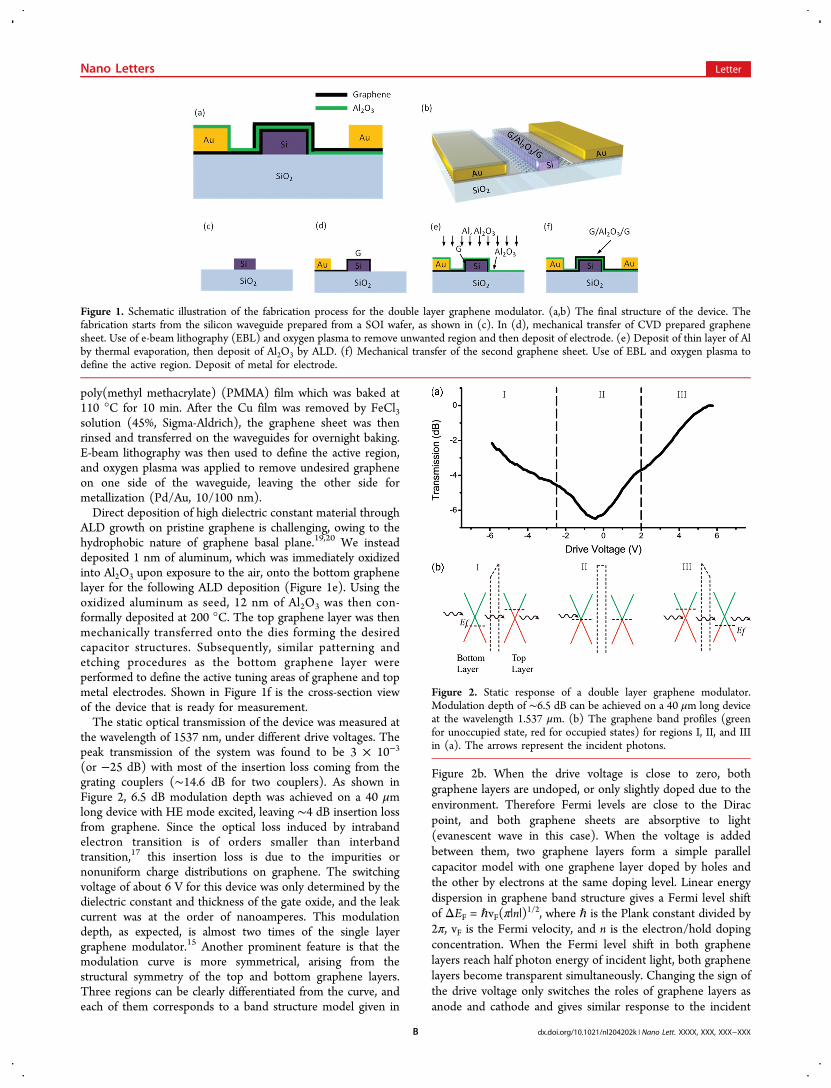
graphene optical modulator. The fabrication starts withcommercial silicon-on-insulator (SOI) wafers with a devicelayer thickness of 340 nm and a buried-oxide thickness of 2 μm.A 400 nm wide silicon waveguide with both ends connected toa pair of grating couplers (period = 780 nm, optimized for λ =1537 nm) were fabricated using deep reactive-ion etch (DRIE).Atomic layer deposition (ALD) technique was then employedto conformally coat a 5 nm thick Al2O3 isolation layer toprevent potential carrier injections from the bottom graphenelayer into the silicon. Chip-sized graphene sheet, prepared onCu film by CVD method,18 was first protected by 200 nm thick
Received: November 29, 2011Revised: January 12, 2012
poly(methyl methacrylate) (PMMA) film which was baked at110 °C for 10 min. After the Cu film was removed by FeCl3solution (45%, Sigma-Aldrich), the graphene sheet was thenrinsed and transferred on the waveguides for overnight baking.E-beam lithography was then used to define the active region,and oxygen plasma was applied to remove undesired grapheneon one side of the waveguide, leaving the other side formetallization (Pd/Au, 10/100 nm).Direct deposition of high dielectric constant material through
ALD growth on pristine graphene is challenging, owing to thehydrophobic nature of graphene basal plane.19,20 We insteaddeposited 1 nm of aluminum, which was immediately oxidizedinto Al2O3 upon exposure to the air, onto the bottom graphenelayer for the following ALD deposition (Figure 1e). Using theoxidized aluminum as seed, 12 nm of Al2O3 was then con-formally deposited at 200 °C. The top graphene layer was thenmechanically transferred onto the dies forming the desiredcapacitor structures. Subsequently, similar patterning andetching procedures as the bottom graphene layer wereperformed to define the active tuning areas of graphene and topmetal electrodes. Shown in Figure 1f is the cross-section viewof the device that is ready for measurement.The static optical transmission of the device was measured at
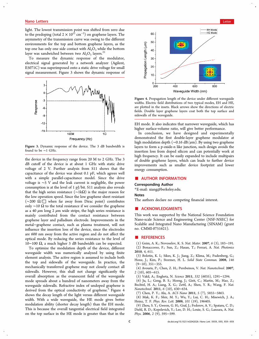
the wavelength of 1537 nm, under different drive voltages. Thepeak transmission of the system was found to be 3 × 10⁻³
(or −25 dB) with most of the insertion loss coming from thegrating couplers (∼14.6 dB for two couplers). As shown inFigure 2, 6.5 dB modulation depth was achieved on a 40 μmlong device with HE mode excited, leaving ∼4 dB insertion lossfrom graphene. Since the optical loss induced by intrabandelectron transition is of orders smaller than interbandtransition,17 this insertion loss is due to the impurities ornonuniform charge distributions on graphene. The switchingvoltage of about 6 V for this device was only determined by thedielectric constant and thickness of the gate oxide, and the leakcurrent was at the order of nanoamperes. This modulationdepth, as expected, is almost two times of the single layergraphene modulator.15 Another prominent feature is that themodulation curve is more symmetrical, arising from thestructural symmetry of the top and bottom graphene layers.Three regions can be clearly differentiated from the curve, andeach of them corresponds to a band structure model given in
Figure 2b. When the drive voltage is close to zero, bothgraphene layers are undoped, or only slightly doped due to theenvironment. Therefore Fermi levels are close to the Diracpoint, and both graphene sheets are absorptive to light(evanescent wave in this case). When the voltage is addedbetween them, two graphene layers form a simple parallelcapacitor model with one graphene layer doped by holes andthe other by electrons at the same doping level. Linear energydispersion in graphene band structure gives a Fermi level shiftof ΔEF = ℏvF(π|n|)
1/2, where ℏ is the Plank constant divided by2π, vF is the Fermi velocity, and n is the electron/hold dopingconcentration. When the Fermi level shift in both graphenelayers reach half photon energy of incident light, both graphenelayers become transparent simultaneously. Changing the sign ofthe drive voltage only switches the roles of graphene layers asanode and cathode and gives similar response to the incident
Figure 1. Schematic illustration of the fabrication process for the double layer graphene modulator. (a,b) The final structure of the device. Thefabrication starts from the silicon waveguide prepared from a SOI wafer, as shown in (c). In (d), mechanical transfer of CVD prepared graphenesheet. Use of e-beam lithography (EBL) and oxygen plasma to remove unwanted region and then deposit of electrode. (e) Deposit of thin layer of Alby thermal evaporation, then deposit of Al2O3 by ALD. (f) Mechanical transfer of the second graphene sheet. Use of EBL and oxygen plasma todefine the active region. Deposit of metal for electrode.
Figure 2. Static response of a double layer graphene modulator.Modulation depth of ∼6.5 dB can be achieved on a 40 μm long deviceat the wavelength 1.537 μm. (b) The graphene band profiles (greenfor unoccupied state, red for occupied states) for regions I, II, and IIIin (a). The arrows represent the incident photons.
Nano Letters Letter
dx.doi.org/10.1021/nl204202k | Nano Lett. XXXX, XXX, XXX−XXXB
light. The lowest transmission point was shifted from zero dueto the predoping (total 2 × 1012 cm−2) on graphene layers. Theasymmetry of the transmission curve was owing to the differentenvironments for the top and bottom graphene layers, as thetop one has only one side contact with Al2O3 while the bottomlayer was sandwiched between two Al2O3 layers.
21
To measure the dynamic response of the modulator,electrical signal generated by a network analyzer (Agilent,E5071C) was superimposed onto a static drive voltage for smallsignal measurement. Figure 3 shows the dynamic response of
the device in the frequency range from 20 M to 2 GHz. The 3dB cutoff of the device is at about 1 GHz with static drivevoltage of 2 V. Further analysis from S11 shows that thecapacitance of the device was about 0.1 pF, which agrees wellwith a simple parallel-capacitance model. Since the drivevoltage is ∼5 V and the leak current is negligible, the powerconsumption is at the level of 1 pJ/bit. S11 analysis also revealsthat the high series resistance (∼1kΩ) is the major reason forthe low operation speed. Since the low graphene sheet resistant(∼200 Ω/□ when far away from Dirac point) contributesonly ∼10 Ω to the total resistance if we consider the grapheneas a 40 μm long 2 μm wide stripe, the high series resistance ismainly contributed from the contact resistance betweengraphene layer and palladium electrode. Improvements in themetal−graphene contact, such as plasma treatment, will notinfluence the insertion loss of the device, since the electrodesare 600 nm away from the active region and do not affect theoptical mode. By reducing the series resistance to the level of10−100 Ω, a much higher 3 dB bandwidth can be expected.To optimize the modulation depth of the device, different
waveguide width was numerically analyzed by using finiteelement analysis. The active region is assumed to include boththe top and sidewalls of the waveguide. In practice, themechanically transferred graphene may not closely contact allsidewalls. However, this shall not change significantly theoverall absorption as the evanescent field of the waveguidemode spreads about a hundred of nanometers away from thewaveguide sidewalls. Refractive index of undoped graphene isderived from the optical conductivity of graphene.5 Figure 4shows the decay length of the light versus different waveguidewidth. With a wide waveguide, the HE mode gives bettermodulation ability (shorter decay length) than the EH mode.This is because the overall tangential electrical field integratedon the top surface in the HE mode is greater than that in the
EH mode. It also indicates that narrower waveguide, which hashigher surface-volume ratio, will give better performance.In conclusion, we have designed and experimentally
demonstrated the first double-layer graphene modulator athigh modulation depth (∼0.16 dB/μm). By using two graphenelayers to form a p-oxide-n like junction, such design avoids theinsertion loss from doped silicon and can potentially work athigh frequency. It can be easily expanded to include multipairsof double graphene layers, which can leads to further deviceimprovements such as smaller device footprint and lowerenergy consumption.
NotesThe authors declare no competing financial interest.
■ ACKNOWLEDGMENTSThis work was supported by the National Science FoundationNano-scale Science and Engineering Center (NSF-NSEC) forScalable and Integrated Nano Manufacturing (SINAM) (grantno. CMMI-0751621).
■ REFERENCES(1) Geim, A. K.; Novoselov, K. S. Nat. Mater. 2007, 6 (3), 183−191.(2) Bonaccorso, F.; Sun, Z.; Hasan, T.; Ferrari, A. Nat. Photonics2010, 4, 611.(3) Bolotin, K. I.; Sikes, K. J.; Jiang, Z.; Klima, M.; Fudenberg, G.;Hone, J.; Kim, P.; Stormer, H. L. Solid State Commun. 2008, 146(9−10), 351−355.(4) Avouris, P.; Chen, Z. H.; Perebeinos, V. Nat. Nanotechnol. 2007,2 (10), 605−615.(5) Vakil, A.; Engheta, N. Science 2011, 332 (6035), 1291−1294.(6) Ju, L.; Geng, B. S.; Horng, J.; Girit, C.; Martin, M.; Hao, Z.;Bechtel, H. A.; Liang, X. G.; Zettl, A.; Shen, Y. R.; Wang, F. Nat.Nanotechnol. 2011, 6 (10), 630−634.(7) Chen, P. Y.; Alu, A. ACS Nano 2011, 5 (7), 5855−5863.(8) Mak, K. F.; Sfeir, M. Y.; Wu, Y.; Lui, C. H.; Misewich, J. A.;Heinz, T. F. Phys. Rev. Lett. 2008, 101 (19), 196405.(9) Zhou, S. Y.; Gweon, G. H.; Graf, J.; Fedorov, A. V.; Spataru, C. D.;Diehl, R. D.; Kopelevich, Y.; Lee, D. H.; Louie, S. G.; Lanzara, A. Nat.Phys. 2006, 2 (9), 595−599.
Figure 3. Dynamic response of the device. The 3 dB bandwidth isfound to be ∼1 GHz.
Figure 4. Propagation length of the device under different waveguidewidths. Electric field distributions of two typical modes, EH and HE,are plotted in the insets. Black arrows show the directions of electricfields. Double layer graphene layers coat both the top surface andsidewalls of the waveguide.
Nano Letters Letter
dx.doi.org/10.1021/nl204202k | Nano Lett. XXXX, XXX, XXX−XXXC
(10) Sun, Z. P.; Popa, D.; Hasan, T.; Torrisi, F.; Wang, F. Q.;Kelleher, E. J. R.; Travers, J. C.; Nicolosi, V.; Ferrari, A. C. Nano Res.2010, 3 (9), 653−660.(11) Bao, Q. L.; Zhang, H.; Wang, B.; Ni, Z. H.; Lim, C. H. Y. X.;Wang, Y.; Tang, D. Y.; Loh, K. P. Nat. Photonics 2011, 5 (7), 411−415.(12) Xia, F. N.; Mueller, T.; Lin, Y. M.; Valdes-Garcia, A.; Avouris, P.Nat. Nanotechnol. 2009, 4 (12), 839−843.(13) Mueller, T.; Xia, F. N. A.; Avouris, P. Nat. Photonics 2010, 4 (5),297−301.(14) Wang, F.; Zhang, Y.; Tian, C.; Girit, C.; Zettl, A.; Crommie, M.;Shen, Y. R. Science 2008, 320 (5873), 206−209.(15) Liu, M.; Yin, X. B.; Ulin-Avila, E.; Geng, B. S.; Zentgraf, T.; Ju,L.; Wang, F.; Zhang, X. Nature 2011, 474 (7349), 64−67.(16) Reed, G. T.; Mashanovich, G.; Gardes, F. Y.; Thomson, D. J.Nat. Photonics 2010, 4 (8), 518−526.(17) Hanson, G. W. J. Appl. Phys. 2008, 103 (6), 064302.(18) Li, X.; Cai, W.; An, J.; Kim, S.; Nah, J.; Yang, D.; Piner, R.;Velamakanni, A.; Jung, I.; Tutuc, E.; Banerjee, S. K.; Colombo, L.;Ruoff, R. S. Science 2009, 324 (5932), 1312−1314.(19) Hollander, M. J.; LaBella, M.; Hughes, Z. R.; Zhu, M.; Trumbull,K. A.; Cavalero, R.; Snyder, D. W.; Wang, X. J.; Hwang, E.; Datta, S.;Robinson, J. A. Nano Lett. 2011, 11 (9), 3601−3607.(20) Kim, S.; Nah, J.; Jo, I.; Shahrjerdi, D.; Colombo, L.; Yao, Z.;Tutuc, E.; Banerjee, S. K. Appl. Phys. Lett. 2009, 94 (6), 062107.(21) Joshi, P.; Romero, H. E.; Neal, A. T.; Toutam, V. K.;Tadigadapa, S. A. J. Phys.: Condens. Matter 2010, 22 (33), 334214 .
Nano Letters Letter
dx.doi.org/10.1021/nl204202k | Nano Lett. XXXX, XXX, XXX−XXXD


![High-Speed Plasmonic-Silicon Modulator Driven by Epsilon ...graphene [5], [6], electro-optic polymer[7], [8], and phase change materials [9]. Such hybrid plasmonic-silicon photonic](https://static.documents.pub/doc/80x56/60bafd81731e884d3b7afae2/high-speed-plasmonic-silicon-modulator-driven-by-epsilon-graphene-5-6.jpg)


![Analysis of an electro-optic modulator based on a graphene …otip.sjtu.edu.cn/publication/Journal/2015-OE-PanTing-Analysis of an... · several tens of micrometers [6, 7], resulting](https://static.documents.pub/doc/80x56/5c41637593f3c338e1322b25/analysis-of-an-electro-optic-modulator-based-on-a-graphene-otipsjtueducnpublicationjournal2015-oe-panting-analysis.jpg)
