18
DPNC Daniel La Marra Activities in the Electronics Group « GrElec »
| Date post: | 16-Dec-2015 |
| Category: |
Documents |
| Upload: | stewart-moore |
| View: | 218 times |
| Download: | 0 times |

DPNC
Daniel La Marra
Activities in theElectronics Group
« GrElec »

218/12/2012 2012 Electronic Highlights
GrElec in 2012
3+1 Electronics Engineers Daniel La Marra Stéphane Débieux Yannick Favre
Alessandro La Rosa• IBL
2 Technical Assistants Gabriel Pelleriti Javier Mesa

2012 Electronic Highlights 318/12/2012
Projects Highlight
ATLAS (LHC) IBL (upgrade phase0 2013-
2014) ABCn130 (upgrade phase2
2022) Neutrinos
MICE (production) Astrophysique
LOFT POLAR
2012 Electronic Highlights 418/12/2012
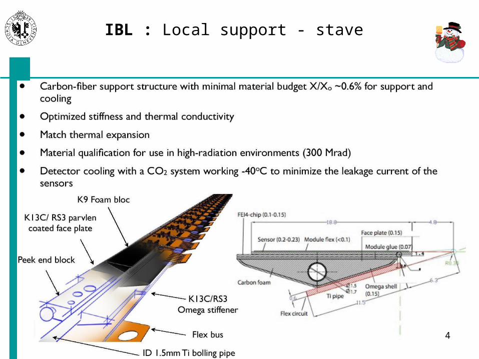
IBL : Local support - stave

2012 Electronic Highlights 518/12/2012
IBL : Dressed module with flex
2012 Electronic Highlights 618/12/2012
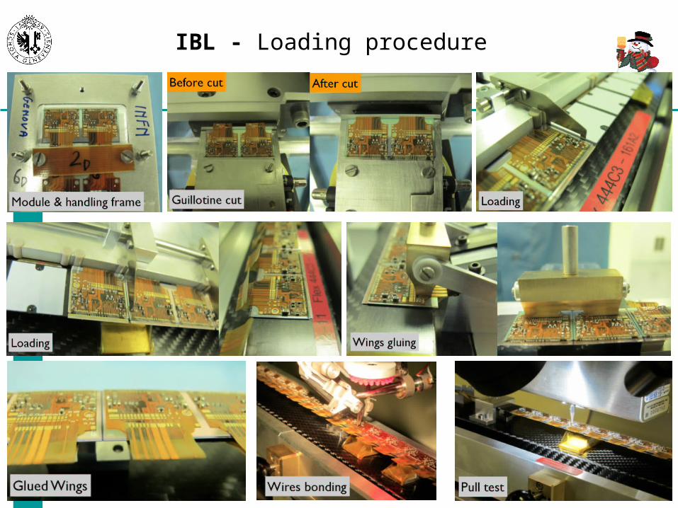
IBL - Loading procedure

2012 Electronic Highlights 7
IBL : Test bench for PCB/Flex Saver production
Purpose : Full production test : ~80 PCB savers, 500 Flex savers Details :
• 320 signals / PCB saver : automatic test for short & open circuit on each signal
• FPGA firmware development for signals stimulus & PC communication (Yannick)
• PC software development for checking & reporting (Yannick) • Test execution (Gaby)
Saver under test
Checked OK for ID=1
PC interface
Flex saversPCB saver
Xilinx Stimulus Board
HW interface18/12/2012

2012 Electronic Highlights 8
IBL : IST & beam pipe EMI qualification
Purpose : Screening qualification against ElectroMagnetic Interference Measurement : Transfer impedance + Screening attenuation vs frequency :
• Tube under test inserted into a copper tube for environment insensitivity• IBL Support Tube (IST) qualification (carbon fiber + Ag glue + end rings)• Beam pipe shielding methods investigation & qualification
Hardware : Vector Network Analyzer [100KHz-4GHz]
IST
Beam PipeVNA
Copper tube enclosure
Good shielding
Bad shielding
Tubes undertest
18/12/2012

918/12/2012 2012 Electronic Highlights
ABCn-130 : Main improvements
ABCn-250 New ABCn-130
Technology: 250nm 130nm
# channels: 128 256
Data rate: 40 Mbit/s 80 Mbit/s
Data flow : Variable Fixed (data rate increase)
TX Chain (chip to chip)
Hardware token signal Software Xon/Xoff (more flexibility)
Single Event Upset Protection
none Configuration choice :- Watchdog or - 3X Flip Flop + vote or- Hamming code
# buffer levels: 1 2 (L0 & L1 triggers)
2012

10
ABCn-130 : Layout (not final) Submission Scenarios
18/12/2012 2012 Electronic Highlights
Chip size 7900 um x 6700 um
Independent of HCC Regular MOSIS MPW on 4th February 2013
(reachable for ABC130, not for HCC) Shared Engineering run with the
NA62/TDCpix submission (forecast 1Q 2013, may be very close to the MOSIS MPW date, but with some flex.)
With HCC : Engineering Run, attached to HCC
schedule
Preferred scenario

DBB : Digitizer & Buffer Board
Context :• MICE experiment (RAL/UK)• Electron Muon Ranger detector (EMR)• Part of a collaborative team with the Front End Board • Board & FPGA design + test : Stéphane Débieux
18/12/2012 2012 Electronic Highlights 11
Mice experiment
EMR
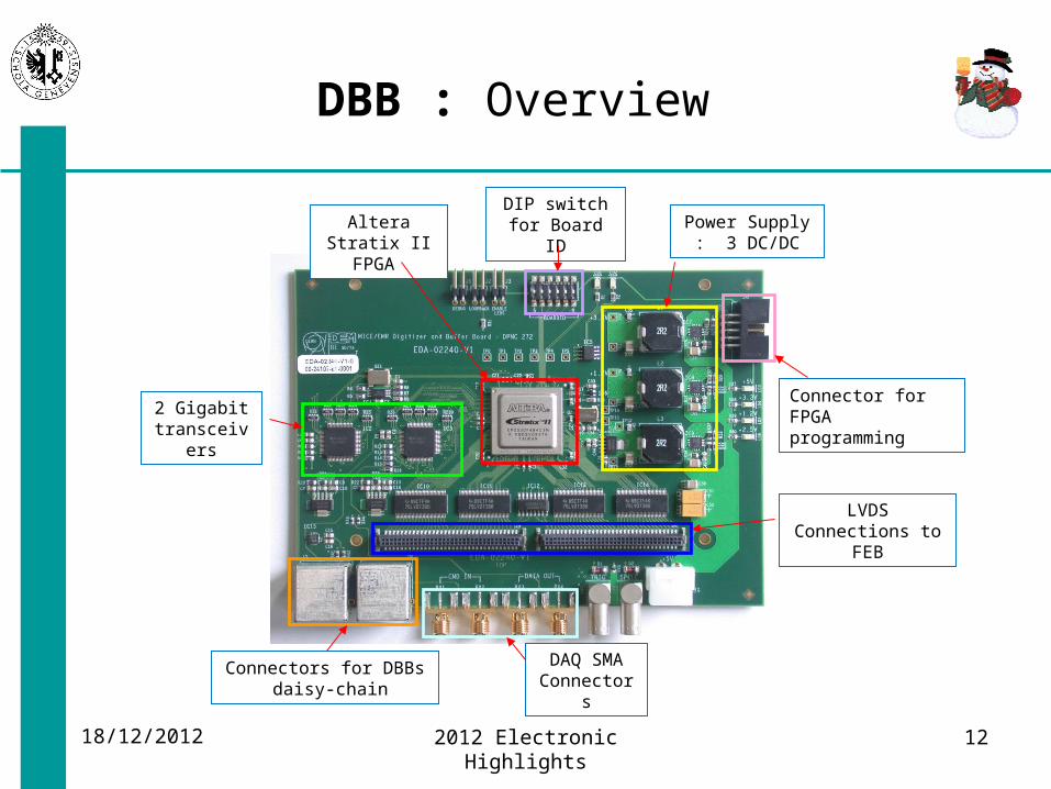
DBB : Overview
18/12/2012 2012 Electronic Highlights 12
2 Gigabit transceivers
Altera Stratix II FPGA
Power Supply : 3 DC/DC
LVDS Connections to FEB
Connectors for DBBs daisy-chain
DAQ SMA Connectors
DIP switch for Board ID
Connector for FPGA programming
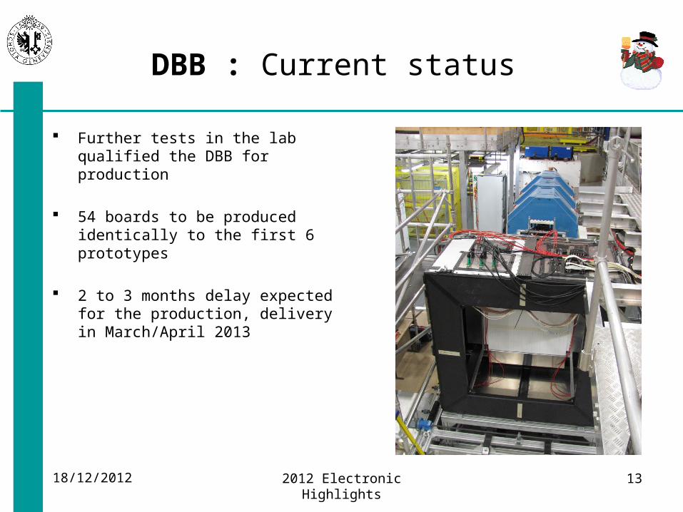
DBB : Current status
18/12/2012 2012 Electronic Highlights 13
Further tests in the lab qualified the DBB for production
54 boards to be produced identically to the first 6 prototypes
2 to 3 months delay expected for the production, delivery in March/April 2013

2012 Electronic Highlights 14
LOFT : Large Observatory For x-ray Timing
Context :• Matter in neutrons Stars & close to black
hole event horizon• ESA program, launch 2020-22• Wide Field Monitor : high resolution• Large Area Detector : 10m² of detector 2-
30keV : 6 panels 7x3 modules/panel 4x4 Front End Electonics/modules => 2016 FEE
overall : DPNC/ISDC design responsibility
FEE :• ~130x70mm• Very low noise• Silicon Drift Detector technology (used in ALICE)• 14 ASICs per FEE, 16 channels/ASIC• Chip On Board technology, very small pads (39µ)• Bonding: ASIC to SDD (17µ), Through PCB Bonds, ASIC to PCB• PCB: Flex-Rigid technology
FEE
Module Back End Electronics
Panel
SDD (bottom)18/12/2012
2012 Electronic Highlights 15
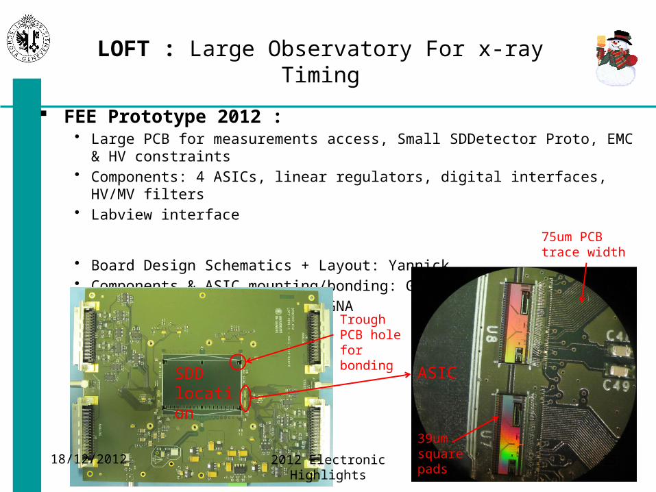
LOFT : Large Observatory For x-ray Timing
FEE Prototype 2012 :• Large PCB for measurements access, Small SDDetector Proto, EMC & HV
constraints• Components: 4 ASICs, linear regulators, digital interfaces, HV/MV filters• Labview interface
• Board Design Schematics + Layout: Yannick• Components & ASIC mounting/bonding: Gaby, Maarten• Tests : in progress at BOLOGNA
SDD location
ASIC
Trough PCB hole for bonding
75um PCB trace width
39um square pads
18/12/2012

2012 Electronic Highlights 16
POLAR : An instrument to measureGamma Ray Bursts polarization
2 layers flex with stiffener:• Design made by PSI• Schematics and Layout was imported into our Cadence tools• Modification with close relationship with the mechanics group• Added a rigid part (stiffener) • Length changed
18/12/2012
2012 Electronic Highlights 17
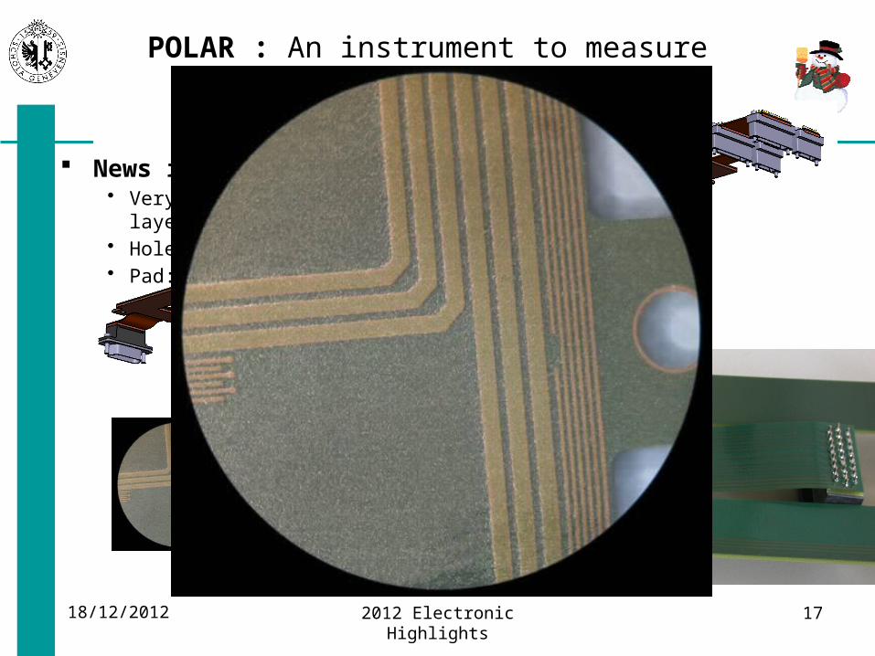
POLAR : An instrument to measureGamma Ray Bursts polarization
18/12/2012
News in this design:• Very small via between 2 layers• Hole: 0.09mm• Pad: 0.15mm

2012 Electronic Highlights 1818/12/2012
Conclusion
This year was going on with some works initiated last year or even before: IBL ABCn130 MICE
There was also new works for several different projects like: LOFT POLAR
But we also started some studies for new projects like: NA61 (neutrinos) DAMPE (astrophysics) JEM-EUSO (astrophysics)


