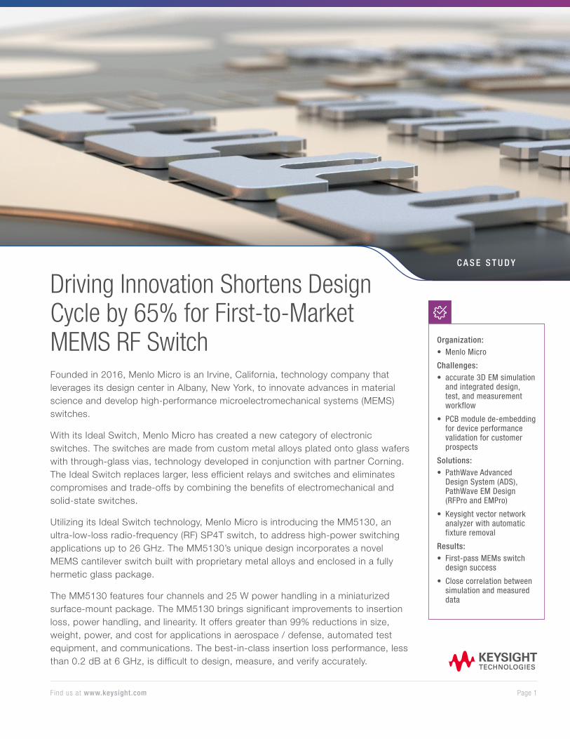
Page 1 Find us at www.keysight.com Driving Innovation Shortens Design Cycle by 65% for First-to-Market MEMS RF Switch Founded in 2016, Menlo Micro is an Irvine, California, technology company that leverages its design center in Albany, New York, to innovate advances in material science and develop high-performance microelectromechanical systems (MEMS) switches. With its Ideal Switch, Menlo Micro has created a new category of electronic switches. The switches are made from custom metal alloys plated onto glass wafers with through-glass vias, technology developed in conjunction with partner Corning. The Ideal Switch replaces larger, less efficient relays and switches and eliminates compromises and trade-offs by combining the benefits of electromechanical and solid-state switches. Utilizing its Ideal Switch technology, Menlo Micro is introducing the MM5130, an ultra-low-loss radio-frequency (RF) SP4T switch, to address high-power switching applications up to 26 GHz. The MM5130’s unique design incorporates a novel MEMS cantilever switch built with proprietary metal alloys and enclosed in a fully hermetic glass package. The MM5130 features four channels and 25 W power handling in a miniaturized surface-mount package. The MM5130 brings significant improvements to insertion loss, power handling, and linearity. It offers greater than 99% reductions in size, weight, power, and cost for applications in aerospace / defense, automated test equipment, and communications. The best-in-class insertion loss performance, less than 0.2 dB at 6 GHz, is difficult to design, measure, and verify accurately. Organization: • Menlo Micro Challenges: • accurate 3D EM simulation and integrated design, test, and measurement workflow • PCB module de-embedding for device performance validation for customer prospects Solutions: • PathWave Advanced Design System (ADS), PathWave EM Design (RFPro and EMPro) • Keysight vector network analyzer with automatic fixture removal Results: • First-pass MEMs switch design success • Close correlation between simulation and measured data CASE STUDY
Transcript
Page 1Find us at www.keysight.com
Driving Innovation Shortens Design Cycle by 65% for First-to-Market MEMS RF SwitchFounded in 2016, Menlo Micro is an Irvine, California, technology company that leverages its design center in Albany, New York, to innovate advances in material science and develop high-performance microelectromechanical systems (MEMS) switches.
With its Ideal Switch, Menlo Micro has created a new category of electronic switches. The switches are made from custom metal alloys plated onto glass wafers with through-glass vias, technology developed in conjunction with partner Corning. The Ideal Switch replaces larger, less efficient relays and switches and eliminates compromises and trade-offs by combining the benefits of electromechanical and solid-state switches.
Utilizing its Ideal Switch technology, Menlo Micro is introducing the MM5130, an ultra-low-loss radio-frequency (RF) SP4T switch, to address high-power switching applications up to 26 GHz. The MM5130’s unique design incorporates a novel MEMS cantilever switch built with proprietary metal alloys and enclosed in a fully hermetic glass package.
The MM5130 features four channels and 25 W power handling in a miniaturized surface-mount package. The MM5130 brings significant improvements to insertion loss, power handling, and linearity. It offers greater than 99% reductions in size, weight, power, and cost for applications in aerospace / defense, automated test equipment, and communications. The best-in-class insertion loss performance, less than 0.2 dB at 6 GHz, is difficult to design, measure, and verify accurately.
Organization:• Menlo Micro
Challenges:• accurate 3D EM simulation
and integrated design, test, and measurement workflow
• PCB module de-embedding for device performance validation for customer prospects
Solutions:• PathWave Advanced
Design System (ADS), PathWave EM Design (RFPro and EMPro)
• Keysight vector network analyzer with automatic fixture removal
Results:• First-pass MEMs switch
design success
• Close correlation between simulation and measured data
C A S E S T U D Y
Page 2Find us at www.keysight.com
Challenge: Proving Best-in-Class Insertion Loss Performance on New TechnologyFor the design and test environment, it was critical to achieve first-pass success from
die-level design to packaged product module, integrated through the application-
level printed circuit board (PCB). This process required an integrated circuit–3D
electromagnetic (EM) design environment to simulate and predict the product
performance at every stage. With an eye on time to market, Menlo targeted a short
design cycle of three to four months for the first product.
Designing the package paths with full 3D EM simulations was critical with an extremely
low-loss RF switch. Menlo needed to design everything, characterizing the modules
with probing and simulating the entire design. Key to customer success was developing
test fixtures and evaluation boards that demonstrate the switch’s actual performance.
Menlo Micro wanted to validate performance early in the development process, so it
chose to implement its own PCB de-embedding algorithms into Keysight’s PathWave
Advanced Design System (ADS) software. After reaching confidence in its simulations,
Menlo created device prototypes and conducted measurements by wafer probing, which
demonstrated first-pass manufacturing success. Then, the engineering team performed
measurements on the vector network analyzer (VNA) to compare its simulation results
against actual de-embedded device measurements as proof of concept for customers.
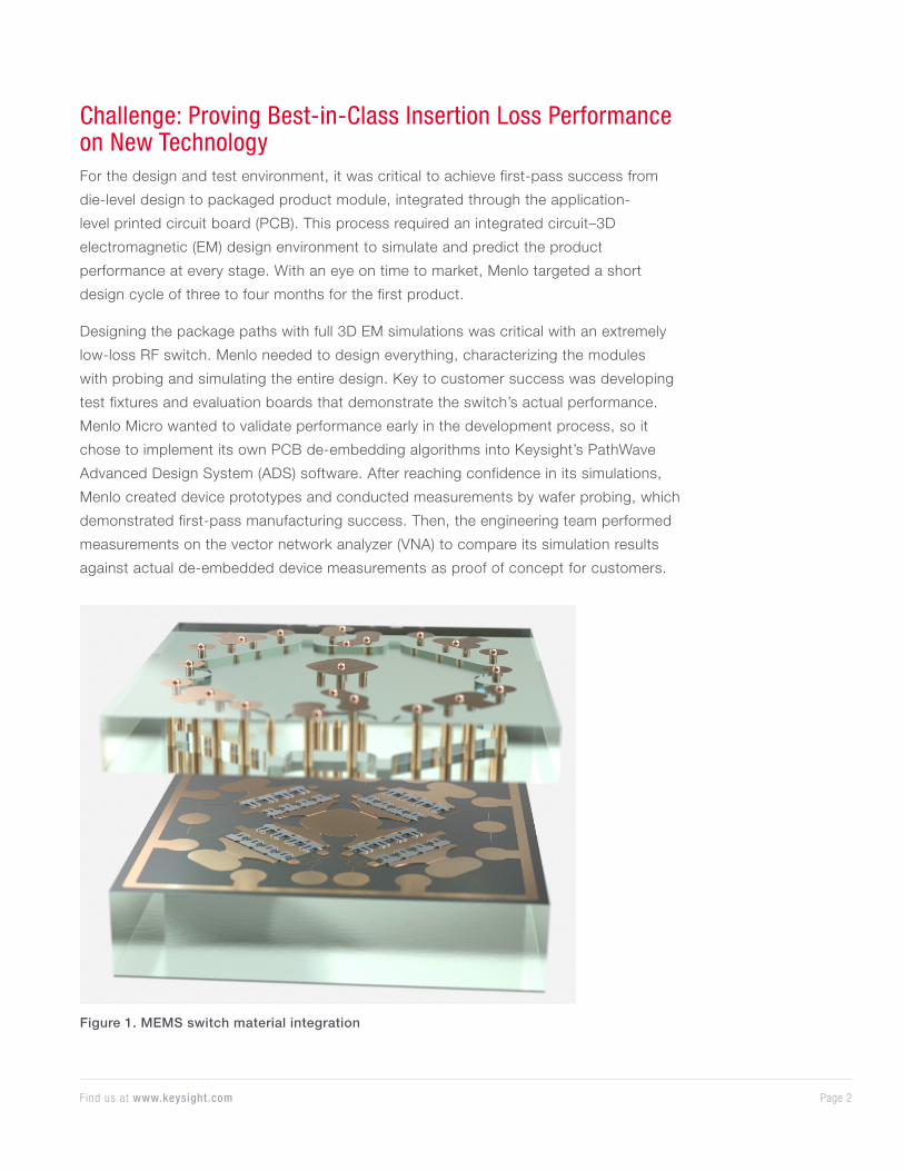
Figure 1. MEMS switch material integration
Page 3Find us at www.keysight.com
Because of the unique material set used (MEMS and PCB) with widely differing
dimensions, Menlo expected significant meshing issues during EM simulation. Menlo uses
metal conductors, plated onto glass substrates, surrounded by an air cavity, with metallic
conductors going through glass to get down through the package and onto the circuit
board. Figure 1 shows the complexity of the material integration.
“One of the challenges is that we have two wafers bonding together,” said Dr. Xu Zhu,
Menlo Micro’s director of technology. “This is a hermetically sealed cavity with a lot of
metal residing on the same level. This created quite a lot of layer meshing issues due to
widely different dimensions. To solve this EM problem in a 3D space, the simulator needs
to cut the 3D space into numerous tiny tetrahedra to resolve the 3D structures and yet not
too many for the EM simulator to handle,” with the MEMS switch sitting on top of a PCB
board several inches in size.
Demonstrating proof of concept
The demonstration of the RF switch performance, with 0.1 or 0.2 dB of loss, is
challenging to measure. The switch must be de-embedded from the evaluation board
to show the end performance in a real-world environment. De-embedding removes the
parasitic effects caused by the surrounding PCB structures and physical connectors.
Making loss measurements on the evaluation board with a VNA adds the parasitic effects
of the evaluation board to the device.
The design stage must include accommodations for de-embedding the performance of
the RF switch from the board to ensure that the results measured on the Keysight PNA
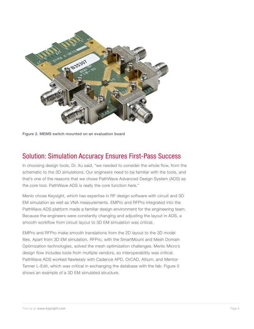
VNA are correlated. Figure 2 shows the switch on the evaluation board. De-embedding
the board design in simulation raises the level of confidence that the device is performing
to specification within the context of the test environment / module. Once manufactured,
the device can be wafer probed to confirm the performance. Then the device is mounted
on the evaluation board, and physical measurements are taken again using the VNA.
An important milestone was the ability to demonstrate proof of concept for early customers.
Neither simulation nor wafer probing results alone are convincing proof of performance;
live measurements on a live demo board are convincing proof of performance. Menlo
Micro has also created several reference designs for use in various applications.
Page 4Find us at www.keysight.com
Figure 2. MEMS switch mounted on an evaluation board
Solution: Simulation Accuracy Ensures First-Pass SuccessIn choosing design tools, Dr. Xu said, “we needed to consider the whole flow, from the
schematic to the 3D simulations. Our engineers need to be familiar with the tools, and
that’s one of the reasons that we chose PathWave Advanced Design System (ADS) as
the core tool. PathWave ADS is really the core function here.”
Menlo chose Keysight, which has expertise in RF design software with circuit and 3D
EM simulation as well as VNA measurements. EMPro and RFPro integrated into the
PathWave ADS platform made a familiar design environment for the engineering team.
Because the engineers were constantly changing and adjusting the layout in ADS, a
smooth workflow from circuit layout to 3D EM simulation was critical.
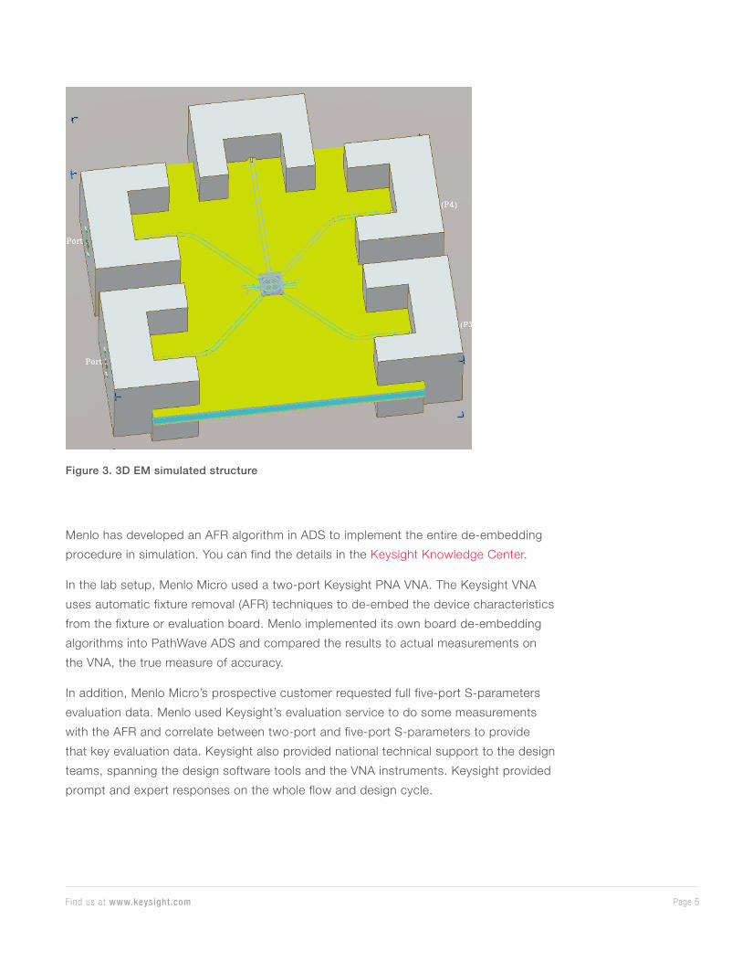
EMPro and RFPro make smooth translations from the 2D layout to the 3D model
files. Apart from 3D EM simulation, RFPro, with the SmartMount and Mesh Domain
Optimization technologies, solved the mesh optimization challenges. Menlo Micro’s
design flow includes tools from multiple vendors, so interoperability was critical.
PathWave ADS worked flawlessly with Cadence APD, OrCAD, Altium, and Mentor-
Tanner L-Edit, which was critical in exchanging the database with the fab. Figure 3
shows an example of a 3D EM simulated structure.
Page 5Find us at www.keysight.com
Menlo has developed an AFR algorithm in ADS to implement the entire de-embedding
procedure in simulation. You can find the details in the Keysight Knowledge Center.
In the lab setup, Menlo Micro used a two-port Keysight PNA VNA. The Keysight VNA
uses automatic fixture removal (AFR) techniques to de-embed the device characteristics
from the fixture or evaluation board. Menlo implemented its own board de-embedding
algorithms into PathWave ADS and compared the results to actual measurements on
the VNA, the true measure of accuracy.
In addition, Menlo Micro’s prospective customer requested full five-port S-parameters
evaluation data. Menlo used Keysight’s evaluation service to do some measurements
with the AFR and correlate between two-port and five-port S-parameters to provide
that key evaluation data. Keysight also provided national technical support to the design
teams, spanning the design software tools and the VNA instruments. Keysight provided
prompt and expert responses on the whole flow and design cycle.
Results: Design Cycle Shortened by 65% with Measurements Correlating Closely to SimulationPrevious projects of this scale lasted up to nine months for a first pass. Careful design
trade-offs and EM simulation / analysis reduced the length of the first pass by 65%.
In comparing the key banner specifications against other alternatives, Menlo Micro
was able to verify that its innovative technology offered significant improvements in the
following areas:
• highest power density (SP4T 25 W power handling)
• lowest RF insertion loss
• best linearity / harmonics
• ultra-low power consumption
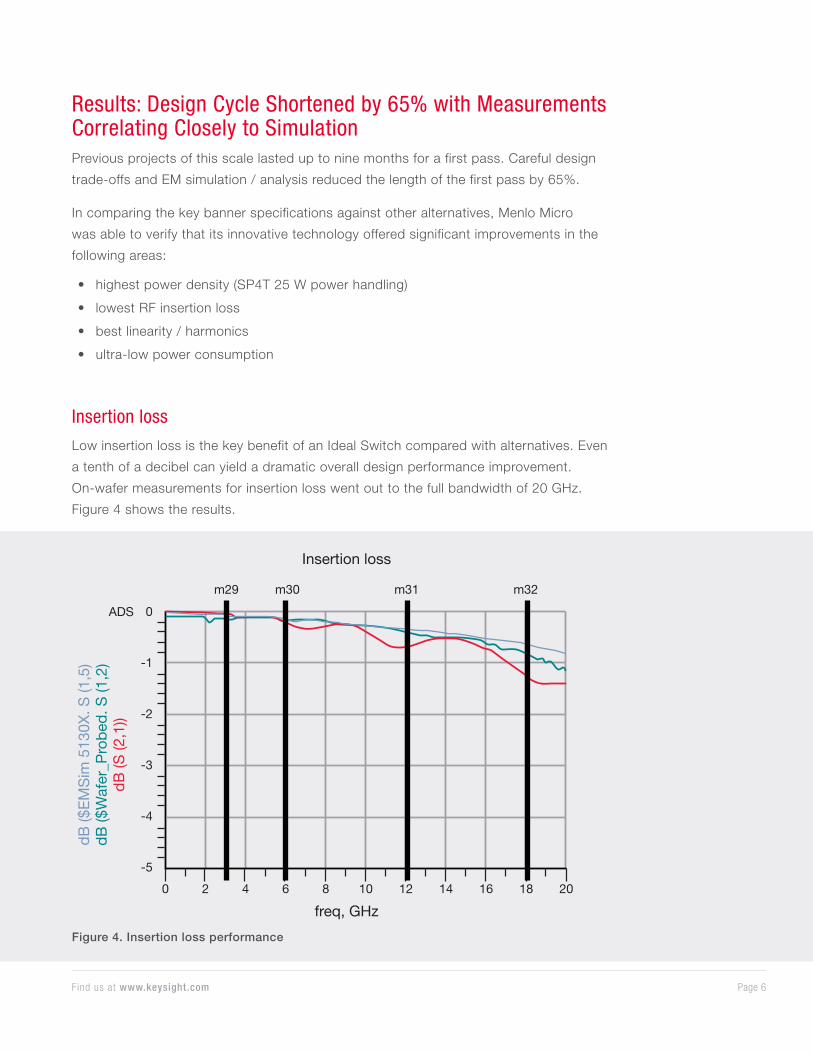
Insertion loss
Low insertion loss is the key benefit of an Ideal Switch compared with alternatives. Even
a tenth of a decibel can yield a dramatic overall design performance improvement.
On-wafer measurements for insertion loss went out to the full bandwidth of 20 GHz.
Figure 4 shows the results.
Figure 4. Insertion loss performance
m29
ADS
freq, GHz
dB ($
EM
Sim
513
0X. S
(1,5
)dB
($W
afer
_Pro
bed.
S (1
,2)
dB (S
(2,1
))
0
-1
-2
m31 m32m30
-3
-4
-5
0 2 4 6 8 10 12 14 16 18 20
Insertion loss
Page 7Find us at www.keysight.com
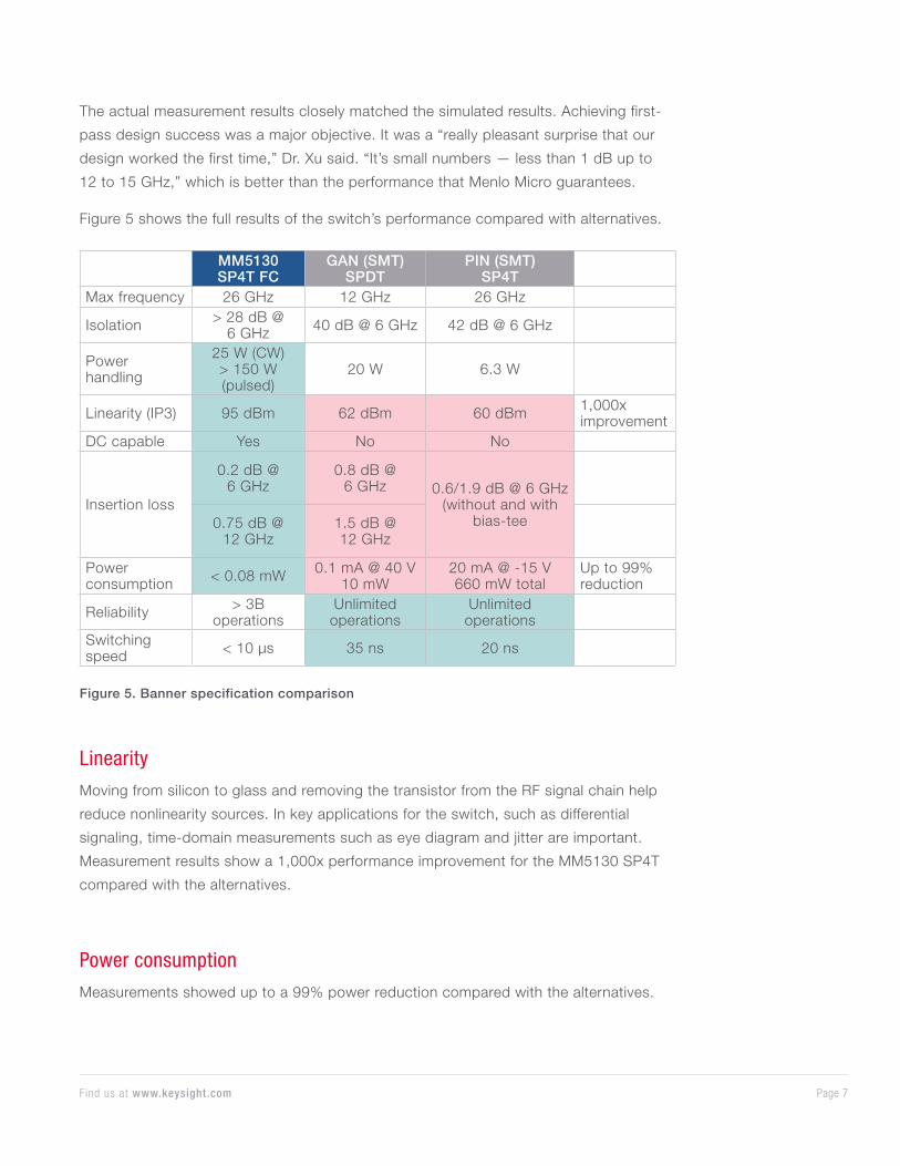
Figure 5. Banner specification comparison
The actual measurement results closely matched the simulated results. Achieving first-
pass design success was a major objective. It was a “really pleasant surprise that our
design worked the first time,” Dr. Xu said. “It’s small numbers — less than 1 dB up to
12 to 15 GHz,” which is better than the performance that Menlo Micro guarantees.
Figure 5 shows the full results of the switch’s performance compared with alternatives.
MM5130 SP4T FC
GAN (SMT) SPDT
PIN (SMT) SP4T
Max frequency 26 GHz 12 GHz 26 GHz
Isolation > 28 dB @ 6 GHz 40 dB @ 6 GHz 42 dB @ 6 GHz
For more information on Keysight Technologies’ products, applications or services,
please contact your local Keysight office. The complete list is available at:
www.keysight.com/find/contactus
Going Forward: Future Plans for 3D EM-Circuit Co-SimulationMenlo recently moved to a subscription software licensing model to access more
capabilities in the short term. The benefits of a subscription model are as follows:
• increased financial flexibility with lower upfront costs and more predictable costs
• flexibility of software mix to accommodate changing market, technology, and methodology needs within each subscription period (available only to enterprise-level agreements)
• simplified software management and deployment
• inclusion of support and software updates
The enterprise package includes RF / microwave system design, 3D EM simulation,
circuit-FEM co-design, high-speed digital, and high-power electronics.
Menlo Micro is increasing the use of the newer RFPro for 3D EM–circuit co-simulation
in ADS to accelerate design and verification and solve meshing issues. RFPro features
a mesh domain optimization capability for the finite element method to automatically
decrease the simulation space when selecting nets or components while keeping an
accurate ground return path.
And finally, Menlo Micro is looking at cloud-based simulation for faster simulation
cycle times. Cloud-based simulations enable easy access to scalable capacity with
cloud processing clusters, particularly useful for large EM simulations. Designing a
complicated 40 Gbps dual DPDT module with more than 5 million tetrahedra takes only