An IMPORTANT NOTICE at the end of this data sheet addresses availability, warranty, changes, use in safety-critical applications,intellectual property matters and other important disclaimers. PRODUCTION DATA.
DRV8871SLVSCY9B –AUGUST 2015–REVISED JULY 2016
DRV8871 3.6-A Brushed DC Motor Driver With Internal Current Sense (PWM Control)
1
1 Features1• H-Bridge Motor Driver
– Drives One DC Motor, One Winding of aStepper Motor, or Other Loads
• Wide 6.5-V to 45-V Operating Voltage• 565-mΩ Typical RDS(on) (HS + LS)• 3.6-A Peak Current Drive• PWM Control Interface• Current Regulation Without a Sense Resistor• Low-Power Sleep Mode• Small Package and Footprint
2 Applications• Printers• Appliances• Industrial Equipment• Other Mechatronic Applications
3 DescriptionThe DRV8871 device is a brushed-DC motor driverfor printers, appliances, industrial equipment, andother small machines. Two logic inputs control the H-bridge driver, which consists of four N-channelMOSFETs that can control motors bidirectionally withup to 3.6-A peak current. The inputs can be pulse-width modulated (PWM) to control motor speed, usinga choice of current-decay modes. Setting both inputslow enters a low-power sleep mode.
The DRV8871 device has advanced current-regulation circuitry that does not use an analogvoltage reference or external sense resistor. Thisnovel solution uses a standard low-cost, low-powerresistor to set the current threshold. The ability to limitcurrent to a known level can significantly reduce thesystem power requirements and bulk capacitanceneeded to maintain stable voltage, especially formotor startup and stall conditions.
The device is fully protected from faults and shortcircuits, including undervoltage (UVLO), overcurrent(OCP), and overtemperature (TSD). When the faultcondition is removed, the device automaticallyresumes normal operation.
Device Information (1)
PART NUMBER PACKAGE BODY SIZE (NOM)DRV8871 HSOP (8) 4.90 mm × 6.00 mm
(1) For all available packages, see the orderable addendum atthe end of the data sheet.
9 Power Supply Recommendations ...................... 149.1 Bulk Capacitance .................................................... 14
10 Layout................................................................... 1510.1 Layout Guidelines ................................................. 1510.2 Layout Example .................................................... 1510.3 Thermal Considerations ........................................ 1510.4 Power Dissipation ................................................. 15
11 Device and Documentation Support ................. 1711.1 Documentation Support ........................................ 1711.2 Receiving Notification of Documentation Updates 1711.3 Community Resources.......................................... 1711.4 Trademarks ........................................................... 1711.5 Electrostatic Discharge Caution............................ 1711.6 Glossary ................................................................ 17
12 Mechanical, Packaging, and OrderableInformation ........................................................... 17
4 Revision HistoryNOTE: Page numbers for previous revisions may differ from page numbers in the current version.
Changes from Revision A (January 2016) to Revision B Page
• Deleted the power supply voltage ramp rate (VM) parameter from the Absolute Maximum Ratings table .......................... 3• Added the output current parameter to the Absolute Maximum Ratings table ...................................................................... 3• Added the Receiving Notification of Documentation Updates section ................................................................................ 17
Changes from Original (August 2015) to Revision A Page
• Updated the ƒPWM max value and added a note .................................................................................................................... 4• Removed the redundant TA condition and added ƒPWM = 24 kHz .......................................................................................... 5• Added more information to clarify how the max RMS current varies for different applications ........................................... 12
GND 1 PWR Logic ground Connect to board groundILIM 4 I Current limit control Connect a resistor to ground to set the current chopping thresholdIN1 3
I Logic inputs Controls the H-bridge output. Has internal pulldowns (see Table 1).IN2 2OUT1 6
O H-bridge output Connect directly to the motor or other inductive load.OUT2 8PGND 7 PWR High-current ground path Connect to board ground.
VM 5 PWR 6.5-V to 45-V powersupply
Connect a 0.1-µF bypass capacitor to ground, as well as sufficientbulk capacitance, rated for the VM voltage.
PAD — — Thermal padConnect to board ground. For good thermal dissipation, use largeground planes on multiple layers, and multiple nearby viasconnecting those planes.
(1) Stresses beyond those listed under Absolute Maximum Ratings may cause permanent damage to the device. These are stress ratingsonly, which do not imply functional operation of the device at these or any other conditions beyond those indicated under RecommendedOperating Conditions. Exposure to absolute-maximum-rated conditions for extended periods may affect device reliability.
6 Specifications
6.1 Absolute Maximum Ratingsover operating free-air temperature range (unless otherwise noted) (1)
MIN MAX UNITPower supply voltage (VM) –0.3 50 VLogic input voltage (IN1, IN2) –0.3 7 VContinuous phase node pin voltage (OUT1, OUT2) –0.7 VM + 0.7 VOutput current (100% duty cycle) 0 3.5 AOperating junction temperature, TJ –40 150 °CStorage temperature, Tstg –65 150 °C
(1) JEDEC document JEP155 states that 500-V HBM allows safe manufacturing with a standard ESD control process.(2) JEDEC document JEP157 states that 250-V CDM allows safe manufacturing with a standard ESD control process.
6.2 ESD RatingsVALUE UNIT
V(ESD) Electrostatic dischargeHuman-body model (HBM), per ANSI/ESDA/JEDEC JS-001 (1) ±6000
VCharged-device model (CDM), per JEDEC specification JESD22-C101 (2) ±750
(1) The voltages applied to the inputs should have at least 800 ns of pulse width to ensure detection. Typical devices require at least400 ns. If the PWM frequency is 200 kHz, the usable duty cycle range is 16% to 84%.
(2) Power dissipation and thermal limits must be observed
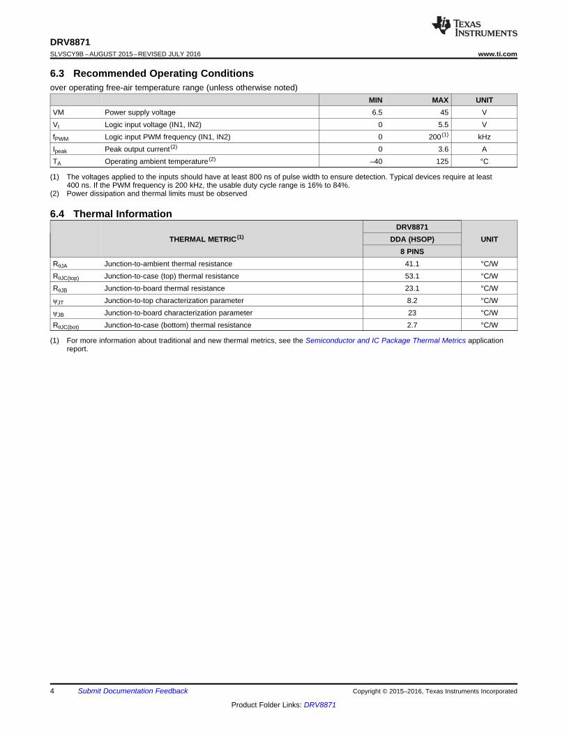
6.3 Recommended Operating Conditionsover operating free-air temperature range (unless otherwise noted)
MIN MAX UNITVM Power supply voltage 6.5 45 VVI Logic input voltage (IN1, IN2) 0 5.5 VfPWM Logic input PWM frequency (IN1, IN2) 0 200 (1) kHzIpeak Peak output current (2) 0 3.6 ATA Operating ambient temperature (2) –40 125 °C
(1) For more information about traditional and new thermal metrics, see the Semiconductor and IC Package Thermal Metrics applicationreport.
PARAMETER TEST CONDITIONS MIN TYP MAX UNITPOWER SUPPLY (VM)VM VM operating voltage 6.5 45 V
IVMVM operating supplycurrent VM = 12 V 3 10 mA
IVMSLEEP VM sleep current VM = 12 V 10 µAtON
(1) Turn-on time VM > VUVLO with IN1 or IN2 high 40 50 µsLOGIC-LEVEL INPUTS (IN1, IN2)VIL Input logic low voltage 0.5 VVIH Input logic high voltage 1.5 VVHYS Input logic hysteresis 0.5 VIIL Input logic low current VIN = 0 V –1 1 μAIIH Input logic high current VIN = 3.3 V 33 100 μARPD Pulldown resistance To GND 100 kΩtPD Propagation delay INx to OUTx change (see Figure 6) 0.7 1 μstsleep Time to sleep Inputs low to sleep 1 1.5 msMOTOR DRIVER OUTPUTS (OUT1, OUT2)
RDS(ON)High-side FET onresistance VM = 24 V, I = 1 A, fPWM = 25 kHz 307 360 mΩ
RDS(ON)Low-side FET onresistance VM = 24 V, I = 1 A, fPWM = 25 kHz 258 320 mΩ
tDEAD Output dead time 220 ns
VdBody diode forwardvoltage IOUT = 1 A 0.8 1 V
CURRENT REGULATION
VILIM
Constant for calculatingcurrent regulation (seeEquation 1)
7.1 OverviewThe DRV8871 device is an optimized 8-pin device for driving brushed DC motors with 6.5 to 45 V and up to 3.6-A peak current. The integrated current regulation restricts motor current to a predefined maximum. Two logicinputs control the H-bridge driver, which consists of four N-channel MOSFETs that have a typical Rds(on) of 565mΩ (including one high-side and one low-side FET). A single power input, VM, serves as both device power andthe motor winding bias voltage. The integrated charge pump of the device boosts VM internally and fullyenhances the high-side FETs. Motor speed can be controlled with pulse-width modulation, at frequenciesbetween 0 to 100 kHz. The device has an integrated sleep mode that is entered by bringing both inputs low. Anassortment of protection features prevent the device from being damaged if a system fault occurs.
7.3.1 Bridge ControlThe DRV8871 output consists of four N-channel MOSFETs that are designed to drive high current. They arecontrolled by the two logic inputs IN1 and IN2, according to Table 1.
Table 1. H-Bridge ControlIN1 IN2 OUT1 OUT2 DESCRIPTION0 0 High-Z High-Z Coast; H-bridge disabled to High-Z (sleep entered after 1 ms)0 1 L H Reverse (Current OUT2 → OUT1)1 0 H L Forward (Current OUT1 → OUT2)1 1 L L Brake; low-side slow decay
The inputs can be set to static voltages for 100% duty cycle drive, or they can be pulse-width modulated (PWM)for variable motor speed. When using PWM, it typically works best to switch between driving and braking. Forexample, to drive a motor forward with 50% of its max RPM, IN1 = 1 and IN2 = 0 during the driving period, andIN1 = 1 and IN2 = 1 during the other period. Alternatively, the coast mode (IN1 = 0, IN2 = 0) for fast currentdecay is also available. The input pins can be powered before VM is applied.
Figure 4. H-Bridge Current Paths
7.3.2 Sleep ModeWhen IN1 and IN2 are both low for time tSLEEP (typically 1 ms), the DRV8871 device enters a low-power sleepmode, where the outputs remain High-Z and the device uses IVMSLEEP (microamps) of current. If the device ispowered up while both inputs are low, sleep mode is immediately entered. After IN1 or IN2 are high for at least 5µs, the device will be operational 50 µs (tON) later.
7.3.3 Current RegulationThe DRV8871 device limits the output current based on a standard resistor attached to pin ILIM, according tothis equation:
For example, if RILIM = 32 kΩ, the DRV8871 device limits motor current to 2 A no matter how much load torque isapplied. The minimum allowed RILIM is 15 kΩ. System designers should always understand the min and maxITRIP, based on the RILIM resistor component tolerance and the DRV8871 specified VILIM range.
When ITRIP has been reached, the device enforces slow current decay by enabling both low-side FETs, and itdoes this for time tOFF (typically 25 µs).
Figure 5. Current Regulation Time Periods
After tOFF has elapsed, the output is re-enabled according to the two inputs INx. The drive time (tDRIVE) untilreaching another ITRIP event heavily depends on the VM voltage, the motor’s back-EMF, and the motor’sinductance.
7.3.4 Dead TimeWhen an output changes from driving high to driving low, or driving low to driving high, dead time is automaticallyinserted to prevent shoot-through. tDEAD is the time in the middle when the output is High-Z. If the output pin ismeasured during tDEAD, the voltage will depend on the direction of current. If current is leaving the pin, thevoltage will be a diode drop below ground. If current is entering the pin, the voltage will be a diode drop aboveVM. This diode is the body diode of the high-side or low-side FET.
7.3.5 Protection CircuitsThe DRV8871 device is fully protected against VM undervoltage, overcurrent, and overtemperature events.
7.3.5.1 VM Undervoltage Lockout (UVLO)If at any time the voltage on the VM pin falls below the undervoltage lockout threshold voltage, all FETs in the H-bridge will be disabled. Operation will resume when VM rises above the UVLO threshold.
7.3.5.2 Overcurrent Protection (OCP)If the output current exceeds the OCP threshold IOCP for longer than tOCP, all FETs in the H-bridge are disabledfor a duration of tRETRY. After that, the H-bridge will be re-enabled according to the state of the INx pins. If theovercurrent fault is still present, the cycle repeats; otherwise normal device operation resumes.
7.3.5.3 Thermal Shutdown (TSD)If the die temperature exceeds safe limits, all FETs in the H-bridge will be disabled. After the die temperature hasfallen to a safe level, operation automatically resumes.
7.4 Device Functional ModesThe DRV8871 device can be used in multiple ways to drive a brushed DC motor.
7.4.1 PWM With Current RegulationThis scheme uses all of the device’s capabilities. ITRIP is set above the normal operating current, and highenough to achieve an adequate spin-up time, but low enough to constrain current to a desired level. Motor speedis controlled by the duty cycle of one of the inputs, while the other input is static. Brake/slow decay is typicallyused during the off-time.
7.4.2 PWM Without Current RegulationIf current regulation is not needed, a 15-kΩ to 18-kΩ resistor should be used on pin ILIM. This mode provides thehighest possible peak current: up to 3.6 A for a few hundred milliseconds (depending on PCB characteristics andthe ambient temperature). If current exceeds 3.6 A, the device might reach overcurrent protection (OCP) orovertemperature shutdown (TSD). If that happens, the device disables and protects itself for about 3 ms (tRETRY)and then resumes normal operation.
7.4.3 Static Inputs With Current RegulationIN1 and IN2 can be set high and low for 100% duty cycle drive, and ITRIP can be used to control the current,speed, and torque capability of the motor.
7.4.4 VM ControlIn some systems it is desirable to vary VM as a means of changing motor speed. See Motor Voltage for moreinformation.
NOTEInformation in the following applications sections is not part of the TI componentspecification, and TI does not warrant its accuracy or completeness. TI’s customers areresponsible for determining suitability of components for their purposes. Customers shouldvalidate and test their design implementation to confirm system functionality.
8.1 Application InformationThe DRV8871 device is typically used to drive one brushed DC motor.
8.2 Typical Application
Figure 7. Typical Connections
8.2.1 Design RequirementsTable 3 lists the design parameters.
Table 3. Design ParametersDESIGN PARAMETER REFERENCE EXAMPLE VALUE
Motor voltage VM 24 VMotor RMS current IRMS 0.8 AMotor startup current ISTART 2 AMotor current trip point ITRIP 2.1 AILIM resistance RILIM 30 kΩPWM frequency fPWM 5 kHz
8.2.2 Detailed Design Procedure
8.2.2.1 Motor VoltageThe motor voltage to use will depend on the ratings of the motor selected and the desired RPM. A higher voltagespins a brushed DC motor faster with the same PWM duty cycle applied to the power FETs. A higher voltagealso increases the rate of current change through the inductive motor windings.
8.2.2.2 Drive CurrentThe current path is through the high-side sourcing DMOS power driver, motor winding, and low-side sinkingDMOS power driver. Power dissipation losses in one source and sink DMOS power driver are shown in thefollowing equation.
The DRV8871 device has been measured to be capable of 2-A RMS current at 25°C on standard FR-4 PCBs.The max RMS current varies based on the PCB design, ambient temperature, and PWM frequency. Typically,switching the inputs at 200 kHz compared to 20 kHz causes 20% more power loss in heat.
8.2.3 Application Curves
Figure 8. Current Ramp With a 2-Ω, 1 mH,RL Load and VM = 12 V
Figure 9. Current Ramp With a 2-Ω, 1 mH,RL Load and VM = 24 V
Figure 10. Current Ramp With a 2-Ω, 1 mH,RL Load and VM = 45 V
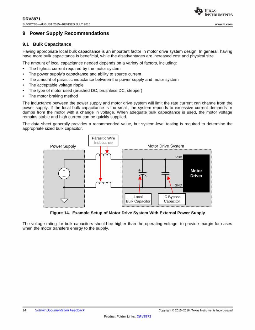
9.1 Bulk CapacitanceHaving appropriate local bulk capacitance is an important factor in motor drive system design. In general, havinghave more bulk capacitance is beneficial, while the disadvantages are increased cost and physical size.
The amount of local capacitance needed depends on a variety of factors, including:• The highest current required by the motor system• The power supply’s capacitance and ability to source current• The amount of parasitic inductance between the power supply and motor system• The acceptable voltage ripple• The type of motor used (brushed DC, brushless DC, stepper)• The motor braking method
The inductance between the power supply and motor drive system will limit the rate current can change from thepower supply. If the local bulk capacitance is too small, the system reponds to excessive current demands ordumps from the motor with a change in voltage. When adequate bulk capacitance is used, the motor voltageremains stable and high current can be quickly supplied.
The data sheet generally provides a recommended value, but system-level testing is required to determine theappropriate sized bulk capacitor.
Figure 14. Example Setup of Motor Drive System With External Power Supply
The voltage rating for bulk capacitors should be higher than the operating voltage, to provide margin for caseswhen the motor transfers energy to the supply.
10.1 Layout GuidelinesThe bulk capacitor should be placed to minimize the distance of the high-current path through the motor driverdevice. The connecting metal trace widths should be as wide as possible, and numerous vias should be usedwhen connecting PCB layers. These practices minimize inductance and allow the bulk capacitor to deliver highcurrent.
Small-value capacitors should be ceramic, and placed closely to device pins.
The high-current device outputs should use wide metal traces.
The device thermal pad should be soldered to the PCB top-layer ground plane. Multiple vias should be used toconnect to a large bottom-layer ground plane. The use of large metal planes and multiple vias help dissipate theI2 × RDS(on) heat that is generated in the device.
10.2 Layout ExampleRecommended layout and component placement is shown in Figure 15
Figure 15. Layout Recommendation
10.3 Thermal ConsiderationsThe DRV8871 device has thermal shutdown (TSD) as described in the Thermal Shutdown (TSD) section. If thedie temperature exceeds approximately 175°C, the device is disabled until the temperature drops below thetemperature hysteresis level.
Any tendency of the device to enter TSD is an indication of either excessive power dissipation, insufficientheatsinking, or too high of an ambient temperature.
10.4 Power DissipationPower dissipation in the DRV8871 device is dominated by the power dissipated in the output FET resistance,RDS(on). Use the equation in the Drive Current section to calculate the estimated average power dissipation whendriving a load.
Note that at startup, the current is much higher than normal running current; this peak current and its durationmust be also be considered.
Power Dissipation (continued)The maximum amount of power that can be dissipated in the device is dependent on ambient temperature andheatsinking.
NOTERDS(on) increases with temperature, so as the device heats, the power dissipationincreases. This fact must be taken into consideration when sizing the heatsink.
The power dissipation of the DRV8871 device is a function of RMS motor current and the FET resistance(RDS(ON)) of each output.
(3)
For this example, the ambient temperature is 58°C, and the junction temperature reaches 80°C. At 58°C, thesum of RDS(ON) is about 0.72 Ω. With an example motor current of 0.8 A, the dissipated power in the form of heatwill be 0.8 A2 × 0.72 Ω = 0.46 W.
The temperature that the DRV8871 device reaches depends on the thermal resistance to the air and PCB. It isimportant to solder the device PowerPAD to the PCB ground plane, with vias to the top and bottom board layers,in order dissipate heat into the PCB and reduce the device temperature. In the example used here, the DRV8871device had an effective thermal resistance RθJA of 48°C/W, and:
(4)
10.4.1 HeatsinkingThe PowerPAD package uses an exposed pad to remove heat from the device. For proper operation, this padmust be thermally connected to copper on the PCB to dissipate heat. On a multi-layer PCB with a ground plane,this connection can be accomplished by adding a number of vias to connect the thermal pad to the ground plane.
On PCBs without internal planes, a copper area can be added on either side of the PCB to dissipate heat. If thecopper area is on the opposite side of the PCB from the device, thermal vias are used to transfer the heatbetween top and bottom layers.
For details about how to design the PCB, refer to the TI application report, PowerPAD™ Thermally EnhancedPackage, and the TI application brief, PowerPAD Made Easy™, available at www.ti.com. In general, the morecopper area that can be provided, the more power can be dissipated.
11.1.1 Related DocumentationFor related documentation, see the following:• Current Recirculation and Decay Modes• Calculating Motor Driver Power Dissipation• DRV8871 Evaluation Module• PowerPAD™ Thermally Enhanced Package• PowerPAD™ Made Easy• Understanding Motor Driver Current Ratings
11.2 Receiving Notification of Documentation UpdatesTo receive notification of documentation updates, navigate to the device product folder on ti.com. In the upperright corner, click on Alert me to register and receive a weekly digest of any product information that haschanged. For change details, review the revision history included in any revised document.
11.3 Community ResourcesThe following links connect to TI community resources. Linked contents are provided "AS IS" by the respectivecontributors. They do not constitute TI specifications and do not necessarily reflect TI's views; see TI's Terms ofUse.
TI E2E™ Online Community TI's Engineer-to-Engineer (E2E) Community. Created to foster collaborationamong engineers. At e2e.ti.com, you can ask questions, share knowledge, explore ideas and helpsolve problems with fellow engineers.
Design Support TI's Design Support Quickly find helpful E2E forums along with design support tools andcontact information for technical support.
11.4 TrademarksPowerPAD, E2E are trademarks of Texas Instruments.All other trademarks are the property of their respective owners.
11.5 Electrostatic Discharge CautionThese devices have limited built-in ESD protection. The leads should be shorted together or the device placed in conductive foamduring storage or handling to prevent electrostatic damage to the MOS gates.
11.6 GlossarySLYZ022 — TI Glossary.
This glossary lists and explains terms, acronyms, and definitions.
12 Mechanical, Packaging, and Orderable InformationThe following pages include mechanical, packaging, and orderable information. This information is the mostcurrent data available for the designated devices. This data is subject to change without notice and revision ofthis document. For browser-based versions of this data sheet, refer to the left-hand navigation.
Texas Instruments Incorporated and its subsidiaries (TI) reserve the right to make corrections, enhancements, improvements and otherchanges to its semiconductor products and services per JESD46, latest issue, and to discontinue any product or service per JESD48, latestissue. Buyers should obtain the latest relevant information before placing orders and should verify that such information is current andcomplete. All semiconductor products (also referred to herein as “components”) are sold subject to TI’s terms and conditions of salesupplied at the time of order acknowledgment.TI warrants performance of its components to the specifications applicable at the time of sale, in accordance with the warranty in TI’s termsand conditions of sale of semiconductor products. Testing and other quality control techniques are used to the extent TI deems necessaryto support this warranty. Except where mandated by applicable law, testing of all parameters of each component is not necessarilyperformed.TI assumes no liability for applications assistance or the design of Buyers’ products. Buyers are responsible for their products andapplications using TI components. To minimize the risks associated with Buyers’ products and applications, Buyers should provideadequate design and operating safeguards.TI does not warrant or represent that any license, either express or implied, is granted under any patent right, copyright, mask work right, orother intellectual property right relating to any combination, machine, or process in which TI components or services are used. Informationpublished by TI regarding third-party products or services does not constitute a license to use such products or services or a warranty orendorsement thereof. Use of such information may require a license from a third party under the patents or other intellectual property of thethird party, or a license from TI under the patents or other intellectual property of TI.Reproduction of significant portions of TI information in TI data books or data sheets is permissible only if reproduction is without alterationand is accompanied by all associated warranties, conditions, limitations, and notices. TI is not responsible or liable for such altereddocumentation. Information of third parties may be subject to additional restrictions.Resale of TI components or services with statements different from or beyond the parameters stated by TI for that component or servicevoids all express and any implied warranties for the associated TI component or service and is an unfair and deceptive business practice.TI is not responsible or liable for any such statements.Buyer acknowledges and agrees that it is solely responsible for compliance with all legal, regulatory and safety-related requirementsconcerning its products, and any use of TI components in its applications, notwithstanding any applications-related information or supportthat may be provided by TI. Buyer represents and agrees that it has all the necessary expertise to create and implement safeguards whichanticipate dangerous consequences of failures, monitor failures and their consequences, lessen the likelihood of failures that might causeharm and take appropriate remedial actions. Buyer will fully indemnify TI and its representatives against any damages arising out of the useof any TI components in safety-critical applications.In some cases, TI components may be promoted specifically to facilitate safety-related applications. With such components, TI’s goal is tohelp enable customers to design and create their own end-product solutions that meet applicable functional safety standards andrequirements. Nonetheless, such components are subject to these terms.No TI components are authorized for use in FDA Class III (or similar life-critical medical equipment) unless authorized officers of the partieshave executed a special agreement specifically governing such use.Only those TI components which TI has specifically designated as military grade or “enhanced plastic” are designed and intended for use inmilitary/aerospace applications or environments. Buyer acknowledges and agrees that any military or aerospace use of TI componentswhich have not been so designated is solely at the Buyer's risk, and that Buyer is solely responsible for compliance with all legal andregulatory requirements in connection with such use.TI has specifically designated certain components as meeting ISO/TS16949 requirements, mainly for automotive use. In any case of use ofnon-designated products, TI will not be responsible for any failure to meet ISO/TS16949.
Products ApplicationsAudio www.ti.com/audio Automotive and Transportation www.ti.com/automotiveAmplifiers amplifier.ti.com Communications and Telecom www.ti.com/communicationsData Converters dataconverter.ti.com Computers and Peripherals www.ti.com/computersDLP® Products www.dlp.com Consumer Electronics www.ti.com/consumer-appsDSP dsp.ti.com Energy and Lighting www.ti.com/energyClocks and Timers www.ti.com/clocks Industrial www.ti.com/industrialInterface interface.ti.com Medical www.ti.com/medicalLogic logic.ti.com Security www.ti.com/securityPower Mgmt power.ti.com Space, Avionics and Defense www.ti.com/space-avionics-defenseMicrocontrollers microcontroller.ti.com Video and Imaging www.ti.com/videoRFID www.ti-rfid.comOMAP Applications Processors www.ti.com/omap TI E2E Community e2e.ti.comWireless Connectivity www.ti.com/wirelessconnectivity