Supporting Information
Boundary Layer Effect on Solvent Evaporation during Perovskite Film
Drying by Multi-flow Air Knife
Li-Li Gao, Ke-Jie Zhang, Chen Ni and Guan-Jun Yang*
School of Materials Science and Engineering, Xi’an Jiaotong University, Xi’an, Shaanxi 710049, P.R. China
* E-mail: [email protected]
Experimental section
Materials preparation
Lead iodide (PbI2, 99.99%), N,N-dimethylformamide (DMF, 99.8%), iodine methylamine (CH3NH3I) were purchased
from Xi'an Polymer Light Technology Corp., and used as received. Titanium dioxide precursor solvent was
synthesized following the reported procedure.1 Spiro-MeOTAD solution was prepared according to the report.2 It
was prepared by dissolving 72.3 mg of spiro-MeOTAD in 1 ml of chlorobenzene, to which 28.8 μl of 4-tert-
butylpyridine and 17.5 μl of lithiumbis(trifluoromethanesulfonyl)imide(Li-TFSI) solution (520 mg LI-TSFI in 1 ml
acetonitrile, Sigma-Aldrich, 99.8%) were added.
Perovskite film fabrication
The perovskite precursor solution was composed of PbI2 and CH3NH3I at a molar ratio of 1:1, which dissolved in
DMF solvent at 70 oC and stirred for 12 h. An appropriate amount of perovskite precursor solution was dropped
on the TiO2-coated FTO surface and spinned at 5000 rpm for 6 s, a light yellow liquid perovskite precursor film of
~3 μm in thickness was obtained. Subsequently, MAK swept across the solution film at various air flow rates and
air temperatures. In this study, we adopted the flow rate values of 50, 150, 250 and 350 L min−1, using several
different air temperatures, 20, 50, 100, 150oC. The dried films were annealed for 10 min at 100 °C on a hot plate.
Perovskite Solar Cell Fabrication
Devices were fabricated on Fluorine-doped tin oxide (FTO) coated glass (Pilkington, 15 Ω sq−1). The FTO substrates
were cut into 25 mm × 25 mm pieces and rinsed sequentially with acetone, ethyl alcohol, and deionized water in
an ultrasonic bath for 10 min, and then blow dried by nitrogen. The FTO substrates were treated with ozone and
ultraviolet light for 15 min for increasing wettability. TiO2 was deposited by spin coating at 4500 rpm for 30 s as
the electron transport layer of compact, and sintered at 500°C for 30 min. The dense TiO2 layer was ~50 nm thick.
A compact 300 nm thick perovskite film, as the light absorption layer, was deposited by MAK method on the TiO2
layer. All above steps were conducted under ambient conditions at the temperature of 20 °C and humidity of 30%.
About 20 μL spiro-OMeTAD solution was spin coated on perovskite films at 4000 rpm for 30 s. Then it was left
overnight to allow for the spiro-OMeTAD doping via oxidation in a drying box with humidity of 13%. Finally, an 80-
Electronic Supplementary Material (ESI) for Journal of Materials Chemistry A.This journal is © The Royal Society of Chemistry 2017
nm-thick Au layer was deposited by thermal evaporation under vacuum of 4 × 10⁻⁴ Pa. The finished device was
stored in a N2-purged glovebox (<0.1 ppm O2 and H2O) before measurement.
Measurement and Characterization
The XRD patterns of the FTO substrate and perovskite film were obtained with a D8 Advance X-ray diffractometer
with Cu K radiation. All samples were scanned from 10° to 60° with a step size of 0.2°. The absorption spectra of
the perovskite films were measured with a U-3010 spectrophotometer. The surface morphologies of the perovskite
films were examined using SEM (VEGA II-XMU, TESCAN, Czech Republic). AFM (Veeco diInnova, Bruker, America)
was used to examine the surface profile and roughness. J–V curves of the perovskite solar cells were measured
using a Keithley 2400 source-measure unit under the illumination of simulated sunlight, provided by a 450 W Class
AAA solar simulator equipped with a filtered Xe lamp, (AM 1.5G, 100 mW cm−2, Sol3A, Oriel Instruments). The
output light intensity was calibrated using a single-crystal silicon photovoltaic cell as the reference (91150V, Oriel
Instruments). The cells were measured with a non-reflective metal mask covering areas of 1 and 0.1 cm2 to receive
sunlight and avoid light scattering through the edges. The current densities of the devices were measured by
biasing the devices at maximum power point for 150 s, and then calculating the steady-state power conversion
efficiency by multiply steady-state current densities and maximum biasing. IPCE spectra of the device was tested
in air without bias light by using a Qtest Station 1000ADX system (Growntech, Inc.). The illumination spot size was
slightly smaller than the active area of the test cells. IPCE photocurrents were recorded under short-circuit
conditions using a Keithley 2400 source meter. The monochromatic photon flux was quantified by means of a
calibrated silicon photodiode. Electrochemical impedance spectroscopy (EIS) analysis was conducted on a ZAHNER
ENNIUM Electrochemical Workstation.
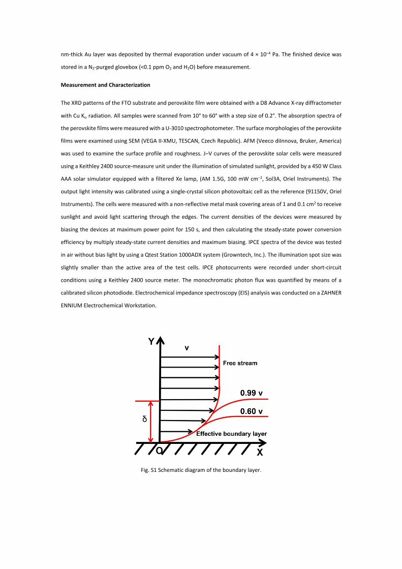
Fig. S1 Schematic diagram of the boundary layer.
Fig. S2 Grain size distribution of perovskite grains.
Fig. S3 (a) Absorbance spectrum of perovskite film dried by multi-flow air knife, (b) absorbance, transmission, and
reflection percentage of perovskite film dried by multi-flow air knife.
Fig. S4 Air density and viscosity variation tendency along temperature increasing.
Fig. S5 Schematic diagram of one unit multi-flow air knife drying (a), simulation mash (b).
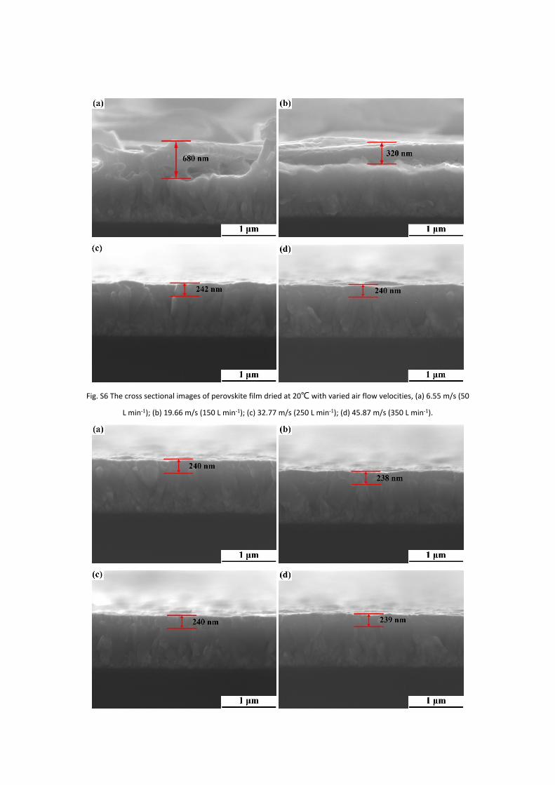
Fig. S6 The cross sectional images of perovskite film dried at 20℃ with varied air flow velocities, (a) 6.55 m/s (50
L min-1); (b) 19.66 m/s (150 L min-1); (c) 32.77 m/s (250 L min-1); (d) 45.87 m/s (350 L min-1).
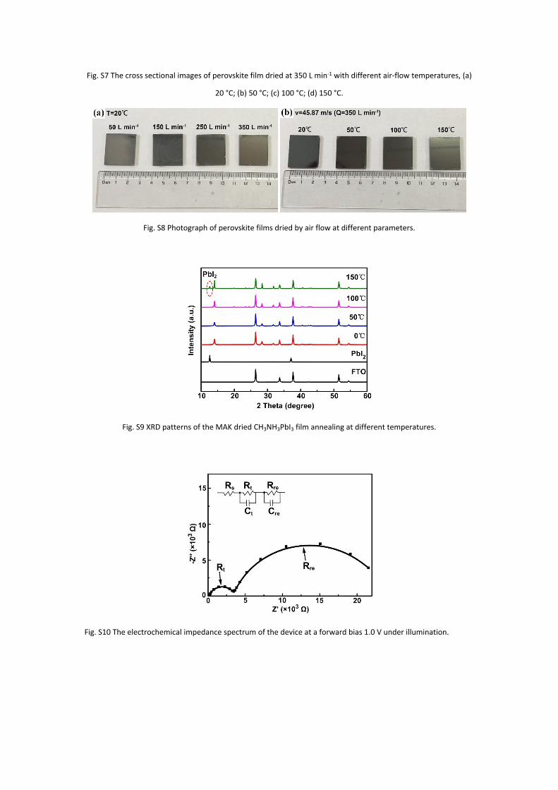
Fig. S7 The cross sectional images of perovskite film dried at 350 L min-1 with different air-flow temperatures, (a)
20 °C; (b) 50 °C; (c) 100 °C; (d) 150 °C.
Fig. S8 Photograph of perovskite films dried by air flow at different parameters.
Fig. S9 XRD patterns of the MAK dried CH3NH3PbI3 film annealing at different temperatures.
Fig. S10 The electrochemical impedance spectrum of the device at a forward bias 1.0 V under illumination.
Fig. S11 J−V curves of the device with different condition perovskite films, (a) films dried by various air velocities
at 20 oC, (b)films dried by various air temperatures at 45.87 m/s (350 L min-1), (c) films annealed at different
temperatures for 10 min.
Fig. S12 (a) IPCE spectra of the device with active area of 0.1 cm2, (b) XRD patterns of the MAK dried perovskite
film measured at different moment.
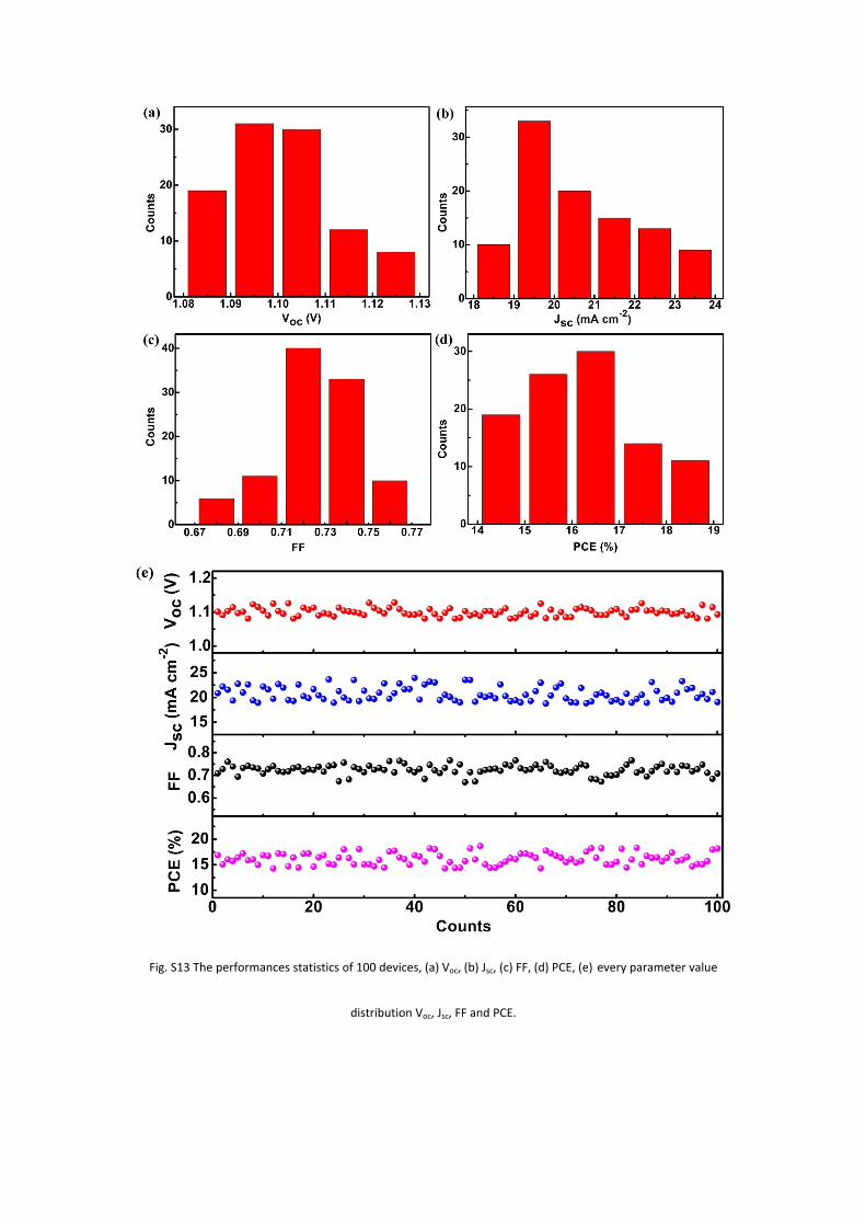
Fig. S13 The performances statistics of 100 devices, (a) Voc, (b) Jsc, (c) FF, (d) PCE, (e) every parameter value
distribution Voc, Jsc, FF and PCE.
Table S1 Boundary layer thickness with varied air temperatures and varied air velocities. Here, L=d=0.025 m. All air
velocity is consisted with an air flow, which can be tuned mechanically.
T (oC) ρ (kg/m3) η (×10-5 Pa·s) v (m/s) Q (L min-1) δ(μm)
20℃ 1.205 1.81 6.55 50 239.4
20℃ 1.205 1.81 19.66 150 138.2
20℃ 1.205 1.81 32.77 250 107.0
20℃ 1.205 1.81 45.87 350 90.5
50℃ 1.093 1.96 6.55 50 261.6
50℃ 1.093 1.96 19.66 150 151.0
50℃ 1.093 1.96 32.77 250 116.9
50℃ 1.093 1.96 45.87 350 98.9
100℃ 0.946 2.19 6.55 50 297.3
100℃ 0.946 2.19 19.66 150 171.6
100℃ 0.946 2.19 32.77 250 132.9
100℃ 0.946 2.19 45.87 350 112.3
150℃ 0.835 2.41 6.55 50 331.9
150℃ 0.835 2.41 19.66 150 191.6
150℃ 0.835 2.41 32.77 250 148.4
150℃ 0.835 2.41 45.87 350 125.4
1. Li, N.; Dong, H.; Dong, H.; Li, J.; Li, W.; Niu, G.; Guo, X.; Wu, Z.; Wang, L., Multifunctional perovskite capping
layers in hybrid solar cells. J Mater Chem A 2014, 2 (36), 14973.
2. Im, J. H.; Jang, I. H.; Pellet, N.; Gratzel, M.; Park, N. G., Growth of CH3NH3PbI3 cuboids with controlled size for
high-efficiency perovskite solar cells. Nat Nanotechnol 2014, 9 (11), 927-932.