Receive Equalization Eliminate Data DESCRIPTIONDependant Jitter The DS25CP102 is a 3.125 Gbps 2x2 LVDS
• Wide Input Common Mode Voltage Range crosspoint switch optimized for high-speed signalrouting and switching over lossy FR-4 printed circuitAllows DC-Coupled Interface to CML andboard backplanes and balanced cables. FullyLVPECL Driversdifferential signal paths ensure exceptional signal• On-Chip 100Ω Input and Output Terminationintegrity and noise immunity. The non-blocking
Minimizes Insertion and Return Losses, architecture allows connections of any input to anyReduces Component Count, Minimizes Board output or outputs.Space
The DS25CP102 features two levels (Off and On) of• 8 kV ESD on LVDS I/O Pins Protects Adjoining transmit pre-emphasis (PE) and two levels (Off andComponents On) of receive equalization (EQ).
• Small 4 mm x 4 mm WQFN-16 Space SavingWide input common mode range allows the switch toPackageaccept signals with LVDS, CML and LVPECL levels;the output levels are LVDS. A very small packagefootprint requires a minimal space on the board whilethe flow-through pinout allows easy board layout.Each differential input and output is internallyterminated with a 100Ω resistor to lower deviceinsertion and return losses, reduce component countand further minimize board space.
1
Please be aware that an important notice concerning availability, standard warranty, and use in critical applications ofTexas Instruments semiconductor products and disclaimers thereto appears at the end of this data sheet.
2All trademarks are the property of their respective owners.
www.ti.com SNLS262E –OCTOBER 2007–REVISED MARCH 2013
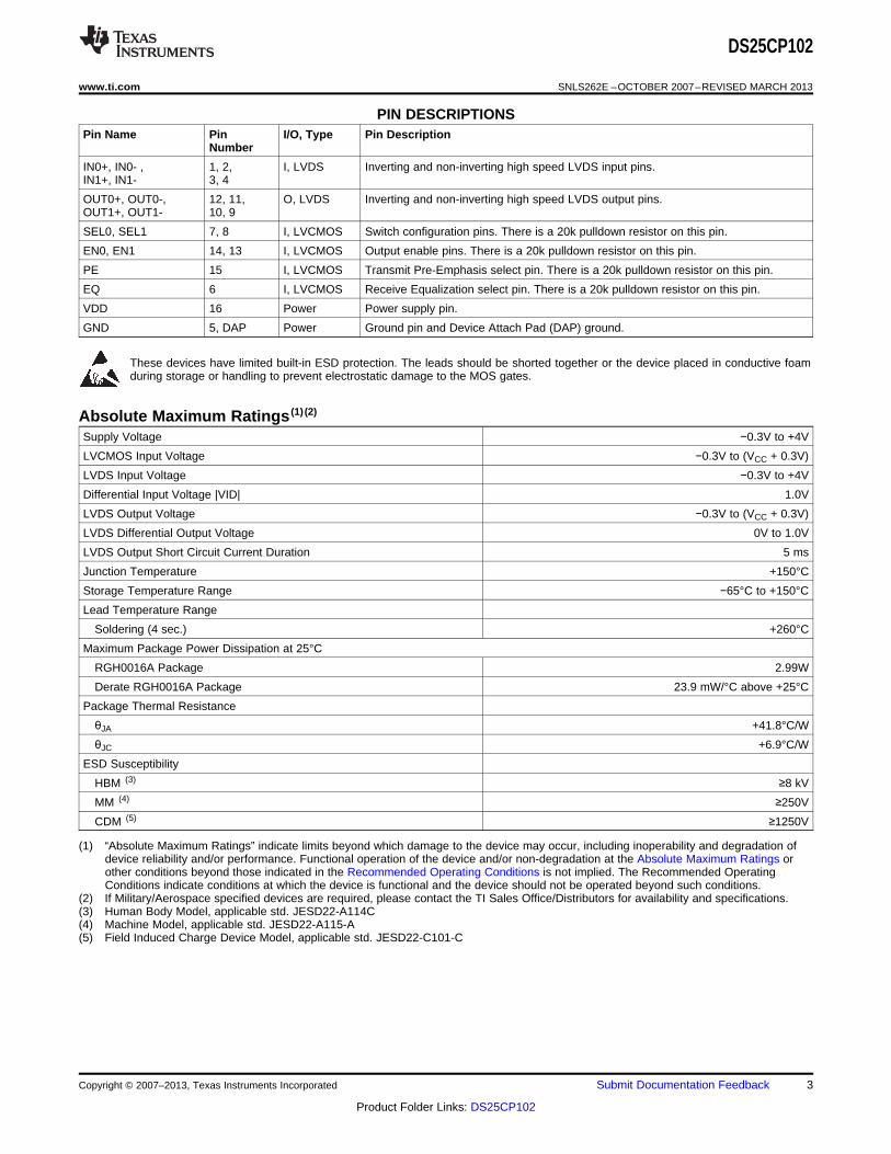
PIN DESCRIPTIONSPin Name Pin I/O, Type Pin Description
Number
IN0+, IN0- , 1, 2, I, LVDS Inverting and non-inverting high speed LVDS input pins.IN1+, IN1- 3, 4
OUT0+, OUT0-, 12, 11, O, LVDS Inverting and non-inverting high speed LVDS output pins.OUT1+, OUT1- 10, 9
SEL0, SEL1 7, 8 I, LVCMOS Switch configuration pins. There is a 20k pulldown resistor on this pin.
EN0, EN1 14, 13 I, LVCMOS Output enable pins. There is a 20k pulldown resistor on this pin.
PE 15 I, LVCMOS Transmit Pre-Emphasis select pin. There is a 20k pulldown resistor on this pin.
EQ 6 I, LVCMOS Receive Equalization select pin. There is a 20k pulldown resistor on this pin.
VDD 16 Power Power supply pin.
GND 5, DAP Power Ground pin and Device Attach Pad (DAP) ground.
These devices have limited built-in ESD protection. The leads should be shorted together or the device placed in conductive foamduring storage or handling to prevent electrostatic damage to the MOS gates.
Absolute Maximum Ratings (1) (2)
Supply Voltage −0.3V to +4V
LVCMOS Input Voltage −0.3V to (VCC + 0.3V)
LVDS Input Voltage −0.3V to +4V
Differential Input Voltage |VID| 1.0V
LVDS Output Voltage −0.3V to (VCC + 0.3V)
LVDS Differential Output Voltage 0V to 1.0V
LVDS Output Short Circuit Current Duration 5 ms
Junction Temperature +150°C
Storage Temperature Range −65°C to +150°C
Lead Temperature Range
Soldering (4 sec.) +260°C
Maximum Package Power Dissipation at 25°C
RGH0016A Package 2.99W
Derate RGH0016A Package 23.9 mW/°C above +25°C
Package Thermal Resistance
θJA +41.8°C/W
θJC +6.9°C/W
ESD Susceptibility
HBM (3) ≥8 kV
MM (4) ≥250V
CDM (5) ≥1250V
(1) “Absolute Maximum Ratings” indicate limits beyond which damage to the device may occur, including inoperability and degradation ofdevice reliability and/or performance. Functional operation of the device and/or non-degradation at the Absolute Maximum Ratings orother conditions beyond those indicated in the Recommended Operating Conditions is not implied. The Recommended OperatingConditions indicate conditions at which the device is functional and the device should not be operated beyond such conditions.
(2) If Military/Aerospace specified devices are required, please contact the TI Sales Office/Distributors for availability and specifications.(3) Human Body Model, applicable std. JESD22-A114C(4) Machine Model, applicable std. JESD22-A115-A(5) Field Induced Charge Device Model, applicable std. JESD22-C101-C
VCL Input Clamp Voltage ICL = −18 mA, VCC = 0V −0.9 −1.5 V
LVDS INPUT DC SPECIFICATIONS
VID Input Differential Voltage 0 1 V
VTH Differential Input High Threshold VCM = +0.05V or VCC-0.05V 0 +100 mV
VTL Differential Input Low Threshold −100 0 mV
VCMR Common Mode Voltage Range VID = 100 mV 0.05 VCC - V0.05
VIN = +3.6V or 0V ±1 ±10 μAIIN Input Current VCC = 3.6V or 0V
CIN Input Capacitance Any LVDS Input Pin to GND 1.7 pF
RIN Input Termination Resistor Between IN+ and IN- 100 ΩLVDS OUTPUT DC SPECIFICATIONS
VOD Differential Output Voltage 250 350 450 mVRL = 100ΩΔVOD Change in Magnitude of VOD for Complimentary -35 35 mVOutput States
VOS Offset Voltage 1.05 1.2 1.375 VRL = 100ΩΔVOS Change in Magnitude of VOS for Complimentary -35 35 mVOutput States
IOS Output Short Circuit Current (4) OUT to GND -35 -55 mA
OUT to VCC 7 55 mA
COUT Output Capacitance Any LVDS Output Pin to GND 1.2 pF
ROUT Output Termination Resistor Between OUT+ and OUT- 100 ΩSUPPLY CURRENT
ICC Supply Current PE = OFF, EQ = OFF 77 90 mA
ICCZ Supply Current with Outputs Disabled EN0 = EN1 = 0 23 29 mA
(1) The Electrical Characteristics tables list guaranteed specifications under the listed Recommended Operating Conditions except asotherwise modified or specified by the Electrical Characteristics Conditions and/or Notes. Typical specifications are estimations only andare not guaranteed.
(2) Current into device pins is defined as positive. Current out of device pins is defined as negative. All voltages are referenced to groundexcept VOD and ΔVOD.
(3) Typical values represent most likely parametric norms for VCC = +3.3V and TA = +25°C, and at the Recommended Operation Conditionsat the time of product characterization and are not guaranteed.
(4) Output short circuit current (IOS) is specified as magnitude only, minus sign indicates direction only.
www.ti.com SNLS262E –OCTOBER 2007–REVISED MARCH 2013
AC Electrical Characteristics (1)
Over recommended operating supply and temperature ranges unless otherwise specified. (2) (3)
Symbol Parameter Conditions Min Typ Max Units
LVDS OUTPUT AC SPECIFICATIONS
tPLHD Differential Propagation Delay Low to 365 500 psHigh
RL = 100ΩtPHLD Differential Propagation Delay High to 345 500 ps
Low
tSKD1 Pulse Skew |tPLHD − tPHLD| (4) 20 55 ps
tSKD2 Channel to Channel Skew (5) 12 25 ps
tSKD3 Part to Part Skew , (6) 50 150 ps
tLHT Rise Time 65 120 psRL = 100Ω
tHLT Fall Time 65 120 ps
tON Output Enable Time ENn = LH to output active 7 20 μs
tOFF Output Disable Time ENn = HL to output inactive 5 12 ns
tSEL Select Time SELn LH or HL to output 3.5 12 ns
JITTER PERFORMANCE WITH EQ = Off, PE = Off (Figure 5)
tRJ1 Random Jitter (RMS Value) VID = 350 mV 2.5 Gbps 0.5 1 psNo Test Channels VCM = 1.2VtRJ2 3.125 Gbps 0.5 1 ps(7) Clock (RZ)
tDJ1 Deterministic Jitter (Peak to Peak) VID = 350 mV 2.5 Gbps 6 22 psNo Test Channels VCM = 1.2VtDJ2 3.125 Gbps 6 22 ps(8) K28.5 (NRZ)
tTJ1 Total Jitter (Peak to Peak) VID = 350 mV 2.5 Gbps 0.03 0.08 UIP-PNo Test Channels VCM = 1.2VtTJ2 3.125 Gbps 0.05 0.11 UIP-P(9) PRBS-23 (NRZ)
JITTER PERFORMANCE WITH EQ = Off, PE = On (Figure 6, Figure 9)
tRJ1B Random Jitter (RMS Value) VID = 350 mV 2.5 Gbps 0.5 1 psTest Channel B VCM = 1.2VtRJ2B 3.125 Gbps 0.5 1 ps(7) Clock (RZ)
tDJ1B Deterministic Jitter (Peak to Peak) VID = 350 mV 2.5 Gbps 3 12 psTest Channel B VCM = 1.2VtDJ2B 3.125 Gbps 3 12 ps(8) K28.5 (NRZ)
tTJ1B Total Jitter (Peak to Peak) VID = 350 mV 2.5 Gbps 0.03 0.06 UIP-PTest Channel B VCM = 1.2VtTJ2B 3.125 Gbps 0.04 0.09 UIP-P(9) PRBS-23 (NRZ)
JITTER PERFORMANCE WITH EQ = On, PE = Off (Figure 7, Figure 9)
tRJ1D Random Jitter (RMS Value) VID = 350 mV 2.5 Gbps 0.5 1 psTest Channel D VCM = 1.2VtRJ2D 3.125 Gbps 0.5 1 ps(7) Clock (RZ)
tDJ1D Deterministic Jitter (Peak to Peak) VID = 350 mV 2.5 Gbps 16 24 psTest Channel D VCM = 1.2VtDJ2D 3.125 Gbps 12 24 ps(8) K28.5 (NRZ)
(1) Specification is guaranteed by characterization and is not tested in production.(2) The Electrical Characteristics tables list guaranteed specifications under the listed Recommended Operating Conditions except as
otherwise modified or specified by the Electrical Characteristics Conditions and/or Notes. Typical specifications are estimations only andare not guaranteed.
(3) Typical values represent most likely parametric norms for VCC = +3.3V and TA = +25°C, and at the Recommended Operation Conditionsat the time of product characterization and are not guaranteed.
(4) tSKD1, |tPLHD − tPHLD|, Pulse Skew, is the magnitude difference in differential propagation delay time between the positive going edge andthe negative going edge of the same channel.
(5) tSKD2, Channel to Channel Skew, is the difference in propagation delay (tPLHD or tPHLD) among all output channels in Broadcast mode(any one input to all outputs).
(6) tSKD3, Part to Part Skew, is defined as the difference between the minimum and maximum differential propagation delays. Thisspecification applies to devices at the same VCC and within 5°C of each other within the operating temperature range.
(7) Measured on a clock edge with a histogram and an accumulation of 1500 histogram hits. Input stimulus jitter is subtracted geometrically.(8) Tested with a combination of the 1100000101 (K28.5+ character) and 0011111010 (K28.5- character) patterns. Input stimulus jitter is
subtracted algebraically.(9) Measured on an eye diagram with a histogram and an accumulation of 3500 histogram hits. Input stimulus jitter is subtracted.
SNLS262E –OCTOBER 2007–REVISED MARCH 2013 www.ti.com
AC Electrical Characteristics (1) (continued)Over recommended operating supply and temperature ranges unless otherwise specified. (2) (3)
Symbol Parameter Conditions Min Typ Max Units
tTJ1D Total Jitter (Peak to Peak) VID = 350 mV 2.5 Gbps 0.07 0.11 UIP-PTest Channel D VCM = 1.2VtTJ2D 3.125 Gbps 0.07 0.11 UIP-P(9) PRBS-23 (NRZ)
JITTER PERFORMANCE WITH EQ = On, PE = On (Figure 8, Figure 9)
tRJ1BD Random Jitter (RMS Value) VID = 350 mV 2.5 Gbps 0.5 1 psInput Test Channel D VCM = 1.2VtRJ2BD Output Test Channel B Clock (RZ) 3.125 Gbps 0.5 1 ps(7)
tDJ1BD Deterministic Jitter (Peak to Peak) VID = 350 mV 2.5 Gbps 14 31 psInput Test Channel D VCM = 1.2VtDJ2BD Output Test Channel B K28.5 (NRZ) 3.125 Gbps 6 21 ps(8)
tTJ1BD Total Jitter (Peak to Peak) VID = 350 mV 2.5 Gbps 0.08 0.15 UIP-PInput Test Channel D VCM = 1.2VtTJ2BD Output Test Channel B PRBS-23 (NRZ) 3.125 Gbps 0.10 0.16 UIP-P(9)
SNLS262E –OCTOBER 2007–REVISED MARCH 2013 www.ti.com
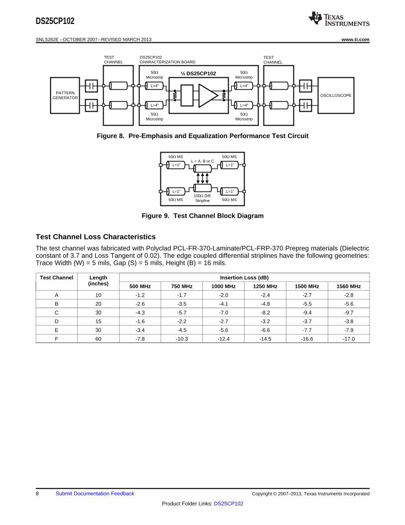
Figure 8. Pre-Emphasis and Equalization Performance Test Circuit
Figure 9. Test Channel Block Diagram
Test Channel Loss Characteristics
The test channel was fabricated with Polyclad PCL-FR-370-Laminate/PCL-FRP-370 Prepreg materials (Dielectricconstant of 3.7 and Loss Tangent of 0.02). The edge coupled differential striplines have the following geometries:Trace Width (W) = 5 mils, Gap (S) = 5 mils, Height (B) = 16 mils.
Test Channel Length Insertion Loss (dB)(inches) 500 MHz 750 MHz 1000 MHz 1250 MHz 1500 MHz 1560 MHz
www.ti.com SNLS262E –OCTOBER 2007–REVISED MARCH 2013
Functional Description
The DS25CP102 is a 3.125 Gbps 2x2 LVDS digital crosspoint switch optimized for high-speed signal routing andswitching over lossy FR-4 printed circuit board backplanes and balanced cables.
Table 1. Switch Configuration Truth Table
SEL1 SEL0 OUT1 OUT0
0 0 IN0 IN0
0 1 IN0 IN1
1 0 IN1 IN0
1 1 IN1 IN1
Table 2. Output Enable Truth Table
EN1 EN0 OUT1 OUT0
0 0 Disabled Disabled
0 1 Disabled Enabled
1 0 Enabled Disabled
1 1 Enabled Enabled
In addition, the DS25CP102 has a pre-emphasis control pin for switching the transmit pre-emphasis to ON andOFF setting and an equalization control pin for switching the receive equalization to ON and OFF setting. Thefollowing are the transmit pre-emphasis and receive equalization truth tables.
Table 3. Transmit Pre-Emphasis Truth Table (1)
OUTPUTS OUT0 and OUT1
CONTROL Pin (PE) State Pre-Emphasis Level
0 OFF
1 ON
(1) Transmit Pre-Emphasis Level Selection
Table 4. Receive Equalization Truth Table (1)
INPUTS IN0 and IN1
CONTROL Pin (EQ) State Equalization Level
0 OFF
1 ON
(1) Receive Equalization Level Selection
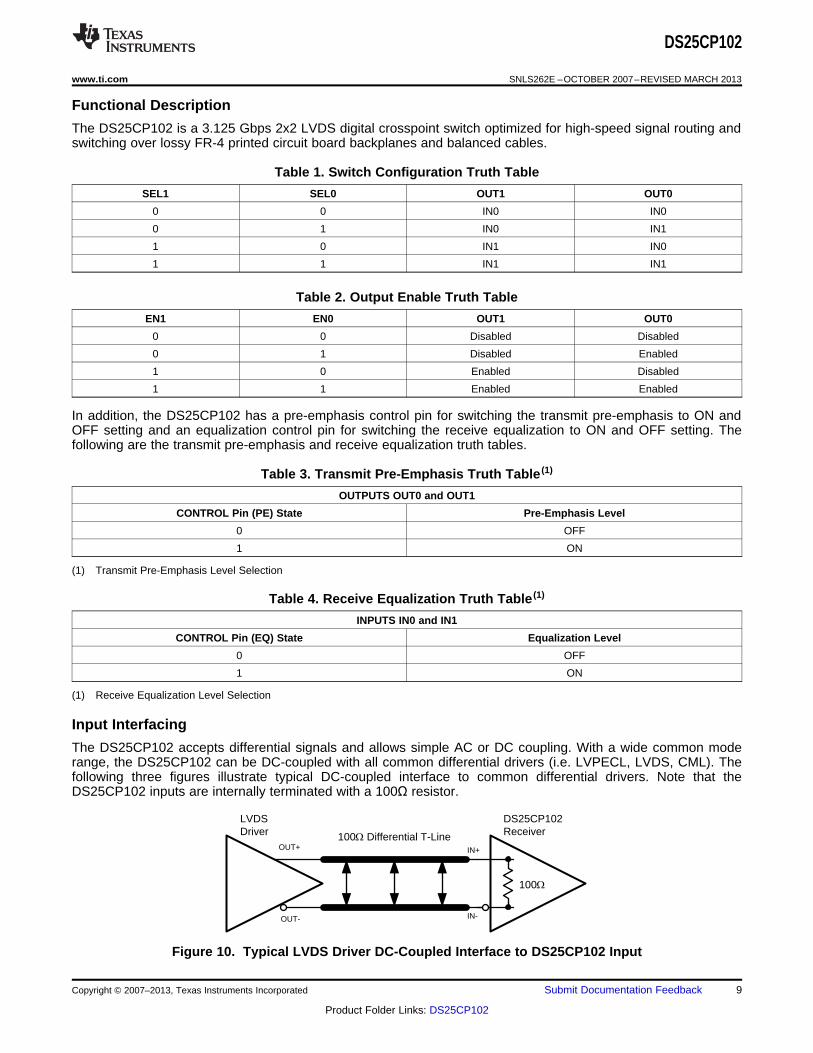
Input Interfacing
The DS25CP102 accepts differential signals and allows simple AC or DC coupling. With a wide common moderange, the DS25CP102 can be DC-coupled with all common differential drivers (i.e. LVPECL, LVDS, CML). Thefollowing three figures illustrate typical DC-coupled interface to common differential drivers. Note that theDS25CP102 inputs are internally terminated with a 100Ω resistor.
Figure 10. Typical LVDS Driver DC-Coupled Interface to DS25CP102 Input
SNLS262E –OCTOBER 2007–REVISED MARCH 2013 www.ti.com
Figure 11. Typical CML Driver DC-Coupled Interface to DS25CP102 Input
Figure 12. Typical LVPECL Driver DC-Coupled Interface to DS25CP102 Input
Output Interfacing
The DS25CP102 outputs signals that are compliant to the LVDS standard. Its outputs can be DC-coupled tomost common differential receivers. The following figure illustrates typical DC-coupled interface to commondifferential receivers and assumes that the receivers have high impedance inputs. While most differentialreceivers have a common mode input range that can accommodate LVDS compliant signals, it is recommendedto check respective receiver's data sheet prior to implementing the suggested interface implementation.
Figure 13. Typical DS25CP102 Output DC-Coupled Interface to an LVDS, CML or LVPECL Receiver
www.ti.com SNLS262E –OCTOBER 2007–REVISED MARCH 2013
Typical Performance Characteristics
Figure 14. Total Jitter as a Function of Data Rate Figure 15. Total Jitter as a Function of Input Common ModeVoltage
Figure 16. Residual Jitter as a Function of Data Rate, FR4 Figure 17. Residual Jitter as a Function of Data Rate, FR4Stripline Length and PE Level Stripline Length and EQ Level
SNLS262E –OCTOBER 2007–REVISED MARCH 2013 www.ti.com
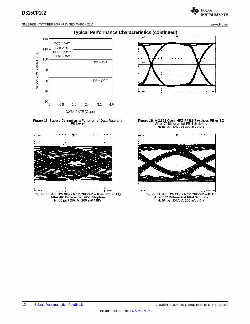
Typical Performance Characteristics (continued)
Figure 18. Supply Current as a Function of Data Rate and Figure 19. A 3.125 Gbps NRZ PRBS-7 without PE or EQPE Level After 2" Differential FR-4 Stripline
H: 50 ps / DIV, V: 100 mV / DIV
Figure 20. A 3.125 Gbps NRZ PRBS-7 without PE or EQ Figure 21. A 3.125 Gbps NRZ PRBS-7 with PEAfter 40" Differential FR-4 Stripline After 40" Differential FR-4 Stripline
H: 50 ps / DIV, V: 100 mV / DIV H: 50 ps / DIV, V: 100 mV / DIV
www.ti.com SNLS262E –OCTOBER 2007–REVISED MARCH 2013
REVISION HISTORY
Changes from Revision D (March 2013) to Revision E Page
• Changed layout of National Data Sheet to TI format .......................................................................................................... 12
DS25CP102TSQ/NOPB ACTIVE WQFN RGH 16 1000 Green (RoHS& no Sb/Br)
CU SN Level-1-260C-UNLIM -40 to 85 2C102SQ
(1) The marketing status values are defined as follows:ACTIVE: Product device recommended for new designs.LIFEBUY: TI has announced that the device will be discontinued, and a lifetime-buy period is in effect.NRND: Not recommended for new designs. Device is in production to support existing customers, but TI does not recommend using this part in a new design.PREVIEW: Device has been announced but is not in production. Samples may or may not be available.OBSOLETE: TI has discontinued the production of the device.
(2) Eco Plan - The planned eco-friendly classification: Pb-Free (RoHS), Pb-Free (RoHS Exempt), or Green (RoHS & no Sb/Br) - please check http://www.ti.com/productcontent for the latest availabilityinformation and additional product content details.TBD: The Pb-Free/Green conversion plan has not been defined.Pb-Free (RoHS): TI's terms "Lead-Free" or "Pb-Free" mean semiconductor products that are compatible with the current RoHS requirements for all 6 substances, including the requirement thatlead not exceed 0.1% by weight in homogeneous materials. Where designed to be soldered at high temperatures, TI Pb-Free products are suitable for use in specified lead-free processes.Pb-Free (RoHS Exempt): This component has a RoHS exemption for either 1) lead-based flip-chip solder bumps used between the die and package, or 2) lead-based die adhesive used betweenthe die and leadframe. The component is otherwise considered Pb-Free (RoHS compatible) as defined above.Green (RoHS & no Sb/Br): TI defines "Green" to mean Pb-Free (RoHS compatible), and free of Bromine (Br) and Antimony (Sb) based flame retardants (Br or Sb do not exceed 0.1% by weightin homogeneous material)
(3) MSL, Peak Temp. - The Moisture Sensitivity Level rating according to the JEDEC industry standard classifications, and peak solder temperature.
(4) There may be additional marking, which relates to the logo, the lot trace code information, or the environmental category on the device.
(5) Multiple Device Markings will be inside parentheses. Only one Device Marking contained in parentheses and separated by a "~" will appear on a device. If a line is indented then it is a continuationof the previous line and the two combined represent the entire Device Marking for that device.
(6) Lead/Ball Finish - Orderable Devices may have multiple material finish options. Finish options are separated by a vertical ruled line. Lead/Ball Finish values may wrap to two lines if the finishvalue exceeds the maximum column width.
Important Information and Disclaimer:The information provided on this page represents TI's knowledge and belief as of the date that it is provided. TI bases its knowledge and belief on informationprovided by third parties, and makes no representation or warranty as to the accuracy of such information. Efforts are underway to better integrate information from third parties. TI has taken andcontinues to take reasonable steps to provide representative and accurate information but may not have conducted destructive testing or chemical analysis on incoming materials and chemicals.TI and TI suppliers consider certain information to be proprietary, and thus CAS numbers and other limited information may not be available for release.
In no event shall TI's liability arising out of such information exceed the total purchase price of the TI part(s) at issue in this document sold by TI to Customer on an annual basis.
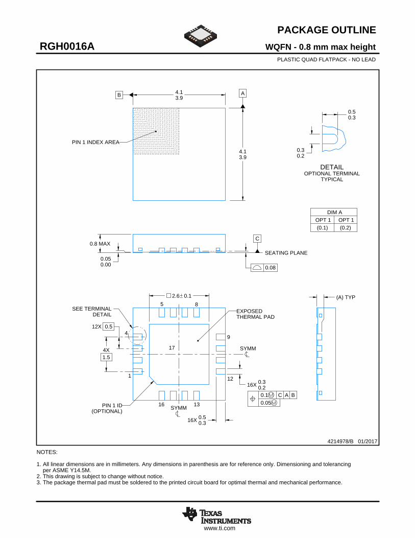
WQFN - 0.8 mm max heightRGH0016APLASTIC QUAD FLATPACK - NO LEAD
4214978/B 01/2017
DIM A OPT 1 OPT 1(0.1) (0.2)
PIN 1 INDEX AREA
0.08
SEATING PLANE
1
49
12
5 8
16 13(OPTIONAL)
PIN 1 ID
0.1 C A B0.05
EXPOSEDTHERMAL PAD
17 SYMM
SYMM
NOTES: 1. All linear dimensions are in millimeters. Any dimensions in parenthesis are for reference only. Dimensioning and tolerancing per ASME Y14.5M. 2. This drawing is subject to change without notice. 3. The package thermal pad must be soldered to the printed circuit board for optimal thermal and mechanical performance.
SCALE 3.000
DETAILOPTIONAL TERMINAL
TYPICAL
www.ti.com
EXAMPLE BOARD LAYOUT
0.07 MINALL AROUND
0.07 MAXALL AROUND
16X (0.25)
16X (0.6)
( 0.2) TYPVIA
12X (0.5)
(3.8)
(3.8)
(1)
( 2.6)
(R0.05)TYP
(1)
WQFN - 0.8 mm max heightRGH0016APLASTIC QUAD FLATPACK - NO LEAD
4214978/B 01/2017
SYMM
1
4
5 8
9
12
1316
SYMM
LAND PATTERN EXAMPLEEXPOSED METAL SHOWN
SCALE:15X
17
NOTES: (continued) 4. This package is designed to be soldered to a thermal pad on the board. For more information, see Texas Instruments literature number SLUA271 (www.ti.com/lit/slua271).5. Vias are optional depending on application, refer to device data sheet. If any vias are implemented, refer to their locations shown on this view. It is recommended that vias under paste be filled, plugged or tented.
SOLDER MASKOPENING
METAL UNDERSOLDER MASK
SOLDER MASKDEFINED
EXPOSED METALMETAL
SOLDER MASKOPENING
SOLDER MASK DETAILS
NON SOLDER MASKDEFINED
(PREFERRED)
EXPOSED METAL
www.ti.com
EXAMPLE STENCIL DESIGN
16X (0.6)
16X (0.25)
12X (0.5)
(3.8)
(3.8)
4X ( 1.15)
(0.675)TYP
(0.675) TYP
(R0.05)TYP
WQFN - 0.8 mm max heightRGH0016APLASTIC QUAD FLATPACK - NO LEAD
4214978/B 01/2017
NOTES: (continued) 6. Laser cutting apertures with trapezoidal walls and rounded corners may offer better paste release. IPC-7525 may have alternate design recommendations.
SYMM
TYPEXPOSED METAL
SOLDER PASTE EXAMPLEBASED ON 0.125 mm THICK STENCIL
EXPOSED PAD 17
78% PRINTED SOLDER COVERAGE BY AREA UNDER PACKAGESCALE:20X
SYMM
1
4
5 8
9
12
1316
17
IMPORTANT NOTICE
Texas Instruments Incorporated (TI) reserves the right to make corrections, enhancements, improvements and other changes to itssemiconductor products and services per JESD46, latest issue, and to discontinue any product or service per JESD48, latest issue. Buyersshould obtain the latest relevant information before placing orders and should verify that such information is current and complete.TI’s published terms of sale for semiconductor products (http://www.ti.com/sc/docs/stdterms.htm) apply to the sale of packaged integratedcircuit products that TI has qualified and released to market. Additional terms may apply to the use or sale of other types of TI products andservices.Reproduction of significant portions of TI information in TI data sheets is permissible only if reproduction is without alteration and isaccompanied by all associated warranties, conditions, limitations, and notices. TI is not responsible or liable for such reproduceddocumentation. Information of third parties may be subject to additional restrictions. Resale of TI products or services with statementsdifferent from or beyond the parameters stated by TI for that product or service voids all express and any implied warranties for theassociated TI product or service and is an unfair and deceptive business practice. TI is not responsible or liable for any such statements.Buyers and others who are developing systems that incorporate TI products (collectively, “Designers”) understand and agree that Designersremain responsible for using their independent analysis, evaluation and judgment in designing their applications and that Designers havefull and exclusive responsibility to assure the safety of Designers' applications and compliance of their applications (and of all TI productsused in or for Designers’ applications) with all applicable regulations, laws and other applicable requirements. Designer represents that, withrespect to their applications, Designer has all the necessary expertise to create and implement safeguards that (1) anticipate dangerousconsequences of failures, (2) monitor failures and their consequences, and (3) lessen the likelihood of failures that might cause harm andtake appropriate actions. Designer agrees that prior to using or distributing any applications that include TI products, Designer willthoroughly test such applications and the functionality of such TI products as used in such applications.TI’s provision of technical, application or other design advice, quality characterization, reliability data or other services or information,including, but not limited to, reference designs and materials relating to evaluation modules, (collectively, “TI Resources”) are intended toassist designers who are developing applications that incorporate TI products; by downloading, accessing or using TI Resources in anyway, Designer (individually or, if Designer is acting on behalf of a company, Designer’s company) agrees to use any particular TI Resourcesolely for this purpose and subject to the terms of this Notice.TI’s provision of TI Resources does not expand or otherwise alter TI’s applicable published warranties or warranty disclaimers for TIproducts, and no additional obligations or liabilities arise from TI providing such TI Resources. TI reserves the right to make corrections,enhancements, improvements and other changes to its TI Resources. TI has not conducted any testing other than that specificallydescribed in the published documentation for a particular TI Resource.Designer is authorized to use, copy and modify any individual TI Resource only in connection with the development of applications thatinclude the TI product(s) identified in such TI Resource. NO OTHER LICENSE, EXPRESS OR IMPLIED, BY ESTOPPEL OR OTHERWISETO ANY OTHER TI INTELLECTUAL PROPERTY RIGHT, AND NO LICENSE TO ANY TECHNOLOGY OR INTELLECTUAL PROPERTYRIGHT OF TI OR ANY THIRD PARTY IS GRANTED HEREIN, including but not limited to any patent right, copyright, mask work right, orother intellectual property right relating to any combination, machine, or process in which TI products or services are used. Informationregarding or referencing third-party products or services does not constitute a license to use such products or services, or a warranty orendorsement thereof. Use of TI Resources may require a license from a third party under the patents or other intellectual property of thethird party, or a license from TI under the patents or other intellectual property of TI.TI RESOURCES ARE PROVIDED “AS IS” AND WITH ALL FAULTS. TI DISCLAIMS ALL OTHER WARRANTIES ORREPRESENTATIONS, EXPRESS OR IMPLIED, REGARDING RESOURCES OR USE THEREOF, INCLUDING BUT NOT LIMITED TOACCURACY OR COMPLETENESS, TITLE, ANY EPIDEMIC FAILURE WARRANTY AND ANY IMPLIED WARRANTIES OFMERCHANTABILITY, FITNESS FOR A PARTICULAR PURPOSE, AND NON-INFRINGEMENT OF ANY THIRD PARTY INTELLECTUALPROPERTY RIGHTS. TI SHALL NOT BE LIABLE FOR AND SHALL NOT DEFEND OR INDEMNIFY DESIGNER AGAINST ANY CLAIM,INCLUDING BUT NOT LIMITED TO ANY INFRINGEMENT CLAIM THAT RELATES TO OR IS BASED ON ANY COMBINATION OFPRODUCTS EVEN IF DESCRIBED IN TI RESOURCES OR OTHERWISE. IN NO EVENT SHALL TI BE LIABLE FOR ANY ACTUAL,DIRECT, SPECIAL, COLLATERAL, INDIRECT, PUNITIVE, INCIDENTAL, CONSEQUENTIAL OR EXEMPLARY DAMAGES INCONNECTION WITH OR ARISING OUT OF TI RESOURCES OR USE THEREOF, AND REGARDLESS OF WHETHER TI HAS BEENADVISED OF THE POSSIBILITY OF SUCH DAMAGES.Unless TI has explicitly designated an individual product as meeting the requirements of a particular industry standard (e.g., ISO/TS 16949and ISO 26262), TI is not responsible for any failure to meet such industry standard requirements.Where TI specifically promotes products as facilitating functional safety or as compliant with industry functional safety standards, suchproducts are intended to help enable customers to design and create their own applications that meet applicable functional safety standardsand requirements. Using products in an application does not by itself establish any safety features in the application. Designers mustensure compliance with safety-related requirements and standards applicable to their applications. Designer may not use any TI products inlife-critical medical equipment unless authorized officers of the parties have executed a special contract specifically governing such use.Life-critical medical equipment is medical equipment where failure of such equipment would cause serious bodily injury or death (e.g., lifesupport, pacemakers, defibrillators, heart pumps, neurostimulators, and implantables). Such equipment includes, without limitation, allmedical devices identified by the U.S. Food and Drug Administration as Class III devices and equivalent classifications outside the U.S.TI may expressly designate certain products as completing a particular qualification (e.g., Q100, Military Grade, or Enhanced Product).Designers agree that it has the necessary expertise to select the product with the appropriate qualification designation for their applicationsand that proper product selection is at Designers’ own risk. Designers are solely responsible for compliance with all legal and regulatoryrequirements in connection with such selection.Designer will fully indemnify TI and its representatives against any damages, costs, losses, and/or liabilities arising out of Designer’s non-compliance with the terms and provisions of this Notice.