12
DS25CP104A,LMH0302,LMH0340,LMH0341, LMH0344,LMH0356 Literature Number: SNOA827

DS25CP104A,LMH0302,LMH0340,LMH0341,LMH0344,LMH0356
Literature Number: SNOA827

LVDS2000 1 of 10 Rev 1.3 © 2008, National Semiconductor Corp.
Evaluating the performance of DS25CP104 in 3G SDI router applications
National Semiconductor Lab Report Keith Spaulding August 20, 2008
Purpose: The DS25CP104 is an excellent candidate for crosspoint switch functions in 3G SDI router applications. To ensure the DS25CP104 will function optimally in these applications the device was tested using pathological video patterns in a full 3G SDI router configuration. Jitter measurements and eye diagrams were taken with various cable lengths before the cable equalizer and with FR4 before and after the DS25CP104. Procedure: Data was taken in numerous configurations. For each setup a block diagram is shown with the jitter data and eye diagram that follows. The following equipment was used in these setups:
• Smart SerDes (LMH0340/LMH0341) EVK - Contains ALP100 with Xilinx Spartan-3E FPGA, LMH0340 EVK (serializer), LMH0341 (deserializer); ALP GUI provides a serial data signal (Matrix Pathological patterns, 3G S274 M 1080 p50) for jitter and eye diagrams and PRBS 11 for jitter and BERT (5.0V)
• SD344EVK: LMH0344 3 Gbps SDI adaptive cable equalizer evaluation kit • SD302EVK: LMH0302 3 Gbps SDI cable driver evaluation kit • SD356EVK: LMH0356 3 Gbps SDI reclocker evaluation kit
• DS25CP104EVK – 3.125 Gbps 4x4 LVDS Crosspoint Switch with Transmit Pre
Emphasis and Receive Equalization (3.3V) • Belden 1694A Cable • TDS6154C (Digital Storage Oscilloscope) with jitter measurement provided from
TDSJIT3 software module. For the 75 ohm input, a 75 ohm BNC adaptor is plugged into the scope; for the 50 ohm input, a 50 ohm SMA adaptor is used.
Coupling arrangements: LMH0340 op/LMH0344 ip – AC coupled, single ended 75 ohm LMH0344 op/DS25CP104 ip – DC coupled, differential 50 ohm DS25CP104 op/LMH0356 op – DC coupled, differential 50 ohm LMH0356 op/LMH0302 ip – AC coupled, differential 50 ohm LMH0302 op/ Scope ip – AC coupled, single ended 75 ohm BERT testing was performed feeding back the output to the internal BERT engine FPGA and ALP software; for each test, 100k bits was transferred using a PRBS 9 pattern.
Figure 1: Final setup

LVDS2000 2 of 10 Rev 1.3 © 2008, National Semiconductor Corp.
Setup/ Results: Jitter and eye diagram data was taken at each step, to show the amount each steps adds to the total jitter of the system. For reference for f = 2.97Gbps, 1 UI = 336 ps
1. Setup 1 : Source (ALP Smart SerDes) with adaptive equalizer (LMH0344)
Figure 2.1 - Block diagram Setup 1
Figure 2.2 – Eye Diagram of Setup 1
Video source pattern Rj (ps) Dj (ps) Tj (ps) Matrix Pathological 3.5 24.1 64.7
Table 1 – Jitter results of Setup 1
BERT: 0 errors for 100k bits sent

LVDS2000 3 of 10 Rev 1.3 © 2008, National Semiconductor Corp.
2. Setup 2: Source (ALP Smart SerDes) with adaptive equalizer (LMH0344) and crosspoint switch (DS25CP104, no PE, no EQ)
Figure 3.1 - Block diagram Setup 2
Figure 3.2 – Eye Diagram of Setup 2
Video source pattern Rj (ps) Dj (ps) Tj (ps) Matrix Pathological 4.2 28.3 74.8
Table 2 – Jitter results of Setup 2
BERT: 0 errors for 100k bits sent

LVDS2000 4 of 10 Rev 1.3 © 2008, National Semiconductor Corp.
For Setup 2 only, jitter is compared for each crosspoint configuration
Rj (ps) Dj (ps) Tj (ps) IN0 OUT0 3.4 20.8 61.9 IN0 OUT1 3.5 27.6 69.4 IN0 OUT2 3.4 28.7 70.7 IN0 OUT3 3.4 29.5 71.5 IN1 OUT0 3.3 26.5 65.3 IN1 OUT1 3.0 23.0 59.0 IN1 OUT2 3.4 22.9 65.0 IN1 OUT3 3.3 22.9 60.8 IN2 OUT0 3.5 30.0 71.8 IN2 OUT1 3.4 26.7 67.5 IN2 OUT2 3.3 18.7 58.7 IN2 OUT3 3.3 22.1 61.5 IN3 OUT0 3.3 24.4 64.8 IN3 OUT1 3.4 28.6 70.0 IN3 OUT2 3.5 27.3 69.3 IN3 OUT3 3.3 24.0 63.5
Table 2.1 – Comparing jitter results for various DS 25CP104 crosspoint configurations

LVDS2000 5 of 10 Rev 1.3 © 2008, National Semiconductor Corp.
3. Setup 3: Source (ALP Smart SerDes) with adaptive equalizer (LMH0344) and crosspoint switch (DS25CP104, no PE, no EQ) and cable driver (LMH0302).
Figure 4.1 - Block diagram Setup 3
Figure 4.2 – Eye Diagram of Setup 3
Video source pattern Rj (ps) Dj (ps) Tj (ps) Matrix Pathological 5.1 36.9 96.3
PRBS11 5.7 31.2 101.5
Table 3 – Jitter results of Setup 3
BERT: 0 errors for 100k bits sent
LVDS2000 6 of 10 Rev 1.3 © 2008, National Semiconductor Corp.
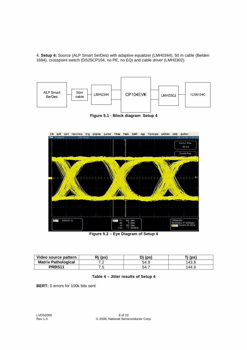
4. Setup 4: Source (ALP Smart SerDes) with adaptive equalizer (LMH0344), 50 m cable (Belden 1694), crosspoint switch (DS25CP104, no PE, no EQ) and cable driver (LMH0302).
Figure 5.1 - Block diagram Setup 4
Figure 5.2 – Eye Diagram of Setup 4
Video source pattern Rj (ps) Dj (ps) Tj (ps) Matrix Pathological 7.2 54.9 143.8
PRBS11 7.5 54.7 144.9
Table 4 – Jitter results of Setup 4
BERT: 0 errors for 100k bits sent

LVDS2000 7 of 10 Rev 1.3 © 2008, National Semiconductor Corp.
5. Setup 5: Source (ALP Smart SerDes) with adaptive equalizer (LMH0344), 50 m cable (Belden 1694), 15 “ FR4 before and after crosspoint switch (DS25CP104, PE - Hi, EQ - H) and cable driver (LMH0302).
Figure 6.1 - Block diagram Setup 5
Figure 6.2 – Eye Diagram of Setup 5
Video source pattern Rj (ps) Dj (ps) Tj (ps) Matrix Pathological 6.6 63.8 140.6
PRBS11 6.9 57.1 141
Table 5 – Jitter results of Setup 5
BERT: 0 errors for 100k bits sent

LVDS2000 8 of 10 Rev 1.3 © 2008, National Semiconductor Corp.
6. Setup 6: Source (ALP Smart SerDes) with adaptive equalizer (LMH0344), 100 m cable (Belden 1694), 15 “ FR4 before and after crosspoint switch (DS25CP104, PE - Hi, EQ - H) and cable driver (LMH0302).
Figure 7.1 - Block diagram Setup 6
Figure 7.2 – Eye Diagram of Setup 6
Video source pattern Rj (ps) Dj (ps) Tj (ps) Matrix Pathological 8.4 70.9 169.6
PRBS11 9.0 63.4 174.2
Table 6 – Jitter results of Setup 6
BERT: 0 errors for 100k bits sent (with PE and EQ Hi), 8.5 x 10⁻⁹ BER (PE and EQ off)

LVDS2000 9 of 10 Rev 1.3 © 2008, National Semiconductor Corp.
Setup 7: Source (ALP Smart SerDes) with adaptive equalizer (LMH0344), 100 m cable (Belden 1694), 15 “ FR4 before and after crosspoint switch (DS25CP104, PE - Hi, EQ - H), reclocker (LMH0356) and cable driver (LMH0302).
Figure 8.1 - Block diagram Setup 7
Figure 8.2 – Eye Diagram of Setup 7
Video source pattern Rj (ps) Dj (ps) Tj (ps) Matrix Pathological 2.23 21.45 47.0
PRBS11 4.3 23.9 74.6
Table 7 – Jitter results of Setup 7
BERT: 0 errors for 100k bits sent (with PE and EQ Hi)

LVDS2000 10 of 10 Rev 1.3 © 2008, National Semiconductor Corp.
Cascading the DS25CP104 If a larger crosspoint switch is desired, cascading DS25CP104s can be effective; data was taken cascading three DS25CP104 channels (Setup 8): PE, EQ off Channels cascaded on one EVK board
Figure 9.1 - Block diagram Setup 8
Test Point Rj (ps) Dj (ps) Tj(ps)
A 3.5 24.1 64.7 B 4.2 28.3 74.8 C 4.5 37.7 88.8 D 5.6 39.5 103.9
Table 8 – Jitter results at each step
Comments Considering the above data, the DS25CP104, with full signal conditioning, is well suited for small crosspoint switch requirements or cascaded for larger crosspoint switch configurations in 3G SDI applications. National's ALP platform has a higher noise floor compared to dedicated pattern generators making it a more realistic source for video application testing purposes. Table 2.1 shows that using pathological patterns, the DS25CP104 outputs, with any crosspoint configuration, will not vary more than 14ps (Tj) and 10ps (Dj); a condition that is within its specification for jitter output variation. Looking at Setup 4 and Setup 5, you see that the signal conditioning of the DS25CP104 completely compensates for 15in. of FR4 before and after the device; both yield a result of about 140ps. Also there were no errors on the BERT. Even though 140ps is 0.4UI, there are not errors and it may fit within the jitter budget of the system as a cost effective solution; if the jitter is two high then the reclocker can be used (decreasing total jitter to 40ps).

IMPORTANT NOTICE
Texas Instruments Incorporated and its subsidiaries (TI) reserve the right to make corrections, modifications, enhancements, improvements,and other changes to its products and services at any time and to discontinue any product or service without notice. Customers shouldobtain the latest relevant information before placing orders and should verify that such information is current and complete. All products aresold subject to TI’s terms and conditions of sale supplied at the time of order acknowledgment.
TI warrants performance of its hardware products to the specifications applicable at the time of sale in accordance with TI’s standardwarranty. Testing and other quality control techniques are used to the extent TI deems necessary to support this warranty. Except wheremandated by government requirements, testing of all parameters of each product is not necessarily performed.
TI assumes no liability for applications assistance or customer product design. Customers are responsible for their products andapplications using TI components. To minimize the risks associated with customer products and applications, customers should provideadequate design and operating safeguards.
TI does not warrant or represent that any license, either express or implied, is granted under any TI patent right, copyright, mask work right,or other TI intellectual property right relating to any combination, machine, or process in which TI products or services are used. Informationpublished by TI regarding third-party products or services does not constitute a license from TI to use such products or services or awarranty or endorsement thereof. Use of such information may require a license from a third party under the patents or other intellectualproperty of the third party, or a license from TI under the patents or other intellectual property of TI.
Reproduction of TI information in TI data books or data sheets is permissible only if reproduction is without alteration and is accompaniedby all associated warranties, conditions, limitations, and notices. Reproduction of this information with alteration is an unfair and deceptivebusiness practice. TI is not responsible or liable for such altered documentation. Information of third parties may be subject to additionalrestrictions.
Resale of TI products or services with statements different from or beyond the parameters stated by TI for that product or service voids allexpress and any implied warranties for the associated TI product or service and is an unfair and deceptive business practice. TI is notresponsible or liable for any such statements.
TI products are not authorized for use in safety-critical applications (such as life support) where a failure of the TI product would reasonablybe expected to cause severe personal injury or death, unless officers of the parties have executed an agreement specifically governingsuch use. Buyers represent that they have all necessary expertise in the safety and regulatory ramifications of their applications, andacknowledge and agree that they are solely responsible for all legal, regulatory and safety-related requirements concerning their productsand any use of TI products in such safety-critical applications, notwithstanding any applications-related information or support that may beprovided by TI. Further, Buyers must fully indemnify TI and its representatives against any damages arising out of the use of TI products insuch safety-critical applications.
TI products are neither designed nor intended for use in military/aerospace applications or environments unless the TI products arespecifically designated by TI as military-grade or "enhanced plastic." Only products designated by TI as military-grade meet militaryspecifications. Buyers acknowledge and agree that any such use of TI products which TI has not designated as military-grade is solely atthe Buyer's risk, and that they are solely responsible for compliance with all legal and regulatory requirements in connection with such use.
TI products are neither designed nor intended for use in automotive applications or environments unless the specific TI products aredesignated by TI as compliant with ISO/TS 16949 requirements. Buyers acknowledge and agree that, if they use any non-designatedproducts in automotive applications, TI will not be responsible for any failure to meet such requirements.
Following are URLs where you can obtain information on other Texas Instruments products and application solutions:
Products Applications
Audio www.ti.com/audio Communications and Telecom www.ti.com/communications
Amplifiers amplifier.ti.com Computers and Peripherals www.ti.com/computers
Data Converters dataconverter.ti.com Consumer Electronics www.ti.com/consumer-apps
DLP® Products www.dlp.com Energy and Lighting www.ti.com/energy
DSP dsp.ti.com Industrial www.ti.com/industrial
Clocks and Timers www.ti.com/clocks Medical www.ti.com/medical
Interface interface.ti.com Security www.ti.com/security
Logic logic.ti.com Space, Avionics and Defense www.ti.com/space-avionics-defense
Power Mgmt power.ti.com Transportation and Automotive www.ti.com/automotive
Microcontrollers microcontroller.ti.com Video and Imaging www.ti.com/video
RFID www.ti-rfid.com
OMAP Mobile Processors www.ti.com/omap
Wireless Connectivity www.ti.com/wirelessconnectivity
TI E2E Community Home Page e2e.ti.com
Mailing Address: Texas Instruments, Post Office Box 655303, Dallas, Texas 75265Copyright © 2011, Texas Instruments Incorporated


