Product Folder Sample & Buy Technical Documents Tools & Software Support & Community DS26C31M, DS26C31T SNLS375C – JUNE 1998 – REVISED JANUARY 2015 DS26C31x CMOS Quad Tri-State Differential Line Driver 1 Features 3 Description The DS26C31 device is a quad differential line driver 1• TTL Input Compatible designed for digital data transmission over balanced • Typical Propagation Delays: 6 ns lines. The DS26C31T meets all the requirements of • Typical Output Skew: 0.5 ns EIA standard RS-422 while retaining the low power characteristics of CMOS. The DS26C31M is • Outputs Will Not Load Line When V CC =0V compatible with EIA standard RS-422; however, one • DS26C31T Meets the Requirements of EIA exception in test methodology is taken (2) . This Standard RS-422 enables the construction of serial and terminal • Operation From Single 5-V Supply interfaces while maintaining minimal power consumption. • Tri-State Outputs for Connection to System Buses • Low Quiescent Current The DS26C31 accepts TTL or CMOS input levels and translates these to RS-422 output levels. This part • Available in Surface Mount uses special output circuitry that enables the drivers • Mil-Std-883C Compliant to power down without loading down the bus. This device has enable and disable circuitry common to all 2 Applications four drivers. The DS26C31 is pin compatible to the Differential Line Driver for RS-422 Applications AM26LS31 and the DS26LS31. All inputs are protected against damage due to electrostatic discharge by diodes to V CC and ground. Device Information (1) PART NUMBER PACKAGE BODY SIZE (NOM) SNLS3759577 9.90 mm × 3.91 mm DS26C31M PDIP (16) 19.304 mm × 6.35 mm SNLS3759577 9.90 mm × 3.91 mm DS26C31T PDIP (16) 19.304 mm × 6.35 mm (1) For all available packages, see the orderable addendum at the end of the datasheet. (2) The DS26C31M (−55°C to 125°C) is tested with V OUT between 6 V and 0 V while RS-422A condition is 6 V and −0.25 V. 4 Device Logic Diagram 1 An IMPORTANT NOTICE at the end of this data sheet addresses availability, warranty, changes, use in safety-critical applications, intellectual property matters and other important disclaimers. PRODUCTION DATA.
Transcript
Product
Folder
Sample &Buy
Technical
Documents
Tools &
Software
Support &Community
DS26C31M, DS26C31TSNLS375C –JUNE 1998–REVISED JANUARY 2015
DS26C31x CMOS Quad Tri-State Differential Line Driver1 Features 3 Description
The DS26C31 device is a quad differential line driver1• TTL Input Compatible
designed for digital data transmission over balanced• Typical Propagation Delays: 6 ns lines. The DS26C31T meets all the requirements of• Typical Output Skew: 0.5 ns EIA standard RS-422 while retaining the low power
characteristics of CMOS. The DS26C31M is• Outputs Will Not Load Line When VCC = 0 Vcompatible with EIA standard RS-422; however, one• DS26C31T Meets the Requirements of EIA exception in test methodology is taken(2). ThisStandard RS-422 enables the construction of serial and terminal
• Operation From Single 5-V Supply interfaces while maintaining minimal powerconsumption.• Tri-State Outputs for Connection to System Buses
• Low Quiescent Current The DS26C31 accepts TTL or CMOS input levels andtranslates these to RS-422 output levels. This part• Available in Surface Mountuses special output circuitry that enables the drivers• Mil-Std-883C Compliant to power down without loading down the bus. Thisdevice has enable and disable circuitry common to all2 Applications four drivers. The DS26C31 is pin compatible to the
Differential Line Driver for RS-422 Applications AM26LS31 and the DS26LS31.
All inputs are protected against damage due toelectrostatic discharge by diodes to VCC and ground.
Device Information(1)
PART NUMBER PACKAGE BODY SIZE (NOM)SNLS3759577 9.90 mm × 3.91 mm
DS26C31MPDIP (16) 19.304 mm × 6.35 mmSNLS3759577 9.90 mm × 3.91 mm
DS26C31TPDIP (16) 19.304 mm × 6.35 mm
(1) For all available packages, see the orderable addendum atthe end of the datasheet.
(2) The DS26C31M (−55°C to 125°C) is tested with VOUTbetween 6 V and 0 V while RS-422A condition is 6 V and−0.25 V.
4 Device Logic Diagram
1
An IMPORTANT NOTICE at the end of this data sheet addresses availability, warranty, changes, use in safety-critical applications,intellectual property matters and other important disclaimers. PRODUCTION DATA.
5 Revision HistoryNOTE: Page numbers for previous revisions may differ from page numbers in the current version.
Changes from Revision B (April 2013) to Revision C Page
• Added Feature Description section, Device Functional Modes, Application and Implementation section, PowerSupply Recommendations section, Layout section, Device and Documentation Support section, and Mechanical,Packaging, and Orderable Information section ...................................................................................................................... 1
Changes from Revision A (April 2013) to Revision B Page
• Changed layout of National Data Sheet to TI format ............................................................................................................. 9
DS26C31M, DS26C31Twww.ti.com SNLS375C –JUNE 1998–REVISED JANUARY 2015
6 Pin Configuration and Functions
D, NFG PackageNAJ Package16 Pins
20 PinsTop ViewTop View
Pin FunctionsPIN
I/O DESCRIPTIONNAME NO. (1)
DIFFERENTIAL SIGNALING I/OCHANNEL A 3, 2 O Channel A inverting and non-inverting differential driver outputsOUTPUTS (–, +)CHANNEL B 5, 6 O Channel B inverting and non-inverting differential driver outputsOUTPUTS (–, +)CHANNEL C 11, 10 O Channel C inverting and non-inverting differential driver outputsOUTPUTS (–, +)CHANNEL D 13, 14 O Channel D inverting and non-inverting differential driver outputsOUTPUTS (–, +)INPUT A 1 I TTL/CMOS compatible input for channel AINPUT B 7 I TTL/CMOS compatible input for channel BINPUT C 9 I TTL/CMOS compatible input for channel CINPUT D 15 I TTL/CMOS compatible input for channel DCONTROL PINSENABLE 4 I Logic-high ENABLE ControlENABLE 12 I Logic-low ENABLE ControlPOWERGND 8 — GND PinVCC 16 — Supply pin, provide 5 V supply
(1) Pin numbers correspond to PDIP and SOIC packages.
DS26C31M, DS26C31TSNLS375C –JUNE 1998–REVISED JANUARY 2015 www.ti.com
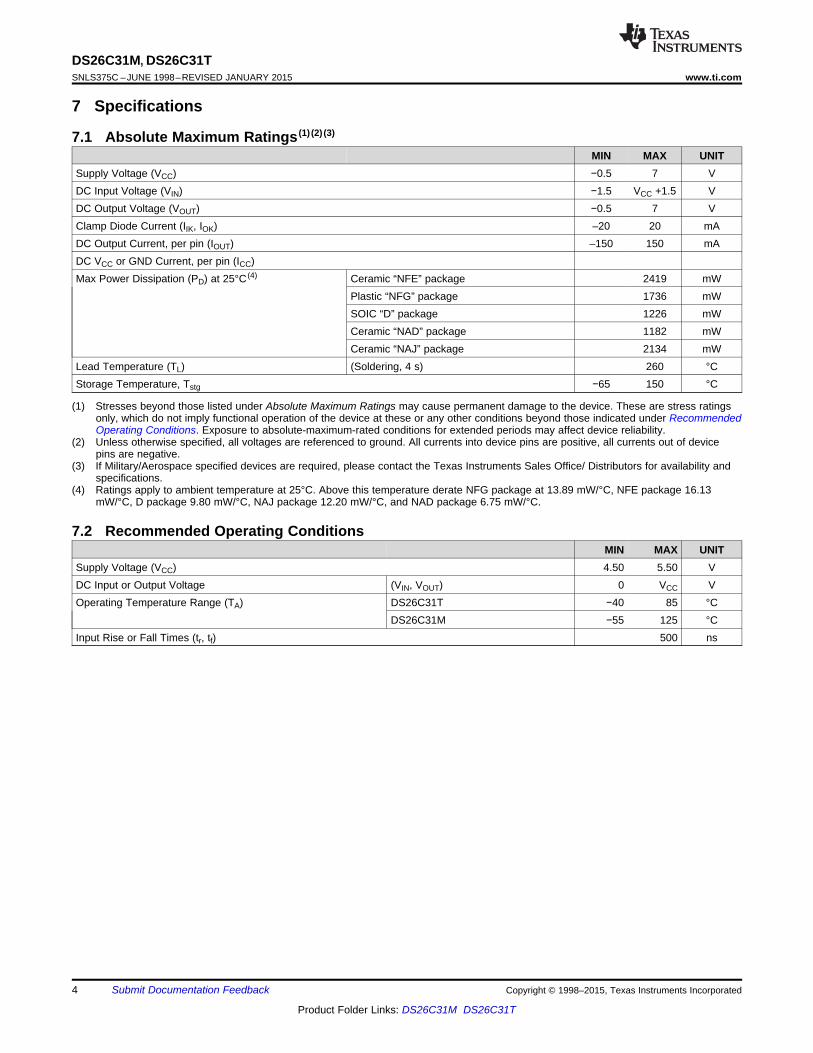
7 Specifications
7.1 Absolute Maximum Ratings (1) (2) (3)
MIN MAX UNITSupply Voltage (VCC) −0.5 7 VDC Input Voltage (VIN) −1.5 VCC +1.5 VDC Output Voltage (VOUT) −0.5 7 VClamp Diode Current (IIK, IOK) –20 20 mADC Output Current, per pin (IOUT) –150 150 mADC VCC or GND Current, per pin (ICC)Max Power Dissipation (PD) at 25°C (4) Ceramic “NFE” package 2419 mW
Lead Temperature (TL) (Soldering, 4 s) 260 °CStorage Temperature, Tstg −65 150 °C
(1) Stresses beyond those listed under Absolute Maximum Ratings may cause permanent damage to the device. These are stress ratingsonly, which do not imply functional operation of the device at these or any other conditions beyond those indicated under RecommendedOperating Conditions. Exposure to absolute-maximum-rated conditions for extended periods may affect device reliability.
(2) Unless otherwise specified, all voltages are referenced to ground. All currents into device pins are positive, all currents out of devicepins are negative.
(3) If Military/Aerospace specified devices are required, please contact the Texas Instruments Sales Office/ Distributors for availability andspecifications.
(4) Ratings apply to ambient temperature at 25°C. Above this temperature derate NFG package at 13.89 mW/°C, NFE package 16.13mW/°C, D package 9.80 mW/°C, NAJ package 12.20 mW/°C, and NAD package 6.75 mW/°C.
7.2 Recommended Operating ConditionsMIN MAX UNIT
Supply Voltage (VCC) 4.50 5.50 VDC Input or Output Voltage (VIN, VOUT) 0 VCC VOperating Temperature Range (TA) DS26C31T −40 85 °C
DS26C31M −55 125 °CInput Rise or Fall Times (tr, tf) 500 ns
DS26C31M, DS26C31Twww.ti.com SNLS375C –JUNE 1998–REVISED JANUARY 2015
7.3 DC Electrical CharacteristicsVCC = 5 V ± 10% (unless otherwise specified) (1)
PARAMETER TEST CONDITIONS MIN TYP MAX UNITVIH High Level Input Voltage 2.0 VVIL Low Level Input Voltage 0.8 VVOH High Level Output Voltage VIN = VIH or VIL, 2.5 3.4 V
IOUT = −20 mAVOL Low Level Output Voltage VIN = VIH or VIL, 0.3 0.5 V
IOUT = 20 mAVT Differential Output Voltage RL = 100 Ω 2.0 3.1 V
VOS Common Mode Output Voltage RL = 100 Ω 1.8 3.0 VSee (2)
|VOS − VOS | Difference In Common Mode RL = 100 Ω 0.4 VOutput See (2)
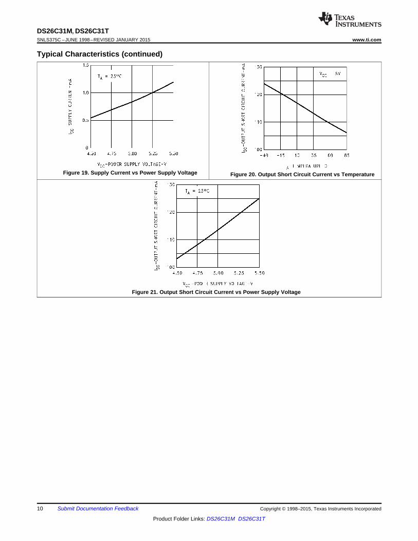
IIN Input Current VIN = VCC, GND, VIH, or VIL ±1.0 μAICC Quiescent Supply Current (3) DS26C31T VIN = VCC or GND 200 500 μA
IOUT = 0 μA VIN = 2.4 V or 0.5 V (3) 0.8 2.0 mADS26C31M VIN = VCC or GND 200 500 μAIOUT = 0 μA VIN = 2.4 V or 0.5 V (3) 0.8 2.1 mA
IOZ TRI-STATE Output Leakage VOUT = VCC or GNDCurrent ENABLE = VIL ±0.5 ±5.0 μA
ENABLE = VIH
ISC Output Short Circuit Current VIN = VCC or GND (2) (4) −30 −150 mAIOFF Output Leakage Current Power DS26C31T VOUT = 6 V 100 μA
Off (2)VCC = 0 V VOUT = −0.25 V −100 μADS26C31M VOUT = 6 V 100 μAVCC = 0 V VOUT = 0 V (5) −100 μA
(1) Unless otherwise specified, min/max limits apply across the recommended operating temperature range. All typicals are given for VCC =5 V and TA = 25°C.
(2) See EIA Specification RS-422 for exact test conditions.(3) Measured per input. All other inputs at VCC or GND.(4) This is the current sourced when a high output is shorted to ground. Only one output at a time should be shorted.(5) The DS26C31M (−55°C to +125°C) is tested with VOUT between +6 V and 0 V while RS-422A condition is +6 V and −0.25 V.
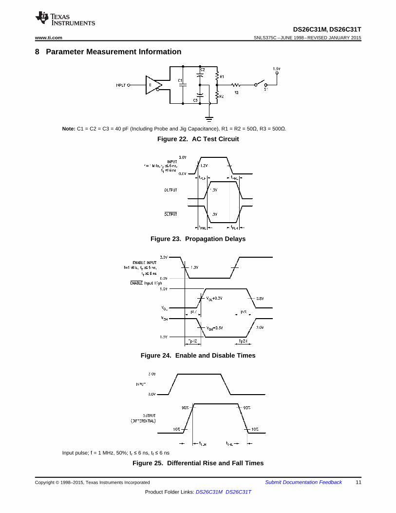
DS26C31T DS26C31MPARAMETER TEST CONDITIONS MIN TYP UNIT
MAX MAXtPLH, tPHL Propagation Delays Input to Output S1 Open 2 6 11 14 nsSkew (2) S1 Open 0.5 2.0 3.0 nstTLH, tTHL Differential Output Rise And Fall S1 Open 6 10 14 ns
TimestPZH Output Enable Time S1 Closed 11 19 22 nstPZL Output Enable Time S1 Closed 13 21 28 nstPHZ Output Disable Time (3) S1 Closed 5 9 12 nstPLZ Output Disable Time (3) S1 Closed 7 11 14 nsCPD Power Dissipation Capacitance (4) 50 pFCIN Input Capacitance 6 pF
(1) Unless otherwise specified, min/max limits apply across the recommended operating temperature range. All typicals are given for VCC =5 V and TA = 25°C.
(2) Skew is defined as the difference in propagation delays between complementary outputs at the 50% point.(3) Output disable time is the delay from ENABLE or ENABLE being switched to the output transistors turning off. The actual disable times
are less than indicated due to the delay added by the RC time constant of the load.(4) CPD determines the no load dynamic power consumption, PD = CPD VCC2 f + ICC VCC, and the no load dynamic current consumption, IS
tTHL, tTLH Differential Output Rise and Fall CL = 30 pFTimes S1 Closed 4 6 ns
S2 ClosedtPLZ Output Disable Time (3) CL = 10 pF
S1 Closed 6 9 15 35 nsS2 Open
tPHZ Output Disable Time (3) CL = 10 pFS1 Open 4 7 15 25 nsS2 Closed
tPZL Output Enable Time CL = 30 pFS1 Closed 14 20 20 30 nsS2 Open
tPZH Output Enable Time CL = 30 pFS1 Open 11 17 20 30 nsS2 Closed
(1) This table is provided for comparison purposes only. The values in this table for the DS26C31 reflect the performance of the device butare not tested or verified.
(2) Skew is defined as the difference in propagation delays between complementary outputs at the 50% point.(3) Output disable time is the delay from ENABLE or ENABLE being switched to the output transistors turning off. The actual disable times
are less than indicated due to the delay added by the RC time constant of the load.
DS26C31M, DS26C31Twww.ti.com SNLS375C –JUNE 1998–REVISED JANUARY 2015
9 Detailed Description
9.1 OverviewThe DS26C31 is a quad differential line driver designed for data transmission over balanced cable or printedcircuit board traces. The DS26C31M supports a temperature range of -55°C to 125°C, while the DS26C31Tsupports a temperature range of -40°C to 85°C.
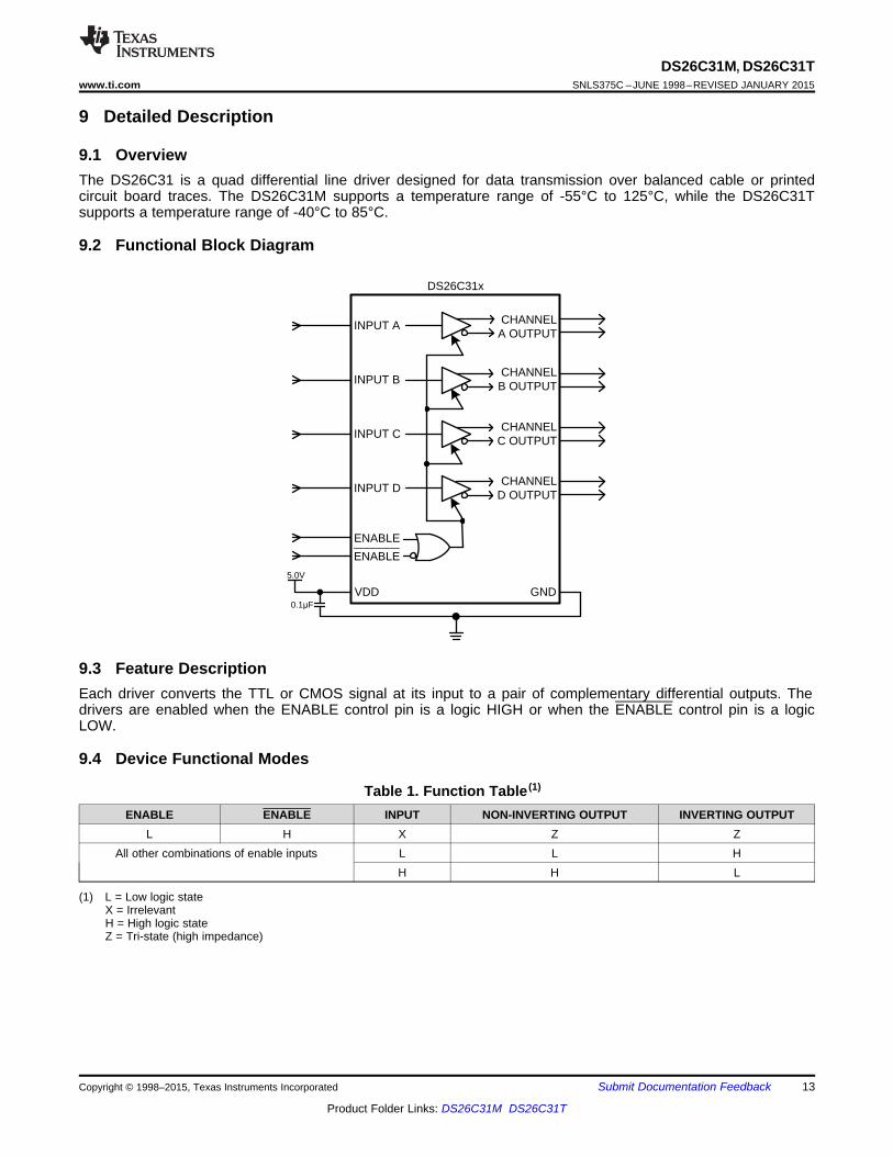
9.2 Functional Block Diagram
9.3 Feature DescriptionEach driver converts the TTL or CMOS signal at its input to a pair of complementary differential outputs. Thedrivers are enabled when the ENABLE control pin is a logic HIGH or when the ENABLE control pin is a logicLOW.
9.4 Device Functional Modes
Table 1. Function Table (1)
ENABLE ENABLE INPUT NON-INVERTING OUTPUT INVERTING OUTPUTL H X Z Z
All other combinations of enable inputs L L HH H L
(1) L = Low logic stateX = IrrelevantH = High logic stateZ = Tri-state (high impedance)
DS26C31M, DS26C31TSNLS375C –JUNE 1998–REVISED JANUARY 2015 www.ti.com
10 Application and Implementation
NOTEInformation in the following applications sections is not part of the TI componentspecification, and TI does not warrant its accuracy or completeness. TI’s customers areresponsible for determining suitability of components for their purposes. Customers shouldvalidate and test their design implementation to confirm system functionality.
10.1 Application InformationThe DS26C31 is a quad differential line driver designed for applications that require long distance digital datatransmission over balanced cables. The DS26C31 can be used in applications that require conversion from TTLor CMOS input levels to differential signal levels, compatible to RS-422. The use of complimentary signaling in abalanced transmission media provides good immunity in the midst of noisy environments or shifts in groundreference potential.
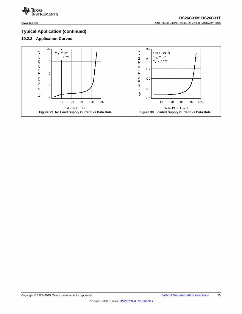
10.2 Typical ApplicationFigure 28 depicts a typical implementation of the DS26C31x device in a RS-422 application.
*RT is optional although highly recommended to reduce reflection.
Figure 28. Two-Wire Balanced System, RS-422
10.2.1 Design Requirements• Apply TTL or LVCMOS signal to driver input lines INPUT A-D.• Transmit complementary outputs at OUTPUT A-D.• Use controlled-impedance transmission lines such as printed circuit board traces, twisted-pair wires or parallel
wire cable.• Place a terminating resistor at the far end of the differential pair.
10.2.2 Detailed Design Procedure• Connect VCC and GND pins to the power and ground planes of the PCB with a 0.1-µF bypass capacitor.• Use TTL/LVCMOS logic levels at INPUT A-D.• Use controlled-impedance transmission media for the differential output signals.• Place an optional terminating resistor at the far-end of the differential pair to avoid reflection.
DS26C31M, DS26C31TSNLS375C –JUNE 1998–REVISED JANUARY 2015 www.ti.com
11 Power Supply RecommendationsIt is recommended that the supply (VCC) and ground (GND) pins be connected to power planes that are placedin the inner layers of the printed circuit board. A 0.1-µF bypass capacitor should be connect to the VCC pin suchthat the capacitor is as close as possible to the device.
12 Layout
12.1 Layout GuidelinesThe output differential signals of the device should be routed on one layer of the board, and clearance should beprovided in order to minimize crosstalk between differential pairs that may be running in parallel over a longdistance. Additionally, the differential pairs should have a controlled impedance with minimum impedancediscontinuities and be terminated at the far-end, near the receiver, with a resistor that is closely matched to thedifferential pair impedance in order to minimize transmission line reflections. The differential pairs should berouted with uniform trace width and spacing to minimize impedance mismatching.
DS26C31M, DS26C31Twww.ti.com SNLS375C –JUNE 1998–REVISED JANUARY 2015
13 Device and Documentation Support
13.1 Related LinksThe table below lists quick access links. Categories include technical documents, support and communityresources, tools and software, and quick access to sample or buy.
Table 2. Related LinksTECHNICAL TOOLS & SUPPORT &PARTS PRODUCT FOLDER SAMPLE & BUY DOCUMENTS SOFTWARE COMMUNITY
DS26C31M Click here Click here Click here Click here Click hereDS26C31T Click here Click here Click here Click here Click here
13.2 TrademarksAll trademarks are the property of their respective owners.
13.3 Electrostatic Discharge CautionThese devices have limited built-in ESD protection. The leads should be shorted together or the device placed in conductive foamduring storage or handling to prevent electrostatic damage to the MOS gates.
13.4 GlossarySLYZ022 — TI Glossary.
This glossary lists and explains terms, acronyms, and definitions.
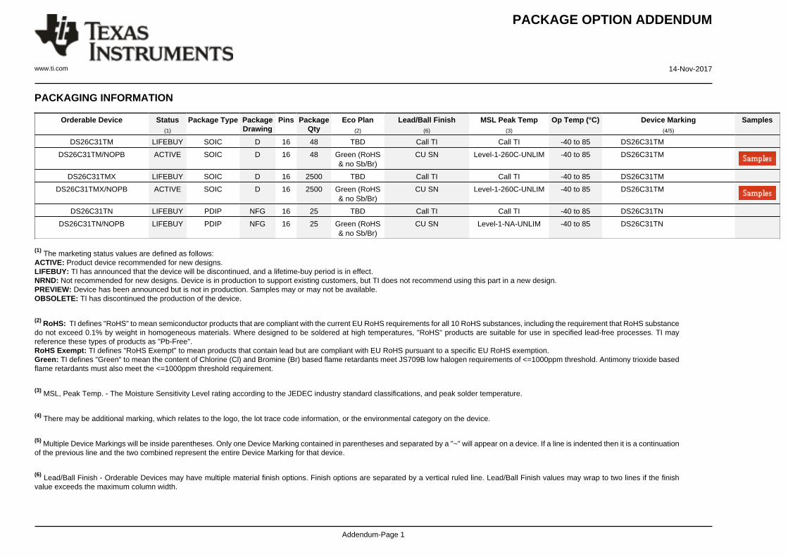
14 Mechanical, Packaging, and Orderable InformationThe following pages include mechanical, packaging, and orderable information. This information is the mostcurrent data available for the designated devices. This data is subject to change without notice and revision ofthis document. For browser-based versions of this data sheet, refer to the left-hand navigation.
DS26C31TM LIFEBUY SOIC D 16 48 TBD Call TI Call TI -40 to 85 DS26C31TM
DS26C31TM/NOPB ACTIVE SOIC D 16 48 Green (RoHS& no Sb/Br)
CU SN Level-1-260C-UNLIM -40 to 85 DS26C31TM
DS26C31TMX LIFEBUY SOIC D 16 2500 TBD Call TI Call TI -40 to 85 DS26C31TM
DS26C31TMX/NOPB ACTIVE SOIC D 16 2500 Green (RoHS& no Sb/Br)
CU SN Level-1-260C-UNLIM -40 to 85 DS26C31TM
DS26C31TN LIFEBUY PDIP NFG 16 25 TBD Call TI Call TI -40 to 85 DS26C31TN
DS26C31TN/NOPB LIFEBUY PDIP NFG 16 25 Green (RoHS& no Sb/Br)
CU SN Level-1-NA-UNLIM -40 to 85 DS26C31TN
(1) The marketing status values are defined as follows:ACTIVE: Product device recommended for new designs.LIFEBUY: TI has announced that the device will be discontinued, and a lifetime-buy period is in effect.NRND: Not recommended for new designs. Device is in production to support existing customers, but TI does not recommend using this part in a new design.PREVIEW: Device has been announced but is not in production. Samples may or may not be available.OBSOLETE: TI has discontinued the production of the device.
(2) RoHS: TI defines "RoHS" to mean semiconductor products that are compliant with the current EU RoHS requirements for all 10 RoHS substances, including the requirement that RoHS substancedo not exceed 0.1% by weight in homogeneous materials. Where designed to be soldered at high temperatures, "RoHS" products are suitable for use in specified lead-free processes. TI mayreference these types of products as "Pb-Free".RoHS Exempt: TI defines "RoHS Exempt" to mean products that contain lead but are compliant with EU RoHS pursuant to a specific EU RoHS exemption.Green: TI defines "Green" to mean the content of Chlorine (Cl) and Bromine (Br) based flame retardants meet JS709B low halogen requirements of <=1000ppm threshold. Antimony trioxide basedflame retardants must also meet the <=1000ppm threshold requirement.
(3) MSL, Peak Temp. - The Moisture Sensitivity Level rating according to the JEDEC industry standard classifications, and peak solder temperature.
(4) There may be additional marking, which relates to the logo, the lot trace code information, or the environmental category on the device.
(5) Multiple Device Markings will be inside parentheses. Only one Device Marking contained in parentheses and separated by a "~" will appear on a device. If a line is indented then it is a continuationof the previous line and the two combined represent the entire Device Marking for that device.
(6) Lead/Ball Finish - Orderable Devices may have multiple material finish options. Finish options are separated by a vertical ruled line. Lead/Ball Finish values may wrap to two lines if the finishvalue exceeds the maximum column width.
Important Information and Disclaimer:The information provided on this page represents TI's knowledge and belief as of the date that it is provided. TI bases its knowledge and belief on informationprovided by third parties, and makes no representation or warranty as to the accuracy of such information. Efforts are underway to better integrate information from third parties. TI has taken andcontinues to take reasonable steps to provide representative and accurate information but may not have conducted destructive testing or chemical analysis on incoming materials and chemicals.TI and TI suppliers consider certain information to be proprietary, and thus CAS numbers and other limited information may not be available for release.
In no event shall TI's liability arising out of such information exceed the total purchase price of the TI part(s) at issue in this document sold by TI to Customer on an annual basis.
Texas Instruments Incorporated (TI) reserves the right to make corrections, enhancements, improvements and other changes to itssemiconductor products and services per JESD46, latest issue, and to discontinue any product or service per JESD48, latest issue. Buyersshould obtain the latest relevant information before placing orders and should verify that such information is current and complete.TI’s published terms of sale for semiconductor products (http://www.ti.com/sc/docs/stdterms.htm) apply to the sale of packaged integratedcircuit products that TI has qualified and released to market. Additional terms may apply to the use or sale of other types of TI products andservices.Reproduction of significant portions of TI information in TI data sheets is permissible only if reproduction is without alteration and isaccompanied by all associated warranties, conditions, limitations, and notices. TI is not responsible or liable for such reproduceddocumentation. Information of third parties may be subject to additional restrictions. Resale of TI products or services with statementsdifferent from or beyond the parameters stated by TI for that product or service voids all express and any implied warranties for theassociated TI product or service and is an unfair and deceptive business practice. TI is not responsible or liable for any such statements.Buyers and others who are developing systems that incorporate TI products (collectively, “Designers”) understand and agree that Designersremain responsible for using their independent analysis, evaluation and judgment in designing their applications and that Designers havefull and exclusive responsibility to assure the safety of Designers' applications and compliance of their applications (and of all TI productsused in or for Designers’ applications) with all applicable regulations, laws and other applicable requirements. Designer represents that, withrespect to their applications, Designer has all the necessary expertise to create and implement safeguards that (1) anticipate dangerousconsequences of failures, (2) monitor failures and their consequences, and (3) lessen the likelihood of failures that might cause harm andtake appropriate actions. Designer agrees that prior to using or distributing any applications that include TI products, Designer willthoroughly test such applications and the functionality of such TI products as used in such applications.TI’s provision of technical, application or other design advice, quality characterization, reliability data or other services or information,including, but not limited to, reference designs and materials relating to evaluation modules, (collectively, “TI Resources”) are intended toassist designers who are developing applications that incorporate TI products; by downloading, accessing or using TI Resources in anyway, Designer (individually or, if Designer is acting on behalf of a company, Designer’s company) agrees to use any particular TI Resourcesolely for this purpose and subject to the terms of this Notice.TI’s provision of TI Resources does not expand or otherwise alter TI’s applicable published warranties or warranty disclaimers for TIproducts, and no additional obligations or liabilities arise from TI providing such TI Resources. TI reserves the right to make corrections,enhancements, improvements and other changes to its TI Resources. TI has not conducted any testing other than that specificallydescribed in the published documentation for a particular TI Resource.Designer is authorized to use, copy and modify any individual TI Resource only in connection with the development of applications thatinclude the TI product(s) identified in such TI Resource. NO OTHER LICENSE, EXPRESS OR IMPLIED, BY ESTOPPEL OR OTHERWISETO ANY OTHER TI INTELLECTUAL PROPERTY RIGHT, AND NO LICENSE TO ANY TECHNOLOGY OR INTELLECTUAL PROPERTYRIGHT OF TI OR ANY THIRD PARTY IS GRANTED HEREIN, including but not limited to any patent right, copyright, mask work right, orother intellectual property right relating to any combination, machine, or process in which TI products or services are used. Informationregarding or referencing third-party products or services does not constitute a license to use such products or services, or a warranty orendorsement thereof. Use of TI Resources may require a license from a third party under the patents or other intellectual property of thethird party, or a license from TI under the patents or other intellectual property of TI.TI RESOURCES ARE PROVIDED “AS IS” AND WITH ALL FAULTS. TI DISCLAIMS ALL OTHER WARRANTIES ORREPRESENTATIONS, EXPRESS OR IMPLIED, REGARDING RESOURCES OR USE THEREOF, INCLUDING BUT NOT LIMITED TOACCURACY OR COMPLETENESS, TITLE, ANY EPIDEMIC FAILURE WARRANTY AND ANY IMPLIED WARRANTIES OFMERCHANTABILITY, FITNESS FOR A PARTICULAR PURPOSE, AND NON-INFRINGEMENT OF ANY THIRD PARTY INTELLECTUALPROPERTY RIGHTS. TI SHALL NOT BE LIABLE FOR AND SHALL NOT DEFEND OR INDEMNIFY DESIGNER AGAINST ANY CLAIM,INCLUDING BUT NOT LIMITED TO ANY INFRINGEMENT CLAIM THAT RELATES TO OR IS BASED ON ANY COMBINATION OFPRODUCTS EVEN IF DESCRIBED IN TI RESOURCES OR OTHERWISE. IN NO EVENT SHALL TI BE LIABLE FOR ANY ACTUAL,DIRECT, SPECIAL, COLLATERAL, INDIRECT, PUNITIVE, INCIDENTAL, CONSEQUENTIAL OR EXEMPLARY DAMAGES INCONNECTION WITH OR ARISING OUT OF TI RESOURCES OR USE THEREOF, AND REGARDLESS OF WHETHER TI HAS BEENADVISED OF THE POSSIBILITY OF SUCH DAMAGES.Unless TI has explicitly designated an individual product as meeting the requirements of a particular industry standard (e.g., ISO/TS 16949and ISO 26262), TI is not responsible for any failure to meet such industry standard requirements.Where TI specifically promotes products as facilitating functional safety or as compliant with industry functional safety standards, suchproducts are intended to help enable customers to design and create their own applications that meet applicable functional safety standardsand requirements. Using products in an application does not by itself establish any safety features in the application. Designers mustensure compliance with safety-related requirements and standards applicable to their applications. Designer may not use any TI products inlife-critical medical equipment unless authorized officers of the parties have executed a special contract specifically governing such use.Life-critical medical equipment is medical equipment where failure of such equipment would cause serious bodily injury or death (e.g., lifesupport, pacemakers, defibrillators, heart pumps, neurostimulators, and implantables). Such equipment includes, without limitation, allmedical devices identified by the U.S. Food and Drug Administration as Class III devices and equivalent classifications outside the U.S.TI may expressly designate certain products as completing a particular qualification (e.g., Q100, Military Grade, or Enhanced Product).Designers agree that it has the necessary expertise to select the product with the appropriate qualification designation for their applicationsand that proper product selection is at Designers’ own risk. Designers are solely responsible for compliance with all legal and regulatoryrequirements in connection with such selection.Designer will fully indemnify TI and its representatives against any damages, costs, losses, and/or liabilities arising out of Designer’s non-compliance with the terms and provisions of this Notice.