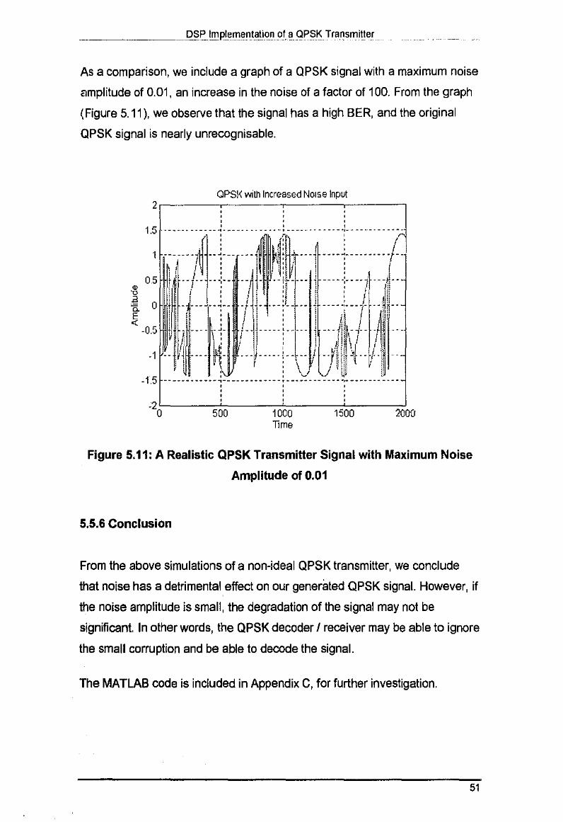
Page 1
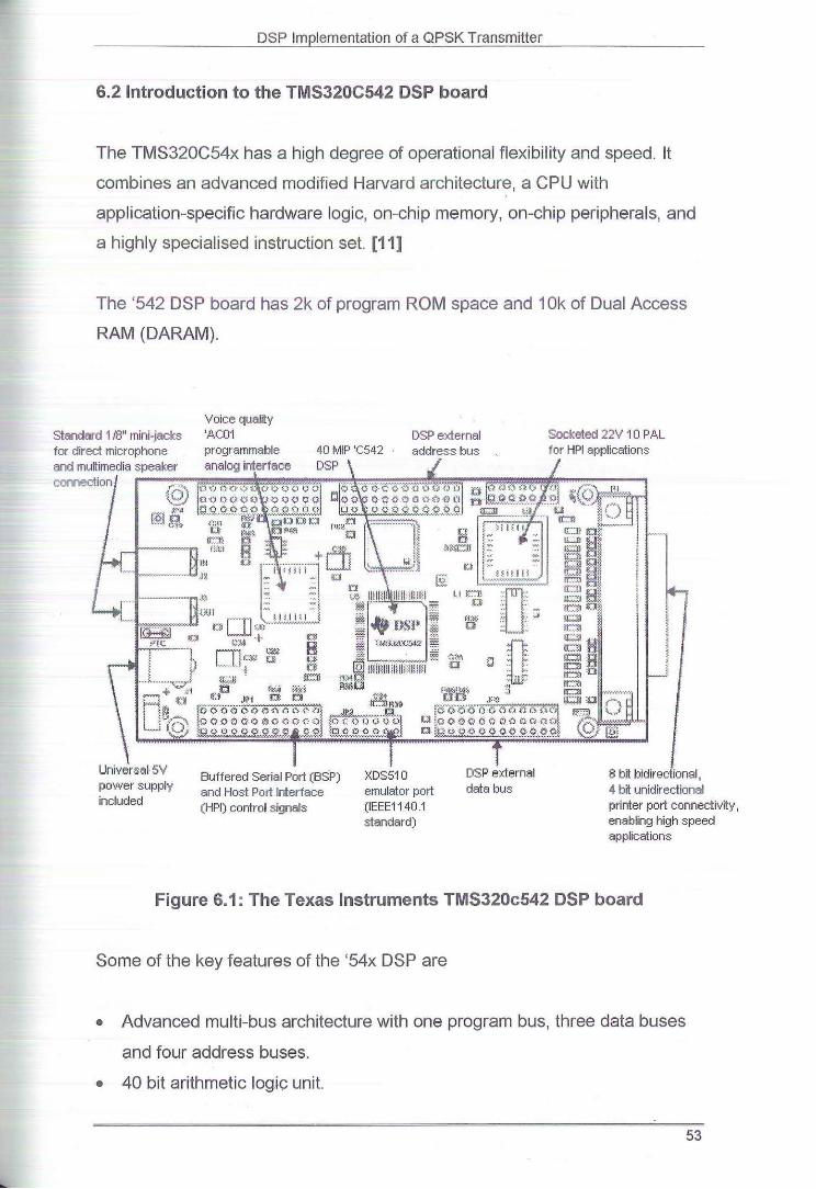
Edith Cowan University Edith Cowan University
Research Online Research Online
Theses : Honours Theses
1998
DSP implementation of a quadrature phase shift keying DSP implementation of a quadrature phase shift keying
transmitter transmitter
Andrew Phoon Edith Cowan University
Follow this and additional works at: https://ro.ecu.edu.au/theses_hons
Part of the Signal Processing Commons
Recommended Citation Recommended Citation Phoon, A. (1998). DSP implementation of a quadrature phase shift keying transmitter. https://ro.ecu.edu.au/theses_hons/471
This Thesis is posted at Research Online. https://ro.ecu.edu.au/theses_hons/471
Page 2
Edith Cowan University
Copyright Warning
You may print or download ONE copy of this document for the purpose
of your own research or study.
The University does not authorize you to copy, communicate or
otherwise make available electronically to any other person any
copyright material contained on this site.
You are reminded of the following:
Copyright owners are entitled to take legal action against persons who infringe their copyright.
A reproduction of material that is protected by copyright may be a
copyright infringement. Where the reproduction of such material is
done without attribution of authorship, with false attribution of
authorship or the authorship is treated in a derogatory manner,
this may be a breach of the author’s moral rights contained in Part
IX of the Copyright Act 1968 (Cth).
Courts have the power to impose a wide range of civil and criminal
sanctions for infringement of copyright, infringement of moral
rights and other offences under the Copyright Act 1968 (Cth).
Higher penalties may apply, and higher damages may be awarded,
for offences and infringements involving the conversion of material
into digital or electronic form.
Page 3
DSP Implementation of a Quadrature Phase Shift Keying
Transmitter
A Thesis Submitted in Partial Fulfilment of the Requirements for
the Degree of Bachelor of Engineering (Communications Systems)
Andrew Phoon
November 1998
Principal Supervisor: Dr. Ganesh Kothapalli
Faculty of Communications, Health and Science School of Engineering and Mathematics
Edith Cowan University Western Australia
Page 4
USE OF THESIS
The Use of Thesis statement is not included in this version of the thesis.
Page 5
I certify that this thesis does not incorporate without acknowledgment any
material previously submitted for a degree or diploma in any institution of
higher education; and that to the best of my knowledge and belief it does not
contain any material previously published or written by another person except
wh!lre due reference is made in the text.
Si~n~ure
Date
.?..''if ~.' .. /4S ....
Page 6
Edith Cowan University
Library I Archives
Use of Thesis
This copy is the property of Edith Cowan University. However, the literary
rights of the author must also be respected. If any passage from this thesis is
quoted or closely paraphrased in a paper or written work prepared by the
user, the source of the passage must be acknowledged in the work. If the
user desires to publish a paper or written work containing passages copied or
closely paraphrased from this thesis, which passages would in total constitute
an infringing copy for the purpose of the Copyright Act, he or she must first
obtain the written permission of the author to do so.
Page 7
Abstract
The aim of this project is to develop a DSP implementation of a QPSK
transmitter. This transmitter is to process digital signals in real-time and
modulate it with sinusoidal and cosinusoidal signals to produce the required
QPSK waveform.
This thesis is mainly divided into three sections. The first section deals with
the theory of modulation. Phase shift keying, in particular binary phase shift
keying, is explained in some detail, with references to the generation of
quadrature phase shift keying. In the second section, a brief overview of the
SIMULINK package from MATLAB is given, as simulations of ideal and non
ideal QPSK transmitters are to be conducted using SIMULINK. The first
simulation trial will be analysed and compared with the theory of PSK
transmitter with an introduction to the Texas Instruments TMS320x542 Digital
Signal Processor, and all program codes relating to the generation of BPSK.
An implementation of a Quadrature Phase Shift Keying (QPSK) transmitter
will be developed using two TMS320x542 Digital Signal Processors, with all
necessary modifications to the DSP codes.
The simulation and DSP implementation results are substantiated by
comparison with the theory of PSK modulation.
Page 8
Acknowledgments
I would like to extend my thanks and appreciation to Dr. Ganesh Kothapalli for
his supervision, encouragement, help, and motivation throughout this project.
I also like to thank my family, especially my wife, Jacqueline, for her love,
patience and understanding for the last 4 years.
II
Page 9
Table of Contents
1 Introduction 1
1.1 Motivation of the Thesis 1
1.2 Outline of the Thesis 1
2 Theory of Phase Shift Keying 3
2.1 Theory of Modulation 3
2.2 Phase Shift Keying 3
2.3 Bandwidth of Phase Shift Keying Signals 9
2.4 Phase Shift Keying Hardware Considerations 10
2.4.1 Balanced Modulator 10
2.4.2 Phase Shift Keying Detection 11
3 Quadrature Phase Shift Keying 13
3.1 Introduction to Quadrature Phase Shift Keying 13
3.2 Quadrature Phase Shift Keying Hardware Considerations-
Transmitter 17
4 Binary and Quadraiure Phase Shift Keying Error Performances 19
4.1 Introduction 19
4.2 Probability of Bit Error for Binary Phase Shift Keying 22
Ill
Page 10
4.3 Probability of Bit Error for Quadrature Phase Shift Keying 27
5 Simulation of a Quadrature Phase Shift Keying Transmitter 28
5.1 Introduction 28
5.2 SIMULINK Overview 28
5.3 QPSK Transmitter Design In SIMULINK 29
5.4 Description of the SIMULINK Block Diagram of a
QPSK Transmitter 30
5.5 Simulation Trials 31
5.5.1 Trial 1 33
5.5.2 Analysis of Simulation Trial1 36
5.5.3 Further Simulation Trials 37
5.5.4 Simulation of a Non-Ideal QPSK Transmitter 46
5.5.5 Analysis of the Non-ideal QPSK Transmitter
Simulation
5.5.6 Conclusion
6 DSP Implementation of a QPSK Transmitter
6.1 Introduction To DSP
6.2 Introduction to the TMS320C542 DSP board
48
51
52
52
53
iv
Page 11
6.31mplementation Considerations 54
6.3.1 Method One 54
6.3.2 Method Two 56
6.3.3 Method Three 56
6.4 DSP Code 57
6.5 Filtering 57
6.6 Window Functions 59
6. 7 DSP Code Description 60
6. 7.1 First Phase 61
6.7.2 Second Phase 63
6. 7.3 Third Phase 64
6.8 Description of the psk1_main.asm Code 64
6.9 DSP Hardware Implementation 68
7 Conclusions and Further Development 73
7.1 Conclusion of the Thesis 73
7.2 Further Considerations and De\ ,,;,)pment 73
7.3 Areas of Further lnvestigatior, 74
v
Page 12
Significant References
APPENDICES
Appendix A: A MATLAB SIMULINK Simulation of an Ideal
BPSK Transmitter
Appendix B: A MATLAB SIMULINK Simulation of an Ideal
QPSK Transmitter
Appendix C: A MATLAB SIMULINK Simulation of a Non-Ideal
75
77
80
QPSK Transmitter 83
Appendix D: Digital Recorder for the First
Memory Location (OOIOOh to 01 b80h) 92
Appendix E: Digital Recorder for the Second
Memory Location (01b81h to 027ffh) 95
Appendix F: DSP Code for BPSK Generation (Sine Carrier) 98
Appendix G: DSP Code for BPSK Generation (Cosine Carrier) 98
Appendix H: AC01 Initialisation Routine 1 04
Appendix 1: The Vector Table Initialisation 106
Appendix J: The Bandpass Filter Coefficients using
Blackman Filter\ .ndowing 108
vi
Page 13
DSP Implementation of a QPSK Transmitter
1 Introduction
1.1 Motivation of the Thesis
We understand that modulation and demodulation techniques are key
requirements in telecommunications and to be able to process information
practically we need tools that are effective. One important tool is Digital Signal
Processing (DSP). This is the basis of the project.
The aim of this project was to develop a DSP implementation of a Quadrature
Phase Shift Keying Transmitter.
This thesis presents an original work in the design and implementation of a
QPSK transmitter firstly via simulation using MATLAB's SIMULINK and finally
using Texas Instruments Digital Signal Processing boards. The DSP
transmitter is capable of generating real-time QPSK signals.
The MATLAB's SIMULINK function blocks were used to implement simple
functions needed in the simulation and development of the transmitter. The
predefined SIMULINK blocks were more than adequate in the transmitter
construction.
1.2 Outline of the Thesis
The outline of the thesis is as follows:
• Chapter 2 deals with the theory of modulation, Phase Shift Keying,
coherent and non-coherent PSK and the foundation required to
comprehend how PSK is achieved. It also outlines the hardware
considerations of PSK.
1
Page 14
--------------~D~S~P~Im~p~le~m~e~n~ta~tio~n~o~f~a~Q~P~S~K~T~m~n~sm~,~·ue~r--------~----~-
• Chapter 3 describes the theoretical concepts of QPSK. This includes the
hardware considerations for QPSK.
• Chapter 4 provides insight into error performances of both Binary and
Quadrature PSK, providing adequate statistical theory and bit error rates.
This chapter also compares the bit error probability of several binary
modulation and demodulation systems.
• Chapter 5 examines the design and simulation of an ideal and a non-ideal
QPSK transmitter using the built-in function blocks from MATLAB's
SIMULINK. It also provides the results of the analysis of the simulations.
• Chapter 6 provides detail on the DSP implementation of the QPSK
transmitter with introduction to the Texas Instruments DSP processor and
implementation considerations.
• Finally, Chapter 7 concludes the thesis by summarising the major
outcomes and includes recommendations necessary to improve on the
project.
2
Page 15
DSP Implementation of a QPSK Transmitter
2 Phase Shift Keying
2.1 Theory of Modulation
Before we examine the concepts of Quadrature Phase Shift Keying or QPSK,
we need to understand the foundations of modulation. Modulation is the
process where the digital symbols of a source signal are converted to
waveforms that are compatible with the transmission channel. In the case of
baseband modulation, these waveforms are pulses, but in bandpass
modulation, the desired information signal (the modulating signal) modulates
a sinusoid called a carrier wave, resulting in a modulated signal. As an
example, for radio transmission the carrier is converted to an electromagnetic
wave for propagation to the desired destination.
There are 3 basic types of modulation for the conversion of the hi nary signal
(or digital symbol). They are:
1) Amplitude Shift Keying
2) Phase Shift Keying
3) Frequency Shift Keying
Only two levels (high and low to represent logic 1 or 0) are required, as it is
only binary signals that need to be transmitted. Therefore, the signal shifts (or
switches) between these two levels as the binary signal stream changes
between 1 and 0. [1]
2.2 Phase Shift Keying
In this type of modulation, the frequency and the amplitude of the carrier wave
or signal is kept constant. It is the phase of the carrier signal that is being
shifted in phase as each bit in the data signal stream is transmitted.
3
Page 16
DSP Implementation of a OPSK Transmitter ------
It must be mentioned that bandpass modulation and demodulation is also
separated into two basic categories, which are coherent and non-coherent.
Note that the process of demodulation involves the detection of the baseband
information, and digital demodulation requires the help of reference
waveforms. The process is called coherent when the references contain the
entire signal attributes, especially phase. When the phase information is not
used, then the process is non-coherent. [2)
One example of non-coherent bandpass modulation/demodulation is
Differential Phase Shift Keying, DPSK. DPSK utilises the phase information of
the prior symbol as a phase reference for detecting the current symbol.
Bandpass Modulation!Oemo.dulation
Phase 5hift keying IPSK)
Frequency shift keying iFSK)
Amplitude shift keying (ASK)
Continuous nhase modulation (CPM)
Hybrids
Differential phase shift keying (DPSK)
Frequen"y shift keying (FSK)
Amplitude shift keying {ASK}
COntinuous phnse modulation ICPM)
Figure 2.1: Bandpass Modulation/Demodulation
Extracted from p128 Sklar B. (1988). Digftal Communications Fundamentals and Applications. Englewood Cliffs, New Jersey: Prentice-Hall
4
Page 17
DSP Implementation of a CPSK Transmitter
The figure below (Figure 2.2) shows the difference between coherent PSK
and DPSK.
ja) i l ! 1 0 ' I I 0 " I '
·-·-··-- .. ,._,_ f.--·····
' i i
+I II I\ II II 1\ II I\ .. .. . ..... .. .
-1 v v v v IJ I
v i v II II M II !II II liM ' .. . - ..
\1 v "" \J IJ, v 1~ v J. v IB<l" 1 RCr' .,.
It ~~~ ! II: II ~ i
l'hiiSl: Vf'Sp;(l} cohcttn!
v I v -~ Y,. v ,,. v ~7<r~ ,.. 110° 90"'
(b)
Signal llllW~r
.
I I I \ • & ~ • • • • • . . . ' . . . . • • • • • • • • . . . .
I 0 o o . . ' . • • • • .... L .. I... ...... L... ~ ;
!, ~ 1fo f~-!,. J~ .!~ + 11 f.+ ·.1~,
in= F'unda.mcntnl frcqutnc)' ~.'lmponcnt = Jll bit ra~ ~H~.J
(~) f.) ({)uudraturd
180".;:1) <r=l
i II
I
'
'
~ I
~ '
1------J.-----... I ,. llinphase)
Figure 2.2: Phase Shift Keying
Til1lC. I
a) Principle of Operation; b) Bandwidth Aftematives; c) Phase Diagram
Extracted from p65 Halsall, F. (1995). Data Communications, Computer Networks and Open Systems (4'" Ed.) England: Addison-Wesley
The first uses two fixed carrier signals to represent a binary 0 and 1 with a
180' phase difference between them. The disadvantage of this is that a
reference carrier signal is required at the receiver against which the phase of
the received signal is compared. However, with the DPSK, phase shifts occur
5
Page 18
at each bit transition regardless of whether a string of binary 1 s or Os is
transmitted. A phase shift of 90" relative to the current signal indicates a
binary 0 is the next bit while a phase shift of 270" indicates a binary 1. [1]
The general analytic expression for PSK is
[2E s, (t) = Vr cos[ro"t +¢,(I)] , (Eq. 1)
O~t~T,andi=1 ... M
where the phase term, .P,(t), will have M discrete values. The phase term is
given by
"' ( ) 2tri '1'1 t = --M (Eq. 2)
where i = 1 ... M. [2]
For the binary PSK (BPSK) example in the Figure 2.3 below, M is 2. The
parameter E is the symbol energy, Tis the symbol time duration and
O~t~T.
Analytic
PSK I• 1, 2 .. , .. M O~tST
~1\1\NI~ ~MI\1\~ lfV 0 lflfV lfV1J •-r-+r-+ ·T--j
Figure 2.3: PSK Analysis
Vllctcr
Extracted from p129 Sklar B. (1988). Digfta/ Communications Fundamentals and Applications. Englewood Cliffs, New Jersey: Prentice-Hall
6
Page 19
-~------ _____________ QSP __ !~pLe~e~t_ati~m ~fa QPSK Tr_ansmit!er
Now let a pair of signals s,(t} and s2(t} be used to represent binary symbols 1 and 0 respectively. In BPSK, they are represented by
(2f.; s, (I) ~ vr: cos(2;if,./) (Eq. 3)
g ~ s, (I)= vr: cos(2,yJ + Jr) (Eq. 4)
Or g
s, (/) = -vr: cos(21ff,t) (Eq. 5)
where 0 515 To, and E• is the transmitted signal energy per bit.
In order to ensure that each transmitted bit contains an integral number of
cycles of the carrier wave, the carrier frequency fc is chosen equal to ncl Tfor
some fixed integer nc. [3]
Binary waveforms that are the negative of one another, such as the bipolar
pair above, where s1(t) = - s2(t) are known as antipodal signals. [2]
If we let
¢, (t) = (2 cos(2'!fi) vr: 0515T,
we then can represent st(t) and s,(t) as follows:
s1(/) = JE ·¢,(I)
s,(t)=-.fE·¢2(1)
(Eq. 6)
(Eq. 7)
(Eq. 8)
7
Page 20
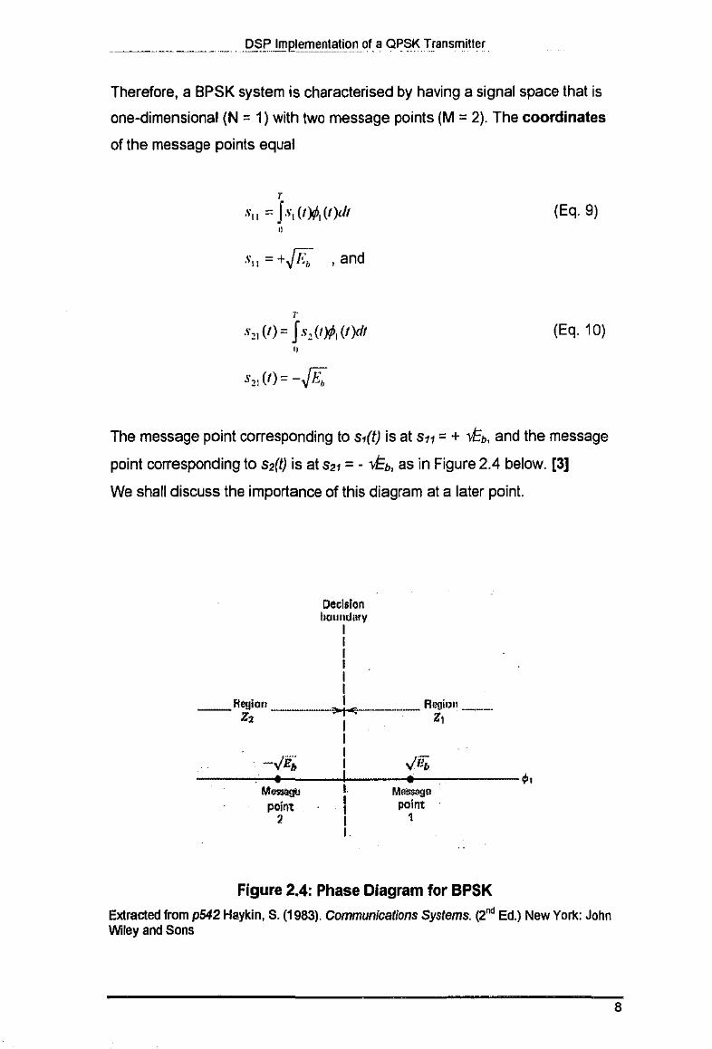
Therefore, a BPSK system is characterised by having a signal space that is
one-dimensional (N = 1) with two message points (M = 2). The coordinates
of the message points equal
,. s 11 = Js,. (1)¢1 (t)dt (Eq. 9)
" ·'\ 1 = +.JE: , and
,. s 01 (1)= Js,(t)¢1(/)dl (Eq. 1 0)
" s, (/) = -.JE,.
The message point corresponding to 5,(1) is at 511 = + J: •. and the message
point corresponding to 52(1) is at 52t = - J: •. as in Figure 2.4 below. [3]
We shall discuss the importance of this diagram at a later point.
Decision houm.lary
I I I I I I
_f!~on ____ l.,.._ _________ A~1ion ____ _
-..;e• ------~.-----~----_.-----------~\
M""""" I point I
2 I I
Ma$1ga point
1
Figure 2.4: Phase Diagram for BPSK
Extracted from p542 Haykin, S. (1983). Communications Systems. (2"' Ed.) New York: John Wiley and Sons
8
Page 21
As a summary, in BPSK modulation, the modulating data signal shifts the
phase of the waveform, s;{t), to one of two states, either zero or"· The
waveform sketch in Figure 2.2 shows a typical BPSK waveform with its abrupt
phase changes at the symbol transitions. Also the signal waveforms can be
represented as vectors on a polar plot where the length of the vector
corresponds to the amplitude of the signal.
2.3 Bandwidth of Phase Shift Keying Signals
We can mathematically determine the bandwidth requirements of PSK by
representing the binary data signal in its bipolar form since the negative signal
level used with bipolar then results in a 180' phase change in the carrier. If we
assume that the amplitude is unity and the fundamental frequency is roo, a
bipolar periodic data signal can be represented by the Fourier series:
4 I I vd (I)= -{cosm01--cos3m01 +-cos5mof- ... )
n 3 5 (Eq. 11)
Hence:
4 I VPSK = -{ COSalJ' COSW0f- -COS(lJi 'C0S{t)0( + ... }
n 3 (Eq. 12)
2 I I = -(cos(m,- m0 )1 + cos(m, +m0 )1- -cos(m, -3m0 )t --cos(ru, + 3m0 )1 + ... )
1t 3 3
where me = 2 nfc and mo = 2 nfo.
The bandwidth of a PSK signal is shown in Figure 2.2(b) above. (1]
9
Page 22
2.4 Phase Shift Keying Hardware Considerations
The diagram below (Figure 2.5) shows how the digital signal is PSK
modulated.
Fig 1 Balanced Modulator
Carrier
DSBtPSK Out lllililllil
Phase
Figure 2.5: PSK Modulation
Extracted from Miller, J. (1995) The Shape of BNs to Come (on-line] Available ftp: ftp. amsat.org. amsat/articles/g3ru h/a 1 o .zip
2.4.1 Balanced Modulator
A balanced modulator consists of two AM modulators and an adder, as in the
diagram below (Figure 2.6).
JOCII - AM s111) modul1tor
os C2r/,tl +
Otcill.tor Er s C2r{,tl
- AM •2tl) moouiiiOf
··orb I
Figure 2.6: A Balanced Modulator
Extracted from p276 Haykin, S. (1989). An Introduction To .r.nalog and Digital Communlcafions New York: John Wiley and Sons
10
Page 23
The AM modulators are arranged in a balanced configuration to suppress the
carrier wave, and they are assumed to be identical in nature. The main
difference is that the modulating wave input to one of the modulators is sign
reversed. The outputs of the modulators can be expressed as:
s, (I)= AJI + k,m(l)]cos(2'1f.l)
and
Finally, we subtract s2(t) from st(t) resulting in
s(l) = s1 (I)- s2 (I)
s(l) = 2k ,A, cos(27ifJ)m(l)
Hence, the output s(t) is equal to the product of the modulating wave and the
carrier, except for the scaling factor of 2k •. [4]
2.4-2 PSK Detection
PSK signals must be detected synchronously because asynchronous
detection does not recognise phase shifts.
In demodulating a PSK signal, it is necessary to regenerate the carrier signal
at the receiver. This is accomplished by deriving the carrier signal from the
received PSK signal with a carrier synchroniser consisting of a frequency
doubler, a Phase-Lock-Loop (PLL) and a +2 and 90° phase shift circuitry.
11
Page 24
1-'!,;1< s= ..... v '''"''''"' ~: r~.d ----------- -:,.;~ "'ll"~· L I '" .. ·i;~''"~u-~y- 2-~rool ·r:J-ol-"11-
1 '''"~" ';holt
-~--~----- --------- l'h·""''"k'""''
I ~--i." ..... ____ __j
Figure 2. 7: Carrier Synchroniser
The first stage doubles the frequency of the incoming signaL In order to lock
the PLL, the VCO(Voltage Controlled Oscillator) OUT frequency must also be
twice the PSK signal frequency. The final stage of the carrier synchroniser
divides the PLL output signal by 2 and shifts it by 90° to produce the
regenerated carrier signaL The frequency of the regenerated carrier signal is
equal to the PSK signal frequency.
The regenerated carrier signal is then multiplied with the received modulated
signal, as in Figure 2.8.
x!t) I. Tb "' Decision \.~ 0 de device
Choose 0 if x1 < 0
~,(II
Figure 2.8: Recovering Digital Information (PSK)
Extracted from p544 Haykin, S. (1983). Communication Systems (2"' Ed.) New York: John Wiley and Sons.
We label the locally generated coherent reference signal as ¢1(t). So to
reconstruct the original binary data signal, we apply both these signals to a
correlator. The output of the correlator, x,, is compared with a threshold of
zero volts. If (x1 > 0), the receiver decides in favour of symbol1. Inversely, if
(x, < 0), then the receiver decides in favour of symbol 0. [3]
12
Page 25
3 Quadrature Phase Shift Keying
3.1 Introduction to Quadrature Phase Shift Keying (QPSK)
The primary objective of spectrally efficient modulation techniques is to
maximise bandwidth efficiency, defined as the ratio of data rate to channel
bandwidth (bps I Hz). [3]
One of the techniques is the Quadrature Phase Shift Keying (QPSK}, which is
an extension of BPSK.
As with binary PSK, this modulation scheme is characterised by the fact that
the information carried by the transmitted wave is in the phase of the wave.
However, in a QPSK wave, the phase of the carrier has four possible values,
s,(t) = {ff co{ 27!fJ+(2i -I):]}, 0 5t 5T, (Eq. 13)
where i = 1 ,2,3,4, and E is the transmitted signal energy per symbol, Tis the
symbol duration and the carrier frequency f, equals n,l T for some fixed
integer n,. [3]
In a QPSK system, we note that there are two bits per symbol, which means
that the transmitted signal energy per symbol is twice the signal energy per
bit. In other words,
E=2E•
By analysing the equation, we observe that there are four possible values for
the phase, which are x/4, 3x/4, Sx/4 and 7x/4. By using a trigonometry
identity, we can expand the mathematical expression above to be:
13
Page 26
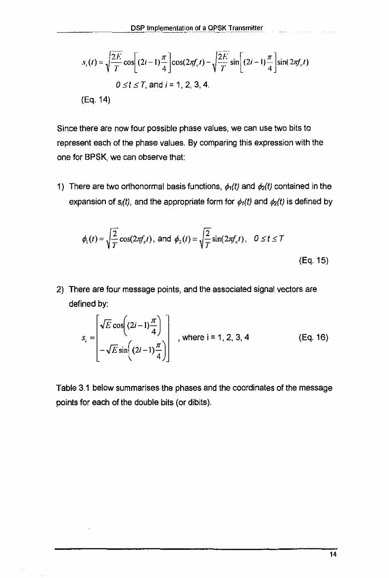
.1, (I) = J2/; co{(2i- I): ]cos(21ff..t)-J2/; sin[(2i- I):] sin( 2nfJ)
0 5ts T, and i = 1, 2, 3, 4.
(Eq. 14)
Since there are now four possible phase values, we can use two bits to
represent each of the phase values. By comparing this expression with the
one for BPSK, we can observe that:
1) There are two orthonormal basis functions, r/!1(1) and (I,( f) contained in the
expansion of s;(f), and the appropriate form for ¢t(f) and (!,(f) is defined by
¢,(1)=Hcos(2nfJ), and ¢2 (1)=Hsin(2nf,1), 0515T
(Eq. 15)
2) There are four message points, and the associated signal vectors are
defined by:
s -,-,,E co{ (2i-l):) -,,E sin( (2i -I):)
, where i = 1, 2, 3, 4 (Eq. 16)
Table 3.1 below summarises the phases and the coordinates of the message
points for each of the double bits (or dibits).
14
Page 27
~~-------- ____________ DS~-l~~L~.f!l~ntat!~n. 9~_!1_9PSK Jran_smitter
Input dlhll OS:t<'l' ""· ""'·
10 00 01 II
Phnse of (jl'SK slgn•l
(radhuu)
Coordinates or message points
rr/4 Jrr/4 5rr/4 7n/4
Table 3.1
+JEIJ ··· !E/2
\: .--·· _ I r.;o \J •• -
+JEil
- J 1!/~ ·· IE/2 "'·---+ .jl!/2 tJE/2
Extracted from p554 Haykin, S. (1983). Communication Systems (2"d Ed.) New York: John Wiley and Sons.
A QPSK signal is accordingly characterised by having a 2 dimensional space
(N = 2) and four message points (M = 4), as in Figure 3.1. [3]
// Region z,
-MflSIQ! ,... -fl(lint a 1
fdibltOll I
'
Qec:islon boundary
- --....... , Rttion z. ..;m
-- _, MelSo\1111 1 polnt4 I (dibit 11)
0 ' :fi.il ' __ _.
M~ Region point 1 z
ldibit 101 / •l
/ .. --·
Oetil.ion bound;~ry ..... '>1
Figure 3.1: Signal Space Diagram for QPSK
Extracted from p554 Haykin, S. (1983). Communication Systems (2"" Ed.) New York: John Wiley and Sons.
15
Page 28
_ ----------~D~S~P Implementation of a QPSK T~~ns'!!_i!~~-r _________________ _
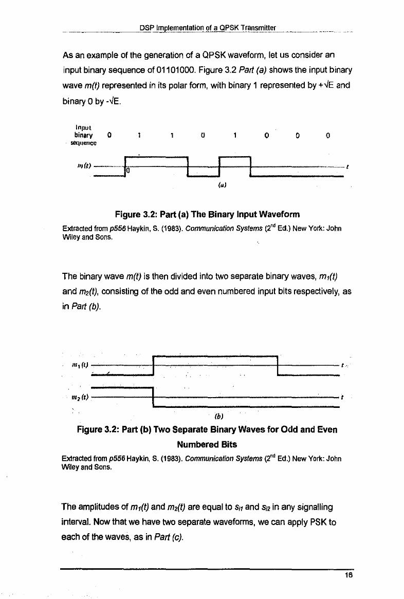
As an example of the generation of a OPSK waveform, let us consider an
input binary sequence of 01101000. Figure 3.2 Part (a) shows the input binary
wave m(l) represented in its polar form, with binary 1 represented by +..JE and
binary 0 by -..JE.
Input binarv 0 1 1 0 1 0 0 0
SoeCIIlt!!ICO
".rn--······Jr I I I ----+--t---t-------·············-1
(a)
Figure 3.2: Part (a) The Binary Input Waveform
Extracted from p556 Haykin, s. (1983). Communication Systems (2"' Ed.) New York: John Wiley and Sons.
The binary wave m(l) is then divided into two separate binary waves, m,(t)
and m2(t), consisting of the odd and even numbered input bits respectively, as
in Part (b).
m1(t) ~----:---11---~--------t------t.
•r2 1t).------+----------------'--• (b)
Figure 3.2: Part (b) Two Separate Binary Waves for Odd and Even
Numbered Bits
Extracted from p556 Haykin, S. (1983). Communication Systems (2"' Ed.) New York: John Wiley and Sons.
The amplitudes of m,(t) and m2(l) are equal to S;r and S12 in any signalling
interval. Now that we have two separate waveforms, we can apply PSK to
each of the waves, as in Part (c).
16
Page 29
.. , too, r•l }'\vf'\;':\J\/\/\/:f\J\.., , It)·• (<)6 ~ A A A I\..?' , ··v ~\JV
lei
::igure 3.2: Part (c) PSK waves m1(t)(J,(t) and mz(tj¢J2(t)
Extracted from p556 Haykin, S. (1983). Communication Systems (2nd Ed.) New York: John Wiley and Sons.
Finally, we just add the two binary PSK waveforms m,(t}(>,(t) and mz(t)th(t)
together, producing the QPSK wave, s(t) = m,(t}(J,(t) + m,(t),P,(t). [Part (d)].
( 1\ !\ ~. 1\ 6 6 n 6 1\ st)}-v \J\J\)\JV'\J\T\'
(d)
Figure 3.2: Part (d) QPSK Wave s(t)
Extracted from p556 Haykin, S. (1983). Communication Systems (2"' Ed.) New York: John Wiley and Sons.
3.2 QPSK Hardware Considerations - Transmitter
The diagram below (Figure 3.3) shows the block diagram of a typical QPSK
transmitter. The input binary sequence is presented in polar form. The bits 1
and 0 are represented as +-./E and --./E respectively. This binary wave is then
divided by using a demultiplexer into two separate binary waves consisting
of odd and even numbered input bits, denoted by m,(t) and m,(t).
17
Page 30
- ---------------- --- --------- o~p_ __ !!11P1e_~e~_l~t_i91_1 O! a _QP~K Tran~mitter
II'IJ~Ut blnif"V wave m(tl
,.,, {l)
Demultipl~xHr
+
m:~ {tl '-----.o{X)--...1
Figure 3.3: A QPSK Transmitter
Extracted from p560 Haykin, S. (1983). Communication Systems (200 Ed.) New York: John Wiley and Sons.
The two binary waves m,(l) and m2(1) are then used to modulate a pair of
quadrature carriers ¢,(1) and ¢2(1). The result is then 2 binary PSK waves,
which is detected independently due to the fact that (1,(1) and ¢211) are
orthogonal to each other. Lastly, the two BPSK waves are added to produce
the QPSK wave. The symbol duration, T, of a QPSK wave is actually twice as
long as the bit duration, r., of the input binary wave. This show that for a
given bit rate, 1/ To, the QPSK wave requires half the transmission bandwidth
of the corresponding BPSK wave. In other words, a QPSK carries twice as
many bits of information as the corresponding binary PSK wave for a given
transmission bandwidth. [3]
18
Page 31
..... __ f?_§_~_l!!_l~l~_m.~n!a_t_iQn_ ~fa QPS~_Transmitter
4 Binary and Quadrature Phase Shift Keying Error
Performances
4.1 Introduction
Before we can fully understand the error performance of BPSK and QPSK, we
need to examine the basics of noise and the detection of binary signals in
noise.
Once the digital symbols are transformed into electrical waveforms, they can
then be transmitted through the channel. During a given interval, T, a binary
system will transmit one of two waveforms, s,(t) or s2(t). The transmitted
signal over the interval (0, 7) is represented by s;(t).
The signal, r(t), received by the receiver is represented by
r(l)=s,(t)+n(l) i=1,2 OstsT (Eq. 17)
where n(t) is a zero-mean additive white Gaussian noise (AWGN) process.
There are two separate steps involved in signal detection. The first step is to
reduce the received waveform, r(t), to a single number, z(t = T). This
operation can be performed by using a linear filter and a sampler. The output
gives the sample, z(T), also called the test statistic.
z(7') = a1 (7') + n0 (T) i = 1 2 '
(Eq. 18)
where a;(T) is the signal component of z(T) and no(T) is the noise component.
Since the noise component, n0(T) is a zero-mean Gaussian random variable,
this makes z(T) a Gaussian random variable with a mean of either a1 or a2
depending on the binary symbol that was sent. The probability density
function (pdf) of the Gaussian random noise, no is
19
Page 32
DSP Implementation of a QPSK Transmitter
[ ( )'] I I 1111 p(n,)~ exp -- -cr.J21r 2 cr0
(Eq. 19)
where cr2 is the noise variance.
By replacing no in the formula above with no ~ z- a1, we get the conditional
pdfs of s, and s2:
[ ( )'] I I ·-a p(zJs,)~ =exp -;:- _._,
a 0 -v2;r 2 0'0
(Eq. 2C)
[ ( )'] I I • -a p(z J s2 ) ~ r,;-cxp -- • 2
Un"V27r 2 a0
(Eq. 21)
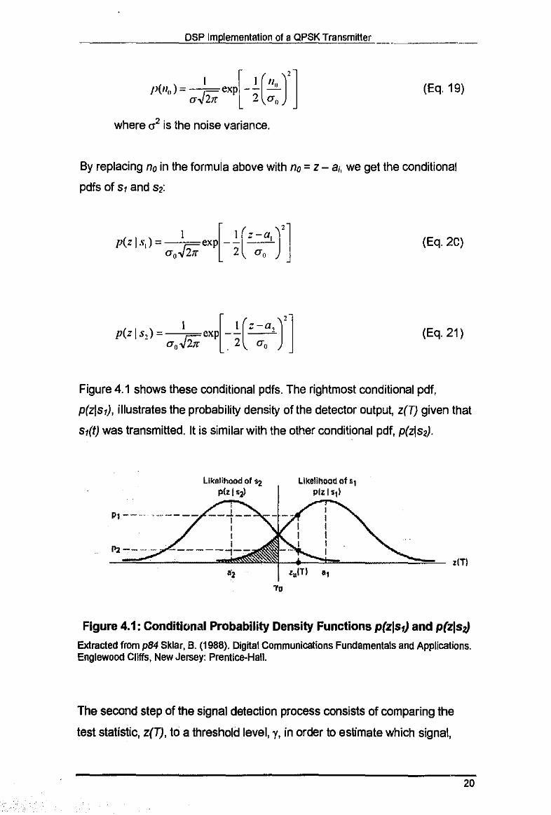
Figure 4.1 shows these conditional pdfs. The rightmost conditional pdf,
p(zJs,), illustrates the probability density of the detector output, z(T) given that
s,(t) was transmitted. It is similar with the other conditional pdf, p(zJs2).
""-- '" '"
LikBiihood of '2 p{z I s2)
Likelihood cf s1 plzl s11
ziTI ., .,
Figure 4.1 : Conditional Probability Density Functions p(zJs,J and p(zJsv
Extracted from p84 Sklar, B. (1988). Dignal Communications Fundamentals and Applications. Englewood Cliffs, New Jersey: Prentice-Hall.
The second step of the signal detection process consists of comparing the
test statistic, z(T), to a threshold level, y, in order to estimate which signal,
20
Page 33
DSP Implementation of a QPSK Transmitter
5,(1) or 82(l) has been transmitted. Obviously, choosing the threshold level, y,
for the binary decision is based on minimising the probability of error. For
equally likely signals, the optimum threshold, yo, passes through the
intersection of the likelihood functions, as shown in Figure 4.1.
There are 2 ways that an error can occur, based on Figure 4.1. An error, e,
will occur when 5,(1) is sent, and channel noise results in the receiver output
signal, z(T), is less than y0 . The probability of such an occurrence is
lo
P(els,)=l'(H, Is,)= jp(zls,)dz (Eq. 22)
-· This is the shaded area to the left of yo in Figure 4.1. This is similar in the
opposite case, where a signal 5 2(1) is sent, and due to the noise, z(T) is
greater than yo. The probability of this occurrence is
• P(e I s2) = P(H, Is,)= f p(z I s,)dz , (Eq. 23)
lo
where H, and H2 are the two possible (binary) hypotheses. (Choosing H1 is
equivalent to deciding that 51{1) was sent, and choosing H2 is equivalent to
deciding that 52(1) was sent).
The probability of an error is the sum of the probabilities of all the ways thai
an error can occur. For the binary case, the probability of bit error, P8 , is:
2
1'8 = LP(e,s,) 1=1
By combining Eq. 22 with the equation above, we get
1'8 = P(e I s,)P(s1)+P(e I s,)P(s,),
or equivalently,
P8 =P(H,Is,)P(s1)+P(H1 1,2)P(s2 )
(Eq. 24)
(Eq. 25)
(Eq. 26)
21
Page 34
_______ D"S"'P-"'tm,.,p,_tem=•n,ta,ti,on,__,of a QPSK Tra~.J!lJ~!E:!.~--~----~----·---------
That is, given a signal st(t) was transmitted, an error results if H, is chosen; or
given a signal s2(1) was transmitted, an error results if H, was chosen. [2]
4.2 Probability of Bit Error for Binary Phase Shift Keying
Now let us examine the BPSK system. In Figure 2.4, we see that there are
two regions and a decision boundary separating the two message points, to
satisfy the decision rule. In other words, to realise the decision rule, we must
partition this signal space into two regions,
1) The set of points closest to the message point at +vE.
2) The set of points closest to the message point at -..JE.
The decision rule is referred to as maximum likelihood, and the device for its
implementation is called the maximum likelihood decoder. This decoder
computes the metric for each transmitted message, compares them, and then
decides in favour of the maximum.
Now a mid-point line is constructed (the decision boundary) and the decision
regions are marked (region Z1 and Z,). The decision rule is to guess s,(t) or
binary symbol1 was transmitted if the received signal point falls in region Z1,
and guess signal s2(t) or binary symbol 0 was transmitted if the received
signal point falls in region Z2.
As described above, two kinds of errors will be made. Signal s1(t) is
transmitted, but the noise can be such that the received signal point falls
inside region Z2 and so the receiver decides in favour of s,(t). The opposite
situation can also happen, where the signal s2(t) is transmitted, but due to the
noise, the received signal falls in the Z1 region.
Again, to calculate the probability of a bit error, P8 , we use the equation:
P8 = P(H 2 I s,)P(s,) + P(H, I s,)P(s2 ) (Eq. 26)
22
Page 35
For the case when P(s1) = P(s2) = 0.5, we get
I I 1'11 =?.P(II, ls,)+ZP(II,Is,) (Eq. 27)
Since the probability density functions are symmetrical, we can observe that
(Eq. 28)
This shows that the probability of a bit error, P8 , is numerically equal to the
area under the 'tail' of either pdf that falls on the 'wrong' side of the threshold.
We can therefore calculate Ps by integration of either p(zls,) or p(zjsz).
Region 2
l.ike!ihoot.i o! s7 plz I s;.ol
Decision lin~:
negion 1
Likelihood of s1 p{i! t s1l
<.11 .... ill 10 = 2 •0
Figure 4.2: Conditional Probability Density Functions (BPSK)
Extracted from p137 Sklar, B. (1988). Digital Communications Fundamentals and Applications Englewood CIHfs, New Jersey: Prentice-Hall.
For example, in Figure 4.2, we integrate 00
J p(z I s,)dz (Eq. 29)
The equation can be expanded to be:
I' J 1 1 z- a 2 00 [ ( J'] 8 :::: exp --
(a1+a1)J2uo5 2 Uo
(Eq. 30)
23
Page 36
DSP Implementation of a QPSK TransrT_Jitl_~-------
If we let
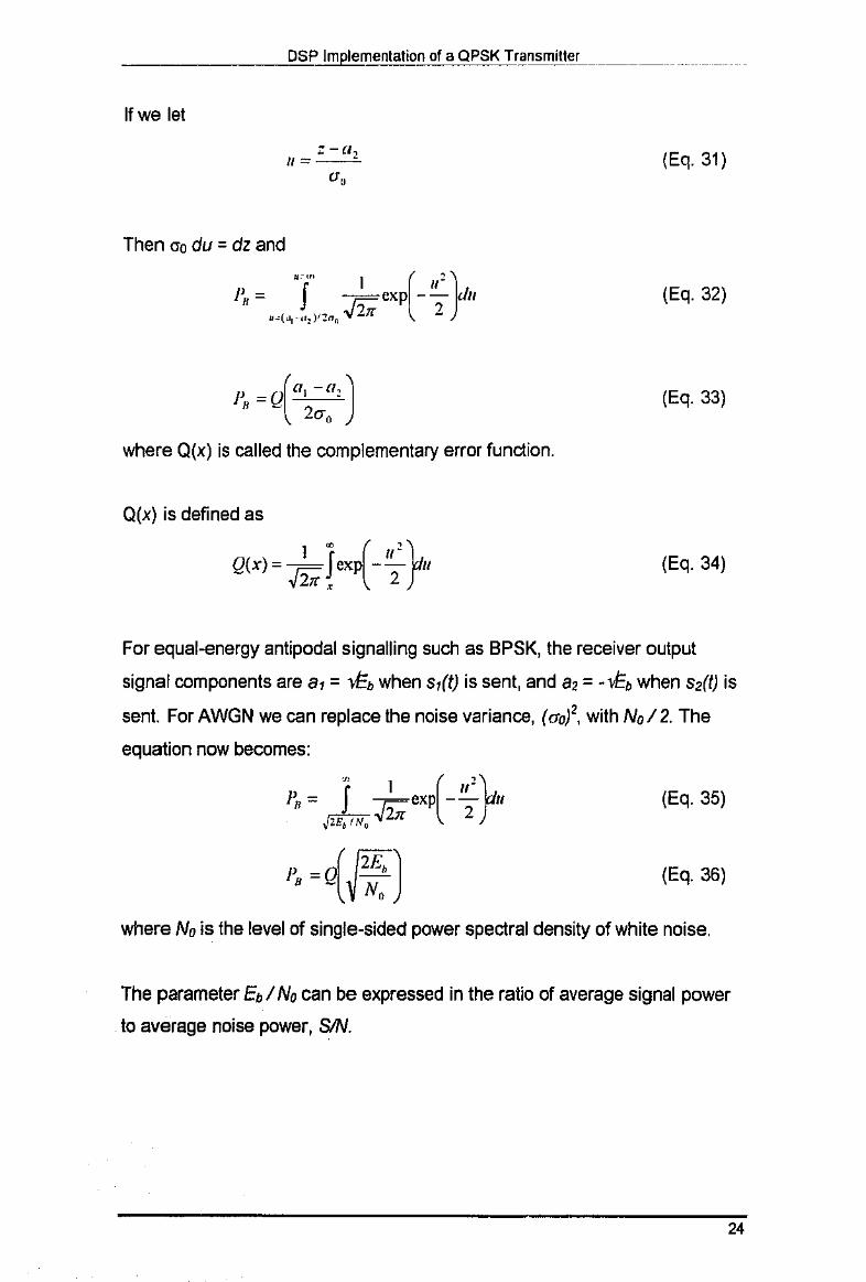
a,
Then cro du = dz and
,.,.. I [ u'J 1~1 = J --exp -- du u.o(~1 -<~:)'Zn0 J'2;; 2
1' =o("• -a,J H - 2 O'o
where Q(x) is called the complementary error function.
Q(x) is defined as
I • [ u' l, Q(x)= v!zff[exp -'2J"
(Eq. 31)
(Eq. 32)
(Eq. 33)
(Eq. 34)
For equal-energy antipodal signalling such as BPSK, the receiver output
signal components are a, = ...E. when s1(t) is sent, and a2 = - vt=. when s2(t) is
sent. For AWGN we can replace the noise variance, (cro!', with No/2. The
equation now becomes:
"' 1 [ "'} 1'8 = J r.;-exp -- u =v2Jr 2 , .. ,, .. (Eq. 35)
(Eq. 36)
where No is the level of single-sided power spectral density of white noise.
The parameter E. I No can be expressed in the ratio of average signal power
to average noise power, SIN.
24
Page 37
DSP Implementation of a QPSK Transm"'itte"!.r_
1\, st s sw s(w) -=-=--= =--N., N., liN., IIN,W N II
where S =average modulating signal power
T = bit time duration
R = 1rr =bit rate
N=No/W
W = signal bandwidth
(Eq. 37)
Figure 4.3 describes a system's error probability performance in terms of
available Eo! No. For Eo/ No ~xo, PE;; Po.
Figure 4.3: General Shape of P, versus Eo I No Curve
Extracted from p159 Sklar, B. (1988). Digital Communications Fundamentals and Applications Englewood Cliffs, New Jersey: Prentice-Hall.
The dimensionless ration Eo I No is a standard quality measure for digital
communications system performance. The smaller the required Eo I No, the
more efficient the system modulation is and the detection process for a given
probability of error.
25
Page 38
DSP Implementation of a QPSK Transmitter
Figure 4.4 compares the bit error probability, Pa, for several types of binary
modulation systems. In this diagram, the Shannon limit is shown. This limit
represents the threshold E• I No below which reliable communication cannot
be maintained. (2]
1 ...
10 I
.~ :5 10 J --
i • " 1o-< ~
ii5
1u··S ... ._
10
Nont:oherl!nt detection of FSK
CohcHmt dcl~'Ction/
PSK
"
Coherent detection of ,.. differentilllly encoded PSK
Diffi!IE:nti.llly coher~nt /
rl!!t~;:r.:tion ol ,.. diffrmmtially f':ncodftci PSK
(OP5K)
Shannon limit // 1-1.6dBJ
Cohen:mt / Lft:tection
"" FSK
Figure 4.4: Comparison Of Bit Error Probability of Several Binary
Modulation I Demodulation Systems
Extracted from p160 Sklar, B. (1988). Digital Communications Fundamentals and Applications Englewood Cliffs, New Jersey: Prentice-Hall.
26
Page 39
_______ _,D00SP'--"'Im.,.p,le"'m~encot.,.atiQ!! ~?.fa QPSK Transi!J_~!~f------~---- .. ~-----
4.3 Probability of Bit Error for Quadrature Phase Shift Keying
Again, QPSK can be characterised as two orthogonal BPSK channels. The
QPSK bit stream is usually partitioned into an even and odd (In-Phase, or(/),
and Quadrature, or (Q)) stream. Each new stream modulates an orthogonal
component of the carrier at half the bit rate of the original stream. The I
stream modulates the cos rual term and the Q stream modulates the sin rual
term. Now if the magnitude of the QPSK vector has the value A, then the
magnitude of I and Q component vectors will have v'A/2. Therefore, each of
the quadrature PSK signals has half of the average power of the original
QPSK signal. Hence, if the original QPSK waveform has a bit rate of R bits/s
and an average power of S watts, the quadrature partitioning results in each
of the BPSK waveforms having a bit rate of R/2 bitsls and an average power
of S/2 watts.
The Eo I No characterising each of the orthogonal BPSK channels is:
(Eq. 38)
This shows that each of the orthogonal BPSK signals, and hence the
composite QPSK signal has the same Eo I No and therefore the same Ps
performance as the BPSK signal. [2]
27
Page 40
5 Simulation of a Quadrature Phase Shift Keying Transmitter
5.1 Introduction
For this simulation, we do not have to be concerned about the noise aspect of
the system, since in the transmitter, we do not introduce noise. [However, we
do acknowledge that there is thermal noise within the transmitter itself].
MATLAB's SIMULINK is used for this simulation.
5.2 SIMULINK Overview
SIMULINK is a program for simulating dynamic systems. It is a visual
extension of MATLAB with many additional features specific to dynamic
systems while retaining all of MATLAB's general-purpose functionality. [5]
SIMULINK provides a visual interlace that gives a user the capacity to design
a system from user-defined or in-built blocks. These blocks can be connected
either by signal lines drawn by the user or by using special interconnecting
blocks, creating a block diagram of the desired system. By using the menu
bar at the top of the window, a simulation can be performed, monitored and
recorded. Scopes and graphs can be used to monitor the output of the system
designed. Also, the simulation results can be viewed in MATLAB by using the
workspace variables to store the contents of the output.
The in-built blocks in SIMULINK are available from a template library, which
contains a large selection of blocks from different categories. These blocks
represent analogue and digital circuits, filters, scopes, logic functions, and
more. By dragging and dropping the desired block onto the workspace, a
system can be easily assembled by the designer.
28
Page 41
I
5.3 QPSK Transmitter Design In SIMULINK
By using the in·biJilt blocks supplied by SIMULINK, we can design a simple
QPSK transmitter. For the first simulation run, we have chosen to include
several extra monitors to check the full functionality of this design (see Figure
5.1 ). These monitors are the workspace variables that store the data from
each signal line. Graphs are then plotted using the data acquired.
Figure 5.1: SIMULINK Representation of a QPSK Transmitter
29
Page 42
DSP Implementation of a QPSK T!.~-".~!!.ll!~E!r. ..... -~----------- ___ _
5.4 Description of the SIMULINK Block Diagram of a QPSK Transmitter
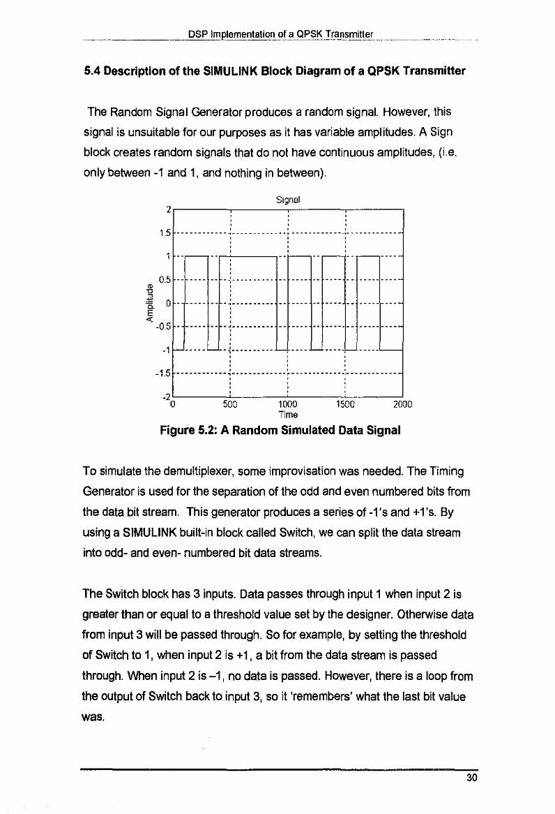
The Random Signal Generator produces a random signal. However, this
signal is unsuitable for our purposes as it has variable amplitudes. A Sign
block creates random signals that do not have continuous amplitudes, (i.e.
only between -1 and 1, and nothing in between).
Signal 2,-----~----~------~----.
1.5 ----------- -~----- -------- ~- ------------:------------' ' ' ' ' ' ' ' '
1 --,----- : --i----- ~·-- ,-------' ' ' 0.5 -- ---- -- +--------- -- ---- -- ---- -- ----------. '
~ ' " ' ~ 0 - ----- -- -~---------- -- ---- -- ---- -- ---------"- ' E ' <( :
-0.5 - ----- -- -~---------- -- ---- -- ------- ---------' '
-1------'- -~---------- -,---- L- -----1--------' ' ' ' ' ' ' ' '
-1.5 ------------ ~---------- --- ~---- ---------:-------------' ' ' ' ' ' ' ' ' ' ' ' -2:-----~~----~~----~~--~-0 500 1000 1500 2000
Time
Figure 5.2: A Random Simulated Data Signal
To simulate the demultiplexer, some improvisation was needed. The Timing
Generator is used for the separation of the odd and even numbered bits from
the data bit stream. This generator produces a series of -1 'sand +1 's. By
using a SIMULINK built-in block called Switch, we can split the data stream
into odd- and even- numbered bit data streams.
The Switch block has 3 inputs. Data passes through input 1 when input 2 is
greater than or equal to a threshold value set by the designer. Otherwise data
from input 3 will be passed through. So for example, by setting the threshold
of Switch to 1, when input 2 is +1, a bit from the data stream is passed
through. When input 2 is -1, no data is passed. However, there is a loop from
the output of Switch back to input 3, so it 'remembers' what the last bit value
was.
30
Page 43
_______ _,D=SP_!mplementation of a QPSK Tran§!!!~"~-~-C _________________ __________ ·-- ....
" u
T1mmg 2.--------.----~---,
·].5 --------.--- ~----- ----.-- -~----.---.-- •. :. --.- .. ---.--' ' ' ' ' ' ' ' '
1 -- -- -- i--- --,-- ,· --,-- ' 05 ---- -- ---- -- -- ---- -- ---- -- -- ---- -- ---- -
" j 0 - -- -- -- - -- -- ---- -- ---- -- -- - -- -- ---- -
-0.5 - -- -- -- - -- -- - -- -- ---- -- -- - -- -- ---- --
_., --1---- '-- -- ,-- '-- --' ' ' ' '
-1.5 ------------ ~-- ----- --· ---~-- --------- .. ; .... --------' ' ' ' ' ' ' ' ' -20':---~,----------::=---;;:';:;;--------;c;!
500 1000 1500 2000 Time
Figure 5.3: Output of the Timing Generator
In other words, the two switches (Switch and Switch1) act as sample-and-hold
for the data_
Now we have 2 streams of signals available to us: the In Phase stream (from
the odd-numbered bits) and the Quadrature stream (from the even-numbered
bits). Both data streams are then multiplied with modulating waveforms, one
90° out of phase with the other. The resultant waveforms are the BPSK
waves_ These two signals are then added together to form the QPSK wave_
5.5 Simulation Trials
Ten different samples of data were generated by the Random Signal
Generator. This was easily accomplished by changing the seed value of the
Generator. As mentioned previously, several extra monitors were added to
the design to check the full functionality of the design during the first
simulation. The extra monitors are Timing, Sine, Cosine, Quadrature,
lnPhase, Mod1 and Mod2. All these graphs shall be included in the first trial.
31
Page 44
DSP lmplementatio_~_of -~-.QPS_!SJ!.~.Q~_r_!!j_t!.~~-
All subsequent trials shall have the Signal, Mod1, Mod2 and the QPSK graphs
only. This is due to the fact that the signals can easily be interpreted.
32
Page 45
5.5.1 Trial1
,, u a
i
~ ~
~
T1rn1ng 2·,----
15 ____________ , _____________ , __ ' '
.. ,- ..
05 ---- -- ---- -- -- .... -- ---- .. -- .... -- ---- --
0 - -- -· -- - -- -- ---- -- -- - -- -- - .• -- •• - --
.o 5
-1 •. f.- .. ' ' ' ------------,.----.-------'--.---.--.- .. ,. -----.-.---
'
-2.L_---:±----:~--±---;;:! 0 500 1000 1500 2000
Time
Signal 2,---~--~.----.---,
1.5 ----.-------,.------------'- ----.------ ,. ----- .... ---' ' ' ' --,-- --ri-----,--i-- .. r- ' .. ,--- .....
0.5 ------- -- ' --.----------
0 - ----- --
' -0.5 - ----- -- -~----------.......................
-1 ' ' ' -~----------
' '
..... L_
' ' ------.----. ,. -----------.'- -----.- ---- .,. ------.------1.5 ' '
-2!:---~---c:'::::---~:----:c' 0 500 1000 1500 2000
Time
lnPhase 2,-----.---.----.---,
1.5 ' ' ------------~-------------·-----·------4·------------
' ' ' ' ' '
r+-. ---,-----' ' ' 0.5 ---- -------~-------------~---- --:-------------
' ' ' 0 ---- ' '
_______ , _____________ , ___ _ ' ' ' -~------------' ' ' ' ' ' . o 5 -------~-------------·~---' ' ' ' '
' ' --·--------' ' '
....
-1- ....... , ............. , .... '-- .. : ........ L__
-1.5 ............ ; ............. ~ ............ ; .......... ~ /' -2!;------;:;=---:-:':c:----,~--~
0 500 1000 1500 2000 nme
33
Page 46
-1 5 •••• -.------ ~- --- .. - ••. -. ·;--- -- ... - •••
'1--(i:::::
. ··r··-········· .- ....... ·-
. . . . . . .
~ l
~ §-<(
-1 ----------·
-15 •.•......... , .............• ---········-~·············
-2}:----~----:-;';:,..---;;0:;,----;:;' 0 500 1000 1500 2000
T1me
9ne 2,-------,----~---.
15 ............ , ............. , .......................... .
-······-~---···· ·····--·-······ --'············-. .
0 -----··
-0_5
-1 --········· , ............. ;.. ----------:----·
-1 .5 . -- .. ------- ~-.-- .... - -- •• , ---.- .... - -- ., •... --.-.---
-2}:----~--~';:,..---~,-----;:;'_ 0 500 1000 1500 2000
Time
Cosine 2.-------,,-------.
. . 1.5 ····· ....... ~----- ········•······ .. ---- ..... ······· ... .
0.5 ••
0 --- ••••••••
-0.5
. . . ········••••··· -----~---······
• •
-1 ------- ----\-----······ . . , ............. ,.
-1.5 ------------ ... --- •••••• -- .• ----- ... - ....... --.-- .. -.--. . . -2!:------,c';;;------;~--:;-;';;;---:;:!_
0 500 1000 1500 2000 Time
34
Page 47
"' ]I "1l E
"
~ l
DSP Implementation of a QPSK Tra_nsm~ter ____________________ _
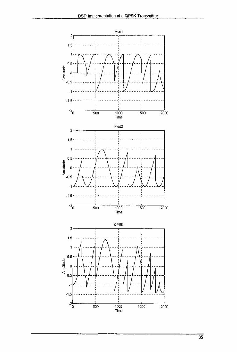
Mod1 2,----~----~
5 ----.-.----- ~---. -·.--.-- ., . -----.----- ., .. ---.-------
05 _\/
0 ••••• v ... -0 5
-1 ---.--.----. ·,· ..... -. ---- ·t •• ··- -- ···- -:--- ••
-1 5 ' ' ' -- ... ------- .,. ---.--------.------------ .,. ------.-----
-2,~----~~--~~----~~--~ 0 500 1000 1500 2000
Ttrne
Mod2 2,,------.------.------.------
1.5 .....•.••••. ., •............ , .......................... .
____________ .. __ .................................... .
' 0.5 ·········----: --------!-------
' ........... ' ' '
-1 ------- ----:-----·--·-· ' r--- ••
-1.5 ' .. ------ .... ., .... ·-- ..... -•...... -........ --.- .. -- ·-.-' '
-2 L__------::'-:--------,~----~~----,-J 0 500 1000 1500 2000
Time
OPSK 2,-----~----~----~----~
1.5 ·········---~---·······--·····---------------------·-
1 ---
0.5 -- - ----- - -- -----
0 -- •• --- ••• -------
-0.5
' '
' ' ' ···-t-- ...... .
-1 ....... --.--:---······· ·!-···-'
·-'--·-··----·· ' ' ' ' -:-- ..
-1.5 --------- ....... - .. -... ·-· ., • ----- .. --· . ., ..... --.- ·- ... .
-2~------::'-:--------,~----~~----,-J 0 500 1000 1500 2000
Time
35
Page 48
5.5.2 Analysis of Simulation Trial1
From the graphs above, by comparing it to the PSK modulation theory, it
seems that all the signals are generated correctly. The signals we are most
concerned about are from Mod1, Mod2 and QPSK.
The graph of Mod1 resulted from multiplying the Quadrature signal with a
sinusoidal wave. We see that the graph Mod1 accurately reflects the
multiplication of these two signals. Where the Quadrature signal is -1, there is
a phase change of 180". This is also true for the In Phase signal. The In
Phase signal is multiplied with a cosinusoidal wave. The graph Mod2 is the
result of the multiplication.
Finally, Mod1 and Mod2 are added, resulting in the QPSK waveform. Again,
by comparing the graphs and adding Mod1 and Mod2, we see that the QPSK
graph is also accurate.
We shall continue with the simulation trials.
36
Page 49
DSP Implementation of a QPSK Transmitter
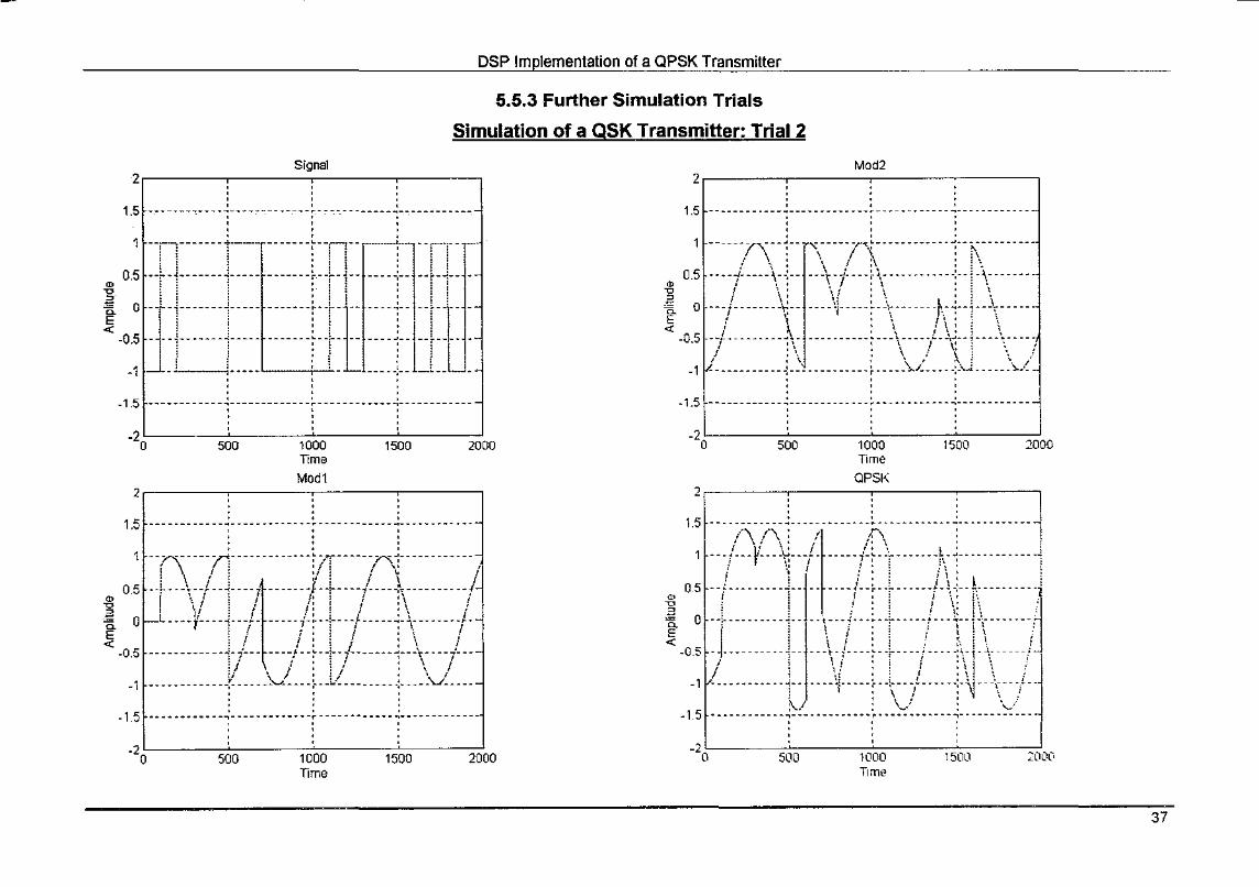
5.5.3 Further Simulation Trials
Simulation of a QSK Transmitter: Trial 2
Signal 2,-----~----~----~-----,
1.5 --- ----~--- -~-------- -----~- ---.-- ------~--. ----------
.
Mod2 2,-----~----~----~----,
1.5 --------.-- -~- -----------------.------- ~------------
.
. 0: :p:::::::r_-__ :::::::::n:: -~-J-ru:: 1_0: tr:::::t::: ::::::::Jr~:: :::::::~~:Ul-:
------l\ --r- '\- --~l\------ ------ T- ~~,-- ---- -----.-/----\-.:.- . --\- i---- ~ \· .. -.---- .. -~--1-\·- ..... -
I \ : ', , , , ' ---r-------~-- .... \)-----~-~\\·-- -r-:+-1--~------
0.5 • ~ -~ 0 ~
E
~ I
]_1 !_____ : ; : : -1 L---+-' -'-'- -----:-- -'--'-
-1.5 ------------~-------------~------------~------------. . -2L------~--~~--~~-~
0 500 1000 1500 2000 Time
Mod1 2,-------~--------.
1.5 --------"""" ~-"""" -------------- .. """"" ~--"--" ------
-1
-0.5
1 ---'\--- -- r-------- -----: /T- --- --"'\'------ ------ .
J-- ~- j_- j_""- ~ -" ---" .t .l.- .. ,{""" ~~"-"""""- -- j 0.5 . ' ' . ' {. . • ' I ·, I i ! .: i I : I f
\I : • I • : I , \ ,
L r : ' I' : / ' • ' ····r-···t···t· ···--r~··t····, ·····-:·"\·-·····-r· • I . f ' \ I : , I , ; I , \ : -- · · · ------ ··r r· · · · ··.f · ·:· T" r·---- ·:-· ·r · · · r · · :I / · 1 • · , I :; ' I ' : I ' ' ; .. ______ . ___ -~-. ____ v_ .. -~- .1./ ..... ___ . -:-. __ .v .....
0
-1.5 . . .
·····-···---~------···----~----·······-~---------····
-2~--~--~~--~~-~-0 500 1000 1500 2000 Time
«
• ~ 3
'@-«
-0.5
-1
-1.5
__ j--- -----. ~'- .. --- ..... ~ ... \.- .. .!.. ~j__.---- ... ---.j :\ \ / 't \ \ /
~.- --- ... -- .. : -~-- ... -.. -.. r-.- . . \...~: ... --~.,J----. _\,./
. . . ------------~--------------------------~------------
-2!----~-----:-::~--=~-~-0 500 1000 1500 2000
T1me
QPSI\ 2,---------------,
1.5
-1
------------------------.--.----------- ----------- --l l\1'\; I l\ : . , . ,. , . I t· \ . '
---;---v---~---i- :·::J:t:r·::::l\1;:::::: ::1 -----------T : ' : ! '' :, l
o -+--- ---- · ·i· · · · r--~·-- -~----- ---;-- -1-- i-\- ------- · I . . ' . . ' . ' -1-------- --i-- ---\-1----r- -r-- --~: __ -- -\-i
1
- ~- ----/j I i 1 :· : ! f : ; : ; ----------- "1"" -- --+----~- -~-- i• ... --~-~-- \•• /••
:--... : '-·' : ,,.· ------------~----·········:·········---~------------
-0.5
05
-15
·'ol_ __ ---i,---;i;;;------;~--~ ,;,- 500 1000 1500 .::OOQ
T1me
37
Page 50
ID
I
~ l
DSP Implementation of a QPSK Transmitter
Simulation of a QSK Transmitter: Trial 3
Signal 2,-------------.------r------,
1.5 ----------- ..... ------------ -~--.,-.-- ------ ... .,. ----------
' -------- ··r-··:--1 ------------+-i '
0.5 ------------~-- i : -------- -+- ~--
' ' ' ' '
-----------1
0 ••••••••••• ""l".
:::::::::r[·:: 1 ' i
-0.5 --···-·····-~--
-1 -~--
-1.5 ------------~-------------~------------~------------' '
-2~----~~----~~--~~----~-0 500 1000 1500 2000 Time
Mod1 2,-------------.------.------,
1.5
' '
-0.5
::::::: ::;n :::;-:::::: :~: :~::::::: L :i~::::: I ' I j'''\ ./;I ·-~----!---- ... ---/- ---- \-~-+---\-----~-/--~----~L
; ; • \. i ' • ; i
--f-- -f..--.~- i-- --- ·t- \-+-- --\---- ~L- · ·t --/---; I i! . 1 :\ 1 \ / 1 / _. V ... __ .. -~:. _ ... ~ ___ . ~ .\L _. _ ... v. -:--._.\...I_ .• _.
1
0.5
0
-1
' ' ' ------------~-------------·------------~-------------1.5
" 2o~----~5~0~0------1~0~00~----~1~50~0~----~20'00 Ttme
Mod2 2,-------------.-------------.
1.5 ------------~-------------~------------~------------' ' ' ' ---,,--:--------··r't---- ------- :------- ·:"", /\: ;:\ : j\
o.s .. -- t-- -- \· -:-------- ;---- ~ ·c----------:-------:---- ·. ~ 1 \: . :\ : r i - ! '. { • \ ' ' l : :En. o ---r------ +\:------:-- ---:·-~- ----- -y-:-- --- ;--- ----1 ...... i ' i : \ ;,: ! !
.1; ~
~
I ; ' ' ' ' , ' ' J -0.5 - -.~. ------ .. -:'.---- ·t- ----- ~--- \---- -f-- T,--.- ,•---.----; •\ I . \ ! ,, I ' ' \ I ' ' ' \. '
-11/.-- --------.: . . \..l.----.-- ~-- -- .\../---- -:-'-''- .... -.-.
-1.5 ' ' ------------~-------------~------------~------------
-2'------~~----~~--~~----~ 0- 500 1000 1500 2000 Ttme
OPSK 2,------,------.------r------,
' ' ----------- ·-:· ... - .• --- •• -~---- ••• --.-- -:·--.------. -. ·:t .'\' ' ' . , ....... . . ' ~ ' . .
-------.f----~----------1\-: --.------ ---~-- ... !. .• , ~- I ' . "' ; . . . . '
------1-----1-------- ·-1-i-+\- ------- .; .. --;:~ -- -F-- ·i
1.5
0.5
r i , •·· i ~ ' i I o ---··r·----~------- -;---A----1;---- ---~--------.---- J
-:~-- /------ -i----~~- 1----r\-~-\-- ---- ~- -;~-~ -r ____ I -0.5
I! ;!"i : .. ~ :;, ---,--------~---t- -'-----~- 1 •.• -'~---~--'-...' ........ .
!, i f : : \ :\ ': ' ~ ~;/: v·~·
-1
-15
-2,'--------:'c--------,C.,..-------,C.,..----....,.J 500 1000 \500 .:ooo
Ttme
-
38
Page 51
DSP Implementation of a QPSK Transmitter
Simulation of a QSK Transmitter: Trial 4
Signal 2,-----~------~-----~------.
1.5 ' -------------:------.-------~---.----------.-~----------
' ' ' ' ' ' 1 ------------t--·--r---,--.-·- --r-:--[:-·---l-
• · • i I '
0.5 -----------+------+----~-+---- -+-~-- ------- -J 0 ------------j------+---;+--- +b--------0-~ ---------J::::::r -:--r:::: I:p::::::: -1.5 ' '
-------------.-------------~-------------.------------' '
~~----~~----~~--~~----~-0 500 1000 1500 2000 Time Mod1
2,-----~----~-----r-----,
1.5 ' ' ----------------------------------------.------------' ' ----------r· --- ·7-y·- -~IT----------:-- --·r··---
' j_' \ :' ; : /! { . ' t ! • • ; 0 5 "• • • • •• ·•l• -~- • • • I •• • • ·\ • •/o • -~- • • • • ••• • •:•· •l• t·· • • • •
-~ I i I t': ! /1 : I l ~ o 1----:----;--r·---- t·:--r-7 ----:r ~---A: <( -o 5 __ ,_ ___ f. .... l-
7{ __________ ~--L-/.., .... Jl. ... l .. J.i,.
'I; '"'I'/' l· 11 :il \J: i, -1 - •• -..L ------ --~------------ -~- .ll.. -----~ -:----- Ll.- ---
-15
' ' ' ' ' ------------ .. -------------·-------------.------------' '
-2 ~-----,c:::-------:~----:;:';,;,-------;;;;', 0 500 1000 1500 2000
Time
Mod2 2,-----~------~------~-----.
1.5 ' -------------.-------------·-------------.-------------
------_/\_--~-- \- --~--r~,---"T'\"--- r·------,l'\ , , I \ , , ,
0.5 ----~ --- -\-~-- -- ·\- ·'---- ;.~--- T -- -~ ---:------ -f--- --' .g: I \• \/ :\ I \: : .a i \; \i : '> 1 \ : I ! o ---r-------~-- ----,-----:·-\~-J-----~.-:-··--r··----
-0.5 .. L ........ ~\. ----------~--\ ______ t ___ _j_ _____ _ l ;\ ; I \' I ' ' ' ' . . .
-1 ~ ----------- ~---- --------- ~------------ .;.'-./..--- ------1.5 ' -------------.-------------·-------------.------------
'2o~----~5~0~0------,~o~oo~----~,~50~0~----2~000 Time
OPSK 2,------r------.-----~------.
1.5 ' ' --------------------------·-------------------,'\ : /"\ !"I r':'. ' ; ' ' ' I ' j I' \ 'l ' ------- !--- ~-- -f--- ~.~- --li-~- -]··--I ---- ~--------- -,1'-
) \• I I ' : ; I ' I ,
0.5 ------/---- -i-- ----- __ / __ ~--!-- -/-\---- -L---Ir-·-l-\ -8 I : ; i \ ; l; i 1_
t -0 : ::
1::/:-:_ r _ :: _: :::: :t: :t: t ::\:: !: : 1: t :t::: ~
I i '!\'/(/ _, -T;-------·t· ----------~--~----·\J_!---p·: _____ l -1 5
-2o'--------~~-----,~:-------c-::::------o7. 500 1000 1500 2000
T1me
39
Page 52
DSP Implementation of a QPSK Transmitter
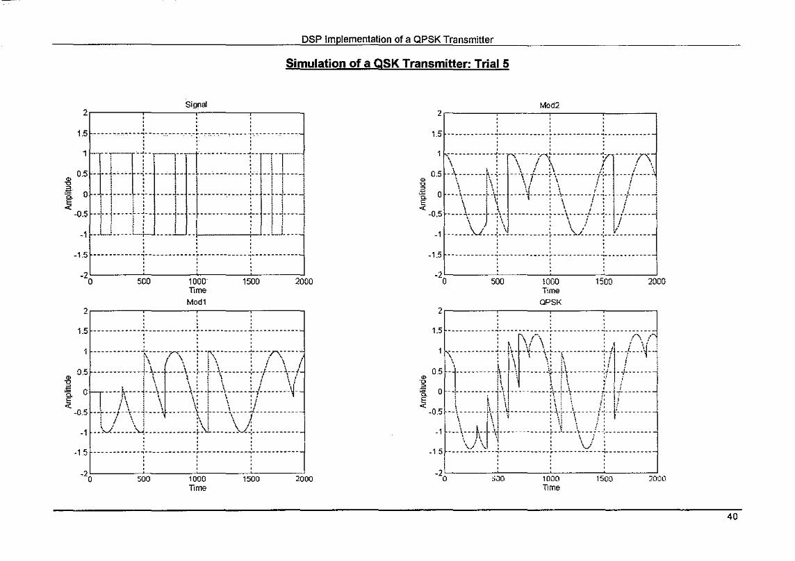
Simulation of a QSK Transmitter: Trial 5
Signal 2,-----,-----~----~-----,
1.5 -------~----~----------------~---.-~-------~-------------
,:~ .1--fr -~l ::::::::::::::: .rr·-~j <l> : ' ' I
~ i : i ! f ~ 0 -j-····, ·j-- ::::r ·········---~-- -+ ~----~
-O~: :H::: :~ -:--____ "- __ .. _-_-_-_-_-_-_-_-_-_-_-_-_·,-_-.1~ ~ ~~~~~I
-1!
t
' ' ' -1.5 ---- --------+ ---- --------~- ----------- ~--------- ----
' '
"2o!:----,5~o::::o---::1o:'::o=oc---,1"5~oo:----oc:!2ooo Time
Mod1 2.-----~------.-----~------.
1.5 ------------~--------------------------~------------
' ' '
0.5
-----------·t ----"T\"-- :- "f'\,- -------:----:0----
----------- -~-\,.--- ----\-- ~- -l--\------ -)-- /---\--/ i ' \ : i \ : ! \{
---- L .. --j- --\- ----- \-~- +-- .\-.---- .!.-/---- ----~-1\ . ' ., • . \ ' ' I \ i \ ,; i I : I
0
-0.5 -+- __ /!.-\--+ ---\ -------\- -[-- ---\---- ~,·!_------- ---: \ ; •\ : \ '
-1 •• 'J. .... I...i ............. f:.J. ...... .J.; ........... .
-1 .5 ' ' -----•••••·-~-----••••••··r···•••••----~----•••••·•-
"2o!:-----c,o~occ----,,~o~o::::o----,~,~o::::o:---~,c;;!o·oo Time
Mod2 2,-----~------~------~-----,
1.5 ' ------------~--------------------------~------------
' ----------- • .J.. ......--- -- ·r-.,t ----------- "':r ----"(\ \ :,;,, I •\
-4--------~-~-- ---\-L--~\-----------1-:-- ----1----\ .g \ i\,: ,/ •\ :: ,.1
' ' ' ' '· ,· : ', ; ' ~ ! 0 ---\-----J' -r.-- ----1-----~--~-------f-.!-- ---j-------1
0.5
-0.5 ____ \_ ____ _l_ ----------~---\----_/_:. ___ /_ ____ _ \ :\ : ' I : l/
-1
-1.5
\ ' \ ' ' ' ' . ------ _J_- -~- ------------}- --- _\..l_--- -:-- -~--------
' ' ' ------------~-------------~------------~------------
' ' ' '
-2,=------~::------c:'::,----:-:':o------::;!, 500 1000 1500 2000
Time
aPSK 2,-----~------.-----~------.
1.5 ----------- -~----- -~- i=-~-- ~-------- ---- ~-- ----"(\ "f
1\ · · · · · ·· · · · i- ·l\ -f.+· v · -~ · · ··· · · · · i-!\-· :1 · · + ; i 0.5-i----- +jl---++\- - -/U -- l I 0 --~-- ------~-1\ ~-- -------+-~-\ ------. /--1:~ ---- ---~
-0.5 --\-------/(j'~----------f\~- \·····ii-f-·······1
_:; :::\Aft: ___ ::::::::'t:: :\/1:::::::::::: -2',-----,~----;~----~-----:o!.
0 J00 1000 1500 2000 T1me
40
Page 53
DSP Implementation of a QPSK Transmitter
Simulation of a QSK Transmitter: Trial 6
Signal 2,-------------~-----.------,
. . ------------~--------------~--------------.------------. . . 1.5
• • . .
! 0 :]::-:[F~::f -· :::::::::_::r _:::r ~-[;- I : ~ : r < ' ' : ' i
-0 s --r---r--i-------1-- ------------1-- -----!--1
--, ,' i ' f
-1 --' ···--:-------..L_ --, :···---L--' . .
-1.5 . . .
------------ .. -------------~-------------.-------------2~----~,---~~----~~--~-
0 500 1000 1500 2000 Time
Mod1 2.-----~-------r------.-------,
1.5
. . .
0.5
------------:--- -- ·r~--- -:- T',- -------:----- r\----· 1 \ · i \ . : \
-- __ . --. _. _. ~- •• -~---- -\- -~- -i-- L -- __ . _ J~-- __ ~--~- ---1l
" '5. 0
' . ' . ' \ j' ' \ :/ \,:!\ \!\ ' I ' : ' : \
1-... L ... ,. .. , . --- ... ,. , . ->-· -1- •. -- -y--, --- -·-
)\ : ( \: ; ~ : \ ; \ ~
-0.5
-1
-1 5
r\ :1 \:' \ :\! \ --:-----·--t---:-~·-----------r--!-----.:...----~---1-r-----"' ' I \ . " ' . I ' ' I __ v _____ ~~--- _________ r:l _____ \.t!. ___ \ _____ _
------------~-------------·------------~------------. . -2~----~----~:;:-------;;~------,~
0 500 1000 1500 2000 1ime
Mod2
0.5
1 : :::::: ;:~: ::: ~~~: ::: :;~(: ::::::::::: :,:~,;:: ::/~J ! t :: \ I 'I !. \ f •• 1 -\ --t-"-- ",, ---- -(-;----: ·. --- ""- ---:-:----I· -+" --1
\ i ! \I : \ ! : ~ I ! 0 ---\1-----' f,------ -~----- ~- -\-------!- +-- --:\ + --- ~
\: ! / • • , I • 1! :
~ it : : \ / : \i --------- -~· --:------------- ~--- \-.-- ..... -- -:------ --;-.--. : : \ / :
------- ----- -!------------ -~---- _\./---- .: .. -----------1
ID ~
,§
~ -0.5
. . . ------------~-------------~------------~-------------1.5
'2oc_ ______ ~5o~oc------c,o~o~o------~,5~oo~----~2~ooo Time
OPSI< 2.-----~------~------~-----.
1.5 --------"-- ,. ----~---:::- ., -- "-------- "'------ -.,_.- 'l : /\(\! f· i~
t . I \: I ' ', ~ I \ ------- \----:-- ·r--- ~--- \:- -~--------- -\-- l\ r\ -l
~ 05 ·1·/++f·--lh ··1--\f~---\J' ~ O -+-- i·-- _\f.- ~-,L--- -------- ~-+ -\------· t--- Jf t- _·_--- \ <( f ! : f : \ ! \ j: \ l \
-o.s --"-~----- -~L------------~-v---\------ 1 ..:- ___ .i:. ______ . \ i j : d \ : : 1 i
---\ L-- .. L-A--- _______ ._-~-L _-\ __ )_) ____________ J \i i :' \ ! 'i ;/ \ \../
------------~-------···---~------------~------------
-1
-1.5
-2~-----,~----:io:----;i;;;---:;;'. 0 500 1000 1500 2000 Ttme
41
Page 54
l ~
-1l 3
~ "'
DSP Implementation of a QPSK Transmitter
Simulation of a QSK Transmitter: Trial 7
Signal 2,-----,-----~----~-----.
1.5 ' ---------~--- .. ·-----.-------~--.,--------- .. ------------'
----------,----:-----l
----------~-~-----'
0.5
-· ·-- r-f------------------i------r -- · ---: : i I ' ' : - -~---- ---------:-- ---~--- --- -l ' ' : :
0 ---------- l --~ ------------ J __ --- ~------ ~ -0.5 --:-----
. ' ' ' i i
--~-------------:-----r------""1
' ' !: i --~-- -----------:-----' '
-1f--------'-~----------' ' ' '
-1.5 ' ' ' ••••••••••---,---------••••r••••---------,----•••••••· ' ' '
'2o~----~5~o7o------1~o~o~0----~1~5o~o~----~2o·oo Time
Mod1 2,-----~------~-----.------,
1 5
' ' ' ---------·r· ----------- -· --------T'-"-----"-· · · ; j : I ~ ~ \
---- -----l- -~--- ·1 ------- ~- ---- --!---- -:;;---- r-- ~ .. --,. i 1 ~~ : ; :1 1 \ I ' ' ' ' : '
----f··--"';---!- ---- \-~------f-----~-\---~----\-1 : f \' ' ' ' : \ ' : I ,, I 1 I : •
--:----/-----+ f··- -- ··f- -\--- -l- ------ ~-- -\- t--- --\ • I '! t " , , , ' ' ; ! ' •\ / ' \! ' __ ~-.L- _____ --.'- _____ v ___ -~v ________ .:. ____ .._ _____ _
05
-0.5
0
-1
' ' ' ······••••·-.,·····•••·····r····••••••··-.·······••••· '
-1.5
-2~----~----~~----~~--~-0 500 1000 1500 2000 Tlme
Mod2 2,-----~------~-----r------,
1.5 ' ------------ .. ·------------~-------------.-------------' ' '
' ' ' ------l\--1-/'\-- --r,~- ---~\---- r---- -------0.5 ----1-- ---t -rr----\-1--- ---1----\---:------ -A----
u_:_ 1 , \· ; \ : !i , - I (. ;{ ' , : /i ; - 0 ---·------ -r-------··----- .. t ....... ,._, •• ----,-1·---. § ! i;: i I \: ; f -.. J l( : I \ : / :
~ l
-o.5 -T- ----- -~ -:------------- j·------ --- -..:;--- ·;· -T--- ~ ' ' ' \ ' \ '
-1 ------------ ~-- ---------- -t-- ---------- -~:.---- Jo....C ' '
-1.5 ' ' ••••••······-.····•···•••••r••··········-.-••••••····· ' '
-2~----~~----~~--~~----~. 0 500 1000 1500 2000
T1me
QPSK 2,------r------~-----.------,
1.5
-- ·ltk/l·---]1\-- --/\"--···6---------j ti-r ----.-1·· -----;'------,·:·----r--1
f·--/ ; ; i ! ! : ! '
o ----- J.- -- ~- J.L- -t--- J_-- --- -i--- ---- L--- L .t. ••. 1 ! I 1 ; l . l ; \ I i 1 i I .I •• j \
---- }__---- --'(-----~- .!. --- - --t-------- A----'--- .L --
·1 I : \/ I I l \ ! \ ! --: f-------- ~----- --1----- r· ~/--- ------- -:- \" -- r----\- ·i
!/ ' ! ' \ ; ; i • : ,._/ :, ... 'J ------------ .. -------------,------------ .. ------------
05
-0.5
-1
-1.5
-2:-------ic:------;;;';;~----,.,~--~ 0 500 1000 1500 2000
Tune
42
Page 55
DSP Implementation of a QPSK Transmitter
Simulation of a QSK Transmitter: Trial 8
Signal 2,------r----~~-----.------.
1.5 -··· ----------:- ---···- ---- -·- ----- ···---. -:--------.---' ' '
0: ~!-:::::::~.; .. :: .f .. l ... ::::::: ---- :J ~ ' ' ' i -~ I 0 - ! mmr·· t ::.t:::: ::::::: .
-0.5 ·-r·------ -T- -r- I : --- - _--.1 -1 -: _,__ .L --~L ... '--+-'·······
-1.5 ' ' ' ' ' ------------.. -------------·------------~------------
' ' ' ' ' ' '
-2\--------,:;S' ,------:;;\;;;-----;-;';;;;-----;;;;, 0 500 1000 1500 2000
Time Mod1
2,------.------~-----.------,
1.5 ... -------- -~- ---- ------. -~- ... ----.--- ~-- ---.-----.
' ' 1 ------·--·r··---T,----:·--·---·····:·---:,------. , I , . . ,,
f ' ' ' ' ' ' ~ o_
5 -------7 --y·--r·---\·r------~-~-----\--.rr----:-" 0 n---.,----;--·1·· ....... ,., ...... ! ----,-r--r--··1!' E 1 ' • ' •; · , __. ' i J " I ' I i ! I --.. ; ' ' I• I . ., ' : ' .o.5 --r--·;----·;;----·----··t----,--,----~1·----r·-;-·,-,1: :\:V.' ;/\
-1 --~J .. -.-. --~- ___ .... --- __ ~.\../ _. _. __ .. ;. ----Ll ....
-1_5
' ' ' '
------------~-------------·------------~--------··--' ' ' '
'2o,L-------:,~ooc------c,of.o~oc-----~1~5~ooc-----~,cCoo·o T1me
Mod2 2,-----,-----~----,------,
15 ·: ::: ;~:: :;:::: ::::: ::~T ::: :~~;:::: ;:; :::: ::_: j-\ , \ :/] / ~. i \ l ! / \
0_5 --\.-/..- -- -l-- ~~ -~----- ..:. ---;.;-.- i-.- )~- -1-:-- i----!----1'l B ~ 0
\I 1.!! / :\l \/:!I I ---1-- ---~' i~- -1-- --r--- -~--~- 1!- --- -v- ~-- l -- r- ---l ---------- !_ L.l.- .,L ... --~---\ ~-----.- ~-- ! . ./.- ----- -i "" -0 5
: i : : \ : : I i
.1 .......... ~LL ···+···: ...... :.f ....... l -1 5 ------------1·------------r·-----------1·-----------"l
·'o,L----:,.c~o""'---.,.10":'o"o----:1-eSo"oc----:,c"ooo Time
QPSI\ 2,------,-------,------~-----,
05
15 .... '"/ • ""i\'; : . ~- :· ... 'l • • \ ' ': ' I' I I
\-----.rTr:~~ -·:---r·-\r- ---- /r--- rn· -.-----. .!Yl \ I ·, ' '• · ' •I ' • --:----1·-- - - -.~---r----- -~~- -·- -~-1---- ·,•- , .. ,,. --!-- 1 -~
% B '5. 0 ·t··F'·/i·F--·+·H· IH·:L \j
--'·~----·-- 1·'·/----·--·''1···•·--+•··--•--•·•·--·J t ! i : ' I l : : l i / I \ : i j ; i \1 I ; ' i I
-1 -·-' -·--·- --:--jl-------- -~. -\·- ;---- -{--:----- ~/--- --- ~
.... ' ....... 1..~-------···~--\J ....... ;. .... · ...... ~ L_ ____ ~: ----~~: ~--~~'~--~~. ~20-- 500 1000 1500 20JO
.1' -0.5
-1 5
Time
43
Page 56
DSP Implementation of a QPSK Transmitter
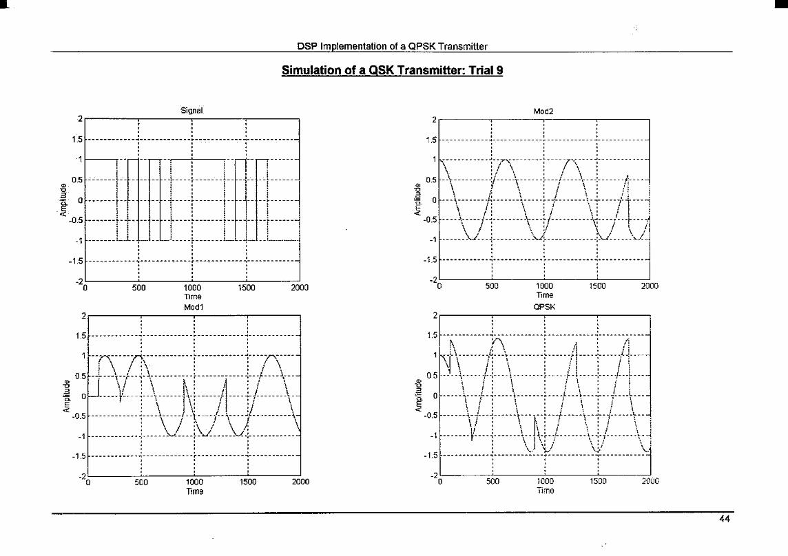
Simulation of a QSK Transmitter: Trial 9
Signal 2r-----,-----~-----,-----,
1.5 . ------------i·------------~------------~------------
1 f-------,, -T •-- -,----+----,. --n--, ---------1·----}-------t-- -+- --~------!
0.5 -------1---
~ !
1_0: ::::::11: -j---+------1-- _]I ____ [_ ____ _
-1 J:::::::::::t : -~ :t:~~ ' .
-1.5 . . . ------------~-------------~------------~------------. . . . .
-2o!c-----5~o"'o----:-1o~o:::o---.,15'"'o"o---c2=:'ooo nme Mod1
2,-----,------,----~-----.
1.5 . ' ------------~-------------~------------~------------. . . . . . .
1 --n--- --n- ------------ ,_ ----------- ,_- --~'-- ---' \ I :\ : : I \ ' t ' 1 ' . ' 1
i 0: ~LV-:L\~~~~~~~j\;::::::;1-::::v::::\ < ' " ' '! '
-0.5 ------------ i· -- -\·--;-·\ --~{-\-- ·J. ---------"\ -1 ------------ _;_ ---- _\...1 __ --~ v-- -- .J.:.-- ---------. . . ' . . . .
------------~-------------~------------~------------. -1.5
-2!:-o----5~o':;o:----:-1of-o:::a:---:;15';;o;;-o----:2::!oo·o nme
~ 'i5_
)[
.g ! <
Mod2 2,-----~-------.------~-----, . . .
1.5 ---------- --;- ---------- __ ,------ ------ ;-- -----------. . ' . . . . 1 ['\---- --------:- - ... -.;:--- -----~----~--~ ---- -:-------------"I ·I~,\' ' ' \ ' ' ' .
o.s -~- ------- -~/---- -\----- -~---!----),.-- .:. ------A----\ : \ : I \ : /~ i
0 ' I' \ ' l , ' ' • : ---\------- -r:----- '\----- ~- T------- \- -:·---- T T' --- i
-0.5
\ I • ' • , I • 1 : \ t: \ :1 \: l- ~
---- -\:' --;·:· ------- '\- -:;- --------- \:'"- ·;-- t---}
-1 -----\J.-- ~-- --------:J;. ----------- .\..t~-- __ \/ -1.5
. . . ••••••••••··~··••••••••-••e-----·······~··•••••••••• . . . . .
-20 L ------,1-,-----~',-,-____ _,:~ ____ ,l 500 1000 1500 2000
Time QPSK
2.------.------.------.-------
1.5 ----------- -~------ -------------------- ~-- ----------' "'\ ' ' .. " ~ ' ~ ' ,, __ L \ _______ L _ .\ _________ ~- ____ _fl ____ _: _____ .LJ. __ _
1\J I } : I ' ! ! : j [
o 5 -~- .\ .. --- -l~--- .\ -------- r---- j j ---- -!----J _ _l_ ---! i : \ : i \ : .i !
o ---- .L-.1. ~- --- .\.----- -~--- -f ---\--- ~--- )_- .. L---( I • 1 • \ • .' I
1 r • • • ; 1 • r I -0.5
. ' I ' ' ' ' ' ' ' '
---- --~~-;- -~----- -\--- 1-· + --f- ----\--+-r- ---\-- i !,1 ' 1 I ' I I • i \ :
-1 ------- t---- ~- ------ ·-- -1-r- -i---- --- -•- -H---- --- ·t-....; : \ l \: / \ :/ \ ' -· ~ ~ ~ -1.5
. ------------~-------------~------------~------------
_,L_ ____ ~ ______ _L ______ ~ ____ _,J
0 500 1000 1500 20UO Trme
•
44
Page 57
~
}l
l -<
DSP Implementation of a QPSK Transmitter
Simulation of a QSK Transmitter: Trial10
Signal
r ' 1.': ~,--------- -~- -------- -~- 0 -~- ------------ ~..,----- ------
1
0 0
----------- --+-· . .
____________ j __ 0.5
0 ------------~--I ' ; I ! ,-----:·rr·· ----1 ......... ___ '
-r----·rt
8j------- -------- ---~
-0.5 ---------- --l~ -11-----------i
:r:::r:r :::::::r:::::::::i -. . . - ,------------ .
0
-1.5 0 0 •
·-----------..,-·•••·······•r••••••••····-.···••••••·--o 0 0
-2~----~----~~----~~--~-0 500 1000 1500 2000 lime Mod1
2,-----~------~----~------.
1.5 ----------- -~- ----------.--- ·---------- .... ------.----
-1.5 . . ••••••• • ••- ·~- ·-- ........ ·r·--· ··•• • •• • ., •.. -· .... ·-·
'2o~----~5~0~0------~10~0~0----~1~5~00~----~20ooo lime
~ u g ~
~
Mod2 2,-----~------.------r-----,
1.5
. .
0.5
----"I\--:----.----T''------ ------ "i"· .. -- '7\-
--- -I----\\-~-------- f-- -\-------- --1--l .. -/----\' 1 ' ' ' \ ' • ' . I I: ! : \ I ; ,' i 0 ---. ------- -~------ -1---- -~- -\--------;- ... -- -- "r ----- . .., ! ~ ! :\ !; J • _I _______ ... \ ____ I .... _~ __ -\ ____ .L _ ~-- _ ,r_ ______ _
/ :\ / : \ / : I ! ___ --------.\. v ___ ----- ~-- --\.i __ -- -':-- -~------ --
-0.5
-1
-1.5 • • 0
···•••••····-.···•·•••••···r····••••••••-.·•·········• 0 0
-2L-----~~--~~----~~----~ 0 500 1000 1500 2000
Time QPSK
1.: --- ------- --~-------- ----- ~----- ------ j__----------J /\: t-.1'\ t n ' ' ' ' ': \ ' ' : ' '' ' '. ' ' .. -----f----\-:-------;-- t~·-r--------- ·\··------,!--,
I' ~ ! I ; i l f i i / I ; i i 1 / i 0.5 ------ J ----- ~-----·I-. --1- ·r-- +--.-----. i--.----- -,--- ..
i I \ } : l : I .!
!_0 : ~~::;-·::::r:::t:::::::r: ::,::· r::J:: ::t::: -1 --~ ! ...... --~---t. ---- ... -~--L .. . !; .. /. _: __ ~---·~-- ___ .
; I : I ' \ ! : ' ' I ' =! ' I ' , ;. ;\. ,\_,·v',\/
------------ .. ··-----------~------------ .. -------------1 5 0
-2'----~~----~~--~~--~-o- 500 1000 150D 1000 T1me
45
Page 58
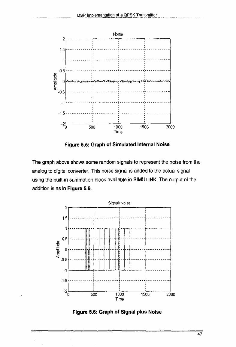
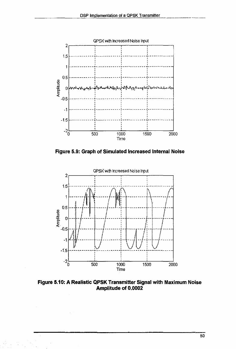
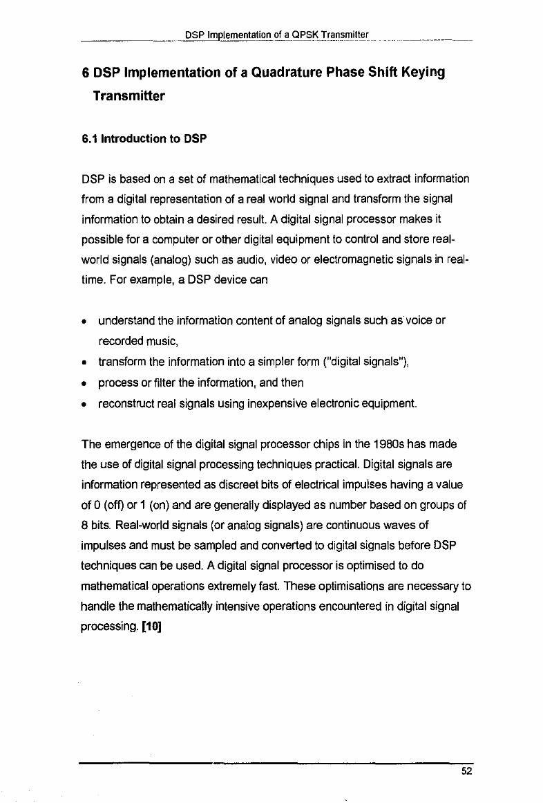
5.5.4 Simulation of a Non-Ideal QPSK Transmitter
The simulations above were for an ideal QPSK transmitter. It was deemed
ideal as there were no considerations for internal (thermal) noise that is
present within all physical components. To implement this noise into our
simulation, we include a noise generator to our SIMULINK QPSK transmitter
diagram. SIMULINK has a built-in block that enables us to include noise to our
original transmitter diagram.
Figure 5.4 shows the amended diagram for our simulation with noise.
R;,rd~rn S:gnal i}~r,;.;.;ttlr
·8 S:gnal
SineW Jve S1neScope +
Timing Adder
Timin~ Genera or
Switch1 In Phase
BPSK Mod2 BPSk_Scope
8 Cos1na W<ife
CosmeScope
Figure 5.4: Amended SIMULINK Diagram with Noise consideration.
In the diagram above, white noise is added to the signal. By doing this, we are
assuming that the noise is coming from the analog to digital converter.
However, this block can be included anywhere on the diagram (since all
physical components emit internal noise), although the amplitude of the noise
is extremely small.
We examine the graphs after simulation.
46
CJ
QPSK Signal
Page 59
"' "0
" 1
2'r----,---- -------,---
"1 .5 ------------ ~-----. ------ .; ----- ------ --·-- -----.-------' '
' ' ------------.J·------------·------------~-------------' ' ' '
' 0 5 --- ----------:-----------.- ~--------- ----:------.-----' ' ' ' ' ' ' ' ' 0 ,...,..r._.~-~~f'>l"'--""·.l'l..~·.h;j!o.1...,_"\J''-'.....,., :-..-',J':.w:o~·~ .. ._,.._,,....:, ' ' '
-0.5 ' ' ' ' ' • • • •• • • •• •• • .J •• ·• • • • • • • • • • L • •• • • • • • •• • • •'· • • • • • • • • • • • •
' ' ' ' ' --1 --- -· --------:------------- r -------------:-------------
, '
-1 5 ' ' ----.------ ..... ------.----.----------- . .,. --------- .. -' '
-2.'------::!-::---:-:'':-:----------:-:':c:-------= 0 500 1000 1500 2000
Time
Figure 5.5: Graph of Simulated Internal Noise
The graph above shows some random signals Ia represent the noise from the
analog to digital converter. This noise signal is added to the actual signal
using the built-in summation block available in SIMULINK. The output of the
addition is as in Figure 5.6.
Signai+Noise 2.------.-------r------~------
' ' ' 1.5 ----------- -~-- -----------:------------ ·:- -----------
' ' ' ' 1 -------- -,- i- --,- ---., : ___ , ________ ,_______ . . I ' . . .
! I j I .: l ~ ~
~ 0.5 --------:-:- -- --r-----~ 1----1--------l-------------i ';::! ! : r,!l :i /
1
1 ! "' 0 -------- - - ·- - ---" ·----1----------------------l § !t it: i t I - li ! i: i i i
-0.5. -----·-- . ---; :!··--1--------:-------------i il '' I I I
-11-------'--"---j 11 l I ) i
-'------'~
' ' -1.5 ------------ ~---- ----- ---- ~ ------------ .: .... ---------
' ' ' ' ' ' ' ' ' ' ' ' '2.'------;!:::-------;:!;:-;:--------:c:':-:----::: 0 500 1 000 1500 2000
Time
Figure 5.6: Graph of Signal plus Noise
47
Page 60
The noise cannot be noticed in the graph above as the amplitude of the noise
is too small. However, when the signal is processed by SIMULINK, we can
see a difference in the resultant QPSK signal. We compare the two QPSK
signals below. The first graph (Figure 5. 7) is from a simulation that does not
have noise, in other words, an ideal transmitter. The second graph (Figure
5.8) is from a simulation that has noise included. We can see that the noise
has an effect on the QPSK signal.
5.5.5 Analysis of the Non-Ideal QPSK Transmitter Simulation
From this simulation, we observe that to achieve an effective QPSK
transmitter, it will be necessary then to eliminate noise that has a high enough
amplitude to affect the transmitted signal. Noise that has small amplitudes
might not affect the QPSK signal significantly, as simulated above.
As with all communications systems. our objective is to obtain a suitable
signal to noise ratio, SNR, and a low bit error rate, BER. From our simulation,
we see that when the noise amplitude is set to 0.0001, there is some
evidence of signal corruption. This corruption (the BER) increases when the
noise amplitude is increased to 0.0002, as can be seen in Figure 5.10 below.
The QPSK detector I receiver must be able to detect the presence of noise
that has been transmitted and eliminate it from the signal before processing.
One method this can be achieved is by using a bandpass filter, to filter other
frequencies other than the carrier frequency. A filter can also be included in
the transmitter itself to stop noise frequencies that is other than allowed by the
filter. However, it is obvious that this will not stop noise that has frequencies
that is in the range of the filter and carrier frequency.
48
Page 61
QPSK W1th No Noise Input 2,-----,------r----~------,
1 5 ---------- --~------- --- ---·- -------- ----!---··----- ---·
(\i /l f:\ \ / ------- ·1--- .,~. ----- -· .... J .... ------------ ~--- -----~--
1 ·~ i !I! \ I 0.5 ------ J--- --~----- ./ .. _j_ -~-- ---.-.------i------t-.-
ID
~ 0 a.
, ' I ' i I I i ! i r
-----1------~-----/-------:------------ --1-----i----/ i r : 1: i I !i
-0.5 r ; J , 1, : r Tl------+-- -;--- --- -[-- ----T -t+- f--- -1-----
-1 __ _;__ ____ .L--1---------l-- ___ ;L_f-LL-11------
!j !/ •\J!/!!, 'v . , , . ) , , .\.. : :V : \. ~.... : I .. -- ... -· ... ., .. ---·. -- • •• ·r· -· -·. -· ...• .,. ••• •• .. • .. ---1.5
' ' ' ' ' '
-2 ':-------:-::-:-----c::':-::------:-:=:-----:::! 0 500 1000 1500 2000
T1me
Figure 5.7: An Ideal QPSK Transmitter Signal
OPSK With No1se Input 2.----.---~---.---,
1.5 ------------ ~- ------------ ~------- ------:-------------
~n ; 'i- f\ '\ ,. 1 ::::::;n:~ :::::::!: t1;:_\ ::::::::::l:r::::!:-
1 °: -----11------ -----!------;-- ---------1H----~i----0.5 ---r----- ----;--------;-- ----~1---, rr-,-----1 -- ·--------~---J---------r-\1·-J --h-t;--1-------
v :,.J;\. -1.5 ------------,-------------~------------~------------'
-2!:------:-!::--------:-:':::---------;-:!:c:-------:::!. 0 500 1000 1500 2000
lime
Figure 5.8: A Realistic QPSK Transmitter Signal with Maximum Noise Amplitude of 0.0001
49
Page 62
0
i E
""
DSP Implementation of a OPSK Transmitter
CPSK with Increased Noise Input 2.-----~------.------.------,
1,5 -- --· -··- ---~------···· -· -- ·---· -· -- -· --~-----. -- -· ---' ' ' ' ' ' ' ' 1 ----------- -~--- --------- -~- ------. -----:-------------' ' ' ' ' ' ' ' ' 0_5 -------------:------------- t- ------------:-------------' ' ' ' ' ' ' ' '
0 ~"'"'""''>-~"-~lt-... .,fl'f ... ,'l.t'-><'t'-',1'<•"'-">.Jo'"'-"" ' ' ' ' ' ' '
·•••• • •• •• • • -'· •· • • • • • ·• •• • L ••• • • •• • • ·• ·•'•• •• • • • • • •• ••
' ' ' -0.5 '
-1 -------------:------------ -r ----- ·------ -:------------' ' ' ' ' ' ' -1.5 ' ' '
------------~-------------·------------~-----------· ' ' ' ' ' ' ' -2 '----::-::----:-:'::":----:-::':'::----:-:'
0 500 1000 1500 2000 Time
Figure 5.9: Graph of Simulated Increased Internal Noise
QPSK with Increased Noise Input 2.----r---~---.---,
1.5 -- -- ··-.-- ----.----··-.-- -· -- ~- --.-.-- ---- .,. --------.--' : /l~f\ !\ ( 1 -------~1- -{-----1-- ' !.: --------)\------·i·
~ I ' . I i i !' I o.s --+-- --- - ------F-- --r-- ---------+-1---·--t--Q) r: I I ' ! i I i o -+!------ -----1-------f-- ---------H----r--"" -OS Jr·---- ---r·-·-·-r-- -··r-IH-·I---
-l --~~-------- ·-r----·---i-- --nJ-:--u----· -fs -------------- ~- ------- -.--- -~ --------- -- --:-- ---- -·-----
' ' ' ' ' ' ' ' ' ' -2 '----=-:-----:-:':7---:-::':-:----:::'. 0 500 1000 1500 2000
Time
Figure 5.10: A Realistic QPSK Transmitter Signal with Maximum Noise Amplitude of 0.0002
50
Page 63
As a comparison, we include a graph of a QPSK signal with a maximum noise
8mplitude of 0.01, an increase in the noise of a factor of 100. From the graph
(Figure 5. 11 ), we observe that the signal has a high BER, and the original
QPSK signal is nearly unrecognisable.
OPS!< with Increased No1se Input 2.------.-------r------.------,
1.5
0.5
I . : ----•-i '
' --- - i-
' ' . ' -1.5 f-- ___ _-_ -- ___ ; __ -----------:-------- ---- ,_ -------c_ --~
' ' ' ' . -2 L--------::-C:------~:-------:-:':--:----~
0 500 1000 1500 2000 lime
Figure 5.11: A Realistic QPSK Transmitter Signal with Maximum Noise
Amplitude of 0.01
5.5.6 Conclusion
From the above simulations of a non-ideal QPSK transmitter, we conclude
that noise has a detrimental effect on our generated QPSK signal. However, if
the noise amplitude is small, the degradation of the signal may not be
significant. In other words, the QPSK decoder I receiver may be able to ignore
the small corruption and be able to decode the signal.
The MATLAB code is included in Appendix C, for further investigation.
51
Page 64
------
6 DSP Implementation of a Quadrature Phase Shift Keying
Transmitter
6.1 Introduction to DSP
DSP is based on a set of mathematical techniques used to extract information
from a digital representation of a real world signal and transform the signal
information to obtain a desired result. A digital signal processor makes it
possible for a computer or other digital equipment to control and store real
world signals (analog) such as audio, video or electromagnetic signals in real
time. For example, a DSP device can
• understand the information content of analog signals such as voice or
recorded music,
• transform the information into a simpler form ("digital signals"),
• process or filter the information, and then
• reconstruct real signals using inexpensive electronic equipment.
The emergence of the digital signal processor chips in the 1980s has made
the use of digital signal processing techniques practical. Digital signals are
information represented as discreet bits of electrical impulses having a value
of 0 (off) or 1 (on) and are generally displayed as number based on groups of
8 bits. Real-world signals (or analog signals) are continuous waves of
impulses and must be sampled and converted to digital signals before DSP
techniques can be used. A digital signal processor is optimised to do
mathematical operations extremely fast. These optimisations are necessary to
handle the mathematically intensive operations encountered in digital signal
processing. [10]
52
Page 65
...
DSP Implementation of a QPSK Transmitter
6.2 Introduction to the TMS320C542 DSP board
The TMS320C54x has a high degree of operational flexibility and speed. It
combines an advanced modified Harvard architecture, a CPU with
application-specific hardware logic, on-chip memory, on-chip peripherals, and
a highly specialised instruction set. [11]
The '542 DSP board has 2k of program ROM space and 1 Ok of Dual Access
RAM (DARAM).
Standard 1 ta" mini-jacks for direct microphone and mu~imedia speaker
Voice quality 'AC01 DSP external
address bus Socketed 22V 1 0 PAL for HPI applications
connection r--:,.~ .. ~, .. -;~~~~~~~"""'\!~~~~~~~ ...... m~~~r-"":"!~":::----, ~:9)
Universal· 5Y poV>/er supply included
Buffered Serial Port (BSP) and Host Port Interface (HPI) control signals
XDS510 emulator port (IEEE1140 .1 standard)
DSP external data bus
8 bit bidirectional , 4 bit unidirectional printer port connectivity, enabling high speed applications
Figure 6.1: The Texas Instruments TMS320c542 DSP board
Some of the key features of the '54x DSP are
• Advanced multi-bus architecture with one program bus, three data buses
and four address buses.
• · 40 bit arithmetic log.ic unit.
53
Page 66
---------'D""S,.,P_,I~Iemen!ation of a QPSK Transmitter-------------~-~------------
• Two address generators, including eight auxiliary registers and two
auxiliary register arithmetic units.
• 192k words x 16 bit addressable memory space.
• Instructions with a 32 bit long operand.
• Arithmetic instructions with parallel store and parallel load
• Conditional store instructions
• Fast return from interrupts
• Programmable timer (11]
6.3 Implementation Considerations
There were several methods considered to implement a QPSK transmitter.
These methods deal with generating BPSK signals initially. The reason, as
described in the PSK theory, is that QPSK is just an extension of BPSK.
6.3.1 Method One
The first method that was considered was to sample and store a sinusoidal
wave into one half of the on-board memory of the '542 DSP board. A polar
NRZ digital wave is then sampled and stored in the other half of the memory
space. Finally the two sampled waveforms are multiplied to form a BPSK
wave before being channelled out to a digital oscilloscope. It is obvious that
this method does not allow for 'real time' signal processing.
A program code for the '542 board was written to sample and "record" a signal
that is passed into the board. This code was modified to suit our needs in
regards to memory allocation for the sampled data. This program saves a
total of approximately 0.45 seconds of input signal. In other words, two copies
of the same program were actually used except for the different codes to
specify different memory allocations.
54
Page 67
According to the Texas Instruments TMS320C54x DSKP/us DSP Starter Kit
manual on page 1-5, lhe useable memory allocalion is belween 0080h and
27ffh (where h represents the hexadecimal format) in the data memory map
section. However, when a sinusoidal signal was recorded belween the
memory locations of 0080h and 027ffh, and when the signal was played back,
the result seen on the oscilloscope was a random signal for some
milliseconds before the sinusoidal signal was observed. This is obviously an
error, as the signal that was played back should have been a smooth
sinusoidal signal. It was initially contemplated that the input signal could
possibly be distorted at the start of the recording.
To overcome this problem, we examined all possible memory locations where
there is no distortion to the recorded signal. It was found then that the memory
addresses between OOfOOh and 027ffh were the range that was free from
distortion.
To test this method again, we divided the new memory location into two equal
sizes. One copy of the program with memory allocated between OOfOOh and
01 b80h was loaded into the '542 board and a sinusoidal signal from a function
generator was channelled in. Next, the other copy of the program (see
Appendices D and E) with different memory allocation codes (between
01b81h and 27ffh) was loaded into the board, and the same sinusoidal signal
was channelled. When the signal is played back, the signal from the first
allocated memory location (OOfOOh to 01b80h) is slower than the original
signal that was channelled into the board. In other words, the period of the
sampled signal is approximately twice the original signal, but the amplitude is
halved. This is not the case with the signal that is stored in the second
memory allocation, however. This second signal was almost identical to the
input signal, except for a negligible reduction in the amplitude due to the
sampling.
The reason for this particular anomaly is not as yet known, as there is no
apparent reason as to why this is occurring since the codes of these two
programs are identical except for the memory allocation codes.
55
Page 68
i
Due to the fact that this method does not allow for 'real time' signal processing
as well as the anomaly in the sample and record program, it was decided to
implement another method.
6.3.2 Method Two
This second method that was considered was to sample a sinusoidal
waveform and save the data on to the on-board memory of the '542 DSP
board. The next step H1en is to pass through a non-return to zero (NRZ) polar
wave that represents a digital information stream into the board and modulate
it with the sampled sinusoidal wave. The output is then a BPSK waveform.
Again, this procedure does not enable us to process the digital signal in real
time. As mentioned above, the sinusoidal signal is only 0.45 second in length
due to memory restrictions, so when the digital signal is passed into the DSP
board, only 0.45 second of the information signal is converted into BPSK.
6.3.3 Method Three
A third method is to actually generate a sinusoidal signal via DSP code and
multiply it with a NRZ digital signal to produce the required BPSK signal. This
method was the one selected as the favoured of the three methods described
above, as it is not only logical to implement this method, but also it will create
BPSK signals in real-time. [It shall be noted here that 'real-time' is not actually
immediate, but the processing of the digital signal within the DSP board does
take several milliseconds, but it is negligible in our circumstances.]
56
Page 69
_____ _,D~SecP_.,IrD.P.Iementation of a QPSK Tra~_~f!IJtle~-------··- ____________________ _
6.4 DSP Code
The DSP code to generate a BPSK signal is adapted from a sample program
that is available with the '542 DSP board. The sample code was to generate
an AM modulation signal from an analog signal that is channelled into the
board via the input socket. Necessary modifications were made to the
program code to acquire our BPSK signal, but the main program structure
was observed.
The PSK modulation code like most programming languages today are object
oriented. In object oriented programming, the overall program is made up of
lots of different self-contained components, each of which has a specific role
in the program and all of which can talk to each other in predefined ways.
The BPSK code has several functions called by the main program. There are
actually two programs, psk1.asm and psk2.asm. These two programs have
almost the same functions except that psk1.asm has a 2 kilohertz sinusoidal
wave as a carrier and psk2.asm has a 2 kilohertz cosinusoidal wave as a
carrier. As these two programs are almost similar, we only need to examine
one of these codes. A full explanation of the codes will be examined in section
6. 7 and section 6.8.
The code for the DSP board was written and tested using a single +5 voltage
signal. [The DSP code is included in ihe Appendix F for further perusal.] The
output on the oscilloscope was a sinusoidal signal, which is what we require.
When the voltage signal was removed, there is no signal seen on the
oscilloscope. This is confirmation that our code is working as expected.
6.5 Filtering
We include some filtering with our program. We expect that FIR filtering
should elim1nate some noise from our input (assuming that our signal has
noise included). We now examine the FIR filter and filters in general.
57
Page 70
DSP Implementation of a QPSK Tran~!!JJI!er __ ... ________ ·-------------
FIR filters are usually implemented using structures with no feedback (non
recursive structures). Digital finite impulse response filters are discrete time
invariant systems in which an output number, representing a sample of the
filtered signal, is obtained by weighted summation of a finite set of input
numbers, representing samples of the signal to be filtered. The coefficients of
the weighted summation constitute the impulse response of the filter and only
a finite number of them take non-zero values. This filter is of the finite memory
type; that is, it determines its output as a function of input data of limited age
[15].
With advances in VLSI, digital signal processors are now available to
implement digital filters in real time. An analog filter operates on continuous
signals and is typically realised with discrete devices. A digital filter operates
on discrete-time signals and can be implemented with a digital signal
processor [14].
Different techniques are available for the design of FIR filters and the most
common utilises the Fourier series. In designing such filters, we use
N
y(n) = '[.h(k)x(n-k) k=O
If the input is the unit pulse x(n) = 0(0), the output response will be the impulse
response y(n) = h(n).
This equation also shows that an FIR filter can be implemented with
knowledge of the input x(n) at time n and of the delayed inputs x(n-k).
A useful feature of the FIR filter is that it can guarantee linear phase, where all
the input sinusoidal components are delayed by the same amount (14].
58
Page 71
-------""DS,P_,Ime..-P,.-Ie'"m"'en-'"ta,..,ti"'one_:of a Qf_S~_Trar:!_~r!ll.~~~! ____________________________ _
6.6 Window Functions
In order to obtain a realisable FIR filter, the infinite series in the transfer
function equation
Hd(v) = 00
" C e i""" '-'" n=-oo
was truncated, yielding a finite number of coefficients.
[Note that Cn are the Fourier series coefficients, vis an introduced normalised
frequency variable, where
FN is the Nyquist frequency, or FN = Fs I 2. The sampling period, T = 1 I Fs.]
This is equivalent to multiplying the filter's coefficients by a rectangular
window function with amplitude of 1 between -Q and +Q, and 0 elsewhere.
The rectangular window function is defined as
Wn(n) = {l,[n[ < Q
0, othenvise
An FIR filter with the rectangular window function has high sidelobes caused
by the abrupt truncation.
In our DSP code, we use an 80 tap FIR filter to implement a bandpass filter,
The filter passes frequencies between 200 Hz and 1.8 KHz. Blackman filter
windowing was used when calculating the filter's coefficients [14].
59
Page 72
____ DS~~.elementation C!f a QPSK._!ra_~_s.D':IJ!!~! .. ~ .. - _________________ _
The Blackman window function is
{0.42 + 0.5cos(mr I QJ -t- 0.08cos(2mr I W.lnl ~ {2
Wu(n) = O,otherwise
The Blackman window provides the largest reduction in sidelobe ccmpared to
other window functions, it has the widest main lobe. However, the width of the
main lobe can be reduced by increasing the width of the window via the
number of coefficients.
The coefficients can be calculated using MATLAB. MATLAB has a command
that will calculate window functions such as Boxcar, Hanning, Bartlett,
Blackman, Kaiser and Chebwin. By default FIR1 uses a Hamming window.
Other available windows, can be specified with an optional trailing argument.
For example,
B = FIR1 (N,Wn,bartlett(N+1)) uses a Bartlett window.
B = FIR1(N,Wn,'high',chebwin(N+1,R)) uses a Chebyshev window.
6. 7 DSP Code Description
The main program [see Appendix F] ccnsists of three different parts or
phases. The first phase initialises the DSP board. The main program makes
calls to psk_ac01.asm and psk_vecs.asm and coeff.asm, where the
psk_ac01.asm file initialises the Analog Interlace Circuit. The psk_vecs.asm
file contains the interrupt vector table. The sub-program coeff.asm was initially
used for a bandpass filter. As mentioned previously, the coefficients of the
bandpass filter was calculated using Blackman filter windowing.
60
Page 73
DSP Implementation of a QPSK Transmitter _________ _
In the second phase, we generate a carrier frequency. The difference
equation used for the generation of the carrier is
y(n) = A'y(n-1) + B'y(n-2)
Depending on the coefficients of A and B, we can generate different
frequencies of the carrier signal. In the main program, the frequency is
determined by the coeff, sinx and Yminus1 variables. In our case, we
generate a carrier frequency of 2 kilohertz by giving coeff a value of
678[dec.], sinx a value of 15531 [dec.] and Yminus1 a value of 02bf[hex.]
The final phase multiplies the carrier with the digital signal input and sends the
PSK modulated signal to the transmit register.
6. 7.1 First Phase
We examine the first phase of the main program, which is the initialisation of
the DSP. We first look at the psk_ac01.asm sub-program.
Certain AC01 registers can be initialised by using a conditional assembly
constant. By setting the constant REGISTER to the appropriate value the
assembler will either include initialisation for certain registers or ignore
register initialisation. The constant REGISTER can be set to include the
following AC01 register:
REGISTER (binary) =
0000 0000 0000 0001 -> initialise Register 1 (A Register) 0000 0000 0000 0010 -> initialise Register 2 (B Register) 0000 0000 0000 0100 -> initialise Register 3 (A' Register) 0000 0000 0000 1000 ->initialise Register 4 (Amplifier Gain-Select) 0000 0000 0001 0000 -> initialise Register 5 (Analog Configuration) 0000 0000 0010 0000 ->initialise Register 6 (Digital Configuration) 0000 0000 0100 0000 ->initialise Register 7 (Frame-Sync Delay) 0000 0000 1 000 0000 -> initialise Register 8 (Frame-Sync number)
61
Page 74
Any combination of registers can be initialised by adding the binary
number to the REGISTER constant. For example to initialise Registers 4
and 5, REGISTER= 18h. Upon assembly, only code for register 4 & 5
initialisation is included in the AC011NIT module. When called the
module will load the REG4 and REGS values into internal AC01 registers.
Register 4 is always loaded to get a 6db input gain. This sets full-scale
to 3v(p-p input) due to the single-ended AC01 configuration. [13]
The initialisation program can be viewed in Appendix H. It shows the step by
step line code of the program and has description of each step.
We now investigate the psk_vecs.asm program. This sub-program initialises
the vector table for the main program. The vectors in this table can be
configured for processing external and internal software interrupts. The
DSKplus debugger uses four interrupt vectors. These are RESET, TRAP2,
INT2, and HPIINT. These four vectors were not modified as the debugger will
not work properly if done so. All other locations were free to be used. (A list of
interrupt locations and priority table is available in Appendix 8 of the Texas
Instruments TMS320C54x DSP Algebraic Instruction Set Volume 3). The
vector table code is found in Appendix I.
As mentioned above, the coeff.asm sub-program is not initially needed in the
testing of the program. However, it is useful in the elimination of noise by
narrowing down the range of which noise can occur. We realise that noise can
occur at any frequency, bui if we allow only a certain frequency through and
limit our intelligent signal to that frequency, then we can stop all other noise
frequencies from being transmitted as well. The bandpass filtering can be
implemented at a later stage, with only minor modifications needed to the
main program. The coeff.asm sub-program is listed in Appendix J with
description.
62
Page 75
_______ O<D,SP'-"'Im"'p"'le"'m""en"'la,li,Q!l_Qfi!_ QPSK Trans~itt~_r -·---·-·------------------------
6. 7.2 S&cond Phase
This second phase involves the generation of the carrier frequency. A
sinusoidal signal was generated using the difference equation
y(n) = A'y(n-1) + B'y(n-2).
L y(n) " /
' / ' ' /
A 1/Z
'~ X y(n-1)
/
B 1/Z
X y(n-2)
Figure 6.5: Ftealisation of the Differential Equation y(n) = A'y(n·1) + B'y(n-2).
This is computed in the main program.
63
Page 76
DSP Implementation of a QPSK Trans!Tlilte.r:_ ______ ·~-~---
6.7.3 Third Phase
The final phase involves the multiplication of the carrier with the input and
sends the PSK modulated signal to the transmit register. Again this phase is
implemented in the main program.
6.8 Description of the psk1_main.asrn Code
In this section, we analyse the psk1_main.asm code step by step. The full
program code is available in Appendix F.
* FILE NAME: PSK 1 MAlN.ASM
.title "BPSK Modulation"
.width 80
.length 55
.mmregs
These few lines give the introduction to the program, presenting the title of the
program and the initialisation of the display page .
. setsect ".data", Ox400, 1
.setsect ".text", Ox1800, 0
.setsect 11Vectors", Ox180, 0
.setsect 11filter", Ox2700, 0
These four lines of .setsect initialises the sections of memory to be allocated
for data, text, vectors and filter .
. sect "filter"
.copy 11Coeff.asm 11
The .sect command assembles the coeff.asm data (which is copied using the
copy command) onto the filter section.
vector table .sect "vectors 11
.copy 11psk_vecs.asm"
64
Page 77
DSP Implementation of a Of'SK T~!!.~_r:Dl!!.~-----~---------~------
This is similar to the above procedure, where the data from the psk_vecs.asm
file is copied and assembled onto the vectors section. The line ;vector table is
just a comment.
.data
sim: .word 15531 : 31061 Yminusl .word 02bth , XN .word O,O,O,O,O,O,O,O,O,O ; 80 data locations for 80 XN I .word O,O,O,O,O,O,O,O,O,O stage delay line. XN2 .word 0,0,0,0,0,0,0,0,0,0 XN3 .word O,O,O,O,O,O,O,O,O,O XN4 .word 0,0,0,0,0,0,0,0,0,0 XN5 .word 0,0,0,0,0,0,0,0,0,0 XN6 .word 0,0,0,0,0,0,0,0,0,0 XN7 .word 0,0,0,0,0,0,0,0,0 XNLAST .word 0 OUTPUT .word 0
' ; extra word for the bit bucket
This section is the data section. Yminus1 and sinx are variables and the size
of these variables are declared (using the command . word) with the values. (A
word length is 32-bit.)The memory space for 80 data locations is also
declared with an extra word for the bit bucket.
.text
start: intm = I call ACOIINIT pmst = #0 I aOh sp = #Offah DP=#O imr=#240h intm = 0 nop
WAIT: goto WAIT
receive: DP = #XN
; globally disable all interrupts
; set up iptr ; set up init stack pointer
; set up RINT and HPJ !NT ; turn on all interrupts
; wait for receive interrupt.
; This sets Data Memory Page Pointer to page XN, which is defined
; earlier in the program.
65
Page 78
This is the text section of the program. This part sets up the pointers used in
the program. intm is a bit in status register ST1 (status register 1) that globally
masks or enables all interrupts. As described above, setting intm to 1 disables
all interrupts. A call is then made to AC011NIT, which is found in the
psk_ac01.asm sub-program. pmst (processor mode status register) is a 16-
bit register that controls the memory configuration of the device. The data
page pointer (DP) is set to 0. The DP is a 9-bit field in STO that specifies
which of the 512 128-word pages is currently selected for direct address
generation. The imr is a 16-bit memory-mapped register used to enable or
disable external and internal interrupts. A binary 1 written to any imr bit
position enables the corresponding interrupt (when intm = 0).
;--------generate carrier ----A=#O A= @Yminusl « 16 ; y(n-2) >ACCUMULATOR A SHIFT
; LEFT BY 16 BITS! (Q31 format) A= -A ; -y(n-2) =>A macp(@sinx,coeff,A) ; (coeff)*y(n-1)- y(n-2) ==>A macd(@sinx,coeff,A) ; 2*(coeff)*y(n- I)- y(n-2) ==>A @sinx = hi( A) « 0 ; Store the carrier generated into
; variable sinx.
This section is where the carrier frequency is generated. First we initialise the
accumulator A to 0. Next we send the value of yminus1 to the accumulator
and shift it left by 16 bits. We then negate the value in the accumulator. The
macp instruction multiplies a single data-memory value (@sinx) by a program
memory value (coeff), adds the product to A (the accumulator) and stores the
result in A. The macd instruction is similar to the macp instruction except that
the data-memory value (@sinx) is copied into T (the temporary register) and
into the next address following the @sinx address, while the macp instruction
copies the data-memory value into T only.
The next command stores the carrier generated into the variable sinx.
66
Page 79
------"'D"S,_P_,Im,_,pocle"m"'e=ntation of a QPSK Tran~mil_!~!_
A~ lrcv ; Load ACC with word from AIC
@XN ~ A « 0 ; Store the value of received ; word to variable XN
ARO ~ #XNLAST ; Load ARO with address ofthe last ; delay element!
@OUTPUT~ A ; Store the input into ; variable OUTPUT.
A= #0 ; Accumulator A initialise to zero.
repeat(#79) ; Repeat next instructions 80 times. macd(* ARO-,hO,A) ; Compute FIR output. @OUTPUT~ hi( A)« 0 ; Store the filtered input into
; variable OUTPUT. A~ #0 ; Zero Accumulator A.
The command trcv (Time Division Multiplexing data receive register) is a
register used to receive data through the TDM serial port. In this command
line, we load the accumulator A with the data from the Analog Interface Circuit
(AIC). The symbol @ represents the direct addressing mode. The symbol#
represents the immediate addressing mode.
·----------PSK modulate on carrier '
macp(@OUTPUT,sinx,A)
@OUTPUT~ hi( A)« 0
A~ @OUTPUT « 0 A~ #OFFFCh & A tdxr~ A return enable
transmit: return enable
; Multiply the carrier with the ; output.
; Store the PSK modulated signal ; into variable OUTPUT. ; OUTPUT ~~>Accumulator A
; Send to transmit register ; Enable interrupts and return ; from interrupt.
; Enable intenupts and return ; from interrupt.
; ----------------------- end ISR -----------------------------
.copy "psk acO 1 .asm 11
.end
67
Page 80
------~D=~!:lf!!plementation of a QPSK_ T!!~§!!!!!~~----- --------·-·--- _____ _
In this final section, we modulate the carrier with the signal. First, we multiply
the carrier with the output, then store the modulated signal into the variable
OUTPUT and copy the data from OUTPUT into accumulator A. Finally, we
send the signal to the tdxr, the TOM data transmit register. This register is a
16-bit register used to transmit data through the TOM serial port.
6.9 DSP Hardware Implementation
To actually implement a QPSK transmitter, we actually require two separate
OSP boards, since there is only input and one output per board. We require
two inputs (for two NRZ signals) and two outputs, which are two BPSK
signals. These two signals are then added to produce the QPSK signal. (At
this stage we are not yet looking into generating a single NRZ signal and
separating this signal into two different data streams.)
The next step was to find a source of NRZ signals to see if the DSP code is
processing the digital data properly. A teaching board, the Lab-Volt: Computer
Interface Base Unit and the Digital Communications 2 boards were used to
generate random NRZ digital signals. This particular board has several NRZ
signal output points in which we shall extract the signal from.
A DSP board was loaded with the one of the PSK codes and the NRZ signal
from the Digital Communications board was channelled into it. The output
from the board is connected to a digital oscilloscope. (A digital oscilloscope
was chosen because of its ability to store and hold data). The code was
executed, and the output signal observed on the oscilloscope was very
favourable, and in accordance to the BPSK signal generation theory. This
result was equivalent with the second OSP board.
68
Page 81
l
DSP Implementation of a QPSK Transmitter
Figure 6.2: The Lab-Volt Digital Communications 2 Board
Since we were able to generate two BPSK signals we require a signal adder
to generate a full QPSK signal. For this part, we shall use a simple operational
amplifier. The operational amplifier we have chosen to use is the UA 7 41 CP
Op-Amp from Texas Instruments. The design for the adder is illustrated
below. We note that the signal that is produced by the operational amplifier is
inverted. As this is the case, we need to invert the signal to get the original
QPSK signal. This is easily done with another operational amplifier connected
to the first op-amp. The output from this second op-amp will be the QPSK
signal. Figure 6.3 below shows the simple signal adder using the UA741CP
Op-Amp. As indicated above, the signal is inverted. Figure 6.4 shows the
solution to correct the signal inversion.
69
Page 82
DSP Implementation of a QPSK Transmitter
R3
Signal1 R1
a!k +
Signal 2 ___~,VR2\f\r---'------'---i .rok
R4
Ground
<: 01(
Signal o'utput
(Inverted)
Figure 6.3: Signal Adder for QPSK generation
Signal1 ZOk ~------.
Signal 2 20k Wv- --'----'----1
20k
I i
;o-1 Ok
Ground _
Figure 6.4: Corrected QPSK Signal Output
Signal Output
(Corrected)
70
Page 83
DSP Implementation of a QPSK Transmitter
Figure 6.5: Actual UA741CP Operational Amplifiers
Connected as in Figure 6.4
Figure 6.6: The Laboratory Setup of the DSP QPSK Transmitter
71
Page 84
DSP Implementation of a OPSK Transmitter
Figure 6.7: Enhanced Photograph of Digital Oscilloscopes Displaying
Digital Signals and QPSK Waveform
The final design was combined with the output signals from the two DSP
boards and the output from the operational amplifier was connected to a
digital oscilloscope. A second digital oscilloscope with two channels (and an
add function) was atta.ched to the output to the two DSP boards. By doing
this, we can easily compare the output of the operational amplifier to the
added output signals of the DSP boards. Figure 6. 7 shows the digital
oscilloscopes' displays. The bottom oscilloscope has the real - time DSP
generated QPSK waveform.
When the two signals were displayed on the oscilloscopes, it was observed
that there is a slight delay from the output signal of the operational amplifier
compared to the one from the two added output signals.
72
Page 85
7 Conclusions and Further Development
7.1 Conclusion of the Thesis
The aim of this project was to develop a DSP implementation of a QPSK
transmitter. This transmitter was to process digital signals in real-time and
modulate it with sinusoidal and cosinusoidal signals to produce the required
QPSK wave. This objective has been achieved firstly via simulations using
MATLAB's SIMULINK package and finally using the Texas Instruments
TMS320C542 DSP processors.
The simulation and DSP implementation results were confirmed by comparing
it with the theory of PSK modulation, showing that the SIMULINK design as
well as the DSP code is correct. The DSP code was further improved by the
implementation of a low pass digital filter calculated using the Blackman
windowing. This low pass filter has a window between 200 Hertz and 1800
Hertz, allowing a signal within these frequencies to be modulated with the
carrier frequency. Any noise outside this window will not be modulated. The
obvious drawback is that any noise that is within the window will be modulated
and transmitted along with the digital signal.
7.2 Further Considerations and Development
One suggestion is to use another version of a DSP processor. One
consideration is to use the TMS320C3x DSP processor. This processor
enables the use of fioating point processing.
Another DSP board that would be suitable for the implementation is the
TMS320C8x. This board is one of the fastest processors available. It is a
single chip, parallel processor that can be used for applications such as image
processing and audio/video digital compression. The processing power of the
73
I
Page 86
--------'D""S~P~Im=plementation of a QP§_K T!ansmitt~r _______ ... ------·- ·-·--·-- __ _
'C80 also supports applications within the digital telecom, security and image
recognition markets [12].
Five powerful fully programmable processors and a sophisticated Direct
Memory Access controller with CRAM, SRAM and VRAM interface are all
integrated onto a single \C. Applications that require a large amount of
processing can be then implemented with the 'c80. Also all five processors
can be programmed in assembly language as well as in C.
This DSP implementation can be simply carried out by converting the
SIMUL\NK code to C and then downloading the algorithms onto the DSP
board.
7.3 Areas of Further Investigation
Numerical analyses of the DSP implementation of the transmitter are still yet
to be investigated. The efficiency [in the sense of signal to noise ratio (SNR)
and the bit error rate (BER)] need to be taken into account in the construction
of an effective QPSK transmitter.
Another area that is recommended for further development is the DSP code
itself. The current code is still to be examined for any unknown bugs and may
be modified to be more 'stream-lined', concise and efficient.
74
Page 87
_ DSP lm~lementation of a QPSK 1L~nsr!.@er ··-------
Significant References
[1] Halsall, F. (1995). Data Communications, Computer Networks and Open
Systems (41" ed). England: Addison-Wesley.
[2] Sklar, B. (1988). Digital Communications Fundamentals and Applications.
Englewood Cliffs, New Jersey: Prentice-Hall.
[3] Haykin, S. (1983). Communication Systems. (2n' ed). New York: John
Wiley and Sons.
[4] Haykin, S. (1989). An Introduction To Analog and Digital Communications
New York: John Wiley and Sons.
[5] Anonymous. (Dec 1993). SIMUL/NK Users Guide. The Mathworks Inc.:
Natick.
[6] Proakis, J. G. (1995). Digital Communications. (3'' ed). Englewood Cliffs,
New Jersey: Prentice Hall.
[7] Couch, L. W. (1997). Digital and Analog Communication Systems (51" ed).
New Jersey: Prentice Hall.
[8] Stremler, F. G. (1990). Introduction to Communication Systems (3'' ed).
Massachusetts: Addison-Wesley.
[9] Carlson, A. B. (1986). Communication Systems: An Introduction to Signals
and Noise in Electrical Communication (3'' ed). New York: McGraw-Hill.
[10] Price, R. (1995). What Is DSP? [on-line]. Available WWW:
http://www.dspwatch.comlpage1.htm
75
Page 88
[11] Texas Instruments Reference Set Volume 1. (1996). TMS32DC54x DSP
Handbook. Owensville, Missouri: Texas Instruments.
[12] Texas Instruments (May 1996). Chapter 1: Overview of the TMS320C80
[on-line]. Available 'NVWV: http://www.ti.coml .. ./320c80x/oview.html
[13] AC011nitialisation Routine [Computer Software] (Jul1996) Dallas, Texas:
Texas Instruments.
[14] Chassaing, R (1992) Digital Signal Processing with C and the
TMS320C30. New York, John Wiley and Sons.
[15J Bellanger, M. (1989) Digital Processing of Signals, theory and practice (2" edition). New York: John Wiley & Sons
76
Page 89
DSP Implementation of a QPSK Transmitter
Appendix A: A MATLAB SIMULINK Simulation of an Ideal
BPSK Transmitter
bpsk.m
function [ret,xO,str,ts,xts]=bpsk(t,x,u,flag); 'bBPSK is the M-file description of the SIM!JLINK system named BPSK. % The block-diagram can be displayed by typing: BPSK. ~
~ SYS=BPSK(T,X,U,FLAG) returns depending on ~LAG certain % system values given time point, T, current state vector, X, % and input vector, U. % FLAG is used to indicate the type of output to be returned in SYS.
% Setting FLAG=l causes BPSK to return state derivatives, FLAG=2 % discrete states, FLAG=3 system outputs and FLAG=4 next sample ~ time. For more information and other options see SFUNC. % % Calling BPSK with a FLAG of zero: % [SIZES]=BPSK([], [], [],0), returns a vector, SIZES, which % contains the sizes of the state vector and other parameters, % SIZES(l) number of states % SIZES(2) number of discrete states % SIZES(3) number of outputs % SIZES(4) number of inputs % SIZES(5) number of roots (currently unsupported) % SIZES(6) direct feedthrough flag % SIZES(7) number of sample times
' % For the definition of other parameters in SIZES, see SFUNC. ~ See also, TRIM, LINMOD, LINSIM, EULER, RK23, RK~5, ADAMS, GEAR.
% Note: % %
This M-file is only used for saving graphical information; after the model is loaded into memory an internal model representation is used.
% the system will take on the name of this mfile: sys = mfilename; new_system(sys) simver ( 1. 3) if ( 0 == (nargin + nargout))
end;
set_param(sys, 'Location', [441,197,975,647]) open_system(sys)
set_param(sys, 'algorithm', 'RK-45') set_prram(sys,'Start time', '0.0') set_F.aram(sys, 'Stop time', '20') set_param(sys,'Min step size', '.01') set_param(sys, 'Max step size', '.05') set_param(sys, 'Relative error', 'le-3') set _par am { sys, 'Return vars', ' ' )
add block ('built-in/To Workspace', [ sys, 'I', 'To Workspace' ] ) set:Param([sys, '/','To Workspace'], ...
'mat-name', 'Output', .•. 'position', [355, 122,405, 138])
77
Page 90
DSP lmfiementation of a QPSK Transmitter
add_ block ( 'built~ ir· i Signal Generator', [sys, '/', ['Signal',l3, 'Generator']]) set_param( [sys, 'I', ['Signal' 1 13, 'Gt:'!nerator' ]] , ...
'Peak','l.OOOOOO',, .. 'Peak Range','5.000000', ... 'Freq','l.OOOOOO', ... 'Freq Range','l0.000000', ... 'Wave', 'Sqr', .. . 'Units' , 'Rads', .. . 'position', [105,333,150,367))
add block('built-in/Product',[sys,'/','BPSK mod']) set:Yaram([sys,'/','BPSK_mod'],... -
'position', [230,203,260,227])
add block('built-in/Sine Wave', [sys, '/','Cosine Wave']) se(~param( [sys, 'I', 'Cosine Wave'], ...
'phase', 'pi/2', ... 'position', ( 115,195, 145, 225])
add block( 'built-in/To Workspace', [sys, 'I', 'To Workspace!']) set:=param( [ sys, 'I', 'To Workspace!'), ...
'mat-name','Cosine', ... 'position', [205,107,255,123))
add block ('built-in/Scope', [sys, 'I', 'Cosine Scope' J) setJaram{ [sys, 'I', 'Cosine Scope'], ...
'Vgain', '2.000000', .. . 'Hgain', '20. 000000', .. . 'Vmax', '4.000000', ,,. 'Hmax', '40.000000', ... 'Window', [ 65, 63,396, 377] 1 •• ,
'position',(455,35,485,65))
add block('built-in/Scope', [sys,'/','BPSK Scope')) set=param{[sys,'l', 'BPSK Scope'), .. .
'Vgain', '2.000000', .. . 'Hgain', '20.000000', •.. 0VmaX 1
1 1 4,000000 1
1 , , ,
'Hmax', '40.000000',, .. 'Window' 1 i 68,512,393, 707], ... 'position', [465,200,490,230])
add block{'built-in/Scope', [sys, '/','Signal Scope']) set Jar am ( [ sys 1 'I', 'Signal Scope' ] 1 •••
'Vgain', '2.000000', .•. 'Hgain', '20. 000000', .. . 'Vmax', '4.000000', .. . 'Hrnax' r '40. 000000',,., 'Window' 1 [65, 203,396, 517), .•. 'position', [475,315 1 505,345])
add block('built-iniTo Workspace', [sys, '/','To Work~pace2']) setJaram([sys, 'I', 'To Workspace2'],,,,
'mat-name','Signal', •.• 'position' ,[315,277,365,293])
add_line(sys,[150,210;225,210]) add_line(sys,[265,215;460,215]) add_line(sys,[155,350;180,350;180,220;225,220]) add_line(sys,[180,330;470,330]) add_line (sys, [170,210; 170,50;450, 50])
78
Page 91
DSP Implementation of a QPSK Tral}smitt~~---------------------
add _line (sys, [295, 215; 295, 130; 350, 130]) add _line (sys, [ 170, llS; 200, 115]) add_line(sys, [180,285;31.0,285])
drawnow
'6 Return any arguments. if (nargin I nargout)
¥. Must use feval here tc.. access system in memory if (nargin > 3)
if (flag == 0) eval([' [ret,xO,str,ts,xts]=',sys,' (t,x,u,flag); '])
else eval( ['ret ,, , sys,' (t,x,u,flag); '])
end else
{ret,xO,str,ts,xts] = feval(sys); end
else drawnow r, Flash up the model and execute load callback
end
79
Page 92
________ __,o,s,P_c:lm"'p"le._,m.,e._.n,.,l,.,at,.,io~n ~f ~-QPSK Transmit!er ---------·----~~-·
Appendix B: A MATLAB SIMULINK Simulation of an Ideal
QPSK Transmitter
qpsk.m
function [ret,xO,str,ts,xts]~gpsk(t,x,u,flag);
~QPSK is the M-file description of the SIMULINK system named QPSK. % The block-diagram can be displayed by typing: QPSK.
' % SYS=QPSK(T,X,U,FLAG) returns depending on FLAG certain % system values given time point, T, current state vector, X, '!l and input vector, U. % FLAG is used to indicate the type of output to be returned in SYS.
' % Setting FLAG=! causes QPSK to return state derivatives, FLAG=2 % discrete states, FLAG=3 system outputs and FLAG=4 next sample % time. For more information and other options see SFUNC.
' % Calling QPSK with a FLAG of zero: % [SIZES]=QPSK{[],[),[],O), returns a vector, SIZES, which % contains the sizes of the state vector and other parameters. % SIZES(1) number of states % SIZES{2) number of discrete states % SIZES(3) number of outputs % SIZES(4) number of inputs % SIZES(5) number of roots (currently unsupported) % SIZES(6) direct feedthrough flag % SIZES(7) number of sample times % % For the definition of other parameters in SIZES, see SFUNC. % See also, TRIM, LINMOD, LINSIM, EULER, RK23, RK45, ADAMS, GEAR.
% Note: This M-file is only used for saving graphical information; % after the model is loaded into memory an internal model % representation is used.
% the system will take on the name of this mfile: sys = mfilename; new_system(sys) simver(1.3) if (0 == (nargin + nargout))
end;
set_param(sys, 'Location', [391,42,997,539]) open_system(sys)
set_param(sys, 'algorithm', 1 RK-45') set_param(sys,'Start time', '0.0') set_param(sys,'Stop time', '20') set_param(sys,'Min step size', '.01') set_param(sys,'Max step size', '.05') set_param(sys,'Relative error', 'le-3') set _param ( sys, 'Return vars 1 , 1 1 )
add_block('built-in/Sum', [sys,'/', 'Sum']) set_param([sys, '/','Sum'], ...
'position', [435,160,455,180))
add block('built-in/Product', [sys, '/', 'BPSK modl']) - -
80
Page 93
DSP Implementation of a QPSK Transmitter
set param([sys, '/', 'BPSK modl'], ... - 'position•,(345,113 1 375,137])
add_block ('built-in/Scope', [sys 1 'I',' Sine Scope']) set_param([sys,'/','Sine Scope'], .. .
'Vgain', '2.000000', .. . 'Hgain', '20.000000', .. . 'Vmax', '4. 000000' 1 •••
'Hmax', '40.000000', ..• 'Window', [350 1 -4, 675 1 182] 1 •••
'position', [ 475,25, 500, 55])
add_block('built-in/Scope', [sys 1 '/','Sine Scope1'1l set_param( [sys 1 'I' 1 'Sine Scope!' 1,.,.
'Vgain', '2.000000' 1 •••
'Hgain' 1 '20. 000000' , .. . 'Vmax', '4. 000000', .. . 'Hmax', '40.000000 1
, •••
'Window', [350 1 178, 67 5, 373], ... 'position', [450, 285,475, 315] l
add _block ( 1 built- in/Scope' , [ sys, 'I 1 , 'Sine Scope2' ] ) set_param([sys,'/','Sine Scope2'],,,.
'Vgain', '2.000000', ..• 'Hgain','20.000000', .. . 'Vmax', '4.000000', .. . 'Hmax', '40. 000000', .. , 'Window', [350,371,675 1 566], .. , 'position',[530,250,555,2801)
add block('built-in/Signal Gen;;rator', [sys, 'I', ['Signal', 13, 'Generator']]) set _par am ( [ sys, 'I', [ 1 Signal' , 13, 'Generator' 1 ] , ...
'Peak', '1.000000', •o o 'Peak Range','S.OOOOOO', ... 'Freq', '1.000000', .. o 'Freq Range', '5.000000', ... 'Wave', 'Sqr',.o. 'Units', 'Rads', o. o 'position',[30,103,75,137])
add block('built-in/Sine Wave', [sys,'/', 'Cosine Wave']) setJaram([sys,'/','Cosine Wave'], ...
'phase', 'pil2', ... 'position', [165,157,180,173])
add block('built-in/Product', [sys, 'I','BPSK mod2']l setJaram ( [ sys, 'I 1
1 'BPSK..:.. mod2'] , o , . -'position',(345,373,375,3971)
add block('built-iniSignal Generator', [sys, '/', ['Signal',13,'Generatorl'Jll set_param([sys, '/', ['Signal',13, 'Generator!']], ...
'Peak', '1.000000', o.o 'Peak Range','5.000000' 1 •••
'Freq', '1. 000000 1, •••
'Freq Range','5.000000', .•. 'Wave', 'Sqr', .. . 'Units', 'Rads', .. . 'position',[40,363,85,397])
81
Page 94
DSP Implementation of a QPSK Transmitter ~·~--~-·----·---·-·
add block ( 1 built-in/Sine Wave 1, [ sys, 'I 1
, 1 Sine Wave 1 I)
set=param{[sys,'/ 1 ,'Sine ~iave'], ... 'position', [ 165,415,185, 435])
add_line{sys, [90, 380;340, 380]) add _line {sys, [ 80, 120; 34 0, 120)) add_l.ine(sys, [380, 125;400, 125;400, 165;430, 165]) add_line(sys, [380, 385;395, 385;395, 175;430, 175)) add_line (sys, [460, 170;495, 170;495, 265;525, 265)) add_line(sys, [185, 165;310, 165;310, 130;340, 130)) add_line ( sys, [ 190, 425; 315, 425; 315, 390; 34 0, 390]) add_line (sys, [390, 125; 390,40; 470, 40]) add_line (sys, [395, 245; 4 35, 245; 445, 300])
drawnow
% Return any arguments. if (nargin I nargout)
else
end
% Must use feval here to access system in memory if (nargin > 3)
if (flag == 0) eval ( [ 1 [ret, xO, str, ts, xts) = 1
, sys, 1 ( t, x, u, flag) ; 1
] )
else eval(( 1 ret =', sys,'(t,x,u,flag); 1
])
end else
[ret,xO,str,ts,xts] = feval(sys); end
drawnow % Flash up the model and execute load callback
82
Page 95
DSP lmplement~tion of a QPSK Transf!!.i_!!~f -----------··-··----·---
Appendix C: A MATLAB SIMULINK Simulation of a Non-Ideal QPSK Transmitter
modqpsk.m
!unction [ ret.xO.str,ts,xts]~modqpsk(t,x,u,flag); %MODQPSK is theM-file description of the SIMULINK system named MODQPSK. % The block-diagram can be displayed by typing: MODQPSK. % % SYS~MODQPSK(T,X,U,FLAG) returns depending on FLAG certain % system values given time point, T, current state vector, X, % and input vector, U. % FLAG is used to indicate the type of output to be returned in SYS. % % Setting FLAG~ I causes MODQPSK to return state derivatives, FLAG~Z % discrete states, FLAG~J system outputs and FLAG~4 next sample % time. For more information and other options see SFUNC. % % Calling MODQPSK with a FLAG of zero: % [SJZES]~MODQPSK([],[],[],O), returns a vector, SIZES, which % contains the sizes of the state vector and other parameters. % SIZES( I) number of states % SIZES(Z) number of discrete states % SIZES(J) number of outputs % SIZES(4) number of inputs % SIZES(5) number of roots (currently unsupported) % SIZES(6) direct feedthrough flag % SIZES(7) number of sample times % % For the definition of other parameters in SIZES, see SFUNC. % See also, TRIM, LINMOD, LINSIM, EULER, RK23, RK45, ADAMS. GEAR.
%Note: This M-file is only used for saving graphical information; % afte1 the model is loaded into memory an internal model % representation is used.
%the system will take on the name of this mfile: sys = mfilename; new_ system(sys) simver(l.J) if (0 = (nargin + nargout))
set__param(sys,'Location',[683,96,960,582]) open _system( sys)
end; set__pararn(sys,'algorithm', 'RK -45') set__param(sys,'Start time', '0.0') set__param(sys,'Stop time', '20') set__pararn(sys,'Min step size', '0.05')
83
Page 96
______ _,D_,SP,_I~plementation of a QPSK Transmjtte_r -~---- -----··---·
set _param(sys,'Max step size', '.0 I') set_pararn(sys,'Relative error','l e-3') set __ pararn(sys,'Return vars', 11
)
set _param( sys, 'AssignSampleTi meColors', 'on');
add_ b lock('bu i It-in/Sum', [ s y s, '/','Sum']) set _param([ sys,'f,'Sum'], ...
'position',[125,80, 145, I 00])
% Subsystem 'Sign'.
new_ system([ sys, '/','Sign']) set_param([sys,'/','Sign'],'Location',[ 159,4 I 7,467,586])
add_ block('built-in/Outport', [ sys, '/','Sign/out _I']) set_param([sys, '/','Sign/out_!'], ...
'position' ,[265, 70,28 5, 90])
add_ block('built-inllnport', [ sys, '/','Sign/in _I']) set_param([sys,'/','Sign!in _I'], ...
'position',[3 5,3 0,55,50])
add_ block('built-in/Relational Operator',[ sys,'/' ,['Sign/Relational', 13,'0perator'Jl) set_param([sys,'/',['Sign!Relational', 13,'0perator'J], ...
'Operator','>', ... 'position',[ 140,32, I 70,63])
add_ b lock('built-in/Sum',[ sys, '/','Sign/Sum']) set _param([ sys, '/','Sign/Sum'], ...
'inputs','+-', ... 'position',[2 I 5,64,235,91])
add_ block('built-in/Relational Operator',[ sys, '/',['Sign/Relational', !3,'0perator I']]) set_param([ sys,'f ,['Sign/Relational', 13,'0perator I']], ...
'Operator','<', ... 'position',[ 140,92,170, I 23])
add_ block('built-in/Constant', [ sys, '!','Sign/Constant']) set _param([ sys, 'I',' Sign/Constant'], ...
'VI "0' a ue, , ... 'position',[65, I 05,85, I 25])
add _line([ sys, '/','Sign'], [ 60, 40; 13 5,40]) add _line([ sys,'/', 'Sign'],[95,40;95, I 00; 135, I 00]) add _line([sys,'/','Sign'],[90, 115; 135, I 15]) add_line([sys,'!,'Sign'],[ II 0, 115; 110,55; 135,55]) add _line([sys,'/','Sign'],[l75, II 0; 185, II 0; 185,85;21 0,85]) add _line([ sys,'/','Sign'],[l75,50; 185,50; 185, 70;21 0, 70]) add __ line( [ sys, '/','Sign'], [240, 80;260, 80]) set _param([ sys, '/','Sign'], ...
84
Page 97
'Mask Display','plot( -50,-50,50,50,[ -50,50],[0,0],[0,0[,[ -50,50 Ll-40, 01. r -3o. -3oJ. ro. 40J.[3o,3o])' ....
'Mask Type','Sign', ... 'Mask Dialogue','y = sign(x)')
set _param([ sys, '/','Sign'], ... 'Mask Help','Sign Function:lnltltlty = I if x > 0\n\t\t\ty = 0 if x =
0\n\t\tlty = -I if x < 0')
% Finished composite block 'Sign'.
set _param([ sys, 'I', 'Sign'], ... 'position',[ 165,147, 195, 173])
% Subsystem 'White Noise'.
new_system([sys,'/','White Noise']) set _param([ sys, 'I', 'White Noise'],'Location' ,[ 54,341 ,339,4 70])
add_ block('built-in/Outport', [ sys,'/', 'White Noise/Out _I']) set_param([sys,'/','White Noise/Out_!'], ...
'position',[230,40,250,60])
add_ block('built-in/Gain',[ sys, 'I' ,'White Noise/Gain']) set_param([sys,'/','White Noise/Gain'], ...
'Gain','[ sqrt(Cov) ]/[ sqrt(Ts) ]', ... 'position',[\55,31, 195,69])
add_ block('built-in/Zero-Order Hold', [ sys, 'I', ['White Noise/Zero-Order', 13 ,'Hold']]) set_param([ sys,'/',['White Noise/Zero-Order', 13,'Hold']], ...
'S It' "T' amp e tme, s, ... 'position',[85,34, 120,66])
add _block('built-in/White Noise',[sys,'/','White Noise/White Noise']) set_param([sys,'/','White Noise/White Noise'], ...
'S d" d' ee , see , ... 'position', [25, 40, 45,60])
add _line([ sys, '/','White Noise'],[ 50,50;80,50]) add _line([ sys, '/','White Noise'], [200,50;225, 50]) add _line([sys, '/','White Noise'],[ 125,50; 150,50]) set_param([sys,'/','White Noise'], ...
'Mask Display','plot(t(:),r2(:))', ... 'Mask Type','Continuous White Noise.')
set _param([sys,'/','White Noise'], ... 'Mask Dialogue','White noise for continuous (s-domain)
systerns.\nBand-lirnited using zero-order-hold.[Noise Power:[Sarnple Time:[Seed') set_param([sys,'/','White Noise'], ...
'Mask Translate','Cov = @1; Ts = @2; seed= @3; r =rand(\, 12); r2 = [r(l),r;r,r(\2)]; t =[1: 13; I: 13];')
85
Page 98
OSP lmplementatinn of a QPSK Transmitter
set _param([s ys,'/' ,'White Noise'] .... 'Mask Help','lrnplemented using white noise into Zero-Order Hold
block. The seed and power can be vectors of the same length to produce a vector of white noise sources. For faster simulation, set sample time to the highest value possible but in accordance with the fastest dynamics of system.') set_param(f sys,'/','White Noise'] ....
'Mask Entries','.OOO lV.lV[2334l]V')
% Finished composite block 'White Noise'.
set _param([sys,'/','White Noise'] .... 'position',[ 45, 72,90,1 08])
add_ block('built -in/Scope', [ sys, '/','Signal']) set_param([ sys. '/','Signal'] ....
'V gain', '2. 000000', ... 'Hgain' ,'20. 000000', .. 'Vmax', '4.000000', .. 'Hmax','40.000000', ... 'Window',[l6,2,347, 154])
open_ system([ sys, '/','Signal']) set_param([ sys. 'I', 'Signal'], ...
'position',[265,85,295, 115])
% Subsystem ['Random Signal', 13,'Generator'].
new _system([sys,'/',['Random Signal', l3,'Generatm']]) set _param([ sys, '/',['Random Signal', 13, 'Generator']], 'Location',[ 54,341 ,339, 4 70])
add_ block('built-in/Outport',[ sys, '/',['Random Signal', 13, 'Generator/Out _I']]) set_param([sys,'/',['Random Signal', 13,'Generator/Out_l ']], ...
'position', [23 0, 40, 250, 60])
add_ block('built-in/Gain',[ sys, '/',['Random Signal', 13, 'Generator/Gain']]) set _par am([ sys, '/',['Random Signal', 13, 'Generator/Gain']], ...
'Gain','[ sqrt( Cov) ]/[ sqrt(T s) ]', ... 'position',[l55,31, 195,69])
add_ block('built-in/Zero-Order Hold',[ sys, '/',['Random Signal', 13, 'Generator/ZeroOrder', 13,'Hold']]) set_pararn([ sys, '/',['Random Signal', 13, 'Generator/Zero-Order', 13, 'Hold']], ...
'S 1 t' "T' amp e tme, s, ... 'position',[85,34, 120,66])
add_ block('built-in/White Noise',[ sys, '/',['Random Signal', 13, 'Generatorrwhite Noise']]) set_pararn([ sys, '/',['Random Signal', 13, 'Generator/White Noise']], ...
'S d" d' ee , see , ...
86
Page 99
'posit ion',J25. 40.4\ oU I) add hne(j sys,'/'.['Random Signal',IJ,'Gcnerator'JJ.[ 50,50;80.50 j) add line([sys.'i'.['Random Signal'.IJ,'Gencrator'lJ,[200.50;22S.SOJ) add_line([ sys,'/'.['Random Signal'. I J,'Gcnerator'jj,[ 125.50,150,50 J) set_.param(j sys,'/'.['Random Signal'.! J,'Gcnerator'lJ ...
'Mask Display','plot(t(. ).r2(: ))'. 'Mask Type','C'ontinuous White Noise.')
set __ param([ S)'S. '/'.['Random Signal'.l.l,'Generator'] ] ... 'Mask Dialogue','White noise for continuous (s-domain)
systems.\nBand-limited using zero-order-hold.INoise Power:jSample Time:jSeed') set_param([ sys,'/'.['Random Signal'.! J,'Generator'lJ, .
'Mask Translale','Cov ~~vI; Ts = Q/12. seed= @.1; r =rand( 1.12); r2 = [r(l).r:r.r(l2)]; I =(I:IJ;ID];') set _pararn([ sys,'/'. ['Random Signal'. 1.1 .'Generator']], .
'Mask Help','lmplemented using white noise into Zero-Order Hold block. The seed and power can be vectors of the same length to produce a vector of white noise sources. For taster simulation, set sample time to the highest value possible but in accordance \vith the fastest dynamics of system.') set_param([ sys,'/'.('Random Signal',I3,'Generator'lJ ....
'Mask Entries'.'[O. I ]VI V[8462]V')
% Finished composite block ['Random Signai'.13,'Generator'].
set __param([ sys. '/',('Random Signal'. 13, 'Generator'Jl,. .. 'position'.(55,142,1 00,178])
add_ block('built-in!Scope'. [ sys, '/',['In_ Phase'. 13, 'BPS K _Scope']]) sel_pararn([sys,'/',('ln _Phase',13,'BPSK _Scope']] ....
'Vgain','2.000000' .. . 'Hgain'. '20. 000000' ... . 'Vmax','4.000000', .. . 'Hmax','40 000000', .. . 'Window'.(347,.106,678,461])
open_system([sys, 'f.['ln _ Phase',IJ,'BPSK _Scope']]) set _pararn([ sys, 'f ,('In _Phase', 13, 'BPSK .. Scope']] ....
'position',[715,.130, 745,360])
add_ block('built-in!Scope',[ sys, '/'.('Quadrature'. 13. 'BPS K _Scope']]) set_param([ sys,'/' .['Quadrature',13, 'BPSK _Scope']], ...
'Vgain', '2.000000', .. . 'Hgain', '20.000000', .. . 'V max', '4. 000000', .. . 'Hmax','40.000000', .. . 'Window',[347, 154,678,306])
opeo _system([ sys, 'f,['Quadrature',l3, 'BPSK _Scope']]) set__pararn([ sys, '/',['Quadrature',l3, 'BPSK _Scope']], ...
'position',[735,110,765,140])
add_ block('built-in/Scope', [ sys, '!', 'CosineScope'])
87
Page 100
set_ param( [ sys,'/' ,'CosineScope'], .. . 'Vgain'. '2.000000', .. . 'Hgain', '20.000000', .. . 'Vmax','4.000000', .. . 'Hmax','40.000000', .. . 'Window',[ 16,609,347,761])
open_ system([ sys,'f ,'CosineScope']) set _param([ sys, '/','Cosine Scope'], ...
'position', [ 575,390,605, 420])
add_ block('built-in/Scope', [ sys, '/','SineS cope']) set __param([ sys, '/' ,'SineScope'], ...
'Vgain','2.000000', .. . 'Hgain','20.000000', .. . 'V max', '4. 000000', .. . 'Hmax', '40. 000000', .. . 'Window',[ 16,459,347,611])
open_ system([ sys,'/' ,'S ineScope']) set _param([ sys, '/', 'S ineScope'], ...
'position',(585,21 0,615,240])
add_ block('bui It-in/Scope',[ sys, '/','Quadrature']) set __param([ sys, '/','Quadrature'], ...
'Vgain', '2.000000', .. . 'Hgain', '20. 000000', .. . 'Vmax','4.000000', .. . 'Hmax', '40. 000000', .. . 'Window',[ 16, 154,347,306])
open_ system([ sys, '/','Quadrature']) set __param([ sys, '/','Quadrature'], ...
'position',[ 470,120,500, 150])
add_ block('built-in/Scope',[ sys, '/','In _Phase']) set__param([ sys, '/','In _Phase'], ...
'V gain' ,'2. 000000', .. . 'Hgain', '20.000000', .. . 'Vmax','4.000000', .. . 'Hmax','40.000000', .. . 'Window',[ 16,306,34 7, 459])
open_system([sys,'/','ln_Phase']) set _param([ sys, '/','In_ Phase'], ...
'position', [ 4 9 5, 3 00, 5 25,3 3 OJ)
add_ block('built-in/Scope', [ sys, '/','Timing']) ([ '/"T. . '] set__param sys, , tmmg , ...
'Vgain', '2.000000', .. . 'Hgain','20.000000', .. . 'Vmax','4.000000', .. . 'Hmax','40.000000', .. . 'Window',[346,2,677, 154])
88
Page 101
DSP Implementation of a.OPSK Transmitter
open_ system(!' sys, '/\ 'Timing''J) set _param([ sys, '/',Timing'], ...
'position',[305,225,33 5,25 51)
add_ block('built -in/Scope',[ sys, '/', f'QPS K ', J3,'Signal']]) set _param([ sys,'/', f'QPSK', 13, 'Signal']], ...
'V ~ain', '2. 000000', .. . 'Hgain', '20.000000', .. . 'Vmax','4.000000', .. . 'Hmax'.'40.000000', .. . 'Window', [ 34 7, 460,6 78,61 OJ)
open _system([sys,'/',['QPSK', J3,'Signal']]) set_param([sys,'/',['QPSK', 13,'Signal']], ...
'position', [840,23 5,870,265])
add_ block('huilt-in/Su m',[ sys, '/','Adder']) set_param([ sys, '/','Adder'], ...
'position',[715,240, 735,260])
add_ block('bui It -in/Product',[ sys, '/','BPS K Mod2']) set_param([sys,'/','BPSK Mod2'], ...
'position', [ 590, 3 48, 620,3 72])
add_ block('built-in/Sine Wave',[sys,'/','Sine Wave']) set_param([sys,'/','Sine Wave'], ...
'position',[ 425,21 0, 445,23 0])
add_ block('built -in/Product',[ sys, '/','BPSK Mod I']) set_param([sys,'/','BPSK Modi'], ...
'position',[590, 163,620, 187])
add_ block('built-in/Sine Wave',[ sys,'/','Cosine Wave']) set_param([sys,'/','Cosine Wave'], ...
' h " '/2' p ase, pt , ... 'position',[ 425,41 0, 445,430])
add_ b lock('built-in/Switch', [ sys, '/','Switch']) set_param([sys,'/','Switch'], ...
'Threshold','l', ... 'position',[305, 154,335, 186])
add_ block('built-in/Signa1 Generator',[ sys, '/',['Timing', 13, 'Generator']]) set_param([ sys, '/',['Timing', 13,'Generator']], ...
'Peak','1.000000', ... 'Peak Range','5.000000', ... 'Freq','3.141593', ... 'Freq Range','S.OOOOOO', ... 'W "S ' ave, qr , ... 'U 't "Rad ' ms, s, ... 'position',[145,253, 190,287])
89
Page 102
______ _,D_,SP,_I~plementation of a QPSK TransmJtt~•~'-
set _param(sys,'Max step size', '.0 I') set_pararn(sys,'Relative error','l e-3') set __ pararn(sys,'Return vars', ") set _param( sys, 'AssignSample Ti meColors', 'on');
add_ b lock('bu i It-in/Sum', [ s ys, '/','Sum']) set _param([ sys,'f,'Sum'], ...
'position',[125,80, 145, I 00])
% Subsystem 'Sign'.
new_ system([ sys, '/','Sign']) set_param([sys,'/','Sign'],'Location',[ 159,4 I 7,467,586])
add_ block('built-in!Outport', [ sys, '/','Sign/out _I']) set_param([sys, '/','Sign/out_!'], ...
'position' ,[265, 70,28 5, 90])
add_ block('built-inllnport', [ sys, '/','Sign/in _I']) set_param([sys,'/','Sign!in _I'], ...
'position',[3 5,3 0,55,50])
add_ block('built-in/Relational Operator',[ sys,'/' ,['Sign/Relational', 13,'0perator']]) set_param([sys,'/',['Sign!Relational', 13,'0perator']], ...
'Operator','>', ... 'position',[ 140,32, I 70,63])
add_ b lock('built-in/Sum',[ sys, '/','Sign/Sum']) set _param([ sys, '/','Sign/Sum'], ...
>' t I'+ I mpus, -, ... 'position',[2 I 5,64,235,91])
add_ block('built-in/Relational Operator',[ sys, '/',['Sign/Relational', 13,'0perator I']]) set_param([ sys,'f ,['Sign/Relational', 13,'0perator I']], ...
'Operator','<', ... 'position',[ 140,92,170, I 23])
add_ block('built-in/Constant', [ sys, 'I', 'Sign/Constant']) set_param([sys,'/','Sign!Constant'], ...
'VI "0' a ue, , ... 'position',[65, I 05,85, 125])
add _line([ sys, '/','Sign'], [ 60, 40; 13 5,40]) add _line([ sys,'/', 'Sign'],[95,40;95, I 00; 135, I 00]) add _line([sys,'/','Sign'],[90, 115; 135, I 15]) add_line([sys,'f,'Sign'],[l1 0, 115; 110,55; 135,55]) add _line([sys,'/','Sign'],[175, II 0; 185, II 0; 185,85;21 0,85]) add _line([ sys,'/', 'Sign'],[ 175,50; 185,50; 185, 70;21 0, 70]) add _ _line( [ sys, '/','Sign'], [240, 80;260, 80]) set_param([ sys, '/','Sign'], ...
84
Page 103
DSP Implementation of i!_ QPSK Jransmit~~~-------------
'Mask Display','plot( -50,-50,50,50,[ -50,50],[0,0],[0,0[,[ -50,50 Ll-40, oJ, r -3o, -3oJ, ro. 40J,[3o,3o])' ....
'M k T "S' • ' as ype, tgn , ... 'Mask Dialogue\'y = sign(x)')
set _param([ sys, '/','Sign'], ... 'Mask Help','Sign Function:lnltltlty = I if x > 0\n\t\t\ty = 0 if x =
0\n\t\tlty = -I if x < 0')
% Finished composite block 'Sign'.
set _param([ sys, 'I', 'Sign'], ... 'position',[ 165,147, 195, 173])
% Subsystem 'White Noise'.
new_system([sys,'/','White Noise']) set_param([sys, '/','White Noise'],'Location',[54,341 ,339,470])
add_ block('bui It -in/Outport', [ sys,'/', 'White Noise/Out _I']) set_param([sys,'/','White Noise/Out_!'], ...
'position',[230,40,250,60])
add_ block('built-in/Gain',[ sys, 'I' ,'White Noise/Gain']) set_param([sys,'/','White Noise/Gain'], ...
'Gain','[ sqrt(Cov) ]/[ sqrt(Ts) ]', ... 'position',[\55,31, 195,69])
add_ block('built-in/Zero-Order Hold', [ sys, 'I', ['White Noise/Zero-Order', 13 ,'Hold']]) set_param([ sys,'/',['White Noise/Zero-Order', 13,'Hold']], ...
'S It' "T' amp e tme, s, ... 'position',[85,34, 120,66])
add _block('built-in/White Noise',[sys,'/','White Noise/White Noise']) set_param([sys,'/','White Noise/White Noise'], ...
'S d" d' ee , see , ... 'position', [25, 40, 45,60])
add _line([ sys, '/','White Noise'],[ 50,50;80,50]) add _line([ sys, '/','White Noise'], [200,50;225, 50]) add _line([sys, '/','White Noise'],[ 125,50; 150,50]) set_param([sys,'/','White Noise'], ...
'Mask Display','plot(t(:),r2(:))', ... 'Mask Type','Continuous White Noise.')
set _param([sys, '/','White Noise'], ... 'Mask Dialogue','White noise for continuous (s-domain)
systems.\nBand-limited using zero-order-hold.[Noise Power:[Sample Time:[Seed') set_param([sys,'/','White Noise'], ...
'Mask Translate','Cov =@I; Ts = @2; seed= @3; r =rand( I, 12); r2 = [r(l),r;r,r(12)]; t =[I: 13; I: 13];')
85
Page 104
-OSP lmplementatinn of a QPSK Transmitter
set_param([sys,'/','White Noise'] .... 'Mask Help','lrnplemented using white noise into Zero-Order Hold
block. The seed and power can be vectors of the same length to produce a vector of white noise sources. For faster simulation, set sample time to the highest value possible but in accordance with the fastest dynamics of system.') set_param(f sys,'/','White Noise'] ....
'Mask Entries','.OOO lV.lV[2334l]V')
% Finished composite block 'White No1se'.
set _param([sys,'/','White Noise'], ... 'position',[ 45, 72,90,1 08])
add_ block('built -in/Scope', [ sys, '/','Signal']) set_param([ sys, '/','Signal'] ....
'V gain', '2. 000000' .... 'Hgain'. '20. 000000', .. 'Vmax', '4.000000', .. 'Hmax','40.000000', ... 'Window'.[ 16,2,347, !54])
open_ system( [ sys, 'I', 'Signal']) set_param([ sys, 'I', 'Signal'], ...
'position',[265,85,295,115])
% Subsystem ['Random Signal', 13,'Generator'].
new_system([sys,'/',['Random Signal', l3,'Generatm']]) set _param([ sys, '/',['Random Signal',l3, 'Generator']], 'Location',[ 54,341 ,339, 4 70])
add_ block('built-in/Outport',[ sys, '/',['Random Signal',l3, 'Generator/Out _I']]) set_param([sys,'/',['Random Signal', 13,'Generator/Out_l ']], ...
'position',[230, 40,250,60])
add_ block('built-in/Gain',[ sys, '/',['Random Signal', 13, 'Generator/Gain']]) set _par am([ sys, '/',['Random Signal', 13, 'Generator/Gain']], ...
'Gain','[ sqrt( Cov) ]/[ sqrt(T s) ]', ... 'position',[l55,31, 195,69])
add_ block('built-in/Zero-Order Hold',[ sys, '/',['Random Signal', 13, 'Generator/ZeroOrder', 13,'Hold']]) set_pararn([ sys, '/',['Random Signal', 13, 'Generator/Zero-Order', 13, 'Hold']], ...
'S It. "T' amp e tme, s, ... 'position',[85,34, 120,66])
add_ block('built-in/White Noise',[ sys, '/',['Random Signal', 13, 'Generatorrwhite Noise']]) set_pararn([ sys, '/',['Random Signal', 13, 'Generator/White Noise']], ...
'S d" d' ee , see , ...
86
Page 105
..... _ ----------..-.-·---~---·- D§P lmplem~-~~_l!~_iE!l~ '?~9-~-~K_!_@_~~_mi_l!er_
'posit ion',J25. 40.4\ oU I) add hne(j sys.'/'.I'Random Signal',IJ.'Gcnerator'JJ.J 50.50:B0.50 j) add line([sys.'/'.['Random Signal'.IJ.'Gencrator'] J.J200.50:22S.50]) add _line(j sys.'/'.['Random Signal'. IJ.'Gcnerator'J].[ 125.50,150,50 J) set_"param(j sys.'/'.j'Random Signal'.IJ.'Gcnerator'] k "
'Mask Display'.'plot(t(. ).r2(: ))'. 'Mask Type'.'C'ontinuous White Noise.')
set __ param([ S)'S. '/'.['Random Signai'.IJ.'Generator'JJ."" 'Mask Dialogue','White noise for continuous (s-domain)
systems.\nBand-limited using zero-order-hold.INoise Power:ISample Time: I Seed') set_param([ sys.'/'.['Random Signal'.IJ.'Generator'JJ.."
'Mask Translate'.'Cov ~@'I: Ts = @'2, seed= @3: r =rand( 1.12): r2 = [ r( I ).r:r.r( 12)]: I =[ 113: I 13]:') set_pararn([sys.'/'.['Random Signal',! J" 'Generator' II. "
'Mask Help'.'lmplemented using white noise into Zero-Order Hold block. The seed and power can be vectors of the same length to produce a vector of white noise sources. For taster simulation, set sample time to the highest value possible but in accordance \vith the fastest dynamics of system.') set_param([ sys,'f.['Random Signal',I3,'Generator'Jl.
'Mask Entries'.'[O" !]VI V[8462]V')
% Finished composite block ['Random Signai'.IJ.'Generatorl
set__param([sys,'f,['Random Signal', I J,'Generator'Jl,"'position'.(55,142,1 00,178])
add_ block('built-in!Scope'. [ sys, '/',['In_ Phase'. 13, 'BPS K _Scope']]) set _param([ sys, '/',['In _Phase'. 1 J, 'BPS K _Scope']]."""
'Vgain','2.000000' ... 'Hgain'.'20"000000'.""" 'Vmax','4"000000',""" 'Hmax'.'40 000000'.-" 'Window'.(347,.106,678,461])
open_system([sys. 'f.['ln _ Phase',IJ.'BPSK _Scope']}) set _param([ sys. 'f ,['In_ Phase', 13. 'BPSK_ Scope']k ""
'position',[715.330. 745.360])
add_ block('built-in!Scope',[ sys. '/'"('Quadrature'. 13 .'BPS K _Scope']]) set_param([ sys.'f .['Quadrature'.l3, 'BPSK _Scope']]."'"
'Vgain', '2"000000',""" 'Hgain', '20"000000'," "" 'V max', '4. 000000' ... . 'Hmax','40.000000', .. . 'Window',[347, 154,678,306])
open_ system([ sys, 'f,['Quadrature',l3, 'BPSK _Scope']]) set__param([ sys, '/',['Quadrature',l3, 'BPSK _Scope']]'"""
'position',[735,110,765,140])
add_ block('built-in!Scope' ,[ sys, '/','CosineScope'])
87
Page 106
~~~~~~~-'D,SP Implementation of a QP§!~_:tran~miU~L _____________________ __ .. _
set param( [ sys, '/', 'CosineScope'], .. . 'Vgain', '2.000000', .. . 'Hgain', '20.000000', .. . 'Vmax','4.000000', .. . 'Hmax','40.000000', .. . 'Window',[ 16,609,347,761])
open_ system([ sys, '/', 'CosineScope']) set _param([ sys, '/','Cosine Scope'] ....
'position'. [ 575,390,605, 420])
add_ block('built-in/Scope', [ sys, '/','SineS cope']) set_pararn([ sys, '/', 'SineScope'], ...
'Vgain','2.000000', .. . 'Hgain','20.000000', .. . 'Vmax', '4.000000', .. . 'Hmax', '40. 000000', ... 'Window',[ 16,459,347,611])
open_ system([ sys, '/', 'SineScope']) set _param([ sys, '/', 'S ineScope'], ...
'position',(585,21 0,615,240])
add_ block('bui It-in/Scope',[ sys, '/','Quadrature']) set _param([ sys, '/','Quadrature'], ...
'Vgain', '2.000000', .. . 'Hgain', '20. 000000', .. . 'Vmax','4.000000', .. . 'Hmax','40.000000', .. . 'Window',[ 16, 154,347,306])
open_ system([ sys, '/','Quadrature']) set _param([ sys, '/','Quadrature'], ...
'position',[ 470, 120,500,150])
add_ block('built-in/Scope',[ sys, '/','In _Phase']) set_param([ sys, '/','In _Phase'], ...
'V gain', '2. 000000', ... 'Hgain', '20.000000', ... 'Vmax', '4.000000', .. . 'Hmax','40.000000', .. . 'Window',[ 16,306,34 7, 459])
open_system([sys,'/','ln_Phase']) set _param([ sys, '/','In_ Phase'], ...
'position', [ 4 9 5, 3 00, 5 25,3 3 0])
add_ block('built-in/Scope', [ sys, '/','Timing']) set_param([sys,'/','Timing'], ...
'Vgain', '2.000000', .. . 'Hgain','20.000000', .. . 'Vmax','4.000000', .. . 'Hmax','40.000000', .. . 'Window',[346,2,677, 154])
88
Page 107
_______ .,DS-;oP~Im,"p'-"le"'m""'entation of a.OPSK Transmitter
open_ system(!' sys, '/\'Timing''!) set _param([ sys, '/',Timing'], ...
'position',IJ05,225,335,2551)
add_ block('built -in/Scope',[ sys, '/', f'QPS K ', I 3,'Signal']]) set _param([ sys,'/', f'QPSK', I 3, 'Signal'Jl, ...
'V ~ain', '2. 000000', .. . 'Hgain','20.000000', .. . 'Vmax','4.000000', .. . 'Hmax'.'40.000000', .. . 'Window', [ 34 7, 460,6 78,61 0])
open _system([sys,'/',['QPSK', 13,'Signal']]) set_param([sys,'/',['QPSK', I 3,'Signal']], ...
'position', [840,23 5,870,265])
add_ block('huilt-in/Su m',[ sys, '/','Adder']) set_param([ sys, '/','Adder'], ...
'position',[715,240, 735,260])
add_ block('bui It -in/Product',[ sys, '/','BPS K Mod2']) set_param([sys,'/','BPSK Mod2'], ...
'position', [ 590, 3 48, 620,3 72])
add_ block('built-in/Sine Wave',[ sys,'/','Sine Wave']) set_param([sys,'/','Sine Wave'], ...
'position',[ 425,21 0, 445,23 0])
add_ block('built -in/Product',[ sys, '/','BPSK Mod I']) set_param([sys,'/','BPSK Modi'], ...
'position',[590, 163,620, 187])
add_ block('built-in/Sine Wave',[ sys,'/','Cosine Wave']) set_param([sys,'/','Cosine Wave'], ...
' h " '/2' p ase, pt , ... 'position',[ 425,41 0, 445,430])
add_ b lock('built-in/Switch', [ sys, '/','Switch']) set_param([sys,'/','Switch'], ...
'Threshold','l', ... 'position',[305, I 54,335, 186])
add_ block('built-in/Signal Generator',[ sys, '/',['Timing', I 3, 'Generator']]) set_param([ sys, '/',['Timing', 13,'Generator']], ...
'Peak','I.OOOOOO', ... 'Peak Range','5.000000', ... 'Freq','3.141593', ... 'Freq Range','5.000000', ... 'W "S ' ave, qr, ... 'U 't "Rad ' ms, s, ... 'position',[l45,253, 190,287])
89
Page 108
OSP lrnplementatlon of a QPSK Transmitter
add _block('built-in/Switch',[sys,'/', 'Switch I']) set_param([ sys, '/','Switch I'], ...
'position',[315,339,345,371 J)
add_ block('built -in/To Workspace',[ sys,'/','To Workspace']) set_param([sys,'/','To Workspace'], ...
' I "N . ' rna -name, mse , ... 'buffer', '2000', ... 'position·,[ 160, 12,21 0,28])
add_ block('built-in!To Workspace',[sys,'/','To Workspace I')) set_param([ sys,'/','To Workspace I'], ...
'mat-name','QPSK', ... 'buffer','2000', ... 'position',(800, 177,850, 193])
add _line(sys,(200, 160;300, 160]) add _line(sys,(l95,270;245,270;245, 170;300, 170]) add _line(sys,(235,270;235,355;31 0,355]) add_line(sys,[200, 160;205,365;31 0,365]} add_line(sys,[340, 170;350, 170;350,21 0;280,21 0;280, 180;300, 180]) add _line(sys,[350,355;380,355;380,31 0;285,31 0;285,345;31 0,345)) add_line(sys,[245,240;300,240]) add _line(sys,[340, 170;415, 170;415, 135;465, 135]) add _line(sys,[ 415, 170;585, 170]) add _line( sys,(350,3 55;585,3 55]) add _line( sys,[ 450,420;505,420;505 ,365;585,365]) add _line(sys,(450,220;51 0,220;51 0, 180;585, 180]) add _line( sys, [7 40, 25 0; 83 5,2 50]) add _line(sys,(625, 175;685, 175;685,245;71 0,245]) add _line( sys,[ 625,360;685,360;685,25 5; 71 0,255]) add _line( sys,[ 685,345;71 0,345]) add_line(sys,[51 0,21 0;570,21 ry;580,225]) add _line( sys,[ 505,405;570, 405]) add_line(sys,[685, 175;720, 175;730, 125]) add _line( sys, [250, 160;260, I 00]) add_line(sys,[445,355;445,315;490,315]) add_line(sys,[l 05, 160; 110, 160; 120,95]) add_line(sys,[95,90; I 00,90; I 00,85; 120,85]) add _line(sys,[ 150,90; 160, 160]) add _line(sys,[l 00,85; 100,20; 155,20]) add _line(sys,[765,250;765, 185;795, 185])
drawn ow
% Return any arguments. if(nargin I nargout)
%Must use feval here to access system in memory if (nargin > 3)
if(flag = 0)
90
Page 109
else
end
else
end
DSP Implementation of a QPSK Transmitter
eva!(['[ ret,xO, str, ts, xts ]=', sys, '( t, x, u, flag);' I) else
eval(['ret =', sys,'(t,x,u,flag);']) end
[ret,xO,str,ts,xts] = feval(sys);
drawnow% Flash up the model and execute load callback
91
Page 110
DSP Implementation of a QPSK Transmitter
Appendix D: Digital Recorder for the First Memory Location (OOfOOh to 01 b80h)
Adapted from Texas Instruments 1()1996 .title uDigital Recorder Recl.asm" .width 80 .length 55 .mmregs
.setsect ".data", Ox0250, I ; defines the absolute addrs
.setsect ".texf', Ox0300, 0
.setsect 11Vectors", Ox ISO, 0
; vector table
buf beg buf hit func
start:
.sect "vectors" .copy ''rec vecs.asm"
.data
.word OOfOOh ; buffer starting point .word Olb80h ; buffer ending point . word I h ; O=record, I =playback
.text
intm = I call ACOIINIT pmst = #OiaOh sp= #Offah DP=#O imr= #240h intm = 0 nap
; globally disable all interrupts ; initialise AIC ; set up iptr ; set up init stack pointer ; setDP=O ; set up RINT and HPIINT ; enable all interrupts
audio_start: DP = #buf_beg data(ARO) = @buf_beg ; ARO points to beginning of data buffer data(AR7) = @buf_hlt ; AR7 points to end of data buffer A= @fi.mc ; Determine play or record O=record I =play if (ANEQ) goto PLALOOP
92
Page 111
DSP Implementation of a QPSK TransmiHer
***"'****** *RECORD* ***"'"'*"'*"'*
RECLOOP: B = #0
********
idle(!) *ARO+= A TC = (ARO == AR 7) if (TC) goto stop goto RECLOOP
*PLAY* ********
PLALOOP: B=#O B = *ARO+ « 0 idle(!) TC = (ARO == AR7) if (TC) goto stop goto PLALOOP
; wait for interrupt
; If at end of buffer then halt
; Otherwise continue receiving data
; wait for next interrupt ; if at end of buffer then halt
; Otherwise continue playing data
******************************** * END RECORDER * ******************************** stop: goto stop
************************************** * RECEIVER INTERRUPT SERVICE ROUTINE * **************************************
receive:
A=trcv tdxr= B
return enable
; load Ace A with receive data ; store Ace B to transmit data
**** ****** *'* * *** ****** ** ** * ** * *** * * **** *TRANSMIT INTERRUPT SERVICE ROUTINE * ***************************************
93
Page 112
DSP Implementation of a QPSK Transmitter
transmit: return enable
; -----------------------end IS R -----------------------------
.copy 11rec_ac0 l.asm" .end
94
Page 113
DSP Implementation of a QPSK Transmitter
Appendix E: Digital Recorder for the Second Memory Location (01b81h to 027ffh)
Adapted from Texas Instruments© 1996 .title "Digital Recorder Rec2.asm"
.width 80
.length 55
.mmregs
.setsect ".data", Ox0250, I ; defines the absolute addrs
.setsect ".text", Ox0300, 0
.setsect "vectors", Oxl80, 0
; vector table
buf_beg buf hit func
start:
.sect "vectors" .copy "rec_vecs.asm"
.data
.word OOfUOh ; buffer starting point .word 0Ib80h ; buffer ending point .word lh ; o~record, !~playback
.text
intm ~I call ACOIINIT pmst ~ #OlaOh sp ~ #Offah DP~#O
imr~#240h
intm ~ 0 nop
; globally disable all interrupts ; initialise AIC ; set up iptr ; set up init stack pointer ; set DP = 0 ; set up RINT and HPJ !NT ; enable all interrupts
audio _start: DP = #buf_beg data(ARO) = @buf_beg ; ARO points to beginning of data buffer data(AR7) = @buf_hlt ; AR7 points to end of data buffer A = @func ; Determine play or record o~record I ~play if ( ANEQ) goto PLALOOP
95
Page 114
DSP Implementation of a QPSK Transmitter
********** *RECORD* **********
RECLOOP: B = #0 idle( I) *ARO+ =A TC = (ARO = AR7) if(TC) goto stop goto RECLOOP
******** *PLAY*
******** PLALOOP:
B=#O B=*ARO+«O idle( I) TC = (ARO = AR7) if (TC) goto stop goto PLALOOP
; wait for interrupt
; !fat end of buffer then halt
~Otherwise continue receiving data
; wait for next interrupt ; if at end of buffer then halt
; Otherwise continue playing data
******************************** * END RECORDER * ******************************** stop: goto stop
************************************** *RECEIVER INTERRUPT SERVICE ROUTINE* **************************************
recetve:
A=trcv tdxr= B
return_ enable
; load Ace A with receive data ; store Ace B to transmit data
96
Page 115
DSP lmplemenlation of a QPSK Transmitter
*************************************** *TRANSMIT INTERRUPT SERVICE ROUTINE * ***************************************
transmit: return enable
· -----------------------end IS R -----------------------------,
.copy ''rec~ac01.asm 11
.end
97
Page 116
DSP lmplemenlalion of a QPSK Transmitter
Appendix F: DSP Code for BPSK Generation.
This code is downloaded into one of the two DSP boards; it generates a sinusoidal carrier wave of frequency 2 kilohertz.
* FILE NAME: PSKI_MAIN.ASM Adapted from Texas Instruments © 1996
smx
.title "BPSK Modulation"
.width 80
.length 55
.mmregs
.setsect ".data", Ox400, I
.setsect 11 .text11, Oxl800, 0
.setsect "vectors11, Oxl80, 0
.setsect "filter", Ox2700, 0
.sect "filter"
.copy "coeff.asm"
vector table .sect "vectors" .copy "psk_vecs.asm"
.data
.word 15531 ;31061 Yminusl .word 02bfh , XN XNI XN2 X.N3 XN4 XN5 XN6 XN7 XNLAST OUTPUT
start:
.word 0,0,0,0,0,0,0,0,0,0 : 80 data locations for 80
.word 0,0,0,0,0,0,0,0,0,0 stage delay line.
.word 0,0,0,0,0,0,0,0,0,0
.word O,O,O,O,O,O,O,O,O,O
.word 0,0,0,0,0,0,0,0,0,0
.word O,O,O,O,O,O,O,O,O,O
.word 0,0,0,0,0,0,0,0,0,0
.word 0,0,0,0,0,0,0,0,0
.word 0 '
.word 0 ; extra word for the bit bucket
.text
intm ~ I call ACO IINIT pmst ~ #OlaOh sp ~ #Offah DP~#O
; globally disable all interrupts
; set up iptr ; set up init stack pointer
98
Page 117
imr~ #240h intm = 0 nap
DSP Implementation of a QPSK Transmitter
; set up R!NT and HPIINT ; tum on all interrupts
WAIT: goto WAIT ; wait for receive interrupt.
rece1ve: DP ~ #XN ; This sets Data Memory Page Pointer , to page XN, which is defined ; earlier in the program.
;--------generate canier ----A~#o
A~ @Yminusl « 16
A=-A macp(@sinx,coeff,A) macd(@sinx,coeff,A) @sinx ~hi( A)« 0
; y(n-2) ~~>ACCUMULATOR A SHIFT ; LEFT BY 16 BITS! (Q31 format) ; -y(n-2) =>A ; (coeff)*y(n-1)- y(n-2) =>A ; 2*(coeff)*y(n-l)- y(n-2) =>A ; Store the carrier generated into ; variable sinx.
A= trcv ; Load ACC with word from AIC
@XN~A«O
ARO ~ #XNLAST
@OUTPUT~A
; Store the value of received ; word to variable XN ; Load ARO with address of the last ; delay element! ; Store the filtered input into ; variable OUTPUT. ; Accumulator A initialise to zero.
repeat(#79) ; Repeat next instructions 80 times. macd(* ARO-,hO,A) ; Compute FIR output. @OUTPUT~ hi( A)« 0 ; Store the filtered input into
; variable OUTPUT. A = #0 ; Zero Accumulator A.
·----------PSK modulate on carrier •
macp(@OUTPUT,sinx,A)
@OUTPUT= hi( A)« 0
A= @OUTPUT« 0 A= #OFFFCh & A tdxr=A return enable
transmit: return enable
; Multiply the carrier with the ; output. ; Store the PSK modulated signal ; into variable OUTPUT. ; OUTPUT =>Accumulator A
; Send to transmit register ; Enable interrupts and return ; from interrupt.
; Enable interrupts and return
99
Page 118
DSP Implementation of a QPSK Transmitter
; from interrupt.
: ------------------------- end ISR -----------------------------
.copy 11psk_ac0 l.asm 11
.end
100
Page 119
DSP Implementation of a QPSK Transmitter
Appendix G: DSP Code for BPSK Generation.
This code is downloaded into the second of the two DSP boards; it generates a cosinusoidal carrier wave.
* FILE NAME: PSK2 MAIN.ASM -Adapted from Texas Instruments ©1996
.title "BPSK Modulation"
.width 80
.length 55
.mmregs
.setsect ".data", Ox400, I
.setsect 11 .text", Oxl800, 0
.setsect "vectors", Ox180, 0
.sctsect "filter", Ox2700, 0
.sect "filter"
.copy "coeff.asm11
vector table .sect "vectors11
.copy "psk _ vecs.asm"
.data
8c78h 057eh
;0463ch cosx Yminusl XN XNI XN2 XN3 XN4 XN5 XN6 XN7 XNLAST OUTPUT
O,O,O,O,O,O,O,O,O,O ; 80 data locations for 80 O,O,O,O,O,O,O,O,O,O ; stage delay line. O,O,O,O,O,O,O,O,O,O ;
.word
.word
.word
.word .word .word .word .word .word .word .word .word 0
.text
O,O,O,O,O,O,O,O,O,O 0,0,0,0,0,0,0,0,0,0 O,O,O,O,O,O,O,O,O,O O,O,O,O,O,O,O,O,O,O O,O,O,O,O,O,O,O,O 0 ,
; extra word for the bit bucket
start: intm ~ I ; globally disable all interrupts call ACO liN IT pmst ~ #OiaOh ; set up iptr sp ~ #Offah ; set up init stack pointer DP~#O
101
Page 120
imr= #240h intm= 0 nop
DSP Implementation of a QPSK Transmitter
; set up RINT and HPIINT ; tum on all interrupts
WAIT: goto WAIT ; wait for receive interrupt.
receive: DP = #XN
; -------- generate carrier ---A=#O
; This sets Data Memory Page Pointer to page XN, which is defined
; earlier in the program.
A= @Yminusl « 16 ; y(n-2) ==>ACCUMULATOR A SHIFT , LEFT BY 16 BITS! (QJI format)
A= -A ; -y(n-2) =>A macp(@cosx,coeff,A) ; (coeft)'y(n-1)- y(n-2) ==>A macd(@cosx,coe!T,A) ; 2'(coeft)'y(n-1)- y(n-2) =>A @cosx =hi( A)« 0 ; Store the carrier generated into
; variable sinx.
A= trcv ; Load ACC with word from AIC
@XN =A« 0 ; Store the value of received ; word to variable XN
ARO = #XNLAST ; Load ARO with address of the last ; delay element!
@OUTPUT =A ; Store the filtered input into ; variable OUTPUT.
A= #0 ; Accumulator A inititalise to zero.
repeat(#79) ; Repeat next instructions 80 times. macd(' ARO-,hO,A) ; Compute FIR output. @OUTPUT =hi( A)« 0 ; Store the filtered input into
variable OUTPUT. A=#O ; Zero Accumulator A.
;--------PSK modulate on carrier
macp(@OUTPUT,cosx,A) ; Multiply the carrier with the ; output.
@OUTPUT= hi( A)« 0 ; Store the PSK modulated signal into variable OUTPUT.
A= @OUTPUT« 0 ; OUTPUT >Accumulator A A= #OFFFCh & A tdxr = A ; Send to transmit register return enable ; Enable interrupts and return
; from interrupt.
t02
Page 121
_______ __,o,s,_P-'1'-'m-"p"-l.e,m,_,e,n"tat,ion of a QPSK Transmitter
transmit: return enable ; Enable interrupts and n .. >turn : from interrupt.
; -------------------------- end IS R -----------------------------
.copy "psk. acOJ.asm"
.end
103
Page 122
I DSP Implementation of a QPSK Transmitter _______ ________ _
Appendix H: AC01 Initialisation Routine
* File: AM ACO I.ASM -> ACO I Initialisation Routine * * © Texas Instruments Jul 1996*
.width 80
.length 55
.title "ACO I Initialisation Program"
.mmregs
REGISTER .set REG! .set 124h REG2 .set 20th REG3 .set 300h REG4 .set 409h REGS .set SO!h REG6 .set 600h REG? .set 700h REGS .set 801h
ACOIINIT: xf=O intm = I tcr=#!Oh imr = #280h tspc = #0008h tdxr = #Oh tspc = #00c8h xf= I
Obh ; Powerup default values: ·• 112h , •• 212h ,
300h ·• 405h '
SO!h 600h 700h 801h
; reset acOI ; disable all int service routines
; stop timer ; wakeup from idle when TOM Xmt int ; stop TOM serial port ; send 0 as first xmit word ; reset and start TOM serial port ; release acO I from reset
.eva! REGISTER & lh, SELECT ; if REG! then include this source
.if SELECT = I h a=#REGI call REQ2 .endif
; load Ace A with REG I value ; Call REQ2 subroutine
.eva! REGISTER & 2h, SELECT ; if REG2 then include this source
.if SELECT = 2h a=#REG2 call REQ2
.endif
.eva! REGISTER & 4h, SELECT ; if REG3 then include this source
.if SELECT = 4h
104
Page 123
_____ _,D"'SP Implementation of a QPSK I~_nsl'!:l!!_ter --··-- _ -~-------------- __
REQ2
a=#REG3 call REQ2 .end if
.eval REGISTER & Sh. SELECT ; if REG4 then include this source
.if SELECT = Sh a =#REG4 call REQ2 .end if
.eval REGISTER & I Oh, SELECT ; if REGS then include this source
.if SELECT= I Oh a=#REGS call REQ2 .endif
.eval REGISTER & 20h, SELECT; ifREG6 then include this source
.if SELECT = 20h a=#REG6 call REQ2 .endif
.eval REGISTER & 40h, SELECT ; if REG7 then include this source
.if SELECT= 40h a=#REG7 call REQ2 .endif
.eval REGISTER & SOh, SELECT ; if REGS then include this source
.if SELECT= SOh a=#REGS call REQ2 .endif return
ifr = #OSOh tdxr = #03h
idle( I) tdxr= a ifr = #OSOh
idle( I) tdxr= #Oh ifr = #080h idle(!) return
; clear flag from IFR ; request secondary when ACOJ starts
; wait for primary to xmit ; send register value to serial port ; clear flag from IFR
; wait for secondary to xmit ; send neutral state in case last init ; clear flag from IFR
; wait for neutral state to xmit ; return from subroutine
105
Page 124
Appendix 1: The Vector Table Initialisation
; File: psk_ vecs.asm -> Vector Table for the 'C54x DSKplus
.width 80
.length 55
.title "Vector Table11
.mmregs
reset goto #SOh ;00; RESET * DO NOT MODIFY IF USING DEBUGGER * nop nop
nm1 return_ enable ;04; non-maskable external interrupt nop nop nop
trap2 goto #88h ;08; trap2 * DO NOT MODIFY lF USING DEBUGGER *
intO
intl
int2
tint
nop nop .space 52*16 return_ enable
nop nop nop
return_enable nop nop nop
return_enable nop nop nop
return enable nop nop nop
;OC-3F: vectors for software interrupts 18-30 ;40; external interrupt intO
;44; external interrupt intl
;48; external interrupt int2
;4C; internal timer interrupt
brint return enable ;50; BSP receive interrupt nop nop nop
bxint return enable ;54; BSP transmit interrupt nop nop nop
trint dgoto receive ;58; TOM receive interrupt nop nop
txint return_ enable ;5C; TDM transm!t interrupt nop
106
Page 125
r __ DSP l~p!e~ntation of a QPSK Transml~t~·-·---·------------ ___ _
nap nap
int3 return enable ;60; external interrupt int3 nap nap nap
hpiint dgata #Oe4h ;64; HPlint ' DO NOT MODIFY IF USING DEBUGGER' nap nap .space 24'16 ;68-?F; reserved area
107
Page 126
_______ .,o,.,sP'--"-'Im,.pl,...e,.mentation -~~-9~P~S_!< Trans~!t!~£ ____________ __________________ _
Appendix J: The Bandpass Filter Coefficients using Blackman Filter Windowing
'File: COEFF.ASM -Filter coefficients •
AMCOEFF .sect "filter.. ; filter coefficients
TA .word 16 ' RA .word 16 ; This set up of AIC registers give
; a sampling freq of I 0,081 Hz
TB .word 31 RB .word 31 AIC CTR .word Och coeff .word 678d
;Filter Coefficient Generator bandpass@ flcut=200hz fhcut= 1800Hz
hO .word 0 ; 40 0.0000 hi .word I ; 39 0.0001 h2 .word 0 ; 38 0.0000 h3 .word I ; 37 0.0001 h4 .word II ; 36 0.0013 h5 .word 31 ; 35 0.0037 h6 .word 39 ; 34 0.0047 h7 .word 17 ; 33 0.0020 h8 .word -II ; 32 -0.0013 h9 .word 13 ; 31 0.0016 hlO .word 101 ; 30 0.0123 hll .word 161 ; 29 0.0197 hl2 .word 86 ; 28 O.QIOS h13 .word -91 ; 27 -0.0111 hl4 .word -169 ; 26 -0.0206 hiS .word -0 ; 25 -0.0000 hl6 .word 252 ; 24 0.0307 hl7 .word 203 ; 23 0.0248 hiS .word -288 ; 22 -0.0351 hl9 .word -812 ; 21 -0.0991 h20 .word -772 ; 20 -0.0942 h21 .word -157 ; 19 -0.0191 h22 .word 206 ; 18 0.0251 h23 .word -503 . 17
' -0.0614
h24 .word -1955 ; 16 -0.2386 h25 .word -2716 ; 15 -0.3315 h26 .word -1832 ; 14 -0.2237 h27 .word -294 ·)3
' -0.0359
h28 .word -341 . 12 ' -0.0416
h29 .word -2846 · II ' -0.3474
108
Page 127
DSP lmplem~~atiOD_9f a Q~SK Transmitter:_ ____________________
h30 .word -5680 10 -0.6934 h31 .word -5541 9 -0.6763 h32 .word -1952 8 -0.2382 h33 .word 1107 7 0.1352 h34 .word -1191 6 -0.1453 h35 .word -8518 5 -1.0398 h36 .word -13568 . 4 -1.6562 h37 .word -7758 • 3 -0.9471 h38 .word 9971 . 2 1.2171 h39 .word 30016 . I 3.6640 h40 .word 30016 . I 3.6640 h41 .word 9971 • 2 1.2171 h42 .word -7758 ' 3 -0.9471 h43 .word -13568
' 4 -1.6562 h44 .word -8518 5 -1.0398 h45 .word -1191 6 -0.1453 h46 .word 1107 7 0.1352 h47 .word -1952 8 -0.2382 h48 .word -5541 9 -0.6763 h49 .word -5680 10 -0.6934 h50 .word -2846 II -0.3474 h51 .word -341 ; 12 -0.0416 h52 .word -294 ;13 -0.0359 h53 .word -1832 ; 14 -0.2237 h54 .word -2716 ; 15 -0.3315 h55 .word -1955 ; 16 -0.2386 h56 .word -503 ; 17 -0.0614 h57 .word 206 ; 18 0.0251 h58 .word -157 ; 19 -0.0191 h59 .word -772 ; 20 -0.0942 h60 .word -812 ; 21 -0.0991 h61 .word -288 ; 22 -0.0351 h62 .word 203 ; 23 0.0248 h63 .word 252 ; 24 0.0307 h64 .word -0 ; 25 -0.0000 h65 .word -169 ; 26 -0.0206 h66 .word -91 ; 27 -O.Olll h67 .word 86 ; 28 0.0105 h68 .word 161 ; 29 0.0197 h69 .word 101 ; 30 0.0123 h70 .word 13 ; 31 0.0016 h71 .word -11 ; 32 -0.0013 h72 .word 17 ; 33 0.0020 h73 .word 39 ; 34 0.0047 h74 .word 31 . 35 , 0.0037 h75 .word 11 ; 36 0.0013 h76 .word I ; 37 0.0001 h77 .word 0 ; 38 0.0000 h78 .word I . 39 , 0.0001 h79 .word 0 . 40 , 0.0000
109