Page 1
DSPACE IMPLEMENTATION OF A GENERALIZED METHOD OF
HARMONIC ELIMINATION FOR PWM BOOST TYPE RECTIFIER
UNDER UNBALANCED OPERATING CONDITIONS
KE CHEN
Bachelor of Electrical Engineering
Tsinghua University
July, 2005
submitted in partial fulfillment of requirements for the degree
MASTER OF SCIENCE IN ELECTRICAL ENGINEERING
at the
CLEVELAND STATE UNIVERSITY
November, 2008
Page 2
This thesis has been approved
for the Department of Electrical and Computer Engineering
and the College of Graduate Studies by
________________________________________________
Thesis Chairperson, Dr. Ana V. Stankovic
________________________________
Department & Date
________________________________________________
Committee Member, Dr. Lili Dong
________________________________
Department & Date
________________________________________________
Committee Member, Dr. Jerzy T. Sawicki
________________________________
Department & Date
Page 3
ACKNOWLEDGEMENTS
I would like to thank my advisor, Dr. Ana V Stankovic, without whose guidance
and involvement this work would not have been possible. Her enthusiasm and inspiration
were extremely helpful in successfully pursuing this research work.
Special thanks to Ms. Adrienne B. Fox for taking care of countless numbers of
things so well during my study in the department.
Thank you to my family and friends for standing by me while I was in the
graduate program and working on the thesis. My deepest gratitude goes to my dear wife
for her constant love and support.
Page 4
iv
DSPACE IMPLEMENTATION OF A GENERALIZED METHOD OF
HARMONIC ELIMINATION FOR PWM BOOST TYPE RECTIFIER
UNDER UNBALANCED OPERATING CONDITIONS
KE CHEN
ABSTRACT
In this thesis, the implementation of a generalized method of harmonic
elimination for the PWM boost type rectifier under severe fault conditions in the power
system is presented. This method has been implemented by using DSPACE RT1104
digital control system. Control loop has been designed for real-time DC link voltage
regulation. The simulation and experimental results verify the feasibility of the control
scheme for input-output harmonic elimination. With the proposed method, unity power
factor can be achieved as well as low-order harmonic elimination. High quality input and
output waveforms of the three-phase PWM boost type rectifier are obtained under
extremely unbalanced operating conditions.
Page 5
v
TABLE OF CONTENTS
Page
NOMENCLATURE ...................................................................................................... VII
LIST OF TABLES ....................................................................................................... VIII
LIST OF FIGURES ........................................................................................................ IX
CHAPTER
I. INTRODUCTION AND LITERATURE SURVEY .......................................... 1
1.1 Introduction ................................................................................................. 1
1.2 Literature Survey ........................................................................................ 5
II. THEORETICAL ANALYSIS............................................................................ 12
2.1 Unbalanced Operation of the PWM Boost Type Rectifier ....................... 12
2.2 Harmonic Elimination Method ................................................................. 15
2.3 Constraints of the Solutions ...................................................................... 20
2.4 Solutions under Unbalanced Conditions ................................................... 23
III. SIMULATION RESULTS ................................................................................. 28
3.1 Control Strategy ........................................................................................ 29
3.2 Simulation Results .................................................................................... 35
IV. EXPERIMENTAL RESULTS ........................................................................... 42
4.1 Hardware Implementation ........................................................................ 43
Page 6
vi
4.2 Experimental Results ................................................................................ 54
V. CONCLUSIONS AND FUTURE WORK ........................................................ 78
REFERENCES ................................................................................................................ 80
APPENDICES ................................................................................................................. 82
A. MATLAB Program for Reference Calculation (open-loop operation) ...... 83
B. MATLAB Program for Reference Calculation (closed-loop operation) ... 84
C. Simulink Model of DC Link Voltage Control ........................................... 85
Page 7
vii
NOMENCLATURE
PWM: Pulse width modulation
THD: Total harmonic distortion
IGBT: Insulated-gate bipolar transistor
SRF: Synchronous Rotating Frame
Page 8
viii
LIST OF TABLES
Table Page
TABLE I: Comparison of Different Control Methods ............................................... 11
TABLE II: Base Case Parameters ............................................................................... 23
TABLE III: Simulation Cases ....................................................................................... 35
TABLE IV: Simulation Parameters .............................................................................. 35
TABLE V: Simulation Currents and DC Link Voltage ............................................... 40
TABLE VI: Efficiency of Simulation Results .............................................................. 40
TABLE VII: List of Apparatus and Equipment ............................................................. 49
TABLE VIII: Experiment Cases on Lab-Volt IGBT Bridge ........................................... 55
TABLE IX: Measurement Setting ................................................................................ 55
TABLE X: Comparison Simulation and Experimental Currents (Magnitude) ........... 60
TABLE XI: Comparison of Reference, Simulation and Experimental Voltages ......... 60
TABLE XII: Comparison of Simulation and Experimental Efficiency ......................... 61
TABLE XIII: List of Total Harmonic Distortion of Line Currents ................................. 73
TABLE XIV: Function Block Time Consumption .......................................................... 76
Page 9
ix
LIST OF FIGURES
Figure Page
Figure 1: The boost type rectifier ............................................................................... 2
Figure 2: Structure and power flow of PWM boost type rectifier [18] ...................... 6
Figure 3: Dual current control system block diagram [17] ........................................ 7
Figure 4: Input voltages variation of PWM boost type rectifier .............................. 13
Figure 5: Input currents and DC link voltage with unbalanced input voltages ........ 14
Figure 6: PWM boost type rectifier under unbalanced voltages and impedances ... 15
Figure 7: Phasor representation of balanced input voltages ..................................... 17
Figure 8: Program flow chart ................................................................................... 22
Figure 9: Reference currents of balanced case ......................................................... 23
Figure 10: Reference currents when the magnitude of U3 decreases ........................ 24
Figure 11: Reference currents when the angle of U3 decreases ................................. 25
Figure 12: Reference currents when the angle of U3 increases ................................. 25
Figure 13: Reference currents when Z3 varies ........................................................... 26
Figure 14: Diagram of simulation circuit and a current controller ............................. 29
Figure 15: Diagram of current control loop (open-loop operation) ........................... 30
Figure 16: Reference currents generation in open-loop mode ................................... 31
Page 10
x
Figure 17: Diagram of DC voltage control loop ( the outer loop).............................. 32
Figure 18: Diagram of current controller ( closed-loop operation) ............................ 33
Figure 19: Reference generation in open-loop mode ................................................. 34
Figure 20: DC link voltage and line currents of case 1 .............................................. 36
Figure 21: DC link voltage and line currents of case 2 .............................................. 37
Figure 22: DC link voltage and line currents of case 3 .............................................. 37
Figure 23: DC link voltage and line currents of case 4 .............................................. 38
Figure 24: DC link voltage and line currents of case 5 .............................................. 38
Figure 25: DC link voltage and line currents of case 6 .............................................. 39
Figure 26: DC link voltage and line currents of case 7 .............................................. 39
Figure 27: Simulation result of closed-loop operation, based on case 3 .................... 41
Figure 28: DSPACE DSP controller board ................................................................ 43
Figure 29: Diagram of PWM boost type rectifier with harmonic elimination ........... 44
Figure 30: Diagram of hardware configuration .......................................................... 47
Figure 31: Dead time waveform definition ................................................................ 48
Figure 32: Schematic of one phase IGBT drive circuit .............................................. 48
Figure 33: Designed IGBT drive board ...................................................................... 49
Figure 34: Diagram of Simulink model for open-loop operation ............................... 50
Figure 35: Diagram of Simulink model for closed-loop operation ............................ 51
Page 11
xi
Figure 36: Digital hysteresis controllers in Simulink ................................................. 52
Figure 37: Diagram of the DSPACE control desk ..................................................... 53
Figure 38: Line currents and DC link voltage of case 1 ............................................. 56
Figure 39: Input voltages, DC link voltage and line currents of case 2 ..................... 56
Figure 40: Input voltages, DC link voltage and line currents of case 3 ..................... 57
Figure 41: Input voltages, DC link voltage and line currents of case 4 ..................... 57
Figure 42: Input voltages, DC link voltage and line currents of case 5 ..................... 58
Figure 43: Input voltages, DC link voltage and line currents of case 6 ..................... 58
Figure 44: Input voltages, DC link voltage and line currents of case 7 ..................... 59
Figure 45: Measured switching frequency in open-loop operation ............................ 59
Figure 46: Angle between phase A voltage and current ............................................. 62
Figure 47: Angle between phase B voltage and current ............................................. 62
Figure 48: Spectrum of phase A current of case 1 ..................................................... 63
Figure 49: Spectrum of phase B current of case 1 ...................................................... 63
Figure 50: Spectrum of phase C current of case 1 ...................................................... 64
Figure 51: Spectrum of phase A current of case 2 ..................................................... 64
Figure 52: Spectrum of phase B current of case 2 ...................................................... 65
Figure 53: Spectrum of phase C current of case 2 ...................................................... 65
Figure 54: Spectrum of phase A current of case 3 ..................................................... 66
Page 12
xii
Figure 55: Spectrum of phase B current of case 3 ...................................................... 66
Figure 56: Spectrum of phase C current of case 3 ...................................................... 67
Figure 57: Spectrum of phase A current of case 4 ..................................................... 67
Figure 58: Spectrum of phase B current of case 4 ...................................................... 68
Figure 59: Spectrum of phase C current of case 4 ...................................................... 68
Figure 60: Spectrum of phase A current of case 5 ..................................................... 69
Figure 61: Spectrum of phase B current of case 5 ...................................................... 69
Figure 62: Spectrum of phase C current of case 5 ...................................................... 70
Figure 63: Spectrum of phase A current of case 6 ..................................................... 70
Figure 64: Spectrum of phase B current of case 6 ...................................................... 71
Figure 65: Spectrum of phase C current of case 6 ...................................................... 71
Figure 66: Spectrum of phase A current of case 7 ..................................................... 72
Figure 67: Spectrum of phase B current of case 7 ...................................................... 72
Figure 68: Spectrum of phase C current of case 7 ...................................................... 73
Figure 69: Experimental result of closed-loop operation, 20V voltage change ......... 74
Figure 70: Experimental result of closed-loop operation, first step change ............... 75
Figure 71: Experimental result of closed-loop operation, second step change .......... 75
Figure 72: Measured switching frequency in closed-loop operation ......................... 76
Figure 73: Diagram of main model for DC link voltage control ................................ 85
Page 13
xiii
Figure 74: Diagram of DC voltage error feedback blcok .......................................... 85
Figure 75: Diagram of real-time reference calculation block .................................... 86
Figure 76: Diagram of real-time reference currents generation block ....................... 86
Page 14
1
CHAPTER I
INTRODUCTION AND LITERATURE SURVEY
1.1 Introduction
The AC/DC converters, also known as rectifiers, are very common and vital to the
industry and people’s daily lives, because a large portion of generated electric power is to
serve DC type load. Almost all applications have rectifiers, with the exception of motors,
heaters and lighting which are operated at the power-line frequency [1]. However,
traditional diode and thyristor rectifiers create a series of problems during their operation:
low displacement power factor due to excessive reactive power on AC side, AC side
power lines pollution caused by line current distortions, EM interference, etc.
Compared with conventional rectifiers, PWM switched mode rectifiers gain more
attentions from both academic researchers and industrial users. The boost type rectifier
has been increasingly employed for high performance applications [2]. Fig.1 illustrates its
basic circuit diagram. The PWM boost type rectifier can provide sinusoidal input line
current with unity power factor and high quality DC output voltage with a small output
Page 15
2
filter capacitor. It also offers the capability for nearly instantaneous reversal of power
flow and power factor management. These advantages lead to the reduction of current
ripples and voltage distortion, smaller size of input and output filters, reduced losses and
magnetic noise. Thus, overall system performance is improved. The input-output
characteristics of the PWM rectifier make it suitable for applications like magnet power
supplies [3], DC motor drives [4], front end DC link of voltage source and current source
inverters [5], reactive power control, harmonic compensation, and utility interactive
photovoltaic systems [6].
Figure 1: The boost type rectifier
However, all of these advantages of the PWM boost type rectifier can only be
obtained under balanced input conditions. When the input supply is unbalanced, the
performance is not necessarily improved. Such an unbalanced condition occurs
frequently, especially in weak AC systems. A major cause of voltage imbalanced is the
non-uniform distribution of load in a three-phase system. This is particularly true for rural
distribution systems or large urban systems which have heave single-phase demand [7].
Page 16
3
An unbalanced condition can also be caused by asymmetric transformer windings or
transmission impedances. Regardless of the causes, unbalanced voltage inputs can
drastically influence the performance of PWM boost type rectifiers. Particularly,
abnormal low frequency harmonics appear at both input and output sides under
unbalanced operating conditions. It has been shown in [8] that unbalanced input supply
leads to large even-order harmonics at the output voltage. This in turn results in odd-
order harmonics at the input line current and pollutes the utility. Such harmonic pollution
has been a growing concern in recent years.
Two approaches can be applied to eliminate the harmonics of the DC link voltage
and AC side line currents. One approach is to use bulky filters to remove ripples in output
voltage and input currents. But this would slow down the dynamic response of the PWM
boost type rectifier [9]. The other approach is to use active control schemes to minimize
the harmonics. In this case, smaller filters can be applied to improve rectifier dynamic
response. There are numerous papers about the PWM boost type rectifier, and several
control schemes have been proposed based on the stationary frame and rotating frame
methods [9]-[21]. However, most of them only consider regulation of PWM boost type
rectifier under slight to medium levels of imbalance. Moreover, no implementations
under extremely unbalanced conditions are obtained. In [13], the authors propose a
completely new strategy for input-output harmonic elimination under extremely
unbalanced operating conditions. The power factor can be adjusted at the same time when
harmonics are eliminated. However, it has not been implemented after being published.
This thesis project uses DSPACE RT1104 digital control system to implement the
control scheme in [13]. The results verify the feasibility of the proposed control method
Page 17
4
for input-output harmonic elimination for the PWM boost type rectifier with extremely
unbalanced input voltages and impedances.
Chapter II presents the derivation for harmonic elimination under unbalanced
input voltages and unbalanced input impedances. This generalized control method is
initially proposed in [14]. An analytical solution is obtained in the complex domain. The
references for three-phase input currents are generated to eliminate undesirable low-order
harmonics of the input and output at the rectifier. Some constraints are applied to the
solution. And the impacts of imbalance in voltages and impedances are discussed.
Chapter III presents the simulation model in Simulink using the
SimPowerSystems toolbox. The simulation is performed in both open-loop and closed-
loop operation modes. Results are given to validate the proposed control method.
Chapter IV presents the configuration of the PWM boost type rectifier prototype
and the implementation of the control scheme on DSPACE control system. Hardware
devices and control diagrams are described in detail. Seven cases with different levels of
unbalanced input voltages and impedances are studied.
Chapter V provides conclusions and suggestions for future study.
Page 18
5
1.2 Literature Survey
1.2.1 Recent Studies on Harmonic Elimination of PWM Boost Type Rectifier
Rioual et al. [11] proposed a generalized model in d-q synchronous rotating
frames (SRF) to regulate the instantaneous power for PWM rectifier under unbalanced
supply voltages. Song and Nam [12] proposed a dual current control scheme in which
positive and negative sequence currents are regulated separately by four PI controllers in
positive and negative sequence SRFs.
In the past decade, most of studies [15] – [19] about PWM boost type rectifier
under unbalanced operating conditions are based on the control scheme in [11] and [12].
The rectifier is analyzed in positive and negative d-q SRFs. Reference currents in positive
and negative SRFs are obtained by solving a set of non-linear equations. A generalized
matrix expression is shown in (1.1).
[ ]1
dq dq inI E S−
⎡ ⎤ ⎡ ⎤=⎣ ⎦ ⎣ ⎦ (1.1)
[ ]inS contains the setting of transferred power. The elements in dqE⎡ ⎤⎣ ⎦ are non-
linear combinations of voltage signals in positive and negative SRFs. dqI⎡ ⎤⎣ ⎦ are
calculated reference currents which are used to regulate actual three-phase currents of
PWM boost type rectifier.
Suh et al. [15] [16] proposed a control scheme to eliminate harmonics in the
output DC voltage under generalized unbalanced operating conditions. The proposed
Page 19
6
technique nullifies the instantaneous ripple power at the rectifier input terminals (BB’).
Zero average reactive power is maintained at the supply input terminal (AA’) to obtain a
unity power factor. Fig. 2 shows the structure and power flow of PWM boost type
rectifier.
inp
Lp
Tpdcp
Figure 2: Structure and power flow of PWM boost type rectifier [18]
In [17], the authors linearized the equations by employing the rectifier terminal
voltages as known variables to simplify the reference current calculating block.
Furthermore, detailed discussion about the design of dual current controller is provided to
improve the transient response of the PWM boost type rectifier.
The strategies proposed in [15], [16] and [17] have addressed the main issues in
the control of PWM rectifier system. However, this approach requires a series of frame
transformation and calculation which increase the complexity of its implementation. Fig.
3 shows the control block diagram of this method.
Page 20
7
,ab bce e
,ab bce e
,a bi idqI⎡ ⎤⎣ ⎦
,
dqE+ −
⎡ ⎤⎣ ⎦
,p n
dqE⎡ ⎤⎣ ⎦
j te ω
j te ω−
,p n
dqV⎡ ⎤⎣ ⎦
,dc refV inoP
,* p n
dqI⎡ ⎤⎣ ⎦,*
dqI+ −
⎡ ⎤⎣ ⎦
*dqV
+⎡ ⎤⎣ ⎦
*dqV
−⎡ ⎤⎣ ⎦
*dqsV 1 6SW SW−
Figure 3: Dual current control system block diagram [17]
Although simulation and experimental results demonstrate the effectiveness of the
proposed control method for harmonic elimination, no result under extremely unbalanced
operating conditions is provided.
Yin et al. [18] further developed the ideas in [15], [16] and [17] and proposed an
output-power–control strategy which can achieve good performance on both input and
output sides of the rectifier. In this method, constant instantaneous power and zero
reactive power are both maintained at the rectifier input terminals (BB’). Delivering
constant power to DC side ensures a constant DC voltages with no or negligible low-
order harmonics. However, the power factor cannot be directly controlled. And there is
no result obtained under extremely unbalanced cases.
Page 21
8
Wu et al. [19] presented a new mathematical model of a three-phase PWM boost
type rectifier in the positive and negative SRFs, which can be used to accurately describe
the dynamic behavior of PWM rectifier under the balanced and unbalanced operating
conditions. However, the control scheme for harmonic elimination and its
implementation are still the same as the method in [17].
Xiao et al. [20] presented a control scheme which decouples DC voltage and
power factor control with fixed switching frequency. This method can provide balanced
input line currents under the conditions of unbalanced and/or distorted supply voltages. A
near-synchronous reference frame is used to avoid frame transformation. A predictive
method is implemented to compensate computational delay. However, when the supply
voltages are not balanced, the DC link voltage still contains even-order harmonics.
Although simulation results indicate that the method can eliminate the harmonics in input
currents, further experimental results are needed.
While most recent work about PWM boost type rectifier under unbalanced
operating conditions uses positive and negative synchronous rotating frames, O. Ojo and
Z. Wu [21] proposed a control method using untransformed state variables in abc frame.
This method does not require synchronous reference transformation. However, the
simulation and experimental results are only based on the condition of unbalanced
impedances with balanced voltages. There is no unbalanced input voltages result to
validate the generality of this method.
Page 22
9
1.2.2 Comparison of This Thesis and Recent Studies
In this thesis, a generalized method of input-output harmonic elimination for
PWM boost type rectifier [13] is implemented on a laboratory prototype using DSPACE
RT1104 digital control system. The proposed method is general and can be used for all
levels of imbalance in input voltages and input impedances. Its performance is verified by
experimental results.
In contrast to most of the recent studies about PWM boost type rectifier [15] –
[19], the method used in this thesis is using a rectifier model in abc frame. In the analysis
and calculations, all variables are using phasor representation without any frame
transformation or sequence conversion. This straightforward approach makes the control
strategy easy to understand. It also saves calculation time of the control system in real-
time implementation. Furthermore, there is no consequence error that may occur during
reference frame transformation and degrade the operation of the controller.
In other studies, voltage vector space PWM controller is used, which requires the
current references to be converted into proper voltage signals. In this thesis, hysteresis
current controllers are used to regulate the actual three-phase currents. Three-phase
current references are obtained through calculation. The hysteresis current controller can
directly make the actual current track the reference. It is effective and easy to implement.
However, there is one disadvantage of hysteresis current controller compared with
voltage vector space PWM controller. The hysteresis current controller has a variable
switching frequency while the voltage space vector PWM controller has a constant
switching frequency, and this frequency may become very high under some particular
Page 23
10
circumstances [22]. Fortunately, when the hysteresis controller is implemented on
DSPACE digital control system in this thesis, the discrete sampling time performs as an
inherent limit of the switching frequency.
Applying the proposed method in this thesis, the power factor can be adjusted in
addition to the harmonic elimination. High quality input currents and output DC link
voltage are obtained even under extremely unbalanced operating conditions. The
experimental results demonstrate the feasibility of operating the three-phase PWM boost
type rectifier from single phase supply without input-output harmonics. Such results are
not provided in any previous study.
To conclude, the proposed control scheme in this thesis is a generalized method of
input-output harmonic elimination for the PWM boost type rectifier. The analysis and
calculation are based on the rectifier model in abc frame. After a set of current references
are obtained, the hysteresis current PWM controllers directly regulate the actual currents
to track the references. It requires less calculation or transformation in the control loop
and reduces the calculation time of DSP (shown in Chapter IV). This method can be
applied for all levels of imbalance in input voltages and input impedances. Effective
harmonic elimination and power factor control are achieved. High quality input currents
and output DC link voltage are obtained under extremely unbalanced cases. The results of
extreme cases are not provided in previous studies
Table I provides a summary of the features of the proposed method in this thesis
and other control schemes.
Page 24
11
TABLE I: COMPARISON OF DIFFERENT CONTROL METHODS
Generalized Method in This Thesis
Power Control Method in [15]-[19] Control Method in [21]
Model Frame abc Frame d-q Synchronous Rotating Frame abc Frame
Current Regulation
Current references in abc frame; actual currents
directly track the references
Dual SRF current references; converted to voltage signal
for current control
Current references in abc frame; converted to
voltage signal for current control
PWM Controller
Hysteresis current controller; variable switching frequency
Voltage space vector controller; constant switching frequency
Voltage Sine-Triangle PWM controller; constant
switching frequency
Harmonic Elimination Good Good Good
Power Factor Control Controllable power factor
Controllable power factor [13]-[17]; No direct power factor
control in [18] Controllable power factor
Implementation Easy and straightforward; with fewer calculation blocks
Several frame transformation blocks are required
Extra controllers are required for
current regulation
Experimental Result
Generalized method; results of extreme cases are
provided
Unbalanced voltages and impedances cases are tested; No
extreme case result
Only unbalanced impedance results
are provided
Page 25
12
CHAPTER II
THEORETICAL ANALYSIS
2.1 Unbalanced Operation of the PWM Boost Type Rectifier
The PWM boost type rectifier has several advantages such as approximately
sinusoidal input currents, controllable power factor, and bi-directional power flow.
Unfortunately, all these features can only be realized under three-phase balanced inputs.
Under unbalanced operating conditions, the output DC voltage and the input currents of
the PWM boost type rectifier are highly distorted.
It has been shown in [8] that unbalanced input voltages lead to an abnormal
second-order harmonic in the DC link voltage which reflects back to the input, causing a
third-order harmonic in the input line currents. This interaction continues back and forth
and results in the appearance of even harmonics at the DC link and odd harmonics in the
input currents.
Page 26
13
Fig. 4 and Fig. 5 illustrate the operation of three-phase PWM boost type rectifier
under unbalanced input voltages. Fig. 4 shows the variation of thee-phase input voltages.
The boost type rectifier is initially operated under three-phase balanced conditions. The
magnitude of phase A voltage drops by 20% when 0.1 sect = , then the rectifier is
operated under unbalanced input voltages. Assuming switching functions stay the same
as for balanced conditions, low-order harmonics appear at both sides of the rectifier. Fig.
5 shows input currents and DC link voltage under unbalanced input voltages.
0.05 0.06 0.07 0.08 0.09 0.1 0.11 0.12 0.13 0.14 0.15-100
-50
0
50
100Phase A Input Voltage
Pha
se A
Vol
tage
(V)
Time (Sec)
U1
0.05 0.06 0.07 0.08 0.09 0.1 0.11 0.12 0.13 0.14 0.15-100
-50
0
50
100Three-Phase Input Voltage
Inpu
t Vol
tage
s (V
)
Time (Sec)
U1
U2U3
Figure 4: Input voltages variation of PWM boost type rectifier
Page 27
14
0.08 0.09 0.1 0.11 0.12 0.13 0.14 0.15 0.16 0.17100
120
140
160
180
200DC link voltage with unbalanced input voltages
DC
Lin
k V
olta
ge (V
)
Time (Sec)
Udc
0.08 0.09 0.1 0.11 0.12 0.13 0.14 0.15 0.16 0.17
-5
0
5In
put C
urre
nts
(A)
Time (Sec)
Input currents with unbalanced input voltages
I1I2I3
Figure 5: Input currents and DC link voltage with unbalanced input voltages
It can be seen that the PWM boost type rectifier has balanced three-phase
sinusoidal input currents and ripple-free DC link voltage when input voltages are
balanced. Under unbalanced operating condition, obvious second-order harmonic ripples
appear in the DC link voltage. Three-phase input currents are also distorted due to the
unbalanced input voltages. The magnitudes of input currents may become several times
higher. This causes more conduction and switching losses, or even device damage.
Page 28
15
2.2 Harmonic Elimination Method
Ana V. Stankovic and Thomas A. Lipo proposed a generalized method [13] of
input-output harmonic elimination for PWM boost type rectifiers under severe fault
conditions in the power system. For the circuit shown in Fig. 6, this method is derived
with the following assumptions:
• Input voltages are unbalanced
• Input impedances are unbalanced
• The converter circuit is lossless
Figure 6: PWM boost type rectifier under unbalanced voltages and impedances
It has been shown in [13] that the complete harmonic elimination can be achieved
under the following conditions shown in (2.1).
Page 29
16
( )
( ) ( )( )( )
( )
( ) ( )( ) ( )( )( )
1 2 3
* * *3 3 1
2 * *2 1
2* * * *1 3 1 1 2 3 1 2
1 3 32* * * *2 1 2 1
* * * * **3 1 2 1 1 2 3 11
3 1 32* * * * * *2 1 2 1 2 1
2
22
I I I
S I U UI
U U
z U U z z U Uz z I
U U U U
U U U U S z z U Uz SU U IU U U U U U
S
= − −
− −=
−
⎡ ⎤− + −⎢ ⎥− − +⎢ ⎥− −⎣ ⎦⎡ ⎤− − + −⎢ ⎥+ − − − +⎢ ⎥− − −⎣ ⎦
+( ) ( )
( )
2* *2 1 1 2
2* * * *2 1 2 1
0U U z z S
U U U U
⎧⎪⎪⎪⎪⎪⎪⎪⎪⎪⎪⎨⎪⎪⎪⎪⎪⎪ − +⎪ − =⎪ − −⎪⎪⎩
(2.1)
where 1U , 2U and 3U are three-phase input voltages; 1z , 2z and 3z are input line
impedances; 1I , 2I and 3I are three-phase input currents. S is the apparent power
transferred from AC side to DC side. *1U , *
2U , *3U and *S are conjugates of the input
voltages and apparent power. iU , iz , and S are known variables whereas 1I , 2I , 3I are
unknown variables. All these variables are using phasor representation in abc frame. The
phasor magnitude is RMS value. By solving (2.1), three-phase currents can be calculated
to achieve harmonic elimination.
( ) ( )( )( )
( )
( ) ( )( ) ( )( )( )
( ) ( )( )
2
2* * * *1 3 1 1 2 3 1 2
1 3 32* * * *2 1 2 1
* * * * **3 1 2 1 1 2 3 11
3 1 32* * * * * *2 1 2 1 2 1
* *2 1 1 2
2* * * *2 1 2 1
2
22
0
z U U z z U Uz z I
U U U U
U U U U S z z U Uz SU U IU U U U U U
S U U z z SU U U U
⎡ ⎤− + −⎢ ⎥− − +⎢ ⎥− −⎣ ⎦⎡ ⎤− − + −⎢ ⎥+ − − − +⎢ ⎥− − −⎣ ⎦
− ++ − =
− −
(2.2)
Page 30
17
The third equation of (2.1) is a quadratic equation with complex coefficients,
which is re-written in (2.2). Three complex coefficients are listed below.
( ) ( )( )( )
( )2* * * *
1 3 1 1 2 3 11 32* * * *
2 1 2 1
2z U U z z U Ua z z
U U U U
− + −= − − +
− − (2.3)
( ) ( )( ) ( )( )( )
* * * * **3 1 2 1 1 2 3 11
3 1 2* * * * * *2 1 2 1 2 1
22U U U U S z z U Uz Sb U UU U U U U U
− − + −= − − − +
− − − (2.4)
( ) ( )( )
2* *2 1 1 2
2* * * *2 1 2 1
S U U z z Sc
U U U U
− += −
− − (2.5)
When the input voltages are balanced, 1U , 2U and 3U have equal magnitudes and
120 phase shift between each other, *1 1 0U U U= = ∠ , *
2 3 120U U U= = ∠− ,
*3 2 120U U U= = ∠ . Fig. 7 demonstrates the phasor representation of three-phase input
voltages.
1U
2U
3U
21U
31U32U
o
Figure 7: Phasor representation of balanced input voltages
Page 31
18
Under balanced condition, the boost type rectifier has three equal input line
impedances, 1 2 3z z z z= = = . Transferred power is set to be S . The numerator of
coefficient a can be simplified according to (2.3).
( ) ( )( ) ( ) ( )( )( )
2 22 1 3 1 2 1 3 1
2 221 31 21 31
2 2 2
2 2 2
2
2 3 0 3 300 3 300
0
NUM a z U U U U z U U z U U
z U U U U
z U U U
= − − − − − −
= ⋅ − −
= ∠ − ∠− − ∠
=
(2.6)
The coefficient a is zero in balanced condition. Then, (2.2) becomes a linear
equation, and 3I can be determined by coefficients b and c .
( ) ( ) ( ) ( ) ( )( )
( )
3 2 * *3 1 2 1 3 1 3 1 2 1
23 1
3 2 * *31 21 31 31 21
231
3 3* *31 21
231
2 2* *31 21 32 21
231
2 2* *31 21 31 21 21
3
2 4
2 4
2 4 3 3 90 3 3 150
2 4 3 3
2 4 3 3
U U U U U U zS U U zS U Ub
U U
U U U zS U zS UU
zS U zS U U UU
zS U zS U U U U UU
zS U zS U U U U U UU
− − − − − − + −=
−
− − +=
− + + ∠ − ∠−=
− + + −=
− + + − −=
( ) ( )21
2 2* *21 31
231
2 2 3 2 3
U zS U U zS U
U
− − −=
(2.7)
( )( )
( )
( )
2* *2 1 3 1
231
* *21 31
231
2* *
231
2
2
2 3
S U U U U zSc
U
S U U zSU
S zS U
U
− − −=
−=
−= −
(2.8)
Page 32
19
( )( ) ( )
2*
3 2 2* *
*
21 31*
21 23*
*3
2 3
2 2 3 2 3
2
3
zS UcIb zS U zS U
SU U
SU U
SU
−= − =
− − −
=−
=−
=
(2.9)
2I and 3I can be calculated from (2.1).
( )
( )
* * *3 3 1
2 * *2 1
* *2 1
2 3 1
*23
2 31
*
*2
2 3
3
3
S I U UI
U U
S U S UU U U
S UU U
SU
− −=
−
+=
−
=
=
(2.10)
( )
1 2 3
* *
* *2 3
*2 3
2
*
*1
3 3
3 0
3
I I I
S SU U
S U UU
SU
= − −
= − −
− −=
∠
=
(2.11)
Equation (2.9), (2.10) and (2.11) demonstrate the operation of boost type rectifier
under balanced condition:
* * * *1 1 2 2 3 33 3 3S U I U I U I= = = . (2.12)
Page 33
20
Under unbalanced input conditions, (2.2) is a quadratic equation with complex
coefficients. 3I can be solved by the following quadratic formula:
2
34
2b b acI
a− ± −
= (2.13)
Equation (2.13) indicates two solutions for 3I . Therefore two sets of current
references can be obtained from (2.1). Some constraints are then applied to determine the
applicable set of solutions.
2.3 Constraints of the Solutions
The most important criterion to select the current references is the phase sequence.
According to the sequence of three-phase input voltages, phase B current must lag phase
A current and phase C current must lead phase A current. This can be expressed as (2.14).
)2 1 3 1 2 3, , , 180 ,180θ θ θ θ θ θ ⎡< < ∈ −⎣ (2.14)
In practical operation, the output DC link voltage is slightly higher than the peak
of input line-to-line voltage:
ˆ ˆ~ 1.2dc l l l lV V V− −= (2.15)
The relationship between input and output voltages is represented in (2.16).
2 2dc
i i i iVU z I SW= + (2.16)
Page 34
21
The three-phase switching functions 1SW , 2SW and 3SW must be less than or
equal to one to ensure the analytical solution is practically valid for the PWM bridge.
According to (2.15) and (2.16), the switching functions are close to one under balanced
operating conditions.
Under unbalanced condition when one phase voltage is dropping to zero, (2.17)
indicates that the angle between current and switching function is greater than 90°.
02 2
dci i i i
Vz I U SW= − < (2.17)
From (2.16), the input voltage and impedance in one phase should not be zero at
the same time. Otherwise, the phase switching function would be zero, which means that
the corresponding phase is out of operation. Hence, this method of harmonic elimination
is valid if and only if (2.18) is complied.
0, 1, 2,3i iU z i+ ≠ = (2.18)
For optimal design of the PWM boost type rectifier, the phase input impedance is
selected to keep i iz I within a range of 10% to 15% of the input phase voltage under
balanced operating condition.
10% 15%i i i iU z I U⋅ ≤ ≤ ⋅ (2.19)
Applying (2.14) to (2.19), a MATLAB program is used to calculate and determine
a feasible set of current references. The program is listed in Appendix and Fig. 8 shows
its flow chart. A warning function is added to avoid dead-loop calculation although it is
unlikely to happen. This function is also useful in real-time computation when the
measured data are inaccurate or missing. It can hold the output current references and
Page 35
22
wait for input change until next computation cycle. In this way, it prevents current
references from unnecessary fluctuating and provides more stable operation with fewer
transients.
Start
Finish
Unbalanced Condition
Data
Quadratic Fomula
No
Yes
Equation 2.9 -- 2.11
Correct Sequence
Yes
NoCalculation Counter
Applicable References
Yes
No
N=2No
Clear
Yes
Store & Output
Warning
Three-phase Operation
Yes
No
Figure 8: Program flow chart
Page 36
23
2.4 Solutions under Unbalanced Conditions
First, let us consider a balanced case as specified in TABLE II. The solution of
this balanced case is shown in Figure 9. Next, several unbalanced cases are solved and
compared with the balanced case.
TABLE II: BASE CASE PARAMETERS Input Voltages (V) Input Impedances (mH)
Power Setting (W) A B C A B C
60 0° 60 -120° 60 120° 10 10 10 250
1U
2U
3U
o
0.5
1
1.5
30
-150
60
-120
90
-90
120
-60
150
-30
+/-180 0
I1I2I3
Figure 9: Reference currents of balanced case
Page 37
24
Unbalanced Voltage Magnitude |U|
Fig. 10 shows the solution of reference currents when the magnitude of U3 drops
from 60V to 0V. The phase angle of U3 remains the same at 120°. The PWM boost type
rectifier is supplied by only two-phase voltages when U3 becomes zero. From Fig. 10, it
can be seen that one phase voltage dropping causes obvious deviation in both magnitudes
and angles of reference currents.
1U
2U
3U
o
1
2
3
4
30
-150
60
-120
90
-90
120
-60
150
-30
+/-180 0
I1I2I3
Figure 10: Reference currents when the magnitude of U3 decreases
Unbalanced Voltage Phase Angle θ
Fig. 11 and 12 show the solution of reference currents when the angle of U3
varies by ±60°. The magnitude of U3 is kept the same at 60V. Although the circumstance
of huge phase angle change is unlikely to happen in practical operation, it demonstrates
that the method is generalized and solution can be obtained.
Page 38
25
1U
2U
3U
o
3θ
1
2
3
4
30
-150
60
-120
90
-90
120
-60
150
-30
+/-180 0
I1I2I3
Figure 11: Reference currents when the angle of U3 decreases
1U
2U
3U
o
3θ
Angle of U3 Increases 60°Balanced impedances
S=250W
1
2
3
4
30
-150
60
-120
90
-90
120
-60
150
-30
+/-180 0
I1I2I3
Figure 12: Reference currents when the angle of U3 increases
Page 39
26
From Fig. 11 and 12, it can be seen that a change in one phase voltage angle has
impact on both magnitudes and angles of reference currents. However, the magnitude
deviation of reference currents in Fig. 11 is smaller compared to Fig. 10. Hence, the
voltage magnitude drop is a more severe unbalanced situation compared to phase angle
variation.
Unbalanced input Impedance Z
Fig. 13 shows the solution of reference currents when the impedance of phase C
increases from 0 to 20mH. Balanced three-phase input voltages are supplied. According
to Fig. 13, the change of phase impedance leads to slight deviation in the magnitudes and
angles of reference currents. The impedance change has less impact than voltage change
in Fig 10, 11 and 12.
1
2
3
4
30
-150
60
-120
90
-90
120
-60
150
-30
+/-180 0
I1I2I3
Figure 13: Reference currents when Z3 varies
Page 40
27
To conclude, abnormal harmonic components appear at both input AC side and
DC link when the PWM boost type rectifier is under unbalanced operating conditions. A
generalized method of harmonic elimination was proposed in [13]. By solving a set of
quadratic equations in complex domain, three-phase input reference currents can be
obtained. By tracking the reference currents, the PWM boost type rectifier can operate at
a desired DC link voltage and input power factor without low-order harmonic
components.
In this chapter, an analytical solution of the set of three quadratic equations is
derived. It is convenient to calculate the solution using computer programs. Several
constraints should be considered in the calculation procedure to make sure the solution is
applicable. The flow chart of the program considering these constraints is provided.
Several solutions are plotted and compared under different unbalanced conditions.
The drop of voltage magnitude is the most severe unbalanced situation, which causes
dramatic magnitude increase and angle shift in the reference currents. Voltage phase
angle deviation will also lead to magnitude raise and angle change in reference currents,
although huge unexpected voltage angle shift is unlikely to happen in practical operations.
The impedance change has less impact on the currents compared to the voltage change.
This generalized method provides a straightforward way for input-output
harmonic elimination. The solution exists for all levels of imbalance in voltages and
impedances.
Page 41
28
CHAPTER III
SIMULATION RESULTS
A feed-forward control method is proposed based on the open loop configuration
analysis presented in the last chapter. Input voltages and impedances are measured as
known parameters. Apparent power is determined by the DC link information and desired
DC link voltage. According to (2.1), three-phase reference currents are calculated. Three
independent hysteresis controllers are used to track the reference.
In this chapter, the operation of the three phase PWM boost type rectifier is
simulated in MATLAB Simulink using SimPowerSystems toolbox. The proposed control
method is implemented. Seven different cases, from three-phase balanced input voltages
and impedances to extremely unbalanced input conditions, are selected for simulation.
The closed-loop operation is also performed to control DC link voltage in real time.
Simulation results verify the feasibility of the proposed control method. The rectifier
operates at unity power factor with a stable behavior in spite of unbalanced input
conditions.
Page 42
29
3.1 Control Strategy
The operation of the PWM boost type rectifier under the proposed harmonic
elimination control scheme is simulated using MATLAB Simulink SimPowerSystems
toolbox. The circuit diagram and a current controller are shown in Fig. 14. Three
individual AC voltage sources are used to represent three-phase input voltages. Each
phase has an inductor to represent the input impedance. The PWM Boost Rectifier
consists of six IGBTs and six anti-parallel diodes. A capacitor is connected at the DC link
as a filter. The load is represented by a resistor.
Figure 14: Diagram of simulation circuit and a current controller
Page 43
30
3.1.1 Current Control Loop
The current controller is implemented by using a hysteresis controller [23]. It
compares actual three-phase line currents with calculated three-phase current references.
The hysteresis control method generates six gating signals and supplies them to six
switches. As a result, three-phase actual currents track the reference currents. And the
PWM boost type rectifier achieves input-output harmonic elimination.
The diagram of current control loop under open-loop operation mode is shown in
Fig. 15. There is also a closed-loop operation mode which applies DC link voltage as a
feedback signal for current control. Two operation modes have different reference
calculator blocks that generate three-phase reference currents. After the generation of
reference currents, the rest parts of the control loop are identical in two operation modes.
Detailed description of reference generation is provided in the following sections.
g36
g65
g24
g53
g12
g41
f
60
Scope 1
Scope
Relay 2
Relay 1
Relay
References
Irc
f(u)
Irb
f(u)
Ira
f(u)
Integrator
1s
Gain
2*pi
1
Ic3
Ib2
Ia1
Reference Calculator
Actual CurrentsHysteresis Controller Gating Signals
Figure 15: Diagram of current control loop (open-loop operation)
Page 44
31
3.1.2 Open-loop Operation
The proposed control method can be easily implemented on a PWM boost type
rectifier under its open-loop operation mode. It is a feed-forward method by assuming all
known variables in (2.1) are constant. Therefore, the reference currents do not change
once they are calculated.
The unbalanced three-phase input voltages and input impedances are measured in
advance and assumed not to change after turning on the rectifier. The program listed in
appendix A is used to calculate three-phase reference currents. The magnitudes and phase
angles of the reference currents are stored into memory. MATLAB Simulink model can
read those values and generate the references in real time. Fig. 16 shows the procedure of
reference currents generation in open-loop mode.
1. Calculate Reference Currents
2. Store Magnitude & Phase Angle to Memory
Input Voltage
Input Impedance
Input Power
Read Values and Generate Real-time Signals
Signal for Synchronization(Not required in
simulation)
Output Real-time Reference Currents
Pre-Measured
MATLAB Program
Simulink Model
Figure 16: Reference currents generation in open-loop mode
Page 45
32
3.1.3 Closed-loop Operation
Closed-loop operation of the PWM boost type rectifier makes the output DC link
voltage controllable. The output of the DC voltage controller sets a reference for three-
phase currents. The DC voltage control loop is shown in Fig. 17.
Voltage Control Feedback Loop
Figure 17: Diagram of DC voltage control loop ( the outer loop)
A feedback loop is designed to control the DC link voltage. Assume the three-
phase input voltages and input impedances are known, therefore, the reference currents
are determined by the input power S in (2.1). The DC link voltage is fed back to the
current controller and compared to the reference DC voltage. The error signal is used to
update the setting of the power S . Three-phase reference currents are generated in real
time to control the DC link voltage. Hysteresis controllers make the input line currents
track the references. Harmonic elimination is achieved at both input and output while the
Page 46
33
DC link voltage is controllable. The diagram of current control loop in closed-loop
operation is shown in Fig. 18.
6
0
main switch
500
gain4
5000
gain1
60
f
-K-
current_c
-K-
current_b
-K-
current_a
176
V_ref1
0
Switch 2
SwitchSum5
In1 Out1
Subsystem2
In1 I_ref
Subsystem1
f requency
I_ref
Reset
ref erence
Subsystem
RTI Data
PulseGenerator
AND
LogicalOperator
Error_Ia
Error_Ib
Error_Ic
g1
g2
g3
Hysteresis
Discrete1st-Order
Filter
U >= 0& NOTU/z >= 0
Detect RiseNonnegative
Demux
MUX ADC
DS1104MUX_ADC
DAC
DS1104DAC_C3
DAC
DS1104DAC_C2
DAC
DS1104DAC_C1
ADC
DS1104ADC_C8
ADC
DS1104ADC_C7
ADC
DS1104ADC_C6
ADC
DS1104ADC_C5
250
Constant
Ic
Ia
Ib
DC Voltage Sensor
Synchronization Block
Real-time Reference Calculator Reference Generator
Current Capture BlockHysteresis Control Block
Figure 18: Diagram of current controller ( closed-loop operation)
The reference currents generation of closed-loop mode requires two types of input
data. One is assumed to be constant, such as input voltages and input impedances. The
other is varying in real time, the DC link voltage error. The MATLAB program in
appendix B is applied to process constant data before real-time operation. This program
can also be further implemented into Simulink model if the input voltages and
impedances are measured in real time. The reference calculator block in Simulink model
Page 47
34
is used to get magnitudes and phase angles of three-phase reference currents. A reference
generator block reads these values and provides real-time reference signals to the
hysteresis controller. Fig. 19 shows the procedure of reference currents generation in
closed-loop mode.
S
Figure 19: Reference generation in open-loop mode
Page 48
35
3.2 Simulation Results
Seven different simulation cases are selected to verify the proposed harmonic
elimination method. A case with balanced three-phase input voltages and impedances is
performed as a reference case. Then, six cases with different levels of unbalanced three-
phase input conditions are simulated. Table III shows a list of simulation cases.
Parameters and the power circuit components are summarized in Table IV.
TABLE III: SIMULATION CASES
CASE Input Conditions Power
Setting (W)
DC Load
Resistance (Ω)Voltage (V) Impedance
1 1 60 0U = ∠ 2 60 120U = ∠− 3 60 120U = ∠ 1 2 3 10mHL L L= = = 250 114
2 1 60 0U = ∠ 2 60 120U = ∠− 3 60 120U = ∠ 1 3 10mHL L= = 2 0L = 250 114
3 1 60 0U = ∠ 2 60 120U = ∠−
3 0U = 1 2 3 10mHL L L= = = 250 114
4 1 60 0U = ∠ 2 60 120U = ∠−
3 0U = 1 3 10mHL L= = 2 0L = 250 114
5 1 60 0U = ∠ 2 0U =
3 0U = 1 2 3 10mHL L L= = = 100 342
6 1 60 0U = ∠ 2 0U =
3 0U = 1 0L = 2 3 10mHL L= = 100 342
7 1 60 0U = ∠ 2 60 180U = ∠−
3 0U = 1 2 3 10mHL L L= = = 100 400
TABLE IV: SIMULATION PARAMETERS Parameter Value Parameter Value
Fundamental frequency, f 60 Hz IGBT on resistance 0.4 Ω
DC link capacitor, C 460 μF Diode on resistance 0.4 Ω
Hysteresis band 0.02 A IGBT forward voltage 2.5 V
Switch on inductance 7.5x10⁻⁹ H Diode forward voltage 1.5 V
Page 49
36
In case 1, the operation of the three-phase PWM boost type rectifier is simulated
under balanced input voltages and impedances. Three-phase reference currents are
calculated by solving (2.9) to (2.11). Fig. 20 shows the steady-state three-phase input
currents and DC link voltage waveforms of case 1.
0.45 0.455 0.46 0.465 0.47 0.475 0.48 0.485 0.49 0.495 0.5-8
-6
-4
-2
0
2
4
6
8
Time (Sec)
Inpu
t Lin
e C
urre
nt (A
)
0.45 0.455 0.46 0.465 0.47 0.475 0.48 0.485 0.49 0.495 0.5-400
-300
-200
-100
0
100
200
300
400
DC
Lin
k V
olag
e (V
)
Ia Ib Ic Vdc
Figure 20: DC link voltage and line currents of case 1
Case 2 to 7 have different unbalanced input voltages and impedances. The
simulation results are shown in Fig.21 to Fig. 26. Each plot contains three-phase input
currents and output DC link voltages.
Page 50
37
0.45 0.455 0.46 0.465 0.47 0.475 0.48 0.485 0.49 0.495 0.5-8
-6
-4
-2
0
2
4
6
8
Time (Sec)
Inpu
t Lin
e C
urre
nt (A
)
0.45 0.455 0.46 0.465 0.47 0.475 0.48 0.485 0.49 0.495 0.5-400
-300
-200
-100
0
100
200
300
400
DC
Lin
k V
olag
e (V
)
Ia Ib Ic Vdc
Figure 21: DC link voltage and line currents of case 2
0.45 0.455 0.46 0.465 0.47 0.475 0.48 0.485 0.49 0.495 0.5-8
-6
-4
-2
0
2
4
6
8
Time (Sec)
Inpu
t Lin
e C
urre
nt (A
)
0.45 0.455 0.46 0.465 0.47 0.475 0.48 0.485 0.49 0.495 0.5-400
-300
-200
-100
0
100
200
300
400
DC
Lin
k V
olag
e (V
)
Ia Ib Ic Vdc
Figure 22: DC link voltage and line currents of case 3
Page 51
38
0.45 0.455 0.46 0.465 0.47 0.475 0.48 0.485 0.49 0.495 0.5-8
-6
-4
-2
0
2
4
6
8
Time (Sec)
Inpu
t Lin
e C
urre
nt (A
)
0.45 0.455 0.46 0.465 0.47 0.475 0.48 0.485 0.49 0.495 0.5-400
-300
-200
-100
0
100
200
300
400
DC
Lin
k V
olag
e (V
)
Ia Ib Ic Vdc
Figure 23: DC link voltage and line currents of case 4
0.45 0.455 0.46 0.465 0.47 0.475 0.48 0.485 0.49 0.495 0.5-8
-6
-4
-2
0
2
4
6
8
Time (Sec)
Inpu
t Lin
e C
urre
nt (A
)
0.45 0.455 0.46 0.465 0.47 0.475 0.48 0.485 0.49 0.495 0.5-200
-150
-100
-50
0
50
100
150
200
DC
Lin
k V
olag
e (V
)
Ia Ib Ic Vdc
Figure 24: DC link voltage and line currents of case 5
Page 52
39
0.45 0.455 0.46 0.465 0.47 0.475 0.48 0.485 0.49 0.495 0.5-8
-6
-4
-2
0
2
4
6
8
Time (Sec)
Inpu
t Lin
e C
urre
nt (A
)
0.45 0.455 0.46 0.465 0.47 0.475 0.48 0.485 0.49 0.495 0.5-200
-150
-100
-50
0
50
100
150
200
DC
Lin
k V
olag
e (V
)
Ia Ib Ic Vdc
Figure 25: DC link voltage and line currents of case 6
0.45 0.455 0.46 0.465 0.47 0.475 0.48 0.485 0.49 0.495 0.5-8
-6
-4
-2
0
2
4
6
8
Time (Sec)
Inpu
t Lin
e C
urre
nt (A
)
0.45 0.455 0.46 0.465 0.47 0.475 0.48 0.485 0.49 0.495 0.5-400
-300
-200
-100
0
100
200
300
400
DC
Lin
k V
olag
e (V
)
Ia Ib Ic Vdc
Figure 26: DC link voltage and line currents of case 7
Page 53
40
A summary of simulation results is provided in Table V. The rms values of actual
input currents and steady-state DC link voltages are listed in the table.
TABLE V: SIMULATION CURRENTS AND DC LINK VOLTAGE
CASE Current rms (A)
DC Link Voltage (V) a b c
1 1.429 1.429 1.43 168.2 2 1.507 1.494 1.438 171.1 3 2.737 1.815 3.626 162.3 4 2.685 1.899 3.512 164.3 5 1.699 3.171 4.257 156.2 6 1.758 3.106 4.294 161.2 7 2.779 1.625 4.199 177.4
Table VI shows the input power, output power, power factor and system
efficiency of seven cases. It can be seen that unity power factor is achieved since no
reactive power is set in S for all cases. Non-ideal switches are used in the simulation
circuit, therefore, the power losses cause efficiency drop in the simulation results.
Because the current magnitude increases dramatically under extreme cases, the efficiency
is lower for more unbalanced case.
TABLE VI: EFFICIENCY OF SIMULATION RESULTS
CASE
Simulation
INPUT OUTPUT Efficiency
P (W) Q (Var) pf P (W)
1 257.2 0.7731 1.0 248.2 96.49%
2 265.5 0.7073 1.0 256.8 96.72%
3 254.2 1.208 1.0 231.1 90.90%
4 259.5 2.11 1.0 236.8 91.25%
5 101.9 0.3532 1.0 71.3 70.01%
6 105 0.7049 1.0 76.0 72.36%
7 105.5 0.4098 1.0 78.7 74.58%
Page 54
41
The closed-loop operation of case 3 is simulated to control the DC link voltage
while harmonic elimination. The DC reference is initially set to be 180V and has a step
change to 200V when 0.5 st = . After one second, the DC reference changes back to
180V when 1.5 st = Fig. 27 shows the comparison of reference voltage and actual DC
link voltage.
0.2 0.4 0.6 0.8 1 1.2 1.4 1.6 1.80
50
100
150
200
250
Time (Sec)
DC
Lin
k V
olta
ge (V
)
VDC
Vref
Figure 27: Simulation result of closed-loop operation, based on case 3
From the results, it can be seen the three-phase PWM boost type rectifier achieves
input-output harmonic elimination by using the proposed control method. There is no
obvious low-order harmonics in the input currents and DC link voltages even under
extremely unbalanced operating conditions. In closed-loop operation, controllable DC
link voltage is achieved as well as harmonic elimination.
Page 55
42
CHAPTER IV
EXPERIMENTAL RESULTS
Based on the theoretical analysis presented in [13] a generalized control method
of input-output harmonic elimination for the three-phase PWM boost type rectifier under
unbalanced input voltages and unbalanced input impedances has been implemented. The
DSPACE digital control system and Lab-Volt test bench have been used to implement
the proposed method.
In this chapter, the hardware configuration and the DSPACE control algorithm are
described in detail. Each functional block in the control loop is explained. Diagrams and
parameters of the power circuit and control loop are provided. The graphical interface of
the DSPACE control desk is displayed.
Finally, the experimental results are presented and compared to the simulation
results. The results show that the three-phase PWM boost type rectifier can achieve low-
order harmonic elimination as well as unity input power factor even under extreme
operating conditions.
Page 56
43
4.1 Hardware Implementation
The proposed generalized method of harmonic elimination for three-phase PWM
boost type rectifier has been implemented on a laboratory prototype by using the
DSPACE digital controller and the Lab-Volt test bench.
Figure 28: DSPACE DSP controller board
The DSPACE DSP controller board shown in Fig. 28 is an interface between the
host computer, the driving circuit, and the converter system, including A/D and D/A
converters, serial interfaces, sensors, etc. One of the best features of the DSPACE
package is the ease of building real-time applications. DSPACE has a software interface
to the controller board based on MATLAB Simulink. Once the Simulink model is
completed, DSPACE software can convert it into real-time DSP code. Then, it downloads
Page 57
44
the code to the controller board, and executes the program in real time. DSPACE
software also has tools to display, store data, and change parameters [23].
It is very convenient to implement the proposed control method using the
DSPACE control system. With its help, the powerful functions of MATLAB and
Simulink can be used to overcome the complexity of the method proposed in [13].
4.1.1 Overall System
The block diagram of the overall system is shown in Fig. 29.
Figure 29: Diagram of PWM boost type rectifier with harmonic elimination
The power circuit contains a three-phase voltage source, three inductors on the
AC side and the PWM boost type rectifier supplying a pure resistive load. Three ceramic
Page 58
45
capacitors are placed between every two phases as a filter to ensure sinusoidal input
voltages. A three-phase bridge contains of six switches with six anti-parallel diodes. The
switches are controlled by using six gating signals. An electrolytic capacitor is connected
in parallel with the load.
One AC voltage sensor is used to synchronize control signals with the AC input
voltage (a zero crossing detector). A feedback loop is designed to control DC link
voltage in the closed-loop operation. The reference calculator generates three-phase
reference currents. Three independent hysteresis controllers are used to keep the actual
currents tracking the references. Logic signals from the hysteresis controllers are supplied
to a drive unit to provide six gating signals to six switches of the PWM converter bridge.
4.1.2 Control Scheme
To eliminate harmonics on both the input and output sides of the PWM boost type
rectifier under unbalanced operating conditions, both the magnitudes and phase angles of
the three-phase currents need to be controlled. Three-phase reference currents are
calculated from (2.1). Three equations are also rewritten below.
1 2 3I I I= − −
( )* * *3 3 1
2 * *2 1
S I U UI
U U− −
=−
Page 59
46
( ) ( )( )( )
( )
( ) ( )( ) ( )( )( )
( ) ( )( )
2
2* * * *1 3 1 1 2 3 1 2
1 3 32* * * *2 1 2 1
* * * * **3 1 2 1 1 2 3 11
3 1 32* * * * * *2 1 2 1 2 1
* *2 1 1 2
2* * * *2 1 2 1
2
22
0
z U U z z U Uz z I
U U U U
U U U U S z z U Uz SU U IU U U U U U
S U U z z SU U U U
⎡ ⎤− + −⎢ ⎥− − +⎢ ⎥− −⎣ ⎦⎡ ⎤− − + −⎢ ⎥+ − − − +⎢ ⎥− − −⎣ ⎦
− ++ − =
− −
1U , 2U , 3U are input voltages; 1z , 2z , 3z are input impedances; S is the
apparent power and 1I , 2I , 3I are input currents. All are represented in the complex
domain. By solving three equations with three unknown variables, 1I , 2I , 3I can be
calculated.
The scenario of unbalanced input voltages and impedances can be either pre-
determined or measured online by applying a series of sensors at the input of the rectifier.
In the open-loop operation mode, input parameters and transferred power are pre-fixed.
The MATLAB program and DSPACE RT1104 processor are then used to calculate
reference currents. By tracking the reference currents, the rectifier achieves input-output
harmonic elimination. In the closed-loop operation mode, input parameters are assumed
to be known. DC link voltage is measured and compared to the reference. The feedback
loop is applied to adjust power setting, and then the reference currents are updated.
Finally, real-time DC link voltage control is achieved as well as harmonic elimination in
closed-loop operation.
Page 60
47
4.1.3 Hardware Configuration
The proposed control strategy is implemented by using MATLAB Simulink and
DSPACE RT1104 control system. The diagram of hardware configuration is shown in
Fig. 30.
Figure 30: Diagram of hardware configuration
One voltage sensor is used to measure phase A input voltage which is used as a
zero crossing detector. Three current sensors are used to capture actual three-phase
currents. Four A/D converters on the DSPACE master control board convert these four
analog signals to four digital signals.
In this thesis, reference currents are calculated and generated using MATLAB
Simulink. Three independent hysteresis controllers are adopted to compare three-phase
Page 61
48
actual currents with three reference currents. Hysteresis controllers’ outputs are switching
logic signals that determine the status of six switches of the PWM bridge. A converter
drive board is designed and built using IR21091S drive chip, which has programmable
dead time at the transient of switching. This dead time prevents two switches in one leg
from conducting at the same time (see Fig. 31 [24]). Fig. 32 and Fig. 33 show the
schematic of one phase circuit and the photo of the IGBT drive board. It converts three
switching logic signals to six gating signals and supplies them to the converter bridge to
control six switches. The list of hardware devices is shown in Table VII.
Figure 31: Dead time waveform definition
Figure 32: Schematic of one phase IGBT drive circuit
Page 62
49
Figure 33: Designed IGBT drive board
TABLE VII: LIST OF APPARATUS AND EQUIPMENT Item Description Manufacturer Model or S/N
1 Input AC Voltage Source Lab-Volt EMS 8321
2 Input Series Inductor Hammond Reactor 195J20
3 Three-phase IGBT Bridge Lab-Volt EMS 8837-A0
4 Center-tapped Transformer Acme Transformer T-2-53013-S
5 DC Power Supply BK Precision 1730A
6 Power Quality Analyzer Fluke 43B
7 Voltage Isolator Tektronix P5200
8 Current Probe Fluke 80i-110s
9 Current Probe (2) Hewlett Packard 1146A
10 Current Probe Amplifier Tektronix TM502A
11 Multi-meter Fluke 87
12 Oscilloscope Tektronix TDS2014
Page 63
50
4.1.4 Software Configuration
In this thesis, MATLAB Simulink is used to design the control loop for PWM
boost type rectifier. Several functional blocks in the Simulink model calculate input
current references and generate switching logic signals. The DSPACE RT1104 controller
is embedded in MATLAB Simulink using the Real Time Workshop (RTW) toolbox,
which converts the control logic and algorithm of the Simulink model into C code and
downloads the code to DSPACE controller’s memory. Then the DSPACE controller
board can run the code in real time and achieve the functions designed in Simulink.
0
main switch
500
gain4
60
f
100
current_c
100
current_b
100
current_a
Scope
References
RTI Data
AND
LogicalOperator
f(u)
Irc
f(u)
Irb
f(u)
Ira
1s
Integrator
Error_Ia
Error_Ib
Error_Ic
g1
g2
g3
Hysteresis
2*pi
Gain
Discrete1st-Order
Filter
U >= 0& NOTU/z >= 0
Detect RiseNonnegative
DAC
DS1104DAC_C3
DAC
DS1104DAC_C2
DAC
DS1104DAC_C1
ADC
DS1104ADC_C8
ADC
DS1104ADC_C7
ADC
DS1104ADC_C6
ADC
DS1104ADC_C5
Ic
Ia
Ib
Synchronization Block
Reference Calculator
Current Capture Block
Hysteresis Control Block
Figure 34: Diagram of Simulink model for open-loop operation
In the open-loop operation mode, the three-phase input voltages and impedances
are pre-determined and used as known variables. This means the three-phase input
Page 64
51
reference currents can be calculated in advance which reduces the complexity of
implementation. As a result, smaller sampling time can be applied to obtain more
accurate reference tracking. The MATLAB program for reference calculation is provided
in appendix A.
The diagram of Simulink model in open-loop operation mode is shown in Fig. 34.
Synchronization block measures phase A input voltage and gives reset signal every cycle
through a zero-cross detection module. This signal resets the reference currents every
cycle to avoid possible phase shift caused by frequency deviation. Reference calculator
block reads the pre-calculated data from system memory and generates three-phase input
reference currents in real time. Then, hysteresis control block will compare the actual
currents to the references and supply gating logic signals to drive the converter.
6
0
main switch
500
gain4
5000
gain1
60
f
-K-
current_c
-K-
current_b
-K-
current_a
176
V_ref1
0
Switch 2
SwitchSum5
In1 Out1
Subsystem2
In1 I_ref
Subsystem1
f requency
I_ref
Reset
ref erence
Subsystem
RTI Data
PulseGenerator
AND
LogicalOperator
Error_Ia
Error_Ib
Error_Ic
g1
g2
g3
Hysteresis
Discrete1st-Order
Fil ter
U >= 0& NOTU/z >= 0
Detect RiseNonnegative
Demux
MUX ADC
DS1104MUX_ADC
DAC
DS1104DAC_C3
DAC
DS1104DAC_C2
DAC
DS1104DAC_C1
ADC
DS1104ADC_C8
ADC
DS1104ADC_C7
ADC
DS1104ADC_C6
ADC
DS1104ADC_C5
250
Constant
Ic
Ia
Ib
Figure 35: Diagram of Simulink model for closed-loop operation
Page 65
52
In the closed-loop operation mode, a feedback loop is added to the Simulink
model to make the DC link voltage controllable. Since the load resistance is fixed,
desired DC link voltage can be obtained by updating the setting of transferred real power.
This requires the Simulink model to handle a series of nonlinear calculations in real time
and requires a bigger sampling step.
Fig. 35 shows the diagram of Simulink model with DC link voltage control. DC
voltage sensor block takes care of the measurement of the actual DC link voltage. The
difference between actual voltage and reference is sent to the real-time reference
calculator. To reduce the burden of real-time calculation, a programmable trigger module
is added, which prevents unnecessary calculations in each single time step. Then, the
real-time updated reference currents are obtained and used to drive the rectifier system.
The MATLAB program file and the detailed diagram of each functional block in closed-
loop operation mode are provided in appendix B.
3g3
2g2
1g1
Relay2
Relay1
Relay
Enable
3Error_Ic
2Error_Ib
1Error_Ia
Figure 36: Digital hysteresis controllers in Simulink
Page 66
53
Actual voltages and currents can be captured by A/D converters on the DSPACE
RT1104 Master board. These actual values are compared with the reference currents. The
digital hysteresis controller is defined in Simulink (see Fig. 36). Three relay blocks
generate logical gating signals from the comparison between the currents’ actual and the
reference values. The logical signals are converted to analog signals through a set of D/A
converters on the RT1104 Master board.
After the control loop is designed, DSPACE will convert the control schemes
described in Fig. 34 and 35 into C codes using the Real Time Workshop (RTW) toolbox.
Then, DSPACE processor can execute the codes and apply the control method in real
time.
Figure 37: Diagram of the DSPACE control desk
Page 67
54
The DSPACE control system provides a graphical user interface “DSPACE
Control Desk” to achieve most of its control functions. Fig. 37 shows the user interface
for DSPACE Control Desk. By clicking the “main switch”, the synchronization block and
hysteresis controllers start working. The waveform of calculated reference currents is
shown in the upper right corner. The bottom two plots show actual three-phase input
currents and a comparison of actual and reference currents respectively.
4.2 Experimental Results
Laboratory prototype of the three-phase PWM boost type rectifier has been built
to implement the proposed harmonic elimination control scheme. It uses the DSPACE
digital control system and Lab-Volt test bench.
Experimental results prove that the input-output harmonics can be effectively
eliminated under extremely unbalanced operating conditions.
4.2.1 Open-Loop Operation Results
Seven difference simulation cases were selected in Chapter III. The same seven
cases are selected in this experiment to test the proposed harmonic elimination method. A
balanced case with balanced three-phase input voltages and impedances is performed as a
reference case. Other six cases with different levels of unbalanced three-phase input
Page 68
55
conditions are examined. Table VIII shows the list of all experiment cases performed on
Lab-Volt IGBT bridge.
TABLE VIII: EXPERIMENT CASES ON LAB-VOLT IGBT BRIDGE
CASE Input Conditions Power
Setting (W)
DC Load
Resistance (Ω)Voltage (V) Impedance
1 1 60 0U = ∠ 2 60 120U = ∠− 3 60 120U = ∠ 1 2 3 10mHL L L= = = 250 114
2 1 60 0U = ∠ 2 60 120U = ∠− 3 60 120U = ∠ 1 3 10mHL L= = 2 0L = 250 114
3 1 60 0U = ∠ 2 60 120U = ∠−
3 0U = 1 2 3 10mHL L L= = = 250 114
4 1 60 0U = ∠ 2 60 120U = ∠−
3 0U = 1 3 10mHL L= = 2 0L = 250 114
5 1 60 0U = ∠ 2 0U =
3 0U = 1 2 3 10mHL L L= = = 100 342
6 1 60 0U = ∠ 2 0U =
3 0U = 1 0L = 2 3 10mHL L= = 100 342
7 1 60 0U = ∠ 2 60 180U = ∠−
3 0U = 1 2 3 10mHL L L= = = 100 400
The current probe and voltage isolator are set at the numbers listed in Table IX for all seven experiment cases.
TABLE IX: MEASUREMENT SETTING Item Setting
Current Probe 100 mV/A
Voltage Isolator 2 mV/V
The results of case 1 indicate that the proposed method works for three-phase
balanced conditions. Fig. 38 shows the measured waveforms of three-phase line currents
and DC link voltage.
Page 69
56
Figure 38: Line currents and DC link voltage of case 1
From case 2 to case 7, different levels of unbalanced operating conditions appear
at the input of three-phase PWM boost type rectifier. Results are shown in Fig. 39 to 44.
Each figure shows waveforms of input line currents and DC link voltage.
Figure 39: Input voltages, DC link voltage and line currents of case 2
Page 70
57
Figure 40: Input voltages, DC link voltage and line currents of case 3
Figure 41: Input voltages, DC link voltage and line currents of case 4
Page 71
58
Figure 42: Input voltages, DC link voltage and line currents of case 5
Figure 43: Input voltages, DC link voltage and line currents of case 6
Page 72
59
Figure 44: Input voltages, DC link voltage and line currents of case 7
In open-loop operation mode, the sampling time is set at 20 μSsT = , therefore,
the theoretical maximum switching frequency max 25 kHzf = . Fig. 45 below shows the
measured maximum switching frequency max 25 kHzf = .
Figure 45: Measured switching frequency in open-loop operation
Page 73
60
The comparisons of simulation and experimental results are summarized in Table
X and XI. Table X gives the rms values of three-phase input line currents in all seven
cases. And Table XI lists the results of DC link voltages.
TABLE X: COMPARISON SIMULATION AND EXPERIMENTAL CURRENTS (MAGNITUDE)
CASE Simulation Currents rms (A) Experiment Currents rms (A)
a b c a b c
1 1.429 1.429 1.43 1.43 1.44 1.42
2 1.507 1.494 1.438 1.50 1.49 1.42
3 2.737 1.816 3.629 2.74 1.83 3.68
4 2.684 1.894 3.512 2.64 1.94 3.47
5 1.697 3.174 4.258 1.69 3.09 4.12
6 1.761 3.109 4.293 1.73 3.08 4.22
7 2.78 1.625 4.201 2.82 1.61 4.06
TABLE XI: COMPARISON OF REFERENCE, SIMULATION AND EXPERIMENTAL VOLTAGES
CASE DC Link Voltage (V)
Case Description Simulation Experiment
1 168.3 168 Balanced condition
2 171.1 171.5 3 voltages, 2 impedances
3 162.6 159 2 voltages, 3 impedances
4 164.7 159.5 2 voltages, 2 impedances
5 156.2 149.5 Single voltage, 3 impedances
6 161.2 152.5 Single voltage, 2 impedances
7 177.1 175 Center tapped voltages, 3 Impedances
Page 74
61
From Table X, it can be seen experimental results of input currents are consistent
with the simulation results. According to Table XI, the error of DC link voltages between
simulation and experimental result increases when the level of imbalance increases,
which indicates an efficiency drop of the system under extreme conditions. Table XII
lists the comparison of simulation and experimental efficiencies.
TABLE XII: COMPARISON OF SIMULATION AND EXPERIMENTAL EFFICIENCY
CASE
Simulation Experiment
INPUT OUTPUT
Efficiency
INPUT OUTPUT
EfficiencyP (W)
Q (Var)
pf P (W) P (W)Q
(Var)pf P (W)
1 257.2 0.7731 1.0 248.2 96.5% 256 0.0 1.0 247.6 96.7%
2 265.5 0.7073 1.0 256.8 96.7% 268 0.4 1.0 258.0 96.3%
3 254.2 1.208 1.0 231.1 90.9% 245 12.5 0.999 221.8 90.5%
4 259.5 2.11 1.0 236.8 91.2% 250 0.0 1.0 223.2 89.3%
5 101.9 0.3532 1.0 71.3 70.0% 99 0.0 1.0 65.4 66.1%
6 105.0 0.7049 1.0 76.0 72.3% 101 6.6 0.998 68.0 67.33%
7 105.5 0.4098 1.0 78.7 74.5% 105 0.0 1.0 79.2 72.9%
The measurement indicates that the PWM boost type rectifier operates under the
unity power factor for all seven cases. One particular case 6, in which the rectifier is
supplied from a center-tapped transformer, is selected to demonstrate the unity power
factor. In case 6, phase A draws reactive power from the input while phase B supplies the
same amount of reactive power so that the net input reactive power is equal to zero. Fig.
46 shows phase A current lags the voltage. Fig. 47 shows phase B current leads the
voltage.
Page 75
62
Figure 46: Angle between phase A voltage and current
Figure 47: Angle between phase B voltage and current
Page 76
63
According to Fig. 38 to Fig. 44, there is no obvious low-order harmonic
component in line currents and DC link voltage when the three-phase PWM boost type
rectifier is operating under unbalanced conditions. The spectrums of three-phase currents
of all cases are shown in Fig. 48 to Fig. 68.
Figure 48: Spectrum of phase A current of case 1
Figure 49: Spectrum of phase B current of case 1
Page 77
64
Figure 50: Spectrum of phase C current of case 1
Figure 51: Spectrum of phase A current of case 2
Page 78
65
Figure 52: Spectrum of phase B current of case 2
Figure 53: Spectrum of phase C current of case 2
Page 79
66
Figure 54: Spectrum of phase A current of case 3
Figure 55: Spectrum of phase B current of case 3
Page 80
67
Figure 56: Spectrum of phase C current of case 3
Figure 57: Spectrum of phase A current of case 4
Page 81
68
Figure 58: Spectrum of phase B current of case 4
Figure 59: Spectrum of phase C current of case 4
Page 82
69
Figure 60: Spectrum of phase A current of case 5
Figure 61: Spectrum of phase B current of case 5
Page 83
70
Figure 62: Spectrum of phase C current of case 5
Figure 63: Spectrum of phase A current of case 6
Page 84
71
Figure 64: Spectrum of phase B current of case 6
Figure 65: Spectrum of phase C current of case 6
Page 85
72
Figure 66: Spectrum of phase A current of case 7
Figure 67: Spectrum of phase B current of case 7
Page 86
73
Figure 68: Spectrum of phase C current of case 7
Table XIII summarizes the total harmonic distortion of line currents in all seven
cases. Results show that the proposed method effectively eliminated the harmonics even
under extreme conditions.
TABLE XIII: LIST OF TOTAL HARMONIC DISTORTION OF LINE CURRENTS
CASE THD of Input Line Currents
Case Description Phase A Phase B Phase C
1 1.6% 2.1% 2.6% Balanced condition
2 2.4% 1.9% 2.0% 3 voltages, 2 impedances
3 1.3% 1.6% 1.8% 2 voltages, 3 impedances
4 1.5% 1.5% 1.3% 2 voltages, 2 impedances
5 1.5% 1.4% 1.2% Single voltage, 3 impedances
6 1.6% 1.5% 1.3% Single voltage, 2 impedances
7 2.1% 3.3% 0.9% Center tapped voltages, 3 Impedances
Page 87
74
4.2.2 Closed-loop Operation Results
The closed-loop operation is performed on case 3 to control the DC link voltage
while harmonic elimination. Using the control model in Fig. 35, desired DC link voltage
can be obtained. The DC reference is initially set to be 180V and has a step change to
200V. After a while, the DC reference changes back to 180V. The actual voltage tracks
the reference in real time. In steady state, the waveforms of input line currents and DC
link voltage are similar to those obtained in the open-loop operation. Figures 69, 70 and
71 show the actual DC link voltage change.
Figure 69: Experimental result of closed-loop operation, 20V voltage change
Page 88
75
Figure 70: Experimental result of closed-loop operation, first step change
Figure 71: Experimental result of closed-loop operation, second step change
Page 89
76
The calculation time consumptions of each functional block in the closed-loop
control diagram (see Fig. 35) are estimated from the experiment and shown in Table XIV.
TABLE XIV: FUNCTION BLOCK TIME CONSUMPTION Function Time
Reference Calculator 10~20 µS
Reference Generator ≈25 µS
Hysteresis Control <10 µS
Synchronization <2 µS
Voltage/Current Capture <2 µS
Total 50~60 µS
According to the results in Table XIV, the minimum feasible sampling time is
60 μS . Therefore, the theoretical maximum switching frequency max 8.33 kHzf = . Fig.
72 shows the measured maximum switching frequency max 8.33 kHzf = .
Figure 72: Measured switching frequency in closed-loop operation
Page 90
77
4.2.3 Analysis of the Experimental Results
Experimental results from the Lab-Volt IGBT bridge prove the effectiveness of
harmonic elimination using the proposed control method. The closed-loop operation is
performed by adding a feedback loop and updating reference currents in real time. As a
result, controllable DC link voltage is obtained. In the steady state, there are no low-order
harmonic components in the input line currents and DC link voltage under unbalanced
operating conditions.
To conclude, the proposed control method is a generalized method. The three-
phase PWM boost type rectifier can achieve low-order harmonic elimination as well as
unity input power factor even under extreme operating conditions.
Page 91
78
CHAPTER V
CONCLUSIONS AND FUTURE WORK
This thesis implements a proposed generalized control method on a three-phase
PWM boost type rectifier to achieve harmonic elimination under extremely unbalanced
operating conditions. When the input is not balanced, low-order harmonics appear at the
input and output of the three-phase PWM boost type rectifier. A proposed method of
harmonic elimination under general input conditions is presented and analyzed. The
proposed algorithm and control method are implemented on a DSPACE digital control
system coupled with MATLAB Simulink. The results of simulation and experimentation
prove that with the proposed method, high quality input and output waveforms of three-
phase PWM boost type rectifier are obtained under unbalanced operating conditions.
The method is valid in general cases as long as the following two requirements
are satisfied:
• Input voltage and input impedance of one phase are not equal to zero at the
same time.
• Switching functions must be equal to or less than one to ensure practically
valid analytical solutions.
Page 92
79
Simulation results demonstrate the PWM boost type rectifier can achieve stable
operation with effective harmonic elimination under unbalanced operating conditions
when the proposed method is applied. A laboratory prototype is designed to verify the
analysis and simulation results. Experimental results show this method removes low-
order harmonics at the input-output sides of the PWM boost type rectifier and provides
almost unity power factor. DC link voltage can be adjusted by updating the reference
currents in real time through a feedback loop.
It is shown that the three-phase PWM boost type rectifier can be operated using a
single-phase power supply or a center-tapped transformer (two extremely unbalanced
cases) when the proposed method is applied. This is a very meaningful observation. It
means the PWM boost type rectifier can still obtain high quality input and output
characteristics when a three-phase voltage source is not available.
For the same power level and the same input voltage, the losses in the PWM boost
type rectifier (semiconductor devices) increase as the level of imbalance in input voltages
and input impedances increase. This is to be expected since the current level in all three
phases increase with the level of imbalance. This should be considered when the PWM
boost type rectifier is designed to operate under fault conditions or if it is supplied from
the center-tapped transformer. The fact that losses increase during the abnormal operation
of the rectifier is not an issue since the fault will be eliminated and the rectifier will return
to its normal operation. The load will not be affected during the fault condition.
The dynamic response of the PWM boost type rectifier under unbalanced
operating conditions should be investigated and experimentally verified. Only steady-
state performance is studied in this thesis.
Page 93
80
REFERENCES
1. R. Rocha and L. de Siqueira Martins Filho, “A discrete current control for PWM rectifier,” Proc. IEEE Intl. Sym. on Industrial Electronics, vol. 2, pp. 681-686, Jun. 2005.
2. X. Wu, S. K. Panda, and J. Xu, “Analysis and Experimental Validation of the Output Voltage and Input Current Performances in Three Phase PWM Boost Rectifiers Under Unbalanced and Distorted Supply Voltage Conditions,” 2007 Intl. Conf. on Control Applications, pp. 605-610, Oct. 2007.
3. P. Tenti, L. Malesani, L. Rossetto, D. Ciscato, G. L. Basile, M. Pasti, and F. Voelker, “PWM rectifier with low voltage ripple for magnet supply,” in Proc. IEEE-IAS Annual Meeting, Seattle, WA, 1990, pp. 1017-1023.
4. L. Rosseto and P. Tenti, “AC/DC PWM converter with sinusoidal ac currents and unity power factor for dc motor drives,” in Porc. Int. Conf. Electrical Machines, (ICEM 88), Pisa, Italy, Sept. 1988, pp. 313-318.
5. T. A. Lipo, “Recent progress in the development of solid-state ac motor drives,” IEEE Trans. Power Electron., vol. 3, no. 2, pp. 105-117, Apr. 1988.
6. S. Nonaka, K. Kesamaru, K. Yamasaki, and M. Nishi, “Interconnection system with single phase IGBT PWM CSI between photovoltaic arrays and the utility line,” in Proc. IEEE-IAS Annual Meeting, Seattle, WA, 1990, pp. 1302-1307.
7. E. Muljadi, R. Schiferl, and T. A. Lipo, “Induction machine phase balancing by unsymmetrical thyristor voltage control,” IEEE Trans. Ind. Appl., vol. IA-21, pp. 669-678, May/June 1985.
8. L. Moran, P. D. Ziogas, and G. Joos, “Design aspects of synchronous PWM rectifier-inverter systems under unbalanced input voltage conditions,” IEEE Trans. Industry Applications, vol. 28, issue 6, pp. 1286-1293, Nov.-Dec. 1992.
9. P. N. Enjeti and S. A. Choudhury, “A new control strategy to improve the performance of a PWM AC to DC converter under unbalanced operating conditions,” IEEE Trans. Power Electronics, vol. 8, issue 4, pp. 493-500, Oct. 1993.
10. P. Verdelho, “Voltage type reversible rectifiers control methods in unbalanced and nonsinusoidal conditions,” Proc. Conf. Rec. IECON’98, pp. 479-484, 1998.
11. P. Rioual, H. Pouliquen and J. P. Louis, “Regulation of a PWM rectifier in the unbalanced network using a generalized model,” IEEE Trans. Power Electron., vol. 11, pp. 495-502, May, 1996.
12. H. Song and K. Nam, “Dual current control scheme for PWM converter under unbalanced input voltage conditions,” IEEE Trans. Ind. Electron., vol. 46, pp. 953-959, Oct, 1999.
Page 94
81
13. A. V. Stankovic and T. A. Lipo, “A generalized control method for input-output harmonic elimination for the PWM boost rectifier under simultaneous unbalanced input voltages and input impedances,” Proc. IEEE Conf. PESC 2001, vol. 3, pp. 1309-1314, Jun. 2001.
14. A. V. Stankovic, “Input-Output Harmonic Elimination of the PWM Boost Type Rectifier Under Unbalanced Operating Conditions,” Ph.D. dissertation thesis, at the University of Wisconsin-Madison, 1998.
15. Y. S. Suh, V. Tijeras, and T. A. Lipo, “A control method in dq synchronous frame for PWM boost rectifier under generalized unbalanced operating conditions,” in Proc. IEEE PESC, 2002, pp. 1425–1430.
16. Y. Suh, V. Tijeras, and T. A. Lipo, “A nonlinear control of the instantaneous power in dq synchronous frame for PWM AC/DC converter under generalized unbalanced operating conditions,” Proc. IEEE-IAS Annual Meeting 2002, vol. 2, pp. 1189-1196, Oct. 2002.
17. Y. Suh and T. A. Lipo, “Control scheme in hybrid synchronous stationary frame for PWM AC/DC converter under generalized unbalanced operating conditions,” IEEE Trans. Industry Applications, vol. 42, issue 3, pp. 825-835, May-Jun. 2006.
18. B. Yin, R. Oruganti, S. K. Panda, A. K. S. Bhat, “An Output-Power-Control Strategy for a Three-Phase PWM Rectifier Under Unbalanced Supply Conditions,” IEEE Trans. Industrial Electronics, vol. 55, issue. 5, pp. 2140 – 2151, May 2008.
19. X. Wu, S. K. Panda, and J. Xu, “Development of a New Mathematical Model of Three Phase PWM Boost Rectifier Under Unbalanced Supply Voltage Operating Conditions,” Proc. IEEE Conf. PESC 2006, vol. 3, pp. 1-7, Jun. 2006.
20. P. Xiao, K. A. Corzine and G. K. Venayagamoorthy, “Cancellation Predictive Control for Three-Phase PWM Rectifiers under Harmonic and Unbalanced Input Conditions,” Proc. IEEE Conf. IECON 2006, pp. 1816-1821, Nov. 2006.
21. O. Ojo and Zhiqiang Wu, “A new controller for three-phase boost rectifiers lacking balance in source voltages and impedances,” Applied Power Electronics Conference and Exposition, vol. 1, pp. 508 – 514, March 2005.
22. D. M. Brod and D. W. Novotny, “Current Control of VSI-PWM Inverters,” IEEE Trans. Industry Applications, vol. IA-21, issue 3, pp. 562-570, May 1985.
23. Ke Chen, and A. V. Stankovic, "Building a Modern Power Electronics and Electric Machines Laboratory", American Society for Engineering Education (ASEE) Annual Conference, June, 2007.
24. IR21091(s) & (PbF) data sheet, data sheet no. PD60191 revD, International IOR rectifier, inc., EI Segundo, CA.
Page 96
83
A. MATLAB Program for Reference Calculation (open-loop operation)
clc clear %%%%%%%%%%%%%Define the input condition%%%%%%%%%%%%%%%%%%%% %Define three-phase input voltages U1=60; U2=60*(cos(-2*pi/3)+j*sin(-2*pi/3)); U3=60*(cos(2*pi/3)+j*sin(2*pi/3)); %Define the three-phase input impedances f=60;%Default system frequency. Z1=2*pi*f*0.01j+0.000001j; Z2=2*pi*f*0.01j; Z3=2*pi*f*0.01j-0.000001j; %Define the power setting S=250; %%%%%%%%%%%%%%%%%Reference currents calculation%%%%%%%%%%%%% %Define the sampling time for the real-time operation. Ts=0.00002; %Giving the initial condition I=zeros(1,3); %Calculation Up1=conj(U1); Up2=conj(U2); Up3=conj(U3); Sp=conj(S); a=((2*Z1*(Up3-Up1)/(Up2-Up1))-((Z1+Z2)*(Up3-Up1)^2/(Up2-Up1)^2)-(Z1+Z3)); b=((U3-U1)-(Up3-Up1)*(U2-U1)/(Up2-Up1))-(2*Z1*Sp/(Up2-Up1))+(2*Sp*(Z1+Z2)*(Up3-Up1)/(Up2-Up1)^2); c=(Sp*(U2-U1)/(Up2-Up1))-((Z1+Z2)*Sp^2/(Up2-Up1)^2); I(3)=(-b-sqrt(b^2-4*a*c))/(2*a); I(2)=(Sp-I(3)*(Up3-Up1))/(Up2-Up1); I(1)=-I(2)-I(3); %Check phase sequence if angle(I(3))<angle(I(1)) || angle(I(2))>angle(I(1)) I(3)=(-b+sqrt(b^2-4*a*c))/(2*a); I(2)=(Sp-I(3)*(Up3-Up1))/(Up2-Up1); I(1)=-I(2)-I(3); end %Solve for the reference current IM=abs(I)*sqrt(2); IA=angle(I);
Page 97
84
B. MATLAB Program for Reference Calculation (closed-loop operation)
clc clear %%%%%%%%%%%%%Define the input condition%%%%%%%%%%%%%%%%%%%% %Define three-phase input voltages U1=60; U2=60*(cos(-2*pi/3)+j*sin(-2*pi/3)); U3=60*(cos(2*pi/3)+j*sin(2*pi/3)); %Define the three-phase input impedances f=60;%Default system frequency. Z1=2*pi*f*0.01j-0.0001j; Z2=2*pi*f*0.01j; Z3=2*pi*f*0.01j+0.0001j; %Define the power setting S=250; %%%%%%%%%%%%%%%%%Reference currents calculation%%%%%%%%%%%%% %Define the sampling time of the real-time operation. Ts=0.00006; %Giving the initial condition I=zeros(1,3); %Calculation Up1=conj(U1); Up2=conj(U2); Up3=conj(U3); Sp=conj(S); a=((2*Z1*(Up3-Up1)/(Up2-Up1))-((Z1+Z2)*(Up3-Up1)^2/(Up2-Up1)^2)-(Z1+Z3)); %t1,t2,t3,t4 are interim variables used for real-time calculation t1=((U3-U1)-(Up3-Up1)*(U2-U1)/(Up2-Up1)); t2=(2*Z1/(Up2-Up1))-(2*(Z1+Z2)*(Up3-Up1)/(Up2-Up1)^2); t3=(U2-U1)/(Up2-Up1); t4=((Z1+Z2)/(Up2-Up1)^2); b=((U3-U1)-(Up3-Up1)*(U2-U1)/(Up2-Up1))-(2*Z1*Sp/(Up2-Up1))+(2*Sp*(Z1+Z2)*(Up3-Up1)/(Up2-Up1)^2); c=(Sp*(U2-U1)/(Up2-Up1))-((Z1+Z2)*Sp^2/(Up2-Up1)^2); I(3)=(-b+sqrt(b^2-4*a*c))/(2*a); I(2)=(Sp-I(3)*(Up3-Up1))/(Up2-Up1); I(1)=-I(2)-I(3); %Solve for the reference current IM=abs(I)*sqrt(2); IA=angle(I);
Page 98
85
C. Simulink Model of DC Link Voltage Control
6
0
main switch
500
gain4
5000
gain1
60
f
-K-
current_c
-K-
current_b
-K-
current_a
176
V_ref1
0
Switch 2
SwitchSum5
In1 Out1
Subsystem2
In1 I_ref
Subsystem1
f requency
I_ref
Reset
ref erence
Subsystem
RTI Data
PulseGenerator
AND
LogicalOperator
Error_Ia
Error_Ib
Error_Ic
g1
g2
g3
Hysteresis
Discrete1st-Order
Filter
U >= 0& NOTU/z >= 0
Detect RiseNonnegative
Demux
MUX ADC
DS1104MUX_ADC
DAC
DS1104DAC_C3
DAC
DS1104DAC_C2
DAC
DS1104DAC_C1
ADC
DS1104ADC_C8
ADC
DS1104ADC_C7
ADC
DS1104ADC_C6
ADC
DS1104ADC_C5
250
Constant
Ic
Ia
Ib
Figure 73: Diagram of main model for DC link voltage control
1Out1
Relay1
Memory1
Enable
1In1
Figure 74: Diagram of DC voltage error feedback blcok
Page 99
86
1I_ref
a
a
Sp c
Subsystem_c
Sp b
Subsystem_b
a
b
c
Sp
I_a
I_b
I_c
Subsystem References
Enable
1In1
Figure 75: Diagram of real-time reference calculation block
3I_c
2I_b
1I_a
Up3
Up3
Up2
Up2
Up1
Up1
sqrt
u2
2
4
4Sp
3c
2b
1a
2a
Up3-Up1
Up2-Up1
Figure 76: Diagram of real-time reference currents generation block


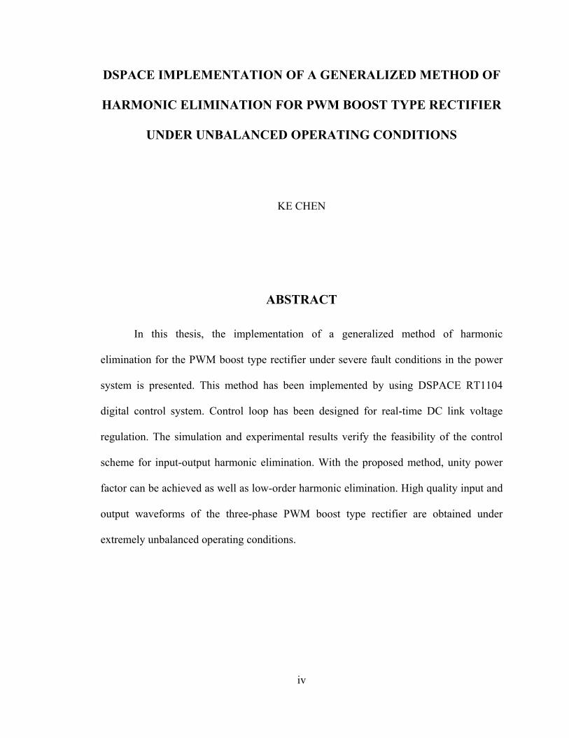


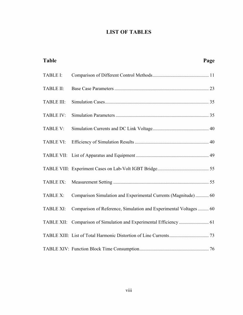


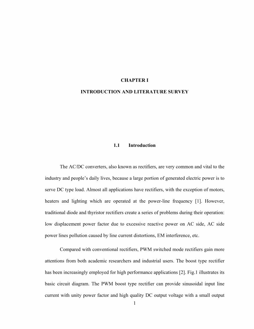


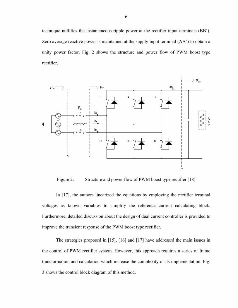

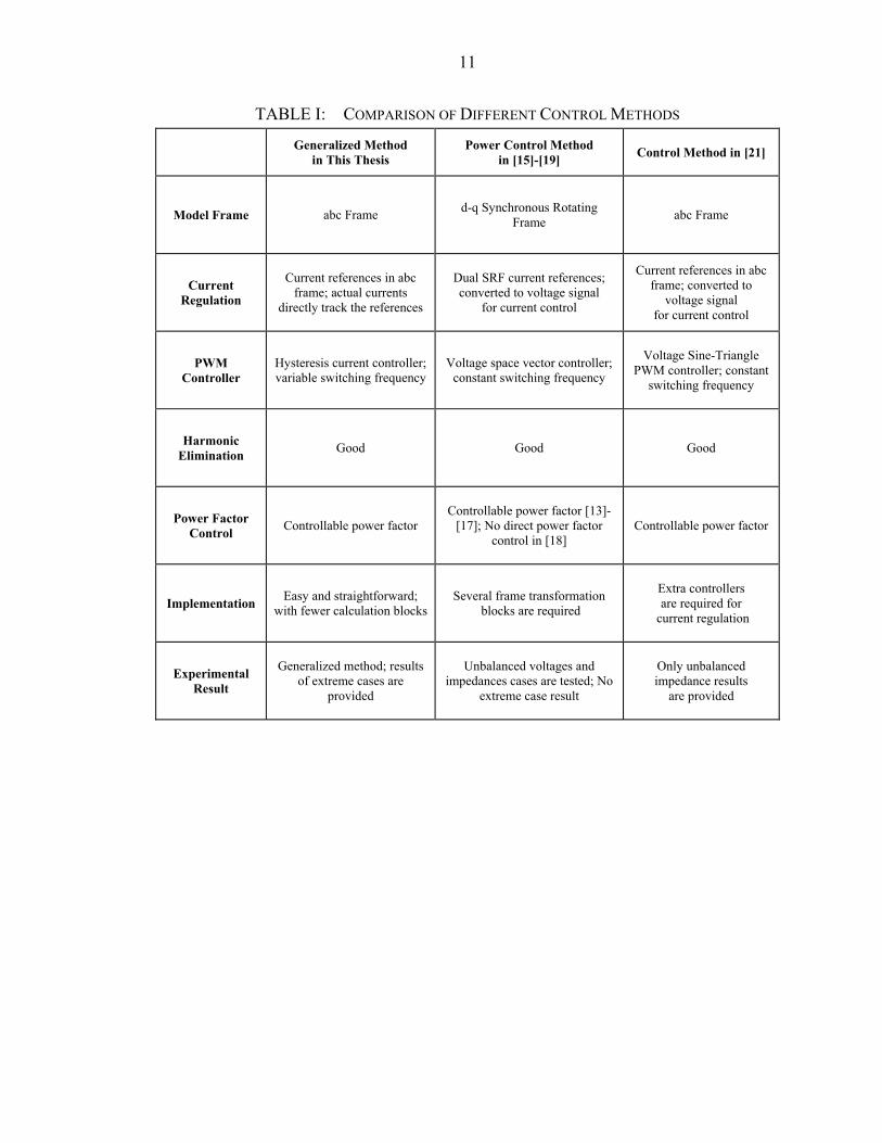
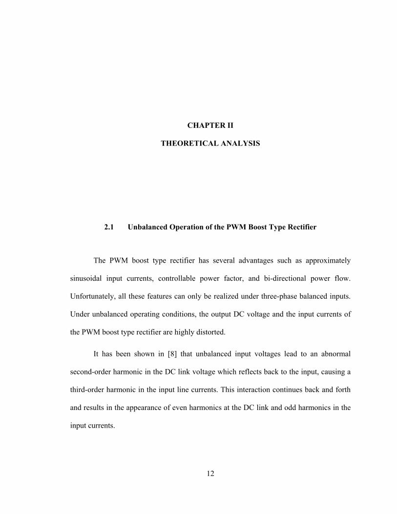
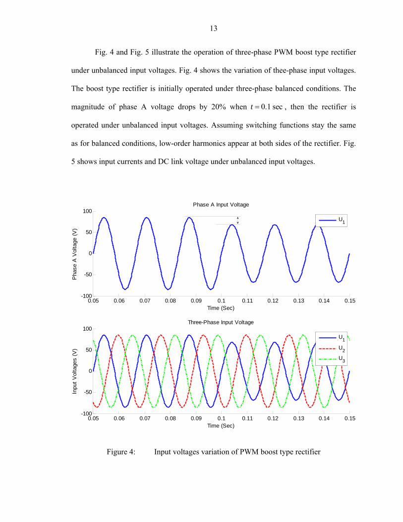
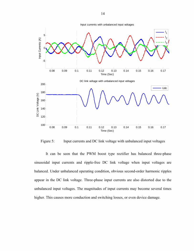
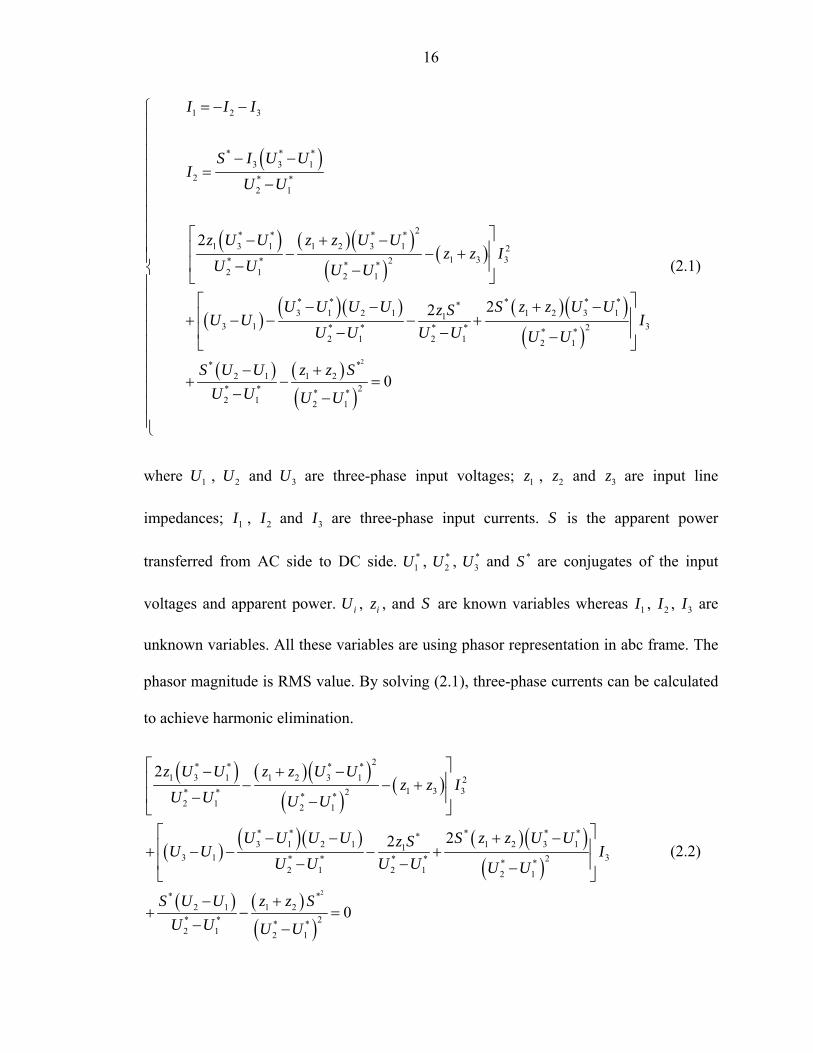


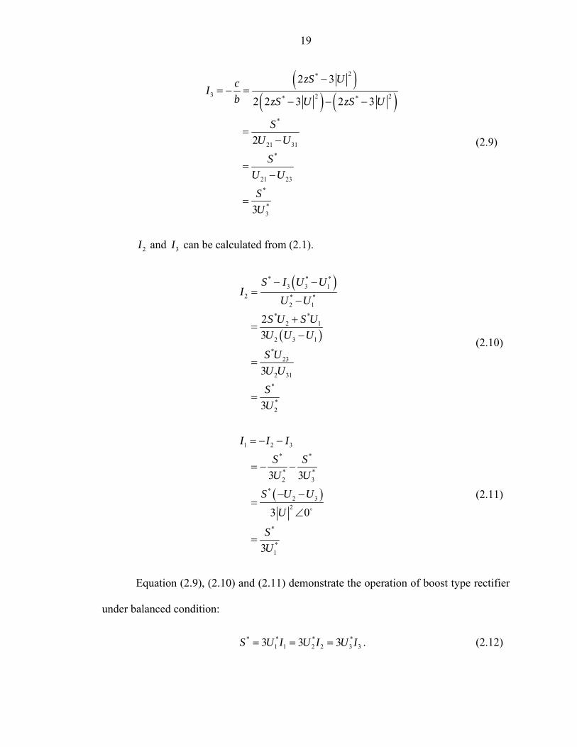

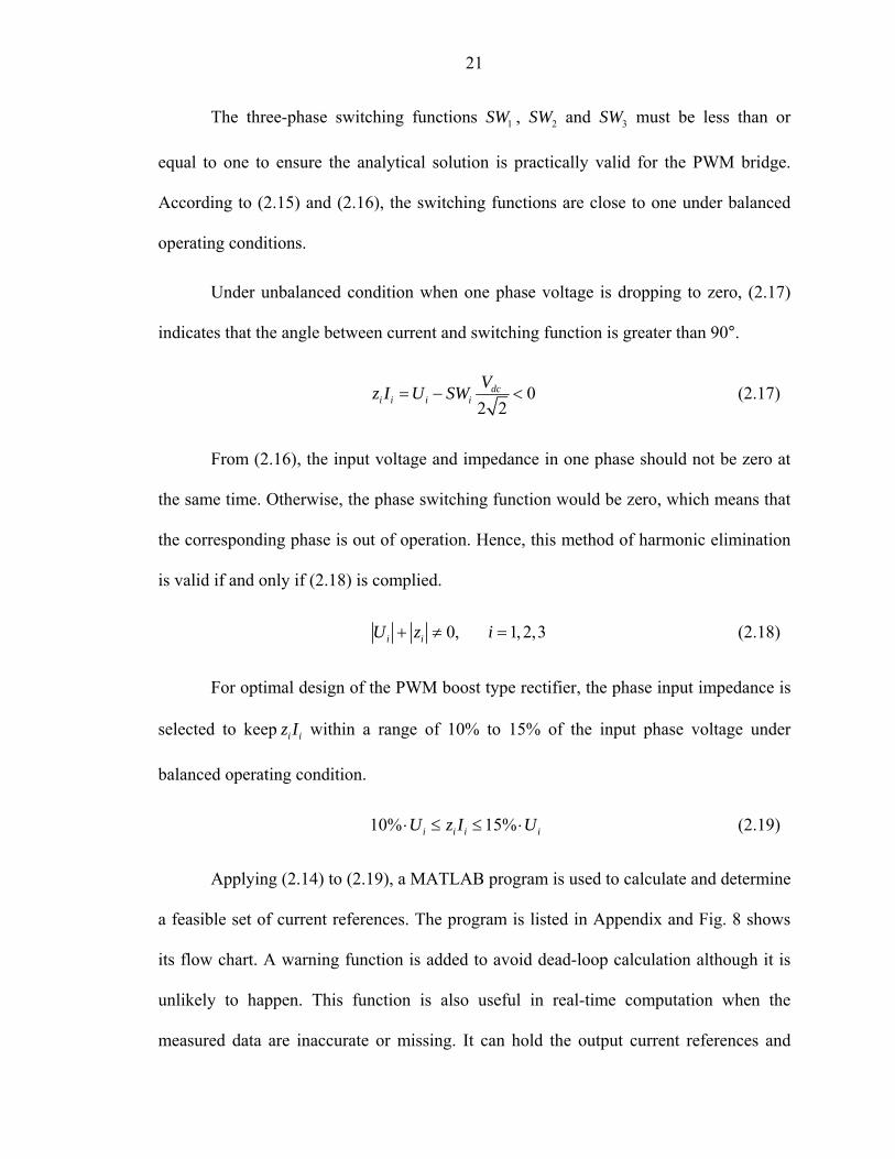
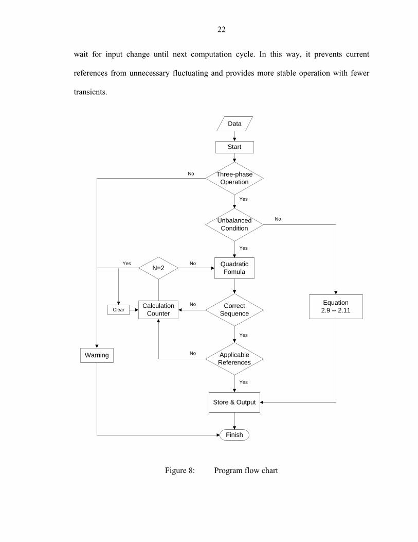
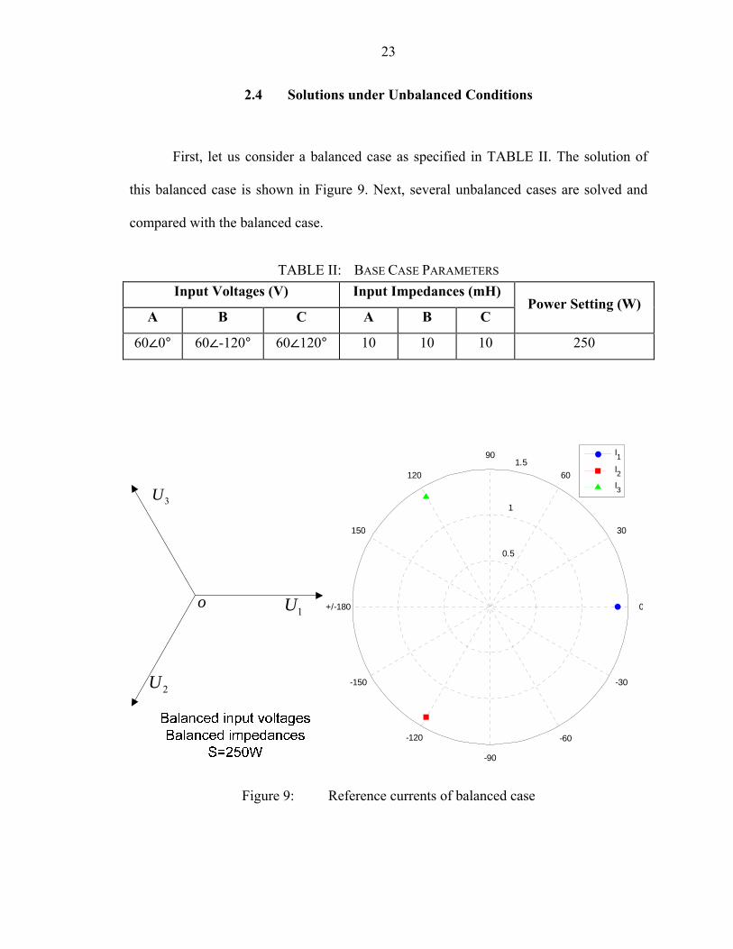

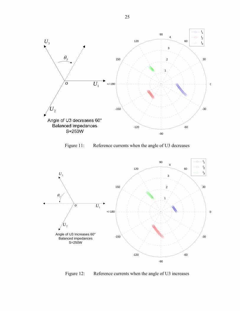
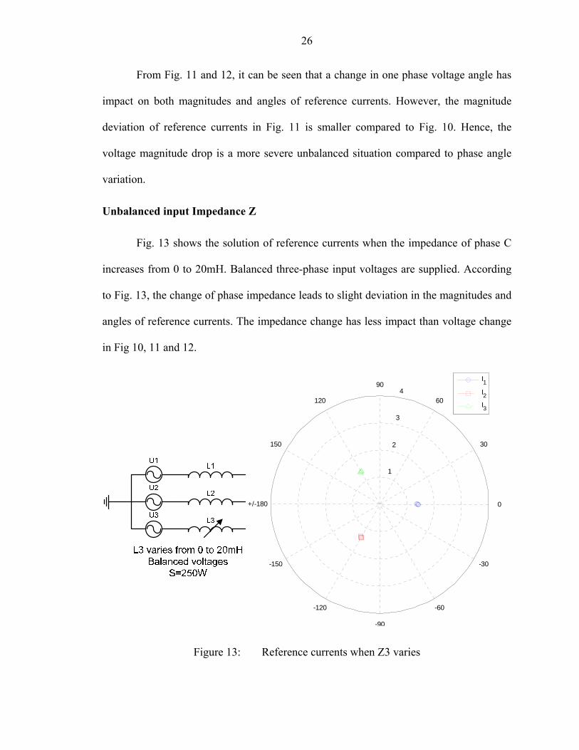


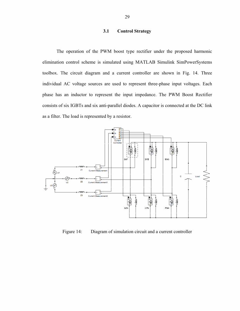
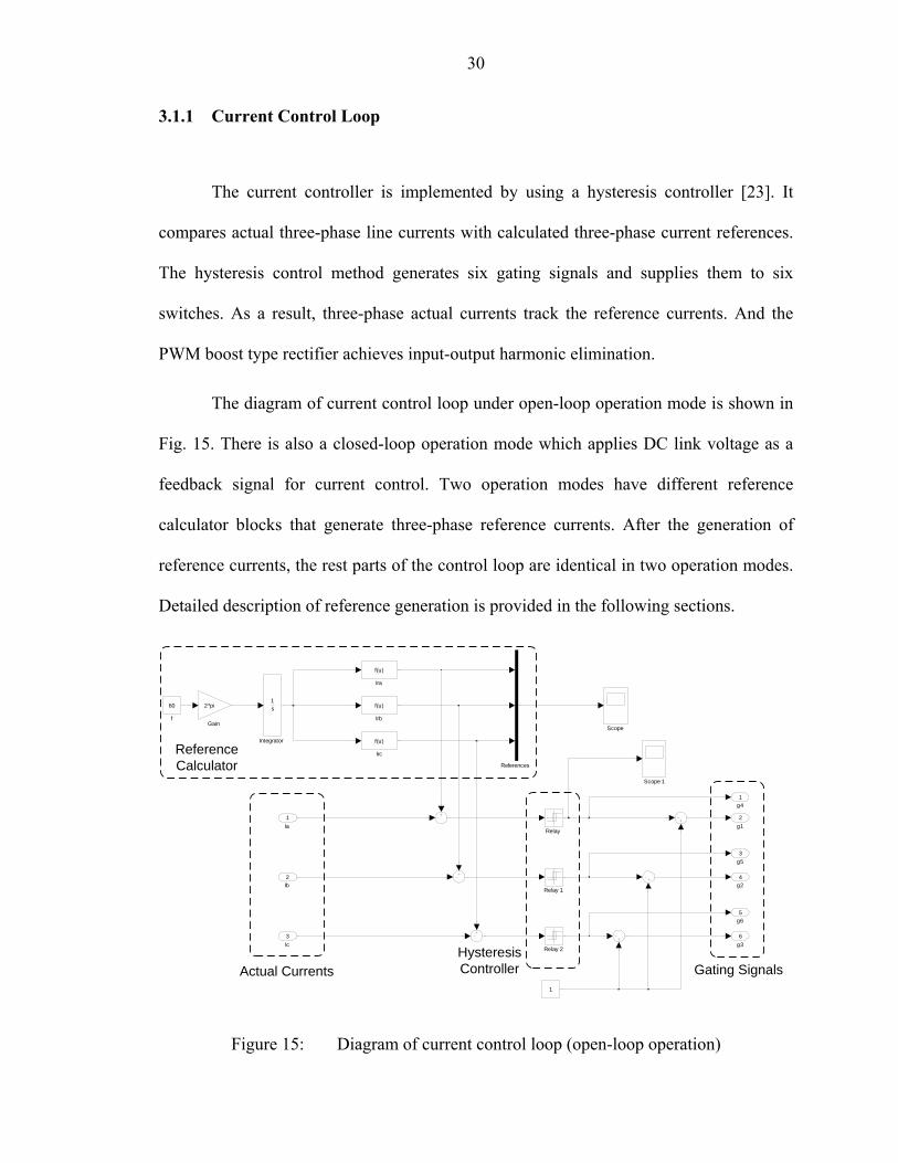
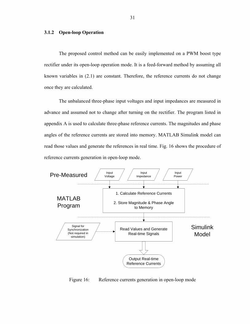
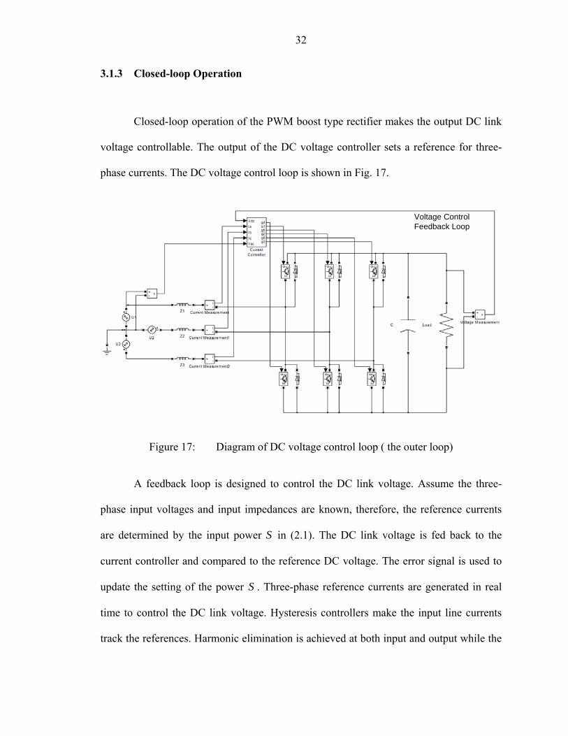
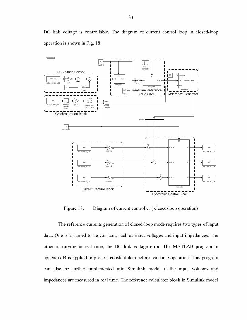

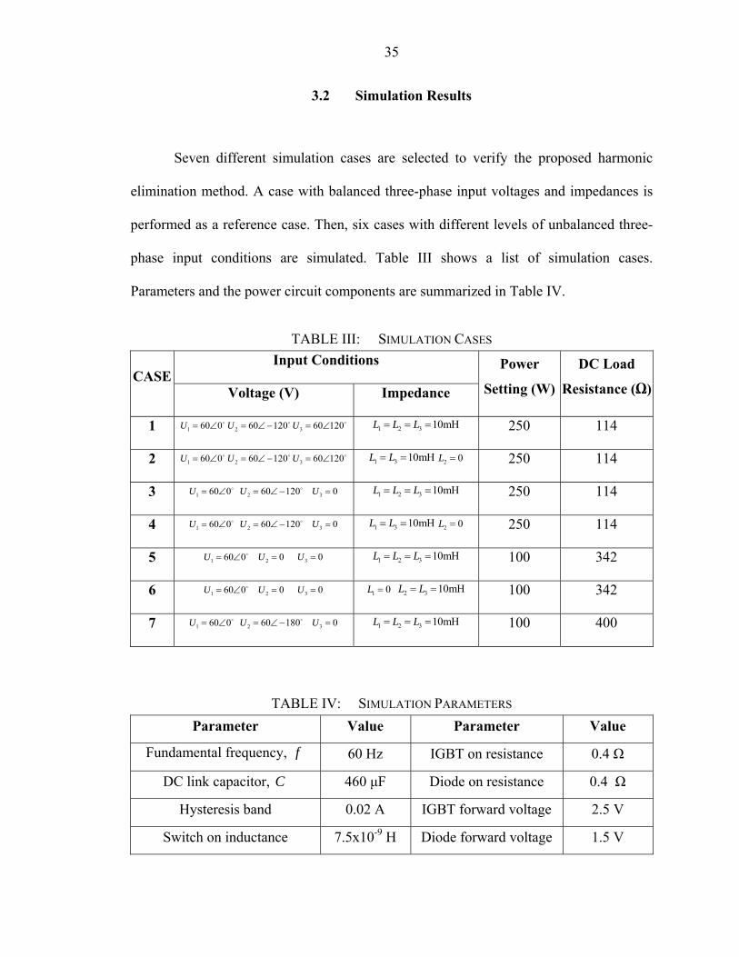
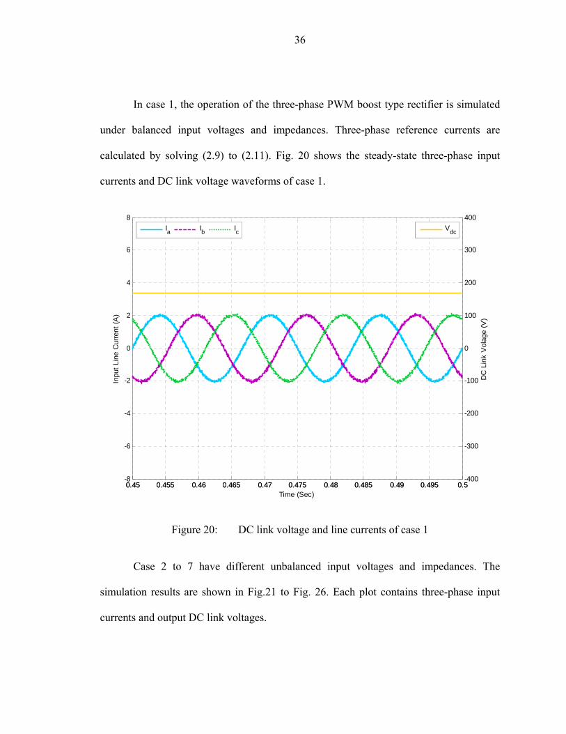
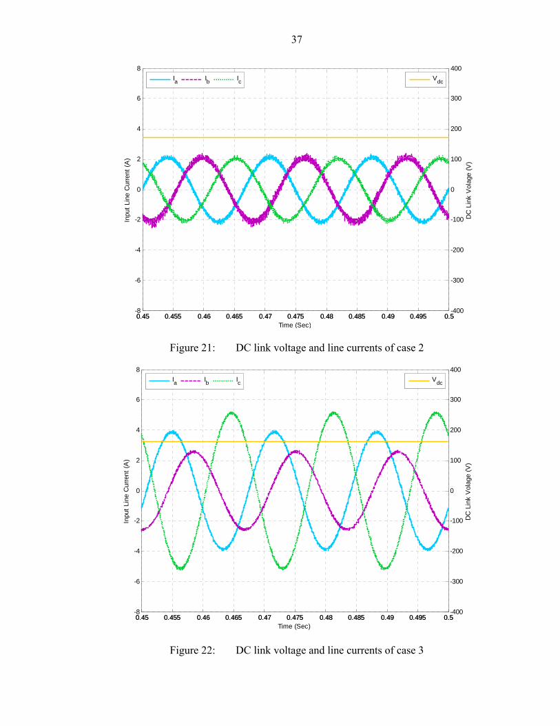
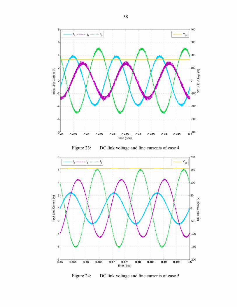

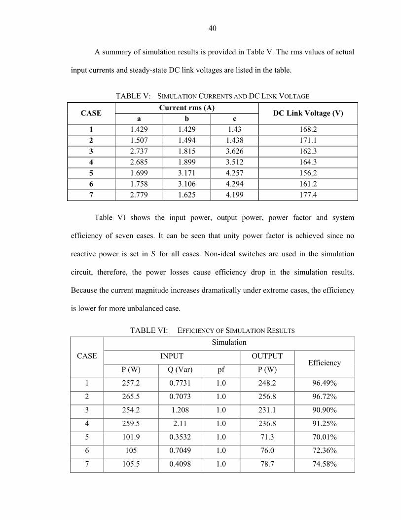


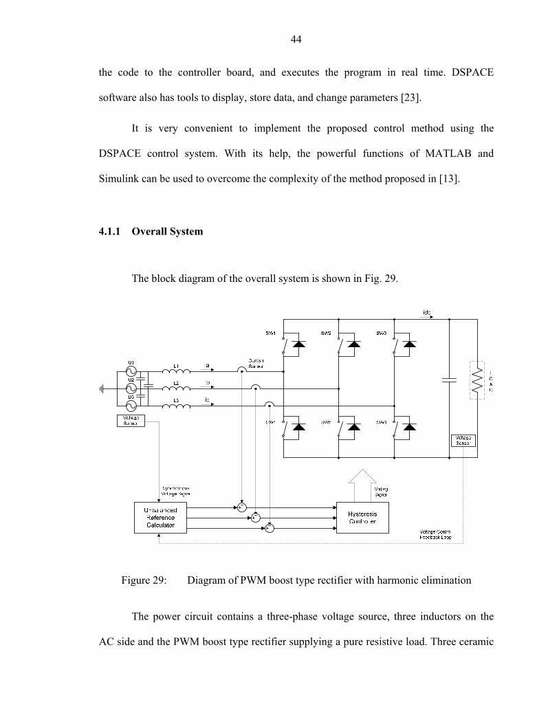

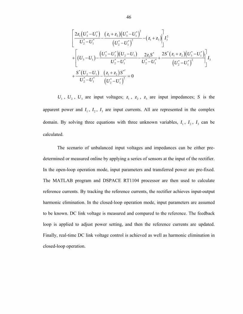
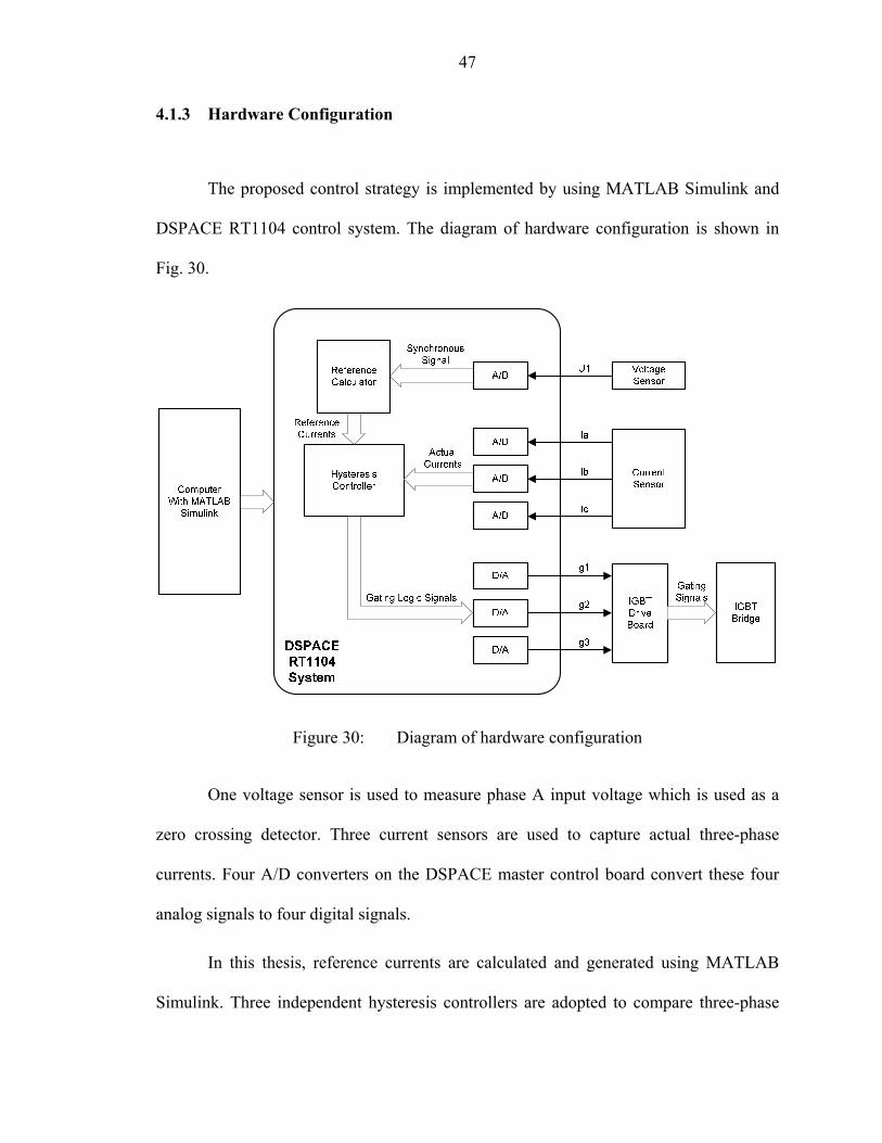
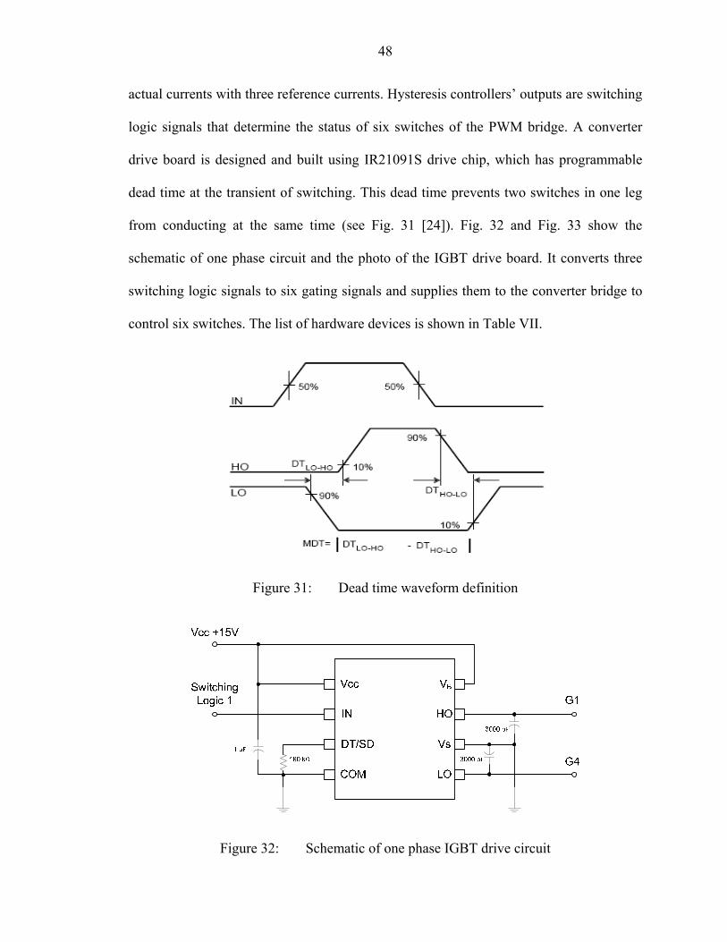
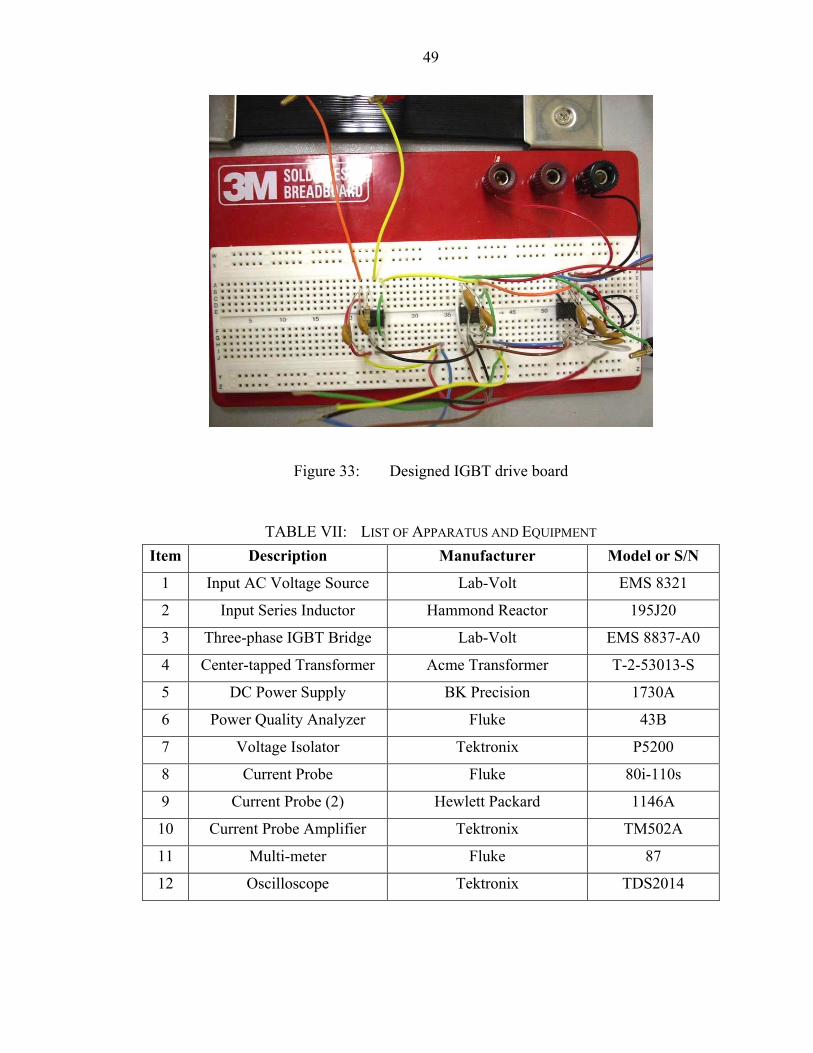
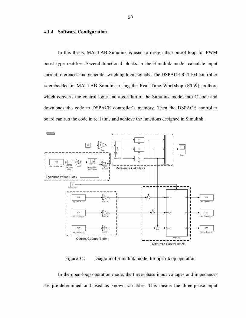


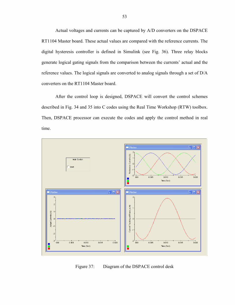

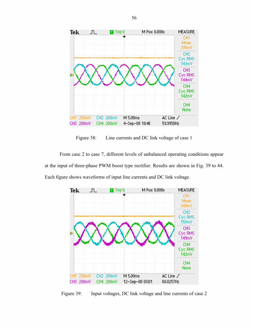
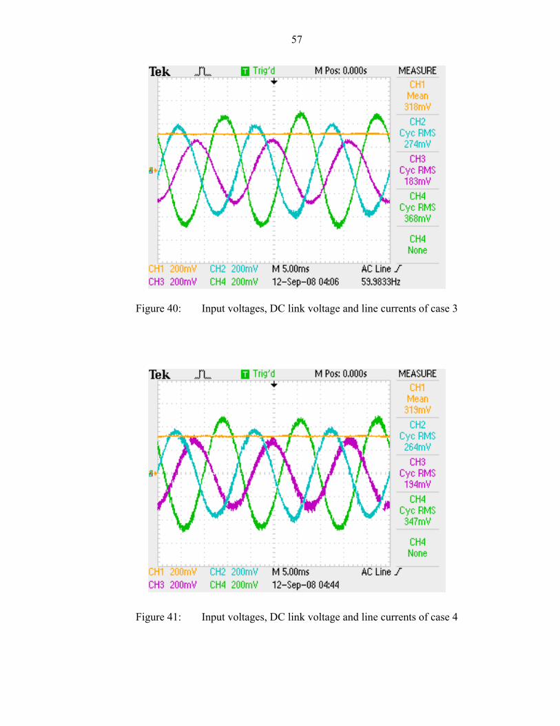
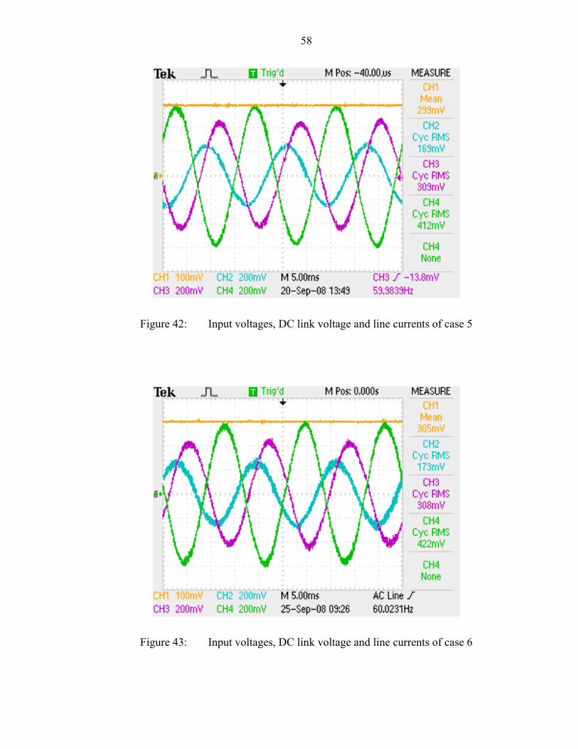

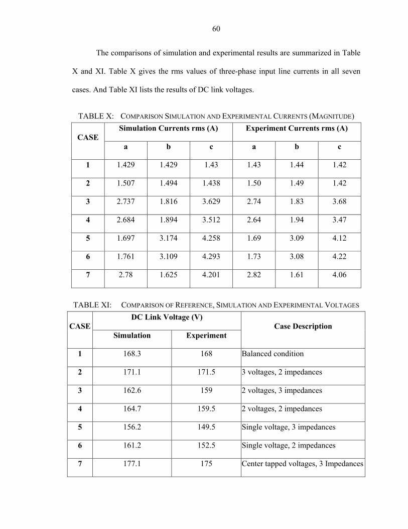
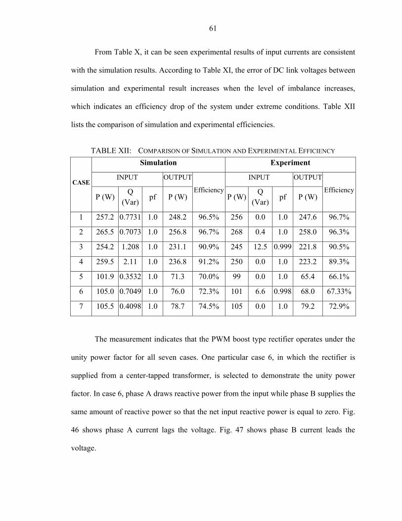

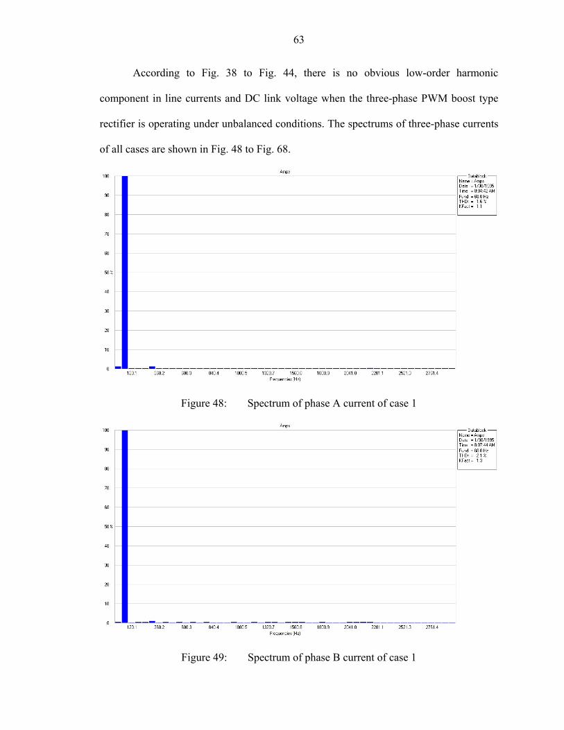
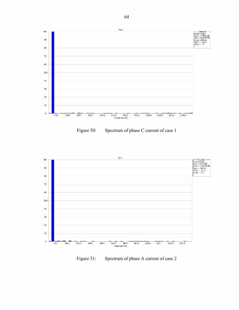

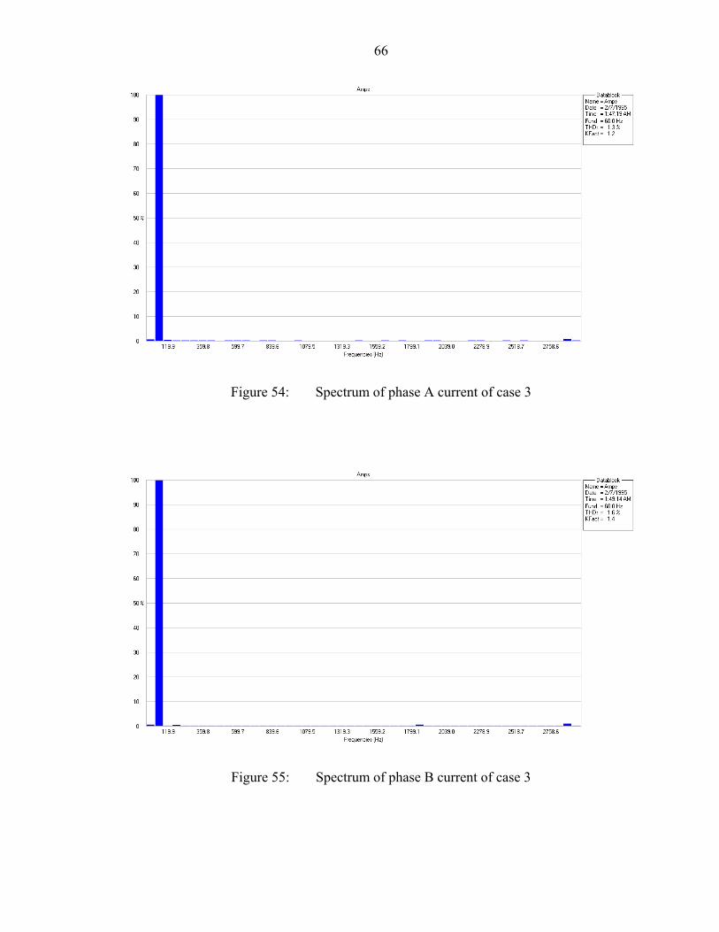

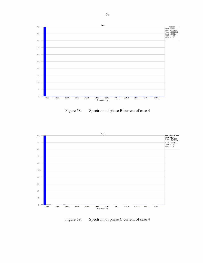


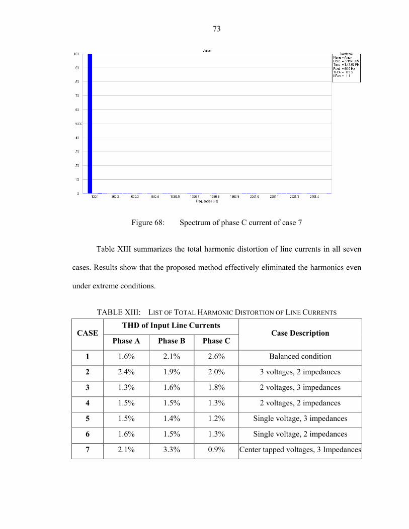
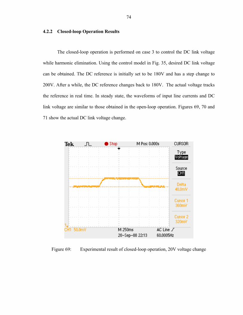


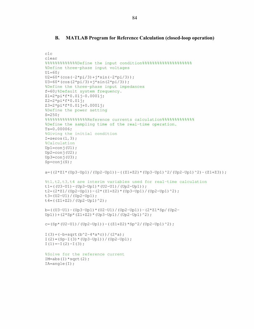
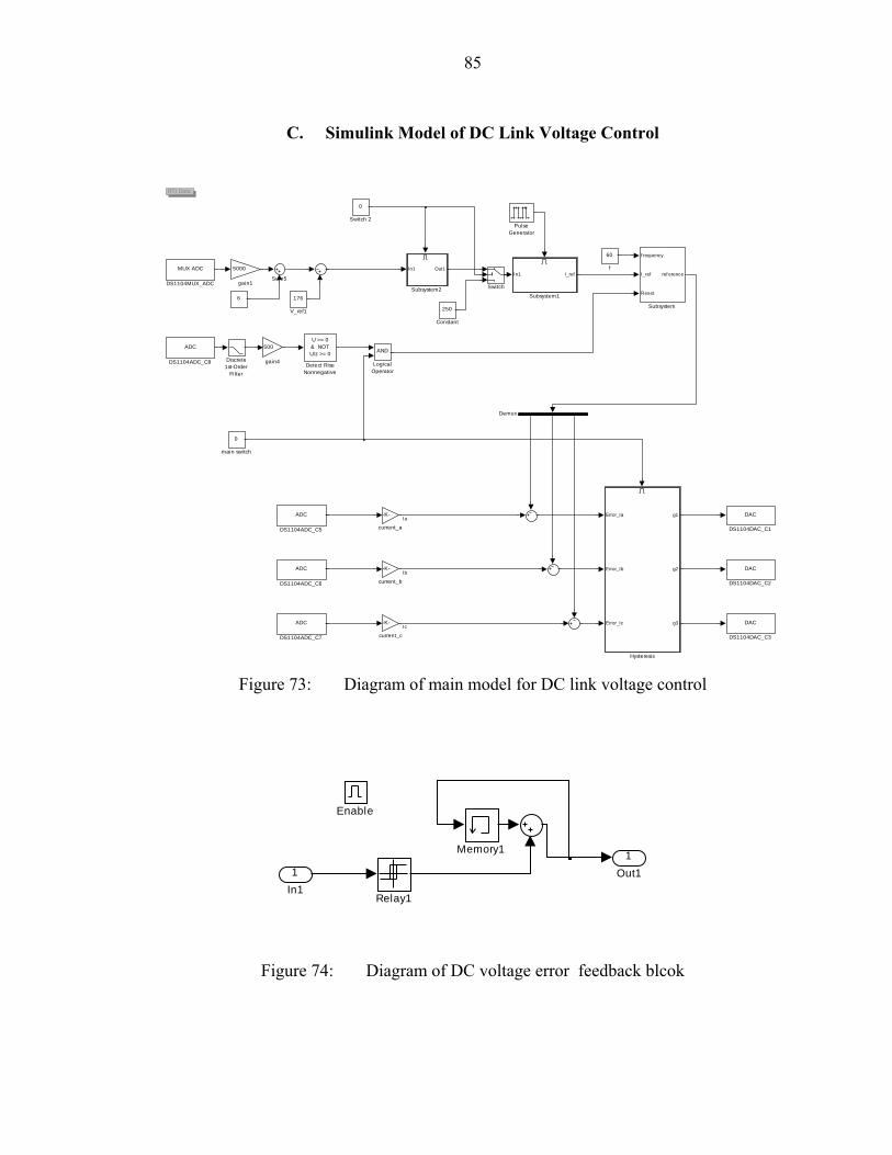
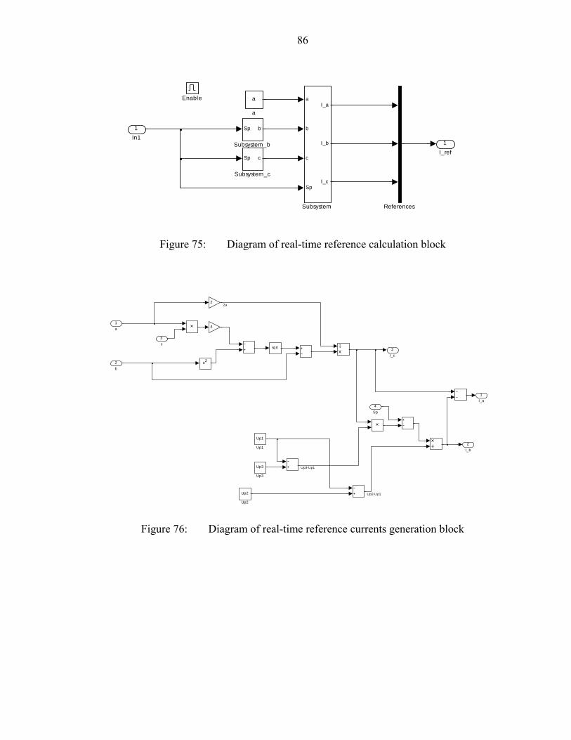


![Applied and Computational Harmonic Analysisbig · functions [13]. Note that Gelfand and Vilenkin only define non-periodic white noises, as generalized pro-cesses, i.e. random elements](https://static.documents.pub/doc/80x56/5f9ef93f1391b8740a4b989a/applied-and-computational-harmonic-functions-13-note-that-gelfand-and-vilenkin.jpg)

![Francisco Nettel · 2018-05-08 · arXiv:1502.01012v1 [math-ph] 3 Feb 2015 Topological quantization of gravitational fields as generalized harmonic maps Francisco Nettel∗ Dipartimento](https://static.documents.pub/doc/80x56/5c666a2209d3f252168c530b/francisco-nettel-2018-05-08-arxiv150201012v1-math-ph-3-feb-2015-topological.jpg)


