2016-2019 Microchip Technology Inc. DS70005280C-page 1 HIGHLIGHTS This section of the manual contains the following major topics: 1.0 Introduction ....................................................................................................................... 2 2.0 Module Description ........................................................................................................... 3 3.0 Control Registers .............................................................................................................. 4 4.0 Configuration and Operation ........................................................................................... 13 5.0 Application Information ................................................................................................... 20 6.0 Limitations ....................................................................................................................... 26 7.0 Related Application Notes............................................................................................... 27 8.0 Revision History .............................................................................................................. 28 High-Speed Analog Comparator with Slope Compensation DAC
Transcript
High-Speed Analog Comparator with Slope Compensation DAC
HIGHLIGHTS
This section of the manual contains the following major topics:
7.0 Related Application Notes............................................................................................... 27
8.0 Revision History .............................................................................................................. 28
2016-2019 Microchip Technology Inc. DS70005280C-page 1
dsPIC33/PIC24 Family Reference Manual
1.0 INTRODUCTION
The High-Speed Analog Comparator with Slope Compensation DAC module provides a way tomonitor voltage, current and other critical signals in a power conversion application that may betoo fast for the CPU and ADC to capture. Each High-Speed Analog Comparator module iscomprised of a high-speed comparator, Pulse Density Modulation (PDM) DAC and a slopecompensation unit.
The number of instances of the DAC/comparator modules is device-dependent. Refer to thedevice-specific data sheet for availability. The comparator module can be used to implementPeak Current mode control, Critical Conduction mode and hysteretic control-based powersupplies.
The High-Speed Analog Comparator with Slope Compensation DAC consists of the following keyfeatures:
• Rail-to-Rail Analog Comparator
• Up to Five Selectable Input Sources per Comparator:
- Up to four external inputs
- Up to two internal inputs from the PGA module
• Programmable Comparator Hysteresis
• Programmable Output Polarity
• Interrupt Generation Capability
• Dedicated Pulse Density Modulation (PDM) Digital-to-Analog Converter (DAC) for Each Analog Comparator:
- 12-bit resolution
• Multimode Multipole RC Output Filter:
- Transition mode: Provides the fastest response
- Fast mode: For tracking DAC slopes
- Steady-State mode: Provides 12-bit resolution
• Dedicated Support for the Following Modes:
- Slope Generation
- Hysteretic Control
- Triangle Wave
• Functional Support for the High-Speed PWM Module which Includes:
- PWM duty cycle control
- PWM period control
- PWM Fault detect
Note: This family reference manual section is meant to serve as a complement to devicedata sheets. Depending on the device, this manual section may not apply to alldsPIC33/PIC24 devices. Some dsPIC33/PIC24 devices are dual core and containboth a Master and Slave CPU core. For single core dsPIC33/PIC24 devices,disregard any Slave-specific references.
Please consult the note at the beginning of the “High-Speed Analog Comparatorwith Slope Compensation DAC” chapter in the current device data sheet to checkwhether this document supports the device you are using.
Device data sheets and family reference manual sections are available fordownload from the Microchip Worldwide Website at: http://www.microchip.com.
DS70005280C-page 2 2016-2019 Microchip Technology Inc.
High-Speed Analog Comparator with Slope Compensation DAC
2.0 MODULE DESCRIPTION
The High-Speed Analog Comparator with Slope Compensation DAC module is comprised of ahigh-speed comparator, Pulse Density Modulation (PDM) DAC and a slope compensation unit.Devices typically have multiple instances of the module. Refer to the specific device data sheetfor the number of available modules.
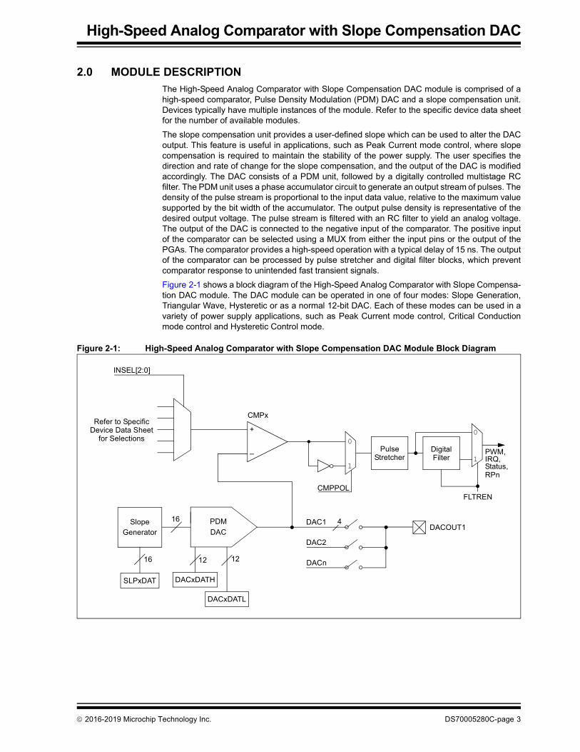
The slope compensation unit provides a user-defined slope which can be used to alter the DACoutput. This feature is useful in applications, such as Peak Current mode control, where slopecompensation is required to maintain the stability of the power supply. The user specifies thedirection and rate of change for the slope compensation, and the output of the DAC is modifiedaccordingly. The DAC consists of a PDM unit, followed by a digitally controlled multistage RCfilter. The PDM unit uses a phase accumulator circuit to generate an output stream of pulses. Thedensity of the pulse stream is proportional to the input data value, relative to the maximum valuesupported by the bit width of the accumulator. The output pulse density is representative of thedesired output voltage. The pulse stream is filtered with an RC filter to yield an analog voltage.The output of the DAC is connected to the negative input of the comparator. The positive inputof the comparator can be selected using a MUX from either the input pins or the output of thePGAs. The comparator provides a high-speed operation with a typical delay of 15 ns. The outputof the comparator can be processed by pulse stretcher and digital filter blocks, which preventcomparator response to unintended fast transient signals.
Figure 2-1 shows a block diagram of the High-Speed Analog Comparator with Slope Compensa-tion DAC module. The DAC module can be operated in one of four modes: Slope Generation,Triangular Wave, Hysteretic or as a normal 12-bit DAC. Each of these modes can be used in avariety of power supply applications, such as Peak Current mode control, Critical Conductionmode control and Hysteretic Control mode.
Figure 2-1: High-Speed Analog Comparator with Slope Compensation DAC Module Block Diagram
INSEL[2:0]
+
–
SlopeGenerator
CMPx
0
1
CMPPOL
PWM,
SLPxDAT DACxDATH
DAC1
DAC2
DACn
DACOUT1
DACxDATL
DigitalFilter
0
1 IRQ,Status,
FLTREN
16 12 12
16
PulseStretcher
PDM
DAC
RPn
Refer to SpecificDevice Data Sheet
for Selections
4
2016-2019 Microchip Technology Inc. DS70005280C-page 3
dsP
IC3
3/PIC
24 F
amily
Re
feren
ce M
an
ual
DS
70
00
52
80
C-p
ag
e 4
2
01
6-2
01
9 M
icroch
ip T
ech
no
log
y Inc.
ACCTRL1 and DACCTRL2, specify commonnstance ‘x’. Devices that support both Master
ed in Table 3-1.
Bit 4 Bit 3 Bit 2 Bit 1 Bit 0
1:0] — FCLKDIV[2:0]
]
:0]
SEL[2:0] HYSPOL HYSSEL[1:0]
— — — — —
SLPSTRT[3:0]
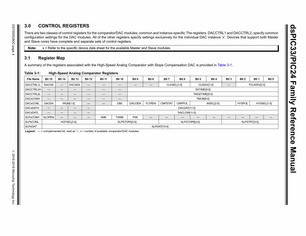
3.0 CONTROL REGISTERS
There are two classes of control registers for the comparator/DAC modules: common and instance-specific.The registers, Dconfiguration settings for the DAC modules. All of the other registers specify settings exclusively for the individual DAC iand Slave cores have complete and separate sets of control registers.
3.1 Register Map
A summary of the registers associated with the High-Speed Analog Comparator with Slope Compensation DAC is provid
Note: x = Refer to the specific device data sheet for the available Master and Slave modules.
Table 3-1: High-Speed Analog Comparator Registers
File Name Bit 15 Bit 14 Bit 13 Bit 12 Bit 11 Bit 10 Bit 9 Bit 8 Bit 7 Bit 6 Bit 5
Legend: — = unimplemented bit, read as ‘0’; x = number of available comparator/DAC modules.
High-Speed Analog Comparator with Slope Compensation DAC
Register 3-1: DACCTRL1L: DAC Control 1 Low Register
R/W-0 U-0 R/W-0 U-0 U-0 U-0 U-0 U-0
DACON — DACSIDL — — — — —
bit 15 bit 8
R/W-0 R/W-0 R/W-0 R/W-0 U-0 R/W-0 R/W-0 R/W-0
CLKSEL[1:0](1) CLKDIV[1:0](1) — FCLKDIV[2:0](2)
bit 7 bit 0
Legend:
R = Readable bit W = Writable bit U = Unimplemented bit, read as ‘0’
-n = Value at POR ‘1’ = Bit is set ‘0’ = Bit is cleared
bit 15 DACON: Common DAC Module Enable bit
1 = Enables DAC modules0 = Disables DAC modules
bit 14 Unimplemented: Read as ‘0’
bit 13 DACSIDL: DAC Stop in Idle mode bit
1 = Discontinues module operation when device enters Idle mode0 = Continues module operation in Idle mode
bit 12-8 Unimplemented: Read as ‘0’
bit 7-6 CLKSEL[1:0]: DAC Clock Source Select bits(1)
Refer to device-specific data sheet for selections.
bit 5-4 CLKDIV[1:0]: Clock Divider bits(1)
11 = Divide by 410 = Divide by 3 (non-uniform duty cycle)01 = Divide by 200 = 1x
bit 3 Unimplemented: Read as ‘0’
bit 2-0 FCLKDIV[2:0]: Comparator Filter Clock Divider bits(2)
111 = Divide by 8110 = Divide by 7101 = Divide by 6100 = Divide by 5011 = Divide by 4010 = Divide by 3001 = Divide by 2000 = 1x
Note 1: These bits should only be changed when DACON = 0 to avoid unpredictable behavior.
2: The input clock to this divider is the selected clock input, CLKSEL[1:0], and then divided by two.
2016-2019 Microchip Technology Inc. DS70005280C-page 5
dsPIC33/PIC24 Family Reference Manual
Register 3-2: DACCTRL2H: DAC Control 2 High Register
U-0 U-0 U-0 U-0 U-0 U-0 R/W-0 R/W-0
— — — — — — SSTIME[9:8](1,2)
bit 15 bit 8
R/W-1 R/W-0 R/W-0 R/W-0 R/W-1 R/W-0 R/W-1 R/W-0
SSTIME[7:0](1,2)
bit 7 bit 0
Legend:
R = Readable bit W = Writable bit U = Unimplemented bit, read as ‘0’
-n = Value at POR ‘1’ = Bit is set ‘0’ = Bit is cleared
bit 15-10 Unimplemented: Read as ‘0’
bit 9-0 SSTIME[9:0]: Transition Start Mode until Steady-State Filter is Enabled bits(1,2)
Note 1: The value for SSTIME[9:0] should be greater than the TMODTIME[9:0] bits.
2: Default value for SSTIME[9:0] = 0x8A.
Register 3-3: DACCTRL2L: DAC Control 2 Low Register
U-0 U-0 U-0 U-0 U-0 U-0 R/W-0 R/W-0
— — — — — — TMODTIME[9:8](1,2)
bit 15 bit 8
R/W-0 R/W-1 R/W-0 R/W-1 R/W-0 R/W-1 R/W-0 R/W-1
TMODTIME[7:0](1,2)
bit 7 bit 0
Legend:
R = Readable bit W = Writable bit U = Unimplemented bit, read as ‘0’
-n = Value at POR ‘1’ = Bit is set ‘0’ = Bit is cleared
bit 15-10 Unimplemented: Read as ‘0’
bit 9-0 TMODTIME[9:0]: Duration of Transition Mode bits(1,2)
Note 1: The value for TMODTIME[9:0] should be less than the SSTIME[9:0] bits.
2: Default value for TMODTIME[9:0] = 0x55.
DS70005280C-page 6 2016-2019 Microchip Technology Inc.
High-Speed Analog Comparator with Slope Compensation DAC
Register 3-4: DACxCONH: DACx Control High Register
U-0 U-0 U-0 U-0 U-0 U-0 R/W-0 R/W-0
— — — — — — TMCB[9:8]
bit 15 bit 8
R/W-0 R/W-0 R/W-0 R/W-0 R/W-0 R/W-0 R/W-0 R/W-0
TMCB[7:0]
bit 7 bit 0
Legend:
R = Readable bit W = Writable bit U = Unimplemented bit, read as ‘0’
-n = Value at POR ‘1’ = Bit is set ‘0’ = Bit is cleared
bit 15-10 Unimplemented: Read as ‘0’
bit 9-0 TMCB[9:0]: DACx Leading-Edge Blanking bits
This register specifies the blanking period in counts of 2/FDAC for the comparator following changes to the DACx output during Change-of-State (COS) for the input signal selected by the HCFSEL[3:0] bits in Register 3-9.
Register 3-5: DACxCONL: DACx Control Low Register
R/W-0 R/W-0 R/W-0 U-0 U-0 R/W-0 R/W-0 R/W-0
DACEN IRQM[1:0](1,2) — — CBE DACOEN FLTREN
bit 15 bit 8
R-0 R/W-0 R/W-0 R/W-0 R/W-0 R/W-0 R/W-0 R/W-0
CMPSTAT CMPPOL INSEL[2:0] HYSPOL HYSSEL[1:0]
bit 7 bit 0
Legend:
R = Readable bit W = Writable bit U = Unimplemented bit, read as ‘0’
-n = Value at POR ‘1’ = Bit is set ‘0’ = Bit is cleared
bit 15 DACEN: Individual DACx Module Enable bit
1 = Enables DACx module0 = Disables DACx module and disables FSCM clock to reduce power consumption; any pending Slope
mode and/or underflow conditions are cleared
bit 14-13 IRQM[1:0]: Interrupt Mode Select bits(1,2)
11 = Generates an interrupt on either a rising or falling edge detect10 = Generates an interrupt on a falling edge detect01 = Generates an interrupt on a rising edge detect00 = Interrupts are disabled
bit 12-11 Unimplemented: Read as ‘0’
Note 1: Changing these bits during operation may generate a spurious interrupt.2: The edge selection is a post-polarity selection via the CMPPOL bit.
2016-2019 Microchip Technology Inc. DS70005280C-page 7
dsPIC33/PIC24 Family Reference Manual
bit 10 CBE: Comparator Blank Enable bit
1 = Enables the analog comparator output to be blanked (gated off) during the recovery transitionfollowing the completion of a slope operation
0 = Disables the blanking signal to the analog comparator; therefore, the analog comparator output isalways active
bit 9 DACOEN: DACx Output Buffer Enable bit
1 = DACx analog voltage is connected to the DACOUT1 pin0 = DACx analog voltage is not connected to the DACOUT1 pin
bit 8 FLTREN: Comparator Digital Filter Enable bit
1 = Digital filter is enabled0 = Digital filter is disabled
bit 7 CMPSTAT: Comparator Status bit
Current state of the comparator output including the CMPPOL selection.
bit 6 CMPPOL: Comparator Output Polarity Control bit
1 = Output is inverted0 = Output is noninverted
bit 5-3 INSEL[2:0]: Comparator Input Source Select bits
See device-specific data sheet for selections.
bit 2 HYSPOL: Comparator Hysteresis Polarity Select bit
1 = Hysteresis is applied to the falling edge of the comparator output0 = Hysteresis is applied to the rising edge of the comparator output
bit 1-0 HYSSEL[1:0]: Comparator Hysteresis Select bits
11 = 45 mV hysteresis10 = 30 mV hysteresis01 = 15 mV hysteresis00 = No hysteresis is selected
Register 3-5: DACxCONL: DACx Control Low Register (Continued)
Note 1: Changing these bits during operation may generate a spurious interrupt.2: The edge selection is a post-polarity selection via the CMPPOL bit.
DS70005280C-page 8 2016-2019 Microchip Technology Inc.
High-Speed Analog Comparator with Slope Compensation DAC
Register 3-6: DACxDATH: DACx Data High Register
U-0 U-0 U-0 U-0 R/W-0 R/W-0 R/W-0 R/W-0
— — — — DACDAT[11:8](1)
bit 15 bit 8
R/W-0 R/W-0 R/W-0 R/W-0 R/W-0 R/W-0 R/W-0 R/W-0
DACDAT[7:0](1)
bit 7 bit 0
Legend:
R = Readable bit W = Writable bit U = Unimplemented bit, read as ‘0’
-n = Value at POR ‘1’ = Bit is set ‘0’ = Bit is cleared
bit 15-12 Unimplemented: Read as ‘0’
bit 11-0 DACDAT[11:0]: DACx Data bits(1)
This register specifies the high DACx data value, VDAC = DACDAT * (AVDD)/4095. Valid values are from 205 (0x0CD) to 3890 (0xF32).111100110011 to 111111111111 = Reserved111100110010 = 0.95 * AVDD
••11001101 = 0.05 * AVDD
000000000000 to 11001100 = Reserved
Note 1: When operating in Slope mode or Triangle Wave mode, the DACDATx value must be greater or equal to (5 x SLPDATx) + DACLOWx.
2016-2019 Microchip Technology Inc. DS70005280C-page 9
dsPIC33/PIC24 Family Reference Manual
Register 3-7: DACxDATL: DACx Data Low Register
U-0 U-0 U-0 U-0 R/W-0 R/W-0 R/W-0 R/W-0
— — — — DACLOW[11:8](1)
bit 15 bit 8
R/W-0 R/W-0 R/W-0 R/W-0 R/W-0 R/W-0 R/W-0 R/W-0
DACLOW[7:0](1)
bit 7 bit 0
Legend:
R = Readable bit W = Writable bit U = Unimplemented bit, read as ‘0’
-n = Value at POR ‘1’ = Bit is set ‘0’ = Bit is cleared
bit 15-12 Unimplemented: Read as ‘0’
bit 11-0 DACLOW[11:0]: DACx Low Data bits(1)
In Hysteretic mode, Slope Generator mode and Triangle mode, this register specifies the low data value and/or limit for the DACx module. VOUT = DACDATx * (AVDD)/4095. Valid values are from 205 (0x0CD) to 3890 (0xF32).
111100110011 to 111111111111 = Reserved111100110010 = 0.95 * AVDD
••11001101 = 0.05 * AVDD
000000000000 to 11001100 = Reserved
Note 1: When operating in Slope mode or Triangle Wave mode, the DACLOWx value must be less than or equal to DACDATx – (5 x SLPDATx).
DS70005280C-page 10 2016-2019 Microchip Technology Inc.
High-Speed Analog Comparator with Slope Compensation DAC
Register 3-8: SLPxCONH: DACx Slope Control High Register
R/W-0 U-0 U-0 U-0 R/W-0 R/W-0 R/W-0 U-0
SLOPEN — — — HME(1) TWME(2) PSE —
bit 15 bit 8
U-0 U-0 U-0 U-0 U-0 U-0 U-0 U-0
— — — — — — — —
bit 7 bit 0
Legend:
R = Readable bit W = Writable bit U = Unimplemented bit, read as ‘0’
-n = Value at POR ‘1’ = Bit is set ‘0’ = Bit is cleared
bit 15 SLOPEN: Slope Function Enable/On bit
1 = Enables slope function0 = Disables slope function; slope accumulator is disabled to reduce power consumption
bit 14-12 Unimplemented: Read as ‘0’
bit 11 HME: Hysteretic Mode Enable bit(1)
1 = Enables Hysteretic mode for DACx0 = Disables Hysteretic mode for DACx
bit 10 TWME: Triangle Wave Mode Enable bit(2)
1 = Enables Triangle Wave mode for DACx0 = Disables Triangle Wave mode for DACx
bit 9 PSE: Positive Slope Mode Enable bit
1 = Slope mode is positive (increasing)0 = Slope mode is negative (decreasing)
bit 8-0 Unimplemented: Read as ‘0’
Note 1: HME mode requires the user to disable the slope function (SLOPEN = 0).2: TWME mode requires the user to enable the slope function (SLOPEN = 1).
2016-2019 Microchip Technology Inc. DS70005280C-page 11
dsPIC33/PIC24 Family Reference Manual
Register 3-9: SLPxCONL: DACx Slope Control Low Register
R/W-0 R/W-0 R/W-0 R/W-0 R/W-0 R/W-0 R/W-0 R/W-0
HCFSEL[3:0] SLPSTOPA[3:0]
bit 15 bit 8
R/W-0 R/W-0 R/W-0 R/W-0 R/W-0 R/W-0 R/W-0 R/W-0
SLPSTOPB[3:0] SLPSTRT[3:0]
bit 7 bit 0
Legend:
R = Readable bit W = Writable bit U = Unimplemented bit, read as ‘0’
-n = Value at POR ‘1’ = Bit is set0 ‘0’ = Bit is cleared
bit 15-12 HCFSEL[3:0]: Hysteretic Comparator Function Input Select bits
The selected input signal controls the switching between the DACx high limit (DACxDATH) and the DACxlow limit (DACxDATL) as the data source for the PDM DAC; it modifies the polarity of the comparator, andthe rising and falling edges initiate the start of the LEB counter (TMCB[9:0] bits in Register 3-4). See thedevice-specific data sheet for assignments.
bit 11-8 SLPSTOPA[3:0]: Slope Stop A Signal Select bits
The selected Slope Stop A signal is logically ORed with the selected Slope Stop B signal to terminatethe slope function. See the device-specific data sheet for assignments.
bit 7-4 SLPSTOPB[3:0]: Slope Stop B Signal Select bits
The selected Slope Stop B signal is logically ORed with the selected Slope Stop A signal to terminatethe slope function. See the device-specific data sheet for assignments.
bit 3-0 SLPSTRT[3:0]: Slope Start Signal Select bits
Register 3-10: SLPxDAT: DACx Slope Data Register(1)
R/W-0 R/W-0 R/W-0 R/W-0 R/W-0 R/W-0 R/W-0 R/W-0
SLPDAT[15:8]
bit 15 bit 8
R/W-0 R/W-0 R/W-0 R/W-0 R/W-0 R/W-0 R/W-0 R/W-0
SLPDAT[7:0]
bit 7 bit 0
Legend:
R = Readable bit W = Writable bit U = Unimplemented bit, read as ‘0’
-n = Value at POR ‘1’ = Bit is set ‘0’ = Bit is cleared
bit 15-0 SLPDAT[15:0]: Slope Ramp Rate Value in 12.4 Format bits
This value represents the number of counts the DAC changes in a 2/FDAC step.
Note 1: Register data are left justified.
DS70005280C-page 12 2016-2019 Microchip Technology Inc.
High-Speed Analog Comparator with Slope Compensation DAC
4.0 CONFIGURATION AND OPERATION
The High-Speed Analog Comparator with Slope Compensation DAC module is comprised ofvarious blocks, such as a comparator, DAC, etc. The functionality and configuration of differentblocks are discussed in this section.
4.1 Comparator Stage
4.1.1 COMPARATOR INPUTS
The inputs to the comparator module are configured using the DACxCONL register. Eachcomparator has up to five device-specific inputs, as shown in Figure 2-1. Refer to the device-specific data sheet for selections. The INSEL[2:0] bits (DACxCONL[5:3]) are used to select thecomparator input source. The positive input of the comparator is connected to one of the selectedinput sources, while the negative input is always internally connected to the DAC output.
4.1.2 COMPARATOR OUTPUTS
The comparator output can be used to trigger PWM modules or interrupts for action based on thecomparator event. When the digital filter is disabled, the comparator signal is made directly avail-able to the PWM module as a current limit and/or Fault signal. This ensures minimal latency forCurrent mode applications and for time-critical (safety) applications. The status signal and theinterrupt request signal will be processed by the pulse stretcher circuit. When the digital filter isenabled, the PWM trigger signal, status signal and interrupt request signal are all processed bythe pulse stretcher and the digital filter logic. This will cause a delay in the current limit/Fault limitevent. The polarity of the comparator output is selected by configuring the CMPPOL bit(DACxCONL[6]). The comparator output can be monitored on the I/O pin by configuring thePeripheral Pin Select (PPS) register.
4.1.3 COMPARATOR INTERRUPT
The analog comparator interrupt can be used to service the comparator switching event and canbe enabled or disabled from the interrupt controller. The analog comparator interrupt can be con-figured to interrupt on the rising edge, falling edge or both by setting the IRQM[1:0] bits(DACxCONL[14:13]). The comparator interrupt signal is generated on the selected edge of thecomparator output, following the polarity processing through the CMPPOL bit (DACxCONL[6]),and the subsequent processing by the pulse stretcher and the digital filter logic. If the CMPPOLbit is changed during operation, the bit change will not cause an interrupt. Only the selected edgeof an actual change of the comparator output status will initiate an interrupt.
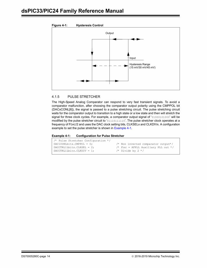
4.1.4 COMPARATOR HYSTERESIS CONTROL
The HYSSEL[1:0] bits in the DACxCONL register specify the amount of hysteresis for the analogcomparator. The HYSPOL bit specifies whether hysteresis is applied to the rising edge or fallingedge of the signal. Configuration of hysteresis helps the comparator to avoid oscillation (i.e.,toggling of the comparator output), which could be caused by noise on the positive input.
2016-2019 Microchip Technology Inc. DS70005280C-page 13
dsPIC33/PIC24 Family Reference Manual
Figure 4-1: Hysteresis Control
4.1.5 PULSE STRETCHER
The High-Speed Analog Comparator can respond to very fast transient signals. To avoid acomparator malfunction, after choosing the comparator output polarity using the CMPPOL bit(DACxCONL[6]), the signal is passed to a pulse stretching circuit. The pulse stretching circuitwaits for the comparator output to transition to a high state or a low state and then will stretch thesignal for three clock cycles. For example, a comparator output signal of ‘01000101000’ will bemodified by the pulse stretcher circuit to ‘01110111110’. The pulse stretcher clock operates at afrequency of FDAC/2 and uses the DAC clock setting bits, CLKSELx and CLKDIVx. A configurationexample to set the pulse stretcher is shown in Example 4-1.
Example 4-1: Configuration for Pulse Stretcher
Output
Input
Hysteresis Range(15 mV/30 mV/45 mV)
/* Pulse Stretcher Configuration */DAC1CONLbits.CMPPOL = 0; /* Non inverted comparator output*/DACCTRL1Lbits.CLKSEL = 2; /* FDAC = AFPLL Auxillary PLL out */DACCTRL1Lbits.CLKDIV = 1; /* Divide by 2 */
DS70005280C-page 14 2016-2019 Microchip Technology Inc.
High-Speed Analog Comparator with Slope Compensation DAC
4.1.6 DIGITAL FILTER
In many motor and power control applications, the analog comparator input signals can becorrupted by the large electromagnetic fields generated by the external switching powertransistors. Corruption of the analog input signals to the comparator can cause unwantedcomparator output transitions. A digital output filter can minimize the effects of the input signalcorruption. The digital filter processes the comparator signal from the pulse stretcher circuit.The digital filter is enabled by the FLTREN bit (DACxCONL[8]). The digital filter operates withthe clock selected by the CLKSEL[1:0] bits (DACCTRL1L[7:6]) and FCLKDIV[2:0] bits(DACCTRL1L[2:0]). The pulse stretcher output signal must be stable, either in a high state or alow state, for at least three times the selected filter clock frequency, for it to pass through the dig-ital filter. Assuming the current state is ‘0’, a comparator output string of ‘0011110000000000’ getsmodified by the pulse stretcher to ‘0011111100000000’ and to ‘0000000001111110’ by the digitalfilter if the filter clock frequency is divided by two. Because of the requirement of three similarconsecutive states for the filter, the selected digital filter clock period must be one third or lessthan the maximum desired comparator response time. In Sleep mode or Idle mode, the digitalfilter is bypassed to enable an asynchronous signal from the comparator to the interrupt con-troller. This asynchronous signal can be used to wake-up the processor from Sleep mode or Idlemode. A configuration example to enable the digital filter is provided in Example 4-2.
Example 4-2: Configuration for Digital Filter
4.2 Pulse Density Modulation (PDM) DAC
Each instance of the High-Speed Analog Comparator with Slope Compensation DAC has a ded-icated DAC that is used to program the comparator threshold voltage via the DACxDATH register.The DAC comprises a digital Pulse Density Modulation (PDM) module, followed by a multistageRC filter. The PDM module generates a high-frequency output signal whose density is propor-tional to the DACxDATH register value. The PDM module clock is selected by the CLKSEL[1:0]and CLKDIV[1:0] bits of the DACCTRL1L register. The clock selection plays an important role inthe dynamic performance of the DAC module.
The DACxDATH register value has limits of 0x0CD and 0xF32, and will provide a DAC output of5% to 95% of AVDD. For any intermediate value in the register, between 0xCD and 0xF32, theoutput voltage of the DAC will be proportional. The equation to calculate the DAC output voltage,based on the AVDD voltage source, is provided in Equation 4-1 and Register 3-6. The DAC volt-age can be varied in steps of AVDD/(2N – 1), where N is the number of DAC bits (N = 12). TheDAC modules are controlled by the DACON bit (DACCTRL1L[15]). The DACON bit enables ordisables all of the comparator modules instantiated on a given device or device core. TheDACEN bit (DACxCONL[15]) provides individual control of the DAC module. The individual DACregisters have an output enable bit, DACOEN (DACxCONL[9]), which enables the DAC outputvoltage to be routed to an external output pin, DACOUT1. The DACOUT1 pin can only be asso-ciated with a single DAC or PGA output (if available on the device) at any given time. If more thanone DACOEN bit is set, or the PGA Output Enable bit (PGAOEN) and the DACOEN bit are set,the DACOUT1 pin will be a combination of the signals. A configuration example to set the DACoutput voltage is shown in Example 4-3.
/* DAC Register Settings */DAC1DATHbits.DACDATH = 0x4D9; /* DAC Output set to 1V (AVDD = 3.3V)*/DAC1CONLbits.DACOEN = 1; /* Enable DAC 1 output on pin DACOUT1 */DAC1CONLbits.DACEN = 1; /* Enable Master DAC 1 */DACCTRL1Lbits.DACON = 1; /* Turn ON all Master DACs */
2016-2019 Microchip Technology Inc. DS70005280C-page 15
dsPIC33/PIC24 Family Reference Manual
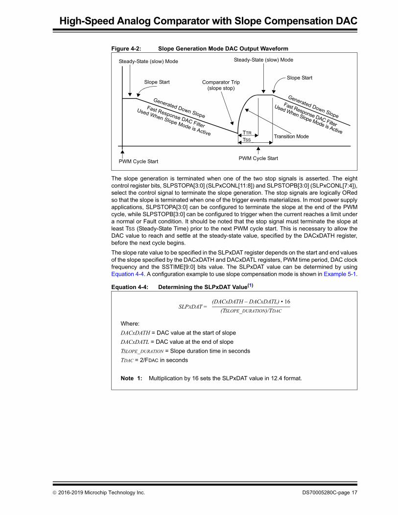
4.2.1 SLOPE GENERATOR
The function of the slope generator is to vary the DAC data value at a user-defined rate to reacha desired endpoint value. The slope generator, along with the DAC, has three modes ofoperation; namely: Slope Generation mode, Hysteretic mode and Triangle Wave mode.
4.2.1.1 Slope Generation Mode
The slope generator function can be utilized in Peak Current mode control-based power supplyapplications, where slope compensation is required. The slope function modifies the non-slopePDM DAC value repeatedly, at a user-defined rate, until the DAC data value reaches its endpoint.The slope generation function can be enabled or disabled by the SLOPEN bit (SLPxCONH[15]).The slope rate is controlled by the data in the SLPxDAT register (Register 3-10). The direction ofslope being positive or negative is controlled by the PSE bit (SLPxCONH[9]). For negative slopes(default, PSE = 0), the DACxDATH holds the nominal non-slope count, while the DACxDATL reg-ister holds the count corresponding to the end of the slope. For positive slopes (PME = 1), theDACxDATL holds the nominal non-slope count, while the DACxDATH register holds the countcorresponding to the end of the slope.
The slope generation start is controlled by the bits, SLPSTRT[3:0] (SLPxCONL[3:0]). Dependingon the value of SLPSTRT[3:0], the selected PWM trigger will be used to start the slope generation.The DAC output voltage changes to the value in the DACxDATH register first by going to theTransition mode and then to the Steady-State mode. In Transition mode, the filter responds to newdata values as fast as possible. The Transition mode duration is specified by the TMODTIME[9:0]bits (DACCTRL2L[9:0]). The source of the clock for the DAC operation is selected by bits,CLKSEL[1:0], and the frequency of operation (FDAC) is set by the divider bits, CLKDIV[1:0] of theDACCTR1L register. The Transition mode duration, TTR, is given by the equation:
Equation 4-2:
The steady-state timer, specified by the SSTIME[9:0] bits, starts at the same time as theTransition mode timer. Once the Transition mode ends, the Steady-State mode starts, whereinthe DAC output voltage settles to the new value. The Steady-State Time, TSS, is calculated bythe equation:
Equation 4-3:
Note that the SSTIME[9:0] count should always be greater than the TMODTIME[9:0] count(Figure 4-2). At the end of the Steady-State mode, the DAC value settles at the new value and isready for slope generation. The SLPSTRT[3:0] signal triggers the slope generation process.
TTR = TMODTIME[9:0] * 2/FDAC in SecondsWhere:FDAC = DAC Frequency in Hz
TSS = SSTIME[9:0] * 2/FDAC in Seconds
DS70005280C-page 16 2016-2019 Microchip Technology Inc.
High-Speed Analog Comparator with Slope Compensation DAC
The slope generation is terminated when one of the two stop signals is asserted. The eightcontrol register bits, SLPSTOPA[3:0] (SLPxCONL[11:8]) and SLPSTOPB[3:0] (SLPxCONL[7:4]),select the control signal to terminate the slope generation. The stop signals are logically ORedso that the slope is terminated when one of the trigger events materializes. In most power supplyapplications, SLPSTOPA[3:0] can be configured to terminate the slope at the end of the PWMcycle, while SLPSTOPB[3:0] can be configured to trigger when the current reaches a limit undera normal or Fault condition. It should be noted that the stop signal must terminate the slope atleast TSS (Steady-State Time) prior to the next PWM cycle start. This is necessary to allow theDAC value to reach and settle at the steady-state value, specified by the DACxDATH register,before the next cycle begins.
The slope rate value to be specified in the SLPxDAT register depends on the start and end valuesof the slope specified by the DACxDATH and DACxDATL registers, PWM time period, DAC clockfrequency and the SSTIME[9:0] bits value. The SLPxDAT value can be determined by usingEquation 4-4. A configuration example to use slope compensation mode is shown in Example 5-1.
Equation 4-4: Determining the SLPxDAT Value(1)
PWM Cycle StartPWM Cycle Start
Slope Start(slope stop)
Comparator TripSlope Start
Fast Response DAC Filter
Fast Response DAC Filter
Generated Down Slope
Generated Down SlopeUsed When Slope Mode is Active
Used When Slope Mode is Active
Steady-State (slow) Mode Steady-State (slow) Mode
Transition ModeTTR
TSS
Where:
DACxDATH = DAC value at the start of slope
DACxDATL = DAC value at the end of slope
TSLOPE_DURATION = Slope duration time in seconds
TDAC = 2/FDAC in seconds
Note 1: Multiplication by 16 sets the SLPxDAT value in 12.4 format.
(DACxDATH – DACxDATL) • 16(TSLOPE_DURATION)/TDAC
SLPXDAT =
2016-2019 Microchip Technology Inc. DS70005280C-page 17
dsPIC33/PIC24 Family Reference Manual
4.2.1.2 Hysteretic Mode
Hysteretic mode control is sometimes called “Bang-Bang” control, where a signal within a powerconverter is controlled within an upper cutoff and a lower cutoff limit. The Hysteretic mode is usedin power supply applications utilizing hysteretic control, such as LED drivers. The Hystereticmode is enabled by the HME bit (SLPxCONH[11]) and requires the SLOPEN bit to be cleared.Hysteretic Control mode enables a single DAC and comparator to monitor both the high and lowlimits for a signal. The DACxDATH register provides the higher value, while the DACxDATL reg-ister provides the lower value. When the DAC changes direction, the DAC uses Transition modeto respond and reach the new value as fast as possible. In Hysteretic mode, the comparatoreffectively functions as a window comparator. The DAC output races ahead of the monitoredvoltage in the application circuit. While the DAC is transitioning to the new value, the comparatoroutput is “blanked” via the TMCB[9:0] bits (DACxCONH[9:0]) to prevent spurious responses. Thestate of the PWM output is monitored via the input multiplexer controlled by the HCFSEL[3:0] bitsof the SLPxCONL register. This module monitors the actual state of the PWM output rather thanmake assumptions that could damage the application circuit. A configuration example to useHysteretic mode is shown in Example 5-2.
Figure 4-3: Hysteretic Mode DAC Output Waveform
PWM Cycle Start
PWM
DACxDATH
DACxDATL
PWM
Measured Application Control Signal
Comparator
Duty Cycle End
DAC Voltage
Duty Cycle
TMCBx
Cycle Restart
Counter
End
BlankingPulses
DS70005280C-page 18 2016-2019 Microchip Technology Inc.
High-Speed Analog Comparator with Slope Compensation DAC
4.2.1.3 Triangle Wave Mode
Triangle Wave mode generates an output voltage that rises and falls with a triangle wave pattern.The Triangle Wave mode is enabled by the bit, TWME (SLPxCONH[10]), and requires SLOPENto be set to ‘1’. The high and low points of the waveform are specified via the DACxDATH andDACxDATL registers. The rise and fall times, and the frequency of the triangle wave arecontrolled via the SLPxDAT register. The very first clock cycle of the slope process selects ascaled SLPxDAT value, instead of the specified value, to provide prompt DAC response to theDAC trajectory. For all subsequent clock cycles of the slope process, the slope generator usesthe specified SLPxDAT data value for incrementing/decrementing the DAC data value. The FastDAC mode is exclusive to the Triangle Wave mode and is used to provide a fast response. Theslope changes the direction automatically after reaching either the DACxDATH or DACxDATLvalue. The Triangle Wave mode is useful in digital audio applications, where an analog inputsignal is sampled via an analog comparator using a triangle wave reference signal (Figure 4-4).
Figure 4-4: Triangle Wave Mode
A configuration example to set the Triangle Wave mode is shown in Example 4-4.
Example 4-4: Triangle Wave Mode Configuration(1)
4.3 Operation in Sleep and Idle Mode
During Sleep mode, the High-Speed Analog Comparator operates with reduced functionality,allowing the device to wake-up when an active signal is applied to the comparator input. Toreduce power consumption when the device enters Idle mode, the comparator module can bedisabled by setting the DACSIDL bit (DACCTRL1L[13]). The DACSIDL bit controls all thecomparators on a device or device core.
DACxDATH
DACxDATL
0
/* Triangle Wave Mode Settings */DAC1DATLbits.DACDATL = 0x100; /* Lower data for TWM */DAC1DATHbits.DACDATH = 0xF00; /* Upper data for TWM */SLP1DATbits.SLPDAT = 0x1; /* Slope data rate */SLP1CONHbits.TWME = 1; /* Enable Triangle Mode */SLP1CONHbits.SLOPEN = 1; /* Enable Slope */
Note 1: The maximum value of DACxDATH must be set at 0xF32 – SLPxDAT and the minimum value of DACxDATL must be set at 0xCD + SLPxDAT.
2016-2019 Microchip Technology Inc. DS70005280C-page 19
dsPIC33/PIC24 Family Reference Manual
5.0 APPLICATION INFORMATION
The High-Speed Analog Comparator with Slope Compensation DAC can be used in many powerconversion applications. The outputs of the comparator module can be used to perform the followingfunctions:
• Generate an Interrupt• Trigger an ADC Sample and Convert Process• Truncate the PWM Signal (Current Limit)• Truncate the PWM Period (Current Reset)• Extend the PWM Period (Feed Forward)• Disable the PWM Outputs (Fault Latch)
The output of the comparator module can be used in multiple modes at the same time. Forexample, the comparator output can be used to generate an interrupt, have the ADC take asample and convert it, and truncate the PWM output, all in response to a voltage being detectedbeyond its expected value. The SMPS analog comparator module can also be used to wake-upthe system from Sleep mode or Idle mode when the analog input voltage exceeds the pro-grammed threshold voltage. The slope compensation module allows the user to utilize built-inhardware-based slope compensation in SMPS applications. The potential applications of thecomparator module are numerous and varied.
The following section describes typical applications of the comparator module in powerconversion circuits.
5.1 Peak Current Mode Control
The SMPS topologies, such as Buck, Boost and Buck-Boost, generate subharmonic oscillationswhen controlled with Peak Current mode control. These oscillations occur under specific condi-tions, such as Continuous Current mode and a duty cycle greater than 50%. The subharmonicoscillations can be damped by using slope compensation. The analog comparator module canbe utilized for such applications, eliminating the need for additional external analog circuitry toperform slope compensation. The comparator module is used in conjunction with the PWMmodule to generate the Current mode PWM signal. A typical Peak Current Buck mode powersupply is illustrated in Figure 5-1.
DS70005280C-page 20 2016-2019 Microchip Technology Inc.
High-Speed Analog Comparator with Slope Compensation DAC
Figure 5-1: Buck Converter with Peak Current Mode Control
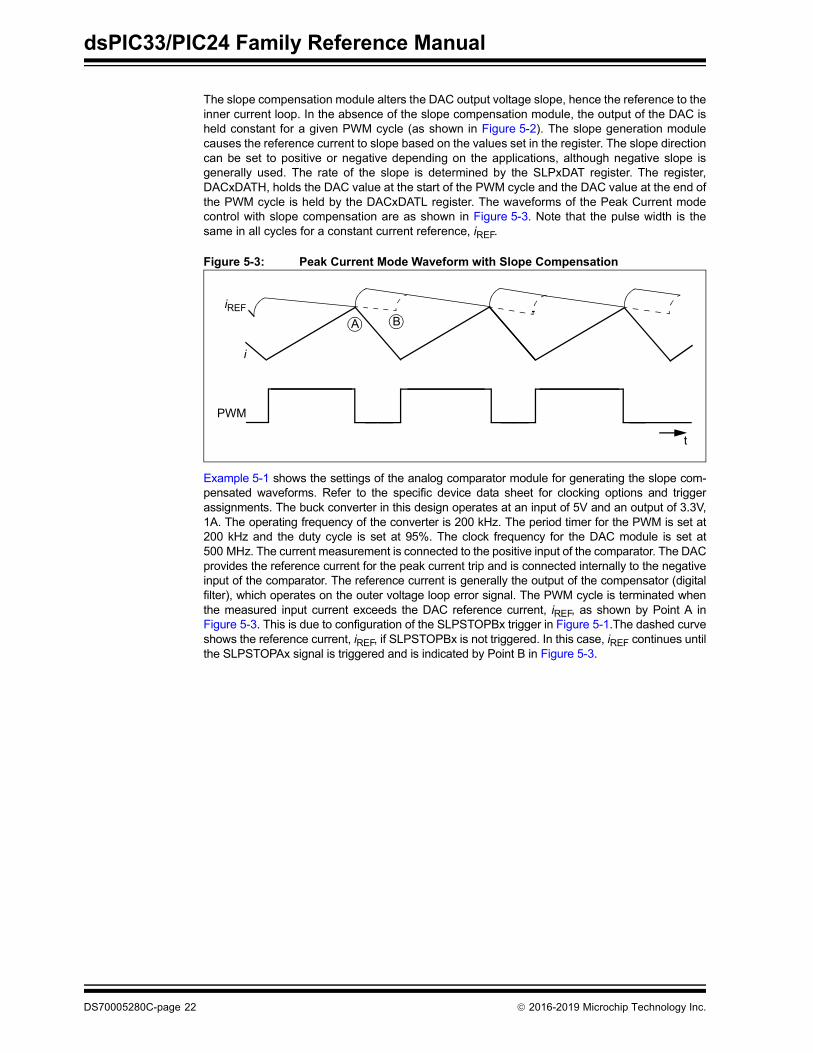
The analog comparator module is configured to reset the PWM module when the measuredinductor current peak reaches the current level determined by the outer control loop. The outercontrol loop consists of the output voltage, measured by the ADC, and compared with a desiredvoltage reference. The error counts generated are treated with a compensator gain to arrive atthe peak current level for the current PWM cycle. The peak current level is applied to the DAC togenerate an equivalent analog signal with which the actual inductor current is compared by thecomparator. The waveforms of the Peak Current mode control are as shown in Figure 5-2. Notethat the pulse width is different in the consecutive cycles, even though the current reference, iREF,is constant.
Figure 5-2: Peak Current Mode Waveform without Slope Compensation
PWM
VIN
RLOAD
VO
C
DAC
+–
–
+ADC
REF
S L
PWM
Slope
R1
D
2P2Z
PWM
R2
PWMt
iREF
i
2016-2019 Microchip Technology Inc. DS70005280C-page 21
dsPIC33/PIC24 Family Reference Manual
The slope compensation module alters the DAC output voltage slope, hence the reference to theinner current loop. In the absence of the slope compensation module, the output of the DAC isheld constant for a given PWM cycle (as shown in Figure 5-2). The slope generation modulecauses the reference current to slope based on the values set in the register. The slope directioncan be set to positive or negative depending on the applications, although negative slope isgenerally used. The rate of the slope is determined by the SLPxDAT register. The register,DACxDATH, holds the DAC value at the start of the PWM cycle and the DAC value at the end ofthe PWM cycle is held by the DACxDATL register. The waveforms of the Peak Current modecontrol with slope compensation are as shown in Figure 5-3. Note that the pulse width is thesame in all cycles for a constant current reference, iREF.
Figure 5-3: Peak Current Mode Waveform with Slope Compensation
Example 5-1 shows the settings of the analog comparator module for generating the slope com-pensated waveforms. Refer to the specific device data sheet for clocking options and triggerassignments. The buck converter in this design operates at an input of 5V and an output of 3.3V,1A. The operating frequency of the converter is 200 kHz. The period timer for the PWM is set at200 kHz and the duty cycle is set at 95%. The clock frequency for the DAC module is set at500 MHz. The current measurement is connected to the positive input of the comparator. The DACprovides the reference current for the peak current trip and is connected internally to the negativeinput of the comparator. The reference current is generally the output of the compensator (digitalfilter), which operates on the outer voltage loop error signal. The PWM cycle is terminated whenthe measured input current exceeds the DAC reference current, iREF, as shown by Point A inFigure 5-3. This is due to configuration of the SLPSTOPBx trigger in Figure 5-1.The dashed curveshows the reference current, iREF, if SLPSTOPBx is not triggered. In this case, iREF continues untilthe SLPSTOPAx signal is triggered and is indicated by Point B in Figure 5-3.
PWM
t
iREF
i
A B
DS70005280C-page 22 2016-2019 Microchip Technology Inc.
High-Speed Analog Comparator with Slope Compensation DAC
Example 5-1: Initialize DAC with Slope Compensation
// PWM Configuration PCLKCONbits.MCLKSEL = 1; // AFVCO/2 as clock source (500 Mhz) PG1CONLbits.CLKSEL = 1; // Clock selected by MCLKSEL PG1PER = 2499; // PWM frequency is 200 kHz, 5 uS period PG1DC = 2375; // 95% duty cycle, 4.75 uS on time PG1IOCONHbits.PENH = 1; // PWM Generator controls the PWMxH output pin PG1IOCONHbits.PENL = 1; // PWM Generator controls the PWMxL output pin // PWM PCI setup, use CLDAT when comparator 1 trips PG1CLPCILbits.PSS = 27; // PCI source is Comparator 1 PG1CLPCILbits.AQSS = 2; // LEB active as Acceptance Qualifier PG1CLPCILbits.AQPS = 1; // Invert Acceptance Qualifier (LEB not active) PG1CLPCILbits.TERM = 1; // Auto terminate as Termination Event PG1CLPCIHbits.ACP = 3; // Latched PCI Acceptance Criteria PG1IOCONLbits.CLDAT = 0b01; // PWM1L = 1 and PWM1H = 0 if CL event is active PG1LEBHbits.PHR = 1; // Rising edge of PWMxH triggers the LEB counter PG1LEBL = 30; // 500 nS LEB timer // PWM to DAC Trigger setup PG1TRIGA = 750; // ADC Trigger 1 at 1.5 uS, used as SLPSTRT PG1EVTLbits.ADTR1EN1 = 1; // PGxTRIGA as trigger source for ADC Trigger 1 PG1TRIGB = 2000; // ADC Trigger 2 at 4 uS, used as SLPSTOPA PG1EVTHbits.ADTR2EN2 = 1; // PGxTRIGB as trigger source for ADC Trigger 2 PG1CONLbits.ON = 1; // Enable PWM // DAC Configuration DACCTRL1Lbits.CLKSEL = 0; // AFVCO/2 as clock source (500 Mhz) DACCTRL2Hbits.SSTIME = 0x8A; // Default value 552 nS @ 500MHz DACCTRL2Lbits.TMODTIME = 0x55; // Default value 340 nS @ 500MHz DAC1DATHbits.DACDATH = 2703; // 2.17v steady state value DAC1DATLbits.DACDATL = 1113; // 0.89v, value at the end slope SLP1DATbits.SLPDAT = 41; // Slope = (2703-1113)*16/((4u-1.5u)/4n) SLP1CONHbits.SLOPEN = 1; // Enable Slope compensation SLP1CONLbits.SLPSTRT = 1; // PWM1 ADC Trigger 1 SLP1CONLbits.SLPSTOPA = 1; // PWM1 ADC Trigger 2 SLP1CONLbits.SLPSTOPB = 1; // Comparator 1 DAC1CONHbits.TMCB = 125; // 125 * 4 nS = 500 nS blanking time DAC1CONLbits.DACOEN = 1; // Enable DAC output DAC1CONLbits.DACEN = 1; // Enable DAC 1 DACCTRL1Lbits.DACON = 1; // Enable DAC system
2016-2019 Microchip Technology Inc. DS70005280C-page 23
dsPIC33/PIC24 Family Reference Manual
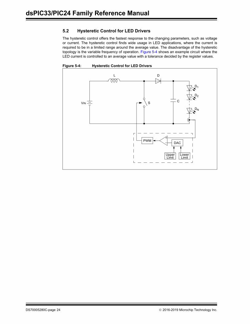
5.2 Hysteretic Control for LED Drivers
The hysteretic control offers the fastest response to the changing parameters, such as voltageor current. The hysteretic control finds wide usage in LED applications, where the current isrequired to be in a limited range around the average value. The disadvantage of the hysteretictopology is the variable frequency of operation. Figure 5-4 shows an example circuit where theLED current is controlled to an average value with a tolerance decided by the register values.
Figure 5-4: Hysteretic Control for LED Drivers
VINC
+
– DAC
Upper
L D
S
D1
D2
DN
LimitLowerLimit
PWM
DS70005280C-page 24 2016-2019 Microchip Technology Inc.
High-Speed Analog Comparator with Slope Compensation DAC
The comparator uses Hysteretic mode for such applications. The Hysteretic mode is controlledby the HME bit in the SLPxCONH register. In order to enable the Hysteretic mode, the HME bitmust be set to ‘1’ and the SLOPEN bit is cleared. The upper limit of the hysteretic control isdefined by the DACxDATH register, while the lower limit is defined by the DACxDATL register. InHysteretic mode, the comparator module has a pair of output signals that are available asPeripheral Pin Select (PPS) inputs: PWM_Req_on and PWM_Req_off. These signals can thenbe mapped to the PWM PCI input for controlling the PWM outputs. The DAC settings forHysteretic mode are shown in Example 5-2. Refer to the specific device data sheet for clockingoptions and trigger assignments.
Example 5-2: DAC Settings for Hysteretic Mode
5.3 Using DAC as Voltage Reference for External Comparator
If the DAC output is used as a reference voltage for a comparator external to the dsPIC33 device,the Transition mode’s transient response can cause unwanted comparator trips when changingDACDATx values. When the DAC is in Transition mode, the blanking feature (CBE = 1) can beset to mask the internal comparator’s output. However, this blanking feature is not available onan external comparator.
A work around for this use case is to set the TMODTIME[9:0] bits in the DACCTRL2L register tozero to disable Transition mode. The DAC will slew slower to the new target voltage.
2016-2019 Microchip Technology Inc. DS70005280C-page 25
dsPIC33/PIC24 Family Reference Manual
6.0 LIMITATIONS
6.1 Comparator Input Range
The High-Speed Analog Comparator with Slope Compensation DAC has a limitation for the inputCommon-Mode Range (CMR) to not exceed (AVDD + 0.2V). This means that the input to thecomparator (the selected CMPx input pin) should be within this range. As long as the input iswithin the CMR, the comparator output will be correct. Any input exceeding the CMR limitationwill cause the comparator input to be saturated.
DS70005280C-page 26 2016-2019 Microchip Technology Inc.
High-Speed Analog Comparator with Slope Compensation DAC
7.0 RELATED APPLICATION NOTES
This section lists application notes that are related to this section of the manual. These applicationnotes may not be written specifically for the dsPIC33/PIC24 device families, but the concepts arepertinent and could be used with modification and possible limitations. The current applicationnotes related to the High-Speed Analog Comparator with Slope Compensation DAC are:
Title Application Note #
No related application notes at this time. N/A
Note: Please visit the Microchip website (www.microchip.com) for additional applicationnotes and code examples for the dsPIC33/PIC24 families of devices.
2016-2019 Microchip Technology Inc. DS70005280C-page 27
Updates the document title from High-Speed Analog Comparator Module to High-Speed AnalogComparator with Slope Compensation DAC.
Minor grammatical and formatting changes throughout the document.
DS70005280C-page 28 2016-2019 Microchip Technology Inc.
Note the following details of the code protection feature on Microchip devices:
• Microchip products meet the specification contained in their particular Microchip Data Sheet.
• Microchip believes that its family of products is one of the most secure families of its kind on the market today, when used in the intended manner and under normal conditions.
• There are dishonest and possibly illegal methods used to breach the code protection feature. All of these methods, to our knowledge, require using the Microchip products in a manner outside the operating specifications contained in Microchip’s Data Sheets. Most likely, the person doing so is engaged in theft of intellectual property.
• Microchip is willing to work with the customer who is concerned about the integrity of their code.
• Neither Microchip nor any other semiconductor manufacturer can guarantee the security of their code. Code protection does not mean that we are guaranteeing the product as “unbreakable.”
Code protection is constantly evolving. We at Microchip are committed to continuously improving the code protection features of ourproducts. Attempts to break Microchip’s code protection feature may be a violation of the Digital Millennium Copyright Act. If such actsallow unauthorized access to your software or other copyrighted work, you may have a right to sue for relief under that Act.
Information contained in this publication regarding deviceapplications and the like is provided only for your convenienceand may be superseded by updates. It is your responsibility toensure that your application meets with your specifications.MICROCHIP MAKES NO REPRESENTATIONS ORWARRANTIES OF ANY KIND WHETHER EXPRESS ORIMPLIED, WRITTEN OR ORAL, STATUTORY OROTHERWISE, RELATED TO THE INFORMATION,INCLUDING BUT NOT LIMITED TO ITS CONDITION,QUALITY, PERFORMANCE, MERCHANTABILITY ORFITNESS FOR PURPOSE. Microchip disclaims all liabilityarising from this information and its use. Use of Microchipdevices in life support and/or safety applications is entirely atthe buyer’s risk, and the buyer agrees to defend, indemnify andhold harmless Microchip from any and all damages, claims,suits, or expenses resulting from such use. No licenses areconveyed, implicitly or otherwise, under any Microchipintellectual property rights unless otherwise stated.
2016-2019 Microchip Technology Inc.
For information regarding Microchip’s Quality Management Systems, please visit www.microchip.com/quality.
TrademarksThe Microchip name and logo, the Microchip logo, Adaptec, AnyRate, AVR, AVR logo, AVR Freaks, BesTime, BitCloud, chipKIT, chipKIT logo, CryptoMemory, CryptoRF, dsPIC, FlashFlex, flexPWR, HELDO, IGLOO, JukeBlox, KeeLoq, Kleer, LANCheck, LinkMD, maXStylus, maXTouch, MediaLB, megaAVR, Microsemi, Microsemi logo, MOST, MOST logo, MPLAB, OptoLyzer, PackeTime, PIC, picoPower, PICSTART, PIC32 logo, PolarFire, Prochip Designer, QTouch, SAM-BA, SenGenuity, SpyNIC, SST, SST Logo, SuperFlash, Symmetricom, SyncServer, Tachyon, TempTrackr, TimeSource, tinyAVR, UNI/O, Vectron, and XMEGA are registered trademarks of Microchip Technology Incorporated in the U.S.A. and other countries.
APT, ClockWorks, The Embedded Control Solutions Company, EtherSynch, FlashTec, Hyper Speed Control, HyperLight Load, IntelliMOS, Libero, motorBench, mTouch, Powermite 3, Precision Edge, ProASIC, ProASIC Plus, ProASIC Plus logo, Quiet-Wire, SmartFusion, SyncWorld, Temux, TimeCesium, TimeHub, TimePictra, TimeProvider, Vite, WinPath, and ZL are registered trademarks of Microchip Technology Incorporated in the U.S.A.
Adjacent Key Suppression, AKS, Analog-for-the-Digital Age, Any Capacitor, AnyIn, AnyOut, BlueSky, BodyCom, CodeGuard, CryptoAuthentication, CryptoAutomotive, CryptoCompanion, CryptoController, dsPICDEM, dsPICDEM.net, Dynamic Average Matching, DAM, ECAN, EtherGREEN, In-Circuit Serial Programming, ICSP, INICnet, Inter-Chip Connectivity, JitterBlocker, KleerNet, KleerNet logo, memBrain, Mindi, MiWi, MPASM, MPF, MPLAB Certified logo, MPLIB, MPLINK, MultiTRAK, NetDetach, Omniscient Code Generation, PICDEM, PICDEM.net, PICkit, PICtail, PowerSmart, PureSilicon, QMatrix, REAL ICE, Ripple Blocker, SAM-ICE, Serial Quad I/O, SMART-I.S., SQI, SuperSwitcher, SuperSwitcher II, Total Endurance, TSHARC, USBCheck, VariSense, ViewSpan, WiperLock, Wireless DNA, and ZENA are trademarks of Microchip Technology Incorporated in the U.S.A. and other countries.
SQTP is a service mark of Microchip Technology Incorporated in the U.S.A.The Adaptec logo, Frequency on Demand, Silicon Storage Technology, and Symmcom are registered trademarks of Microchip Technology Inc. in other countries.GestIC is a registered trademark of Microchip Technology Germany II GmbH & Co. KG, a subsidiary of Microchip Technology Inc., in other countries. All other trademarks mentioned herein are property of their respective companies.