Page 1
U.P.B. Sci. Bull., Series C, Vol. 83, Iss. 1, 2021 ISSN 2286-3540
DSSS-DRMC BASED SECURE TRANSMISSION WITH FPGA
IMPLEMENTATION
Hamsa A. ABDULLAH1, Raya K. MOHAMMED
2
In Direct Sequence Spread Spectrum (DSSS), the information signal is
denoted by a spreading signal over a band that is much larger than the original
bandwidth, the main advantage of DSSS technique is to provide more security to the
transmitted signal. In this paper, new structures are proposed and implemented to
enhance transmission’s security over traditional DSSS, while the Field Programmable Gate Array (FPGA) implementation of DSSS-based communication
system is considered. The proposed techniques used different random multiple codes
(DRMC) in DSSS, the spreading code with the size of 11 bits is used as single,
double and triple bits sequence. The MATLAB-based simulated results of DSSS-
DRMC show that the spreading and modulated signals look like noise. The standard
DSSS system with baseband transmission is implemented in FPGA hardware using
System Generator, Vivado 2017.4, NEXYS 4 DDR board with ARTIX 7 XC7A100T.
The device utilization results show that the DSP % used in single bit DSSS is
23.75%, while the bounded IO is 20.48%.
Keywords: FPGA, DSSS, Security, DRMC, Vivado, System Generator
1. Introduction
The performance of wireless communications is enhanced by eliminating
the multipath fading and interference from channel [1]. In spread spectrum (SS)
transmission, the transmitted signal takes more bandwidth, the bandwidth of
spreading is determined by the sequence which is independent of data bandwidth
[2]. SS has various methods such as Time Hopping Spread Spectrum (THSS),
Frequency Hopping Spread Spectrum (FHSS), DSSS and a combination of these
methods. The main advantages of SS are security, low probability of intercept,
resolution ranging, Code Division Multiple Access (CDMA), anti-jamming and
high anti-interference [3, 4]. At the receiver, the received spread signal is used to
recover the original signal by using the same procedure but in reverse [5, 6, 7].
In DSSS, the modulated signal is spread with bandwidth larger than the
original information signal bandwidth. At the transmitter, the DSSS technique
1 College of Information Engineering, Al-Nahrain University, Iraq,
E-mail: [email protected] 2 College of Information Engineering, Al-Nahrain University, Iraq,
E-mail: [email protected]
Page 2
148 Hamsa A. Abdullah, Raya K. Mohammed
reduce the signal’s interference, while at the receiver, it helps to recover the
original data if data bits are damaged during transmission [8, 9].
In [10], secure data transmission based on FHSS and DSSS was designed
and implemented is introduced. This work mostly concerns the design of SS
techniques, mainly DSSS and FHSS. In [11], Two SS based wireless video
transmission schemes performance comparison is presented. In this work, the
proposed schemes are designed and implemented based on spread spectrum
technique. These schemes are DSSS and multi-code SS (MCSS). The software
defined radio (SDR) technique is used to implement two schemes. The XILINX
Virtex-4 FPGA used to implement the transmitter while Virtex-5 FPGA used to
implement the receiver.
In [12], implementation of DSSS communication system using FPGA is
introduced. This work introduces the design and implementation of SS techniques
to defeat the interference problems. In [13], Code Tracking of DSSS over AWGN
Channel is presented. In this paper, MATLAB simulator is used to prove the
synchronization of code clock between transmitter and receiver. In [14],
Development of Multi-user TDMA based DSSS system is introduced. In this
paper, a complete frame structure of hybrid system based on TDMA DSSS is
designed and implemented by using MATLAB. In [15], Implementation of BPSK,
DSSS and DQPSK Modulators and their Performance Comparison in VHDL is
introduced. In this work, DSSS modulator, BPSK Modulator and Differential
QPSK Modulator are designed to enhance the security and improve the capacity.
The performance of these three modulation techniques is compared in terms of
area and power. The entire design is done in XILINX ISE 14.5 software using
VHDL. The device used is VIRTEX4 starter kit.
There are two main contributions in this paper, the first contribution is the
design of DSSS – based enhancement security transmission method. This method
is called (DSSS-DRMC). It uses N spreading codes (N=1, 2, 3) to spread the
message signal with different bits length (single, double, or triple) over larger
bandwidth. The method insures a more secure system as comparing with existing
ones since it based on DRMC method which also can be worked with BPSK
system. The second contribution is the implementation of a DSSS-based
communication system in FPGA hardware. The high-speed parallel processing of
FPGA is used to realize the sophisticated processing of wide bandwidth DSSS
signals.
2. Research Method
In this work, efforts are paid to develop a new method of DSSS to increase
the security level and data rate transmission over wireless communication. The
initial motivation was to design a new method based on Multi Code-DSSS. The
Page 3
DSSS-DRMC based secure transmission with FPGA implementation 149
new method called as DSSS with Different Random Multiple Codes (DSSS-
DRMC). DSSS-DRMC uses N spreading codes (N=1, 2, 3) to spread the message
signal with different bits length (single, double, or triple) over larger bandwidth.
By using multiple spreading codes for different data packets, the transmission
security can be enhanced. The security level is affected directly by the number of
spreading codes, where there is no correlation between these used codes. In
DSSS-DRMC, the spreading code that used to spread the information bits is
selected randomly. So, the unauthorized user cannot determine which codes that
used to spread the information bits. The block diagram of DSSS-DRMC shown in
Fig. 1.
Fig. 1 DSSS-DRMC
2.1 Single Bit DSSS-DRMC
The transmission of Single Bit DSSS-DRMC method use 2 SS codes. At
the transmitter, data packet (1 bit) is replaced by one out of two SS codes for
information spreading based on switch operation as shown in Eq.1. After
spreading the signal packet, the BPSK modulator process the spreading signal
before the transmission.
(1)
2.2 Double Bit DSSS-RSMC
The transmission of Double Bit DSSS-DRMC method use 4 SS codes. At
the transmitter, data packet (2 bit) is replaced by one out of four SS codes for
information spreading based on switch operation as shown in Eq.2. As in previous
method, the BPSK system is used to modulate the spreading signal before the
transmission.
Page 4
150 Hamsa A. Abdullah, Raya K. Mohammed
(2)
2.3 Triple Bit DSSS-RSMC
The transmission of triple Bit DSSS-DRMC method use 8 SS codes. At
the transmitter, data packet (3 bit) is replaced by one out of eight SS codes for
information spreading based on switch operation as shown in Eq.3. The BPSK
system is also used to modulate the spreading signal before the transmission.
(3)
In addition, a secure communication system is implemented in FPGA. The
system consists of transmitter and receiver. The transmitter contains a Single Bit
DSSS and PSK Modulator while the receiver contains a PSK Demodulator and
De-speared system.
3. Results and analysis
In this paper, the results are shown in two-stage: simulation results
(MATLAB) and hardware results (system generator and FPGA device).
3.1 Simulation Results
All the proposed methods (single, double and triple) bit DSSS-DRMC are
implemented in MATLAB environment. Firstly, the binary information is spread
based on using the proposed methods where the length of SS is 11 bits as shown
in Fig. 2.
Secondly, the spread signals are processed to PSK modulator and PSK
demodulator and the results are shown in Fig.2. The results show that the DSSS-
DRMC and modulated signals look like noise.
For system performance evaluation, the correlation is measured for all
methods and the results (Fig. 3) show that the autocorrelation peaks are appeared
Page 5
DSSS-DRMC based secure transmission with FPGA implementation 151
at 0. PAPR and signal power measurement are used to evaluate the performance
of the proposed system compared with Ref [11].
PAPR has significantly important effects in communication system. The
high value of PAPR is leading to a decrease in the power amplifier efficiency at
the transmitter [11]. The result of PAPA in Table 1 shows that the proposed
system has better performance than the performance of Ref. [11].
(a) (b)
(c)
Fig. 2: The spreading of DSSS- DRMC (a) Single Bit (b) Double Bit (c) Triple Bit
Table 1 shows that the spreading operation of the proposed system will
generate processing gain more efficient than Ref. [11].
Page 6
152 Hamsa A. Abdullah, Raya K. Mohammed
Table 1
Comparison of the Performance Evaluation
Scheme PAPR (dB) The measured signal
power (dBm)
Proposed System 3.0103 -26.9897
Ref [11] 7.3 -19.5
(a) (b)
(c)
Fig. 3: The Spectrum of DSSS- DRMC (a) Single Bit (b) Double Bit (c) Triple Bit
3.2 Hardware results
In this paper, DSSS system is implemented in FPGA hardware using
system generator tool. With the high-speed parallel processing of FPGA platform,
the developed processing of wide bandwidth DSSS signals can be realized. In
Page 7
DSSS-DRMC based secure transmission with FPGA implementation 153
addition, the application will be flexible, more secure to interference in the
wideband domain of DSSS system.
System Generator is an efficient tool to design, test & implement high
performance algorithms on Xilinx devices. The designing of communication
systems using this tool, takes advantages of both simulation and hardware
environments. The hardware design of transmitting and receiving data by using
DSSS is shown in Fig. 4.
Fig. 4 The Design of single bit DSSS system using System Generator
The system consists of four stages: Single Bit DSSS, PSK Modulator, PSK
Demodulator, and De-speared Spectrum. Each stage is represented by a
subsystem. The input signals to the SS system (Input message and PN sequence)
are generated using LFSR blocks. These blocks are internal inputs in system
generator environment, so it’s not required to use gateway-in blocks in this case.
And this can reduce the hardware cost in FPGA environment. The main output
signals are connected to oscilloscope (scop4 in Fig. 4). Fig. 5 shows the output
waveform the proposed system.
Fig. 5. The output waveform of the proposed system
Page 8
154 Hamsa A. Abdullah, Raya K. Mohammed
The waveform results are: the message signal, the spread signal,
modulated signal, demodulated signal of and recovered signal. The last waveform
signal proved that the transmitted message signal can be recovered successfully at
the receiver.
3.2.1 Hardware implementation of Single Bit DSSS Transmission
As shown in Fig. 6a, the design of single bit DSSS is implemented using
system generator blocks.
(a) (b)
Fig. 6: Single bit DSSS transmission subsystem (a) The design system. (b) The output waveform
In this implementation, the used blocks are: Unipolar to polar (using
ROM), Multiplier, Constant, Rational, output gateway and scope. Since its
necessary to convert the binary unipolar message to polar before spreading, the
main input message and the PN sequence are processed to ROM blocks with
appropriate settings for this purpose.
In the opposite side, relational blocks are used to convert polar to unipolar.
The input message, PN sequence and the output speared signal are connected to
oscilloscope, and the outputs waveforms of these signals are shown in Fig. 6b.
The waveforms output proved that the spreading operation is performed
successfully.
Page 9
DSSS-DRMC based secure transmission with FPGA implementation 155
3.2.2 Hardware implementation of BPSK Modulator
As shown in Fig. 7a, the design of PSK modulator is implemented by
using system generator blocks. In this implementation, the blocks that used are:
Multiplexor, input gateway, output gateway and Scope.
(a) (b)
Fig. 7: BPSK modulator subsystem (a) The design system (b) The output waveform
An external sinewave input block and a gain block of (-1) are used to
perform the PSK modulation (as shown in Fig. 8).
Fig. 8: BPSK demodulator subsystem (a) The design system
Page 10
156 Hamsa A. Abdullah, Raya K. Mohammed
(a) (b)
Fig. 8: BPSK demodulator subsystem (b) The output waveform
The output of these blocks is connected to In2 and In3 of PSK subsystem
as shown in Fig. 7a. The speared signal and the PSK modulated signal are
connected to an oscilloscope, and the waveform outputs are shown in Fig.7b.
3.2.3 Hardware implementation of BPSK De-Modulator
As shown in Fig. 8a, the design of PSK de-modulator is implemented by
using system generator blocks. In this implementation, the used blocks are:
Multiplier, Constant, Rational, Digital FIR Filter, input gateway, output gateway
and Scope. The relational block is used to perform the de-multiplexing operation.
The FDA Tool are used to determine the coefficients that had been inserted in the
Digital FIR filter block. The modulated signal is connected to In1 in PSK
demodulator subsystem while the sine wave input is connected to In2. These two
signals are multiplied to perform the demodulation process. The modulated signal
and the demodulated signal are connected to an oscilloscope, and the waveform
outputs are shown in Fig. 8b.
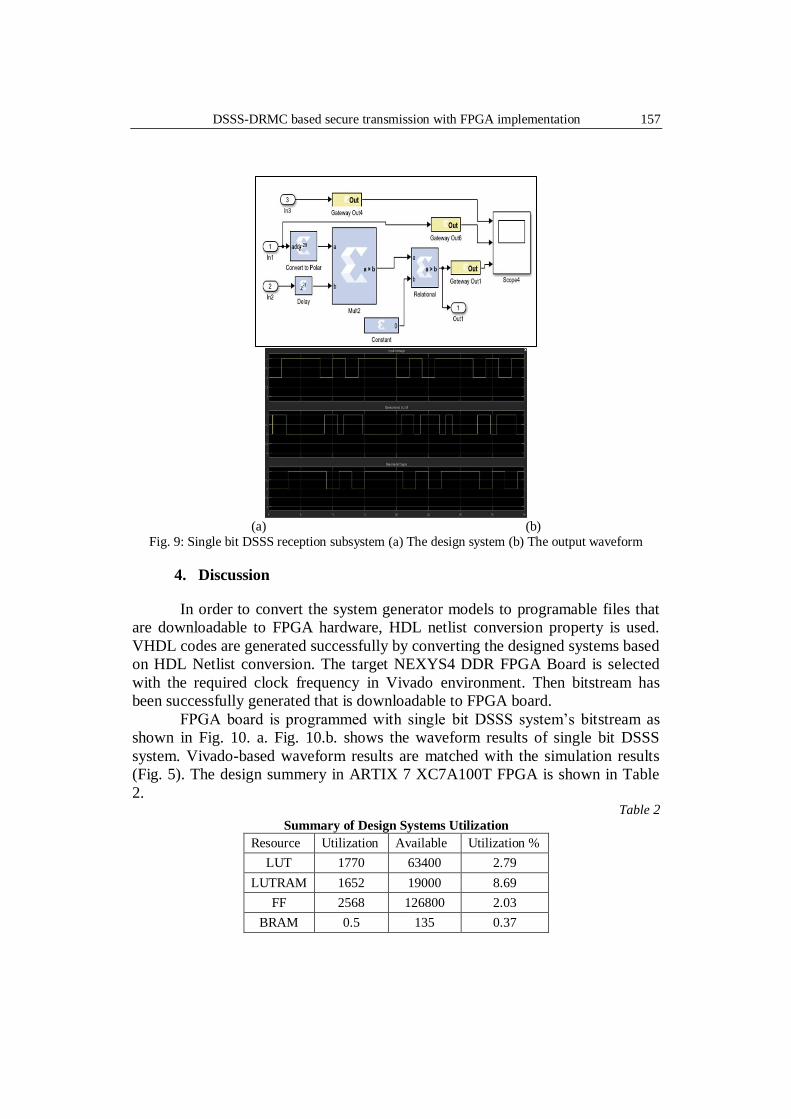
3.2.4 Hardware implementation of Single Bit De-Speared Spectrum
As shown in Fig. 9, the design of Single Bit De-DSSS is implemented
using system generator blocks. In this implementation, the blocks that used are:
Multiplier, Constant, Rational, Delay, ROM, output gateway, and Scope. The
latency value in ROM block and the delay block are used for synchronization
between SS (PN sequence) and the received signal. The demodulated signal is
connected to In1, the PN sequence signal is connected to In2, while the input
message is connected to In3 in de-spreading subsystem as shown in Fig. 4. The
Input message, demodulated signal and the reconstructed signal are connected to
an oscilloscope, and the waveform outputs are shown in Fig. 9b. the output
waveforms proved that the transmitted signal are reconstructed successfully.
Page 11
DSSS-DRMC based secure transmission with FPGA implementation 157
(a) (b)
Fig. 9: Single bit DSSS reception subsystem (a) The design system (b) The output waveform
4. Discussion
In order to convert the system generator models to programable files that
are downloadable to FPGA hardware, HDL netlist conversion property is used.
VHDL codes are generated successfully by converting the designed systems based
on HDL Netlist conversion. The target NEXYS4 DDR FPGA Board is selected
with the required clock frequency in Vivado environment. Then bitstream has
been successfully generated that is downloadable to FPGA board.
FPGA board is programmed with single bit DSSS system’s bitstream as
shown in Fig. 10. a. Fig. 10.b. shows the waveform results of single bit DSSS
system. Vivado-based waveform results are matched with the simulation results
(Fig. 5). The design summery in ARTIX 7 XC7A100T FPGA is shown in Table
2. Table 2
Summary of Design Systems Utilization
Resource Utilization Available Utilization %
LUT 1770 63400 2.79
LUTRAM 1652 19000 8.69
FF 2568 126800 2.03
BRAM 0.5 135 0.37
Page 12
158 Hamsa A. Abdullah, Raya K. Mohammed
DSP 57 240 23.75
IO 43 210 20.48
Fig. 10 FPGA Programing Board (a) DSSS Bitstream (b) DSSS Waveform Results
These resources are LUT, LUTRAM, FF, BRAM, DSP, and IO blocks
number. The table show the LUT utilization % that used in single bit DSSS is
2.79%. And also, the Bounded IO that used is 20.48%. Both the MATLAB
simulation and FPGA hardware results show that, the transmitted signal has been
successfully reconstructed at the receiver.
5. Conclusions
In this work, the design of new proposed techniques of DSSS-DRMC are
presented. The proposed techniques depend on the number of bits that represented
by spreading sequence. The transmission security is enhanced by using the
proposed techniques where the security level is affected directly by the number of
spreading codes. All three proposed techniques simulated via MATLAB
program. The simulation results show that, the spreading and modulated signal
look like noise. The Single Bit DSSS system is implemented in hardware using
system generator, Vivado 2017.4 and NEXYS 4 ARTIX 7 DDR FPGA board.
The FPGA implementation add another security level to the system in terms of
minimizing the processing time and enhanced the flexibility. The results show that
Page 13
DSSS-DRMC based secure transmission with FPGA implementation 159
the deigned system utilized lower possible available numbers of resources in
targeted device.
R E F E R E N C E S
[1] N. Motlagh, "Frequency Hopping Spread Spectrum: An Effective Way to Improve Wireless
Communication Performance," in Advanced Trends in Wireless Communications , BoD–
Books on Demand, 2011, pp. 187-202.
[2] B. S. Devi, J.L.Jini, G.M. Bell, "Comparative Analysis of Direct Sequence Spread Spectrum
using Rabbit Stream Cipher," International Journal of Advanced Research in Electronics and
Communication Engineering (IJARECE), vol. 5, no. 10, pp. 2373-2379, 2016.
[3] S. Latif, M. Kamran, W. Din, R. Ullah and A. Nouman , "Security Enhancement of Fhss
Transmission System Using Hopping Sequence and its Compliment (CHS-FHSS)," World
Applied Sciences Journal, vol. 21, no. 6, pp. 920-926, 2013.
[4] C. Popper, M. Strasser, and S. Capkun, "Anti-jamming Broadcast Communication using
Uncoordinated Spread Spectrum Techniques," IEEE Journal on Selected Areas in
Communications, vol. 28, no. 5, pp. 1-13, 2010.
[5] J. Rajesh, M. Tech, K. Babu, "Design of Multiuser CDMA Systems in Fading Channels," Int.
J. Comp. Tech. Appl, vol. 2, no. 5, pp. 1600-1617, 2011.
[6] M. P. Chawla, M.Tech, "A Review Comparison of different Spreading Codes for DS
CDMA," International Journal for Scientific Research & Development, vol. 2, no. 2, pp. 995-
999, 2014.
[7] R.Mohammed, H. Abdullah, "Implementation of Digital and Analog Modulation Systems
using FPGA," Indonesian Journal of Electrical Engineering and Computer Science, vol. 18,
no. 1, pp. 485-493, 2020.
[8] S. Latif and R. Ullah, "Random Selection of Multiple Spreading Codes Enhances the Security
of DSSS Transmission (RSMC-DSSS)," International Journal of Security and Its
Applications, vol. 7, no. 3, pp. 377-386, 2013.
[9] K. Harman, A. Caldow, C. Potter, J. Arnold and G. Parker, "A Wideband FPGA-Based
Digital DSSS," in Signal Processing for Telecommunications and Multimedia,Multimedia
Systems and Applications Series, Boston, MA, vol. 27, Springer, 2005, pp. 249-268.
[10] M. Hasan, J. M. Thakur, and P. Podder, "Design and Implementation of FHSS and DSSS for
Secure Data Transmission," International Journal of Signal Processing Systems, vol. 4, no. 2,
pp. 144-149, 2016.
[11] Z. Zhang, F. Tian, F. Zeng, S. He, Y. Liu, G. Xuan, "Performance Comparison of Two
Spread-Spectrum- Based Wireless Video Transmission Schemes," in 9th International
Congress on Image and Signal Processing, BioMedical Engineering and Informatics(CISP-
BME), Datong, China, 2016.
[12] R.Prabhu, R.Nagarajan, N.Karthick, S.Suresh, "Implementation of Direct Sequence Spread
Spectrum Communication System Using FPGA," International Journal of Advanced
Engineering, Management and Science (IJAEMS), vol. 3, no. 5, pp. 488-496, 2017.
[13] M. Abdulhamed, H. Omer, "Code Tracking of DSSS over AWGN Channel," Scientific
Bulletin of the Electrical Engineering Faculty, vol. 40, no. 1, 2019.
Page 14
160 Hamsa A. Abdullah, Raya K. Mohammed
[14] A. Sajid , A. Habib , S. Ali , S. Ejaz, "Development of multi-user TDMA-based DSSS
system," in 2nd International conference on Communication, Computer, Digital Systems (C-
CODE).IEEE, Islamabad, Pakistan, Pakistan, 2019.
[15] S Rao, N. Lakshmi, V. Geetanjali, "Implementation of BPSK, DSSS and DQPSK Modulators
and their Performance Comparison in VHDL”,," International Journal of Innovative
Technology and Exploring Engineering (IJITEE), vol. 8, no. 6, 2019.