146
DT9847 Series UM-24847-L User’s Manual Title Page

DT9847 Series
UM-24847-L
User’s Manual
Title Page

Copyright Page
Trademark and Copyright Information
Measurement Computing Corporation, InstaCal, Universal Library, and the Measurement Computing logo are either trademarks or registered trademarks of Measurement Computing Corporation. Refer to the Copyrights & Trademarks section on mccdaq.com/legal for more information about Measurement Computing trademarks.
Other product and company names mentioned herein are trademarks or trade names of their respective companies.
© 2019 Measurement Computing Corporation. All rights reserved. No part of this publication may be reproduced, stored in a retrieval system, or transmitted, in any form by any means, electronic, mechanical, by photocopying, recording, or otherwise without the prior written permission of Measurement Computing Corporation.
Notice
Measurement Computing Corporation does not authorize any Measurement Computing Corporation product for use in life support systems and/or devices without prior written consent from Measurement Computing Corporation. Life support devices/systems are devices or systems that, a) are intended for surgical implantation into the body, or b) support or sustain life and whose failure to perform can be reasonably expected to result in injury. Measurement Computing Corporation products are not designed with the components required, and are not subject to the testing required to ensure a level of reliability suitable for the treatment and diagnosis of people.
FCC Page
Radio and Television Interference
This equipment has been tested and found to comply with CISPR EN55022 Class A and EN61000-6-1 requirements and also with the limits for a Class A digital device, pursuant to Part 15 of the FCC Rules. These limits are designed to provide reasonable protection against harmful interference when the equipment is operated in a commercial environment. This equipment generates, uses, and can radiate radio frequency energy and, if not installed and used in accordance with the instruction manual, may cause harmful interference to radio communications. Operation of this equipment in a residential area is likely to cause harmful interference, in which case the user will be required to correct the interference at his own expense.
Changes or modifications to this equipment not expressly approved by Data Translation could void your authority to operate the equipment under Part 15 of the FCC Rules.
Note: This product was verified to meet FCC requirements under test conditions that included use of shielded cables and connectors between system components. It is important that you use shielded cables and connectors to reduce the possibility of causing interference to radio, television, and other electronic devices.
Canadian Department of Communications Statement
This digital apparatus does not exceed the Class A limits for radio noise emissions from digital apparatus set out in the Radio Interference Regulations of the Canadian Department of Communications.
Le présent appareil numérique n’émet pas de bruits radioélectriques dépassant les limites applicables aux appareils numériques de la class A prescrites dans le Règlement sur le brouillage radioélectrique édicté par le Ministère des Communications du Canada.

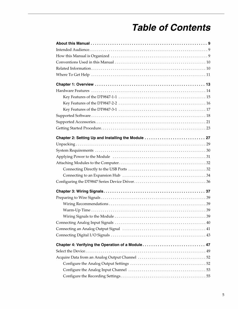
Table of Contents
Table of Contents
About this Manual . . . . . . . . . . . . . . . . . . . . . . . . . . . . . . . . . . . . . . . . . . . . . . . . . . . . . . 9
Intended Audience. . . . . . . . . . . . . . . . . . . . . . . . . . . . . . . . . . . . . . . . . . . . . . . . . . . . . . . . . . . . . 9
How this Manual is Organized . . . . . . . . . . . . . . . . . . . . . . . . . . . . . . . . . . . . . . . . . . . . . . . . . . 9
Conventions Used in this Manual . . . . . . . . . . . . . . . . . . . . . . . . . . . . . . . . . . . . . . . . . . . . . . . 10
Related Information . . . . . . . . . . . . . . . . . . . . . . . . . . . . . . . . . . . . . . . . . . . . . . . . . . . . . . . . . . . 10
Where To Get Help . . . . . . . . . . . . . . . . . . . . . . . . . . . . . . . . . . . . . . . . . . . . . . . . . . . . . . . . . . . 11
Chapter 1: Overview . . . . . . . . . . . . . . . . . . . . . . . . . . . . . . . . . . . . . . . . . . . . . . . . . . . 13
Hardware Features . . . . . . . . . . . . . . . . . . . . . . . . . . . . . . . . . . . . . . . . . . . . . . . . . . . . . . . . . . . 14
Key Features of the DT9847-1-1 . . . . . . . . . . . . . . . . . . . . . . . . . . . . . . . . . . . . . . . . . . . . . 15
Key Features of the DT9847-2-2 . . . . . . . . . . . . . . . . . . . . . . . . . . . . . . . . . . . . . . . . . . . . . 16
Key Features of the DT9847-3-1 . . . . . . . . . . . . . . . . . . . . . . . . . . . . . . . . . . . . . . . . . . . . . 17
Supported Software . . . . . . . . . . . . . . . . . . . . . . . . . . . . . . . . . . . . . . . . . . . . . . . . . . . . . . . . . . . 18
Supported Accessories. . . . . . . . . . . . . . . . . . . . . . . . . . . . . . . . . . . . . . . . . . . . . . . . . . . . . . . . . 21
Getting Started Procedure. . . . . . . . . . . . . . . . . . . . . . . . . . . . . . . . . . . . . . . . . . . . . . . . . . . . . . 23
Chapter 2: Setting Up and Installing the Module . . . . . . . . . . . . . . . . . . . . . . . . . . . . 27
Unpacking . . . . . . . . . . . . . . . . . . . . . . . . . . . . . . . . . . . . . . . . . . . . . . . . . . . . . . . . . . . . . . . . . . . 29
System Requirements . . . . . . . . . . . . . . . . . . . . . . . . . . . . . . . . . . . . . . . . . . . . . . . . . . . . . . . . . 30
Applying Power to the Module . . . . . . . . . . . . . . . . . . . . . . . . . . . . . . . . . . . . . . . . . . . . . . . . 31
Attaching Modules to the Computer. . . . . . . . . . . . . . . . . . . . . . . . . . . . . . . . . . . . . . . . . . . . . 32
Connecting Directly to the USB Ports . . . . . . . . . . . . . . . . . . . . . . . . . . . . . . . . . . . . . . . . 32
Connecting to an Expansion Hub . . . . . . . . . . . . . . . . . . . . . . . . . . . . . . . . . . . . . . . . . . . 34
Configuring the DT9847 Series Device Driver . . . . . . . . . . . . . . . . . . . . . . . . . . . . . . . . . . . . . 36
Chapter 3: Wiring Signals . . . . . . . . . . . . . . . . . . . . . . . . . . . . . . . . . . . . . . . . . . . . . . . 37
Preparing to Wire Signals . . . . . . . . . . . . . . . . . . . . . . . . . . . . . . . . . . . . . . . . . . . . . . . . . . . . . . 39
Wiring Recommendations . . . . . . . . . . . . . . . . . . . . . . . . . . . . . . . . . . . . . . . . . . . . . . . . . . 39
Warm-Up Time . . . . . . . . . . . . . . . . . . . . . . . . . . . . . . . . . . . . . . . . . . . . . . . . . . . . . . . . . . . 39
Wiring Signals to the Module . . . . . . . . . . . . . . . . . . . . . . . . . . . . . . . . . . . . . . . . . . . . . . . 39
Connecting Analog Input Signals . . . . . . . . . . . . . . . . . . . . . . . . . . . . . . . . . . . . . . . . . . . . . . . 40
Connecting an Analog Output Signal . . . . . . . . . . . . . . . . . . . . . . . . . . . . . . . . . . . . . . . . . . . 41
Connecting Digital I/O Signals . . . . . . . . . . . . . . . . . . . . . . . . . . . . . . . . . . . . . . . . . . . . . . . . . 43
Chapter 4: Verifying the Operation of a Module . . . . . . . . . . . . . . . . . . . . . . . . . . . . . 47
Select the Device . . . . . . . . . . . . . . . . . . . . . . . . . . . . . . . . . . . . . . . . . . . . . . . . . . . . . . . . . . . . . . 49
Acquire Data from an Analog Output Channel . . . . . . . . . . . . . . . . . . . . . . . . . . . . . . . . . . . 52
Configure the Analog Output Settings . . . . . . . . . . . . . . . . . . . . . . . . . . . . . . . . . . . . . . . 52
Configure the Analog Input Channel . . . . . . . . . . . . . . . . . . . . . . . . . . . . . . . . . . . . . . . . 53
Configure the Recording Settings. . . . . . . . . . . . . . . . . . . . . . . . . . . . . . . . . . . . . . . . . . . . 55
5

Contents
6
Configure the Acquisition Settings. . . . . . . . . . . . . . . . . . . . . . . . . . . . . . . . . . . . . . . . . . . 56
Start the Operation . . . . . . . . . . . . . . . . . . . . . . . . . . . . . . . . . . . . . . . . . . . . . . . . . . . . . . . . 57
Chapter 5: Principles of Operation . . . . . . . . . . . . . . . . . . . . . . . . . . . . . . . . . . . . . . . 61
Analog Input Features . . . . . . . . . . . . . . . . . . . . . . . . . . . . . . . . . . . . . . . . . . . . . . . . . . . . . . . . . 64
Analog Input Channels . . . . . . . . . . . . . . . . . . . . . . . . . . . . . . . . . . . . . . . . . . . . . . . . . . . . 64
Input Ranges and Gains . . . . . . . . . . . . . . . . . . . . . . . . . . . . . . . . . . . . . . . . . . . . . . . . . . . . 64
IEPE Functions. . . . . . . . . . . . . . . . . . . . . . . . . . . . . . . . . . . . . . . . . . . . . . . . . . . . . . . . . . . . 65
Input Resolution . . . . . . . . . . . . . . . . . . . . . . . . . . . . . . . . . . . . . . . . . . . . . . . . . . . . . . . . . . 65
Input Clock Source . . . . . . . . . . . . . . . . . . . . . . . . . . . . . . . . . . . . . . . . . . . . . . . . . . . . . . . . 65
Configuration Delay . . . . . . . . . . . . . . . . . . . . . . . . . . . . . . . . . . . . . . . . . . . . . . . . . . . 66
Analog Input Conversion Modes . . . . . . . . . . . . . . . . . . . . . . . . . . . . . . . . . . . . . . . . . . . . 66
Single-Value Operations . . . . . . . . . . . . . . . . . . . . . . . . . . . . . . . . . . . . . . . . . . . . . . . 66
Single-Values Operations . . . . . . . . . . . . . . . . . . . . . . . . . . . . . . . . . . . . . . . . . . . . . . 67
Continuous Scan Mode . . . . . . . . . . . . . . . . . . . . . . . . . . . . . . . . . . . . . . . . . . . . . . . . 67
Input Triggers . . . . . . . . . . . . . . . . . . . . . . . . . . . . . . . . . . . . . . . . . . . . . . . . . . . . . . . . . . . . 69
Start Trigger Sources . . . . . . . . . . . . . . . . . . . . . . . . . . . . . . . . . . . . . . . . . . . . . . . . . . 69
Reference Trigger Sources . . . . . . . . . . . . . . . . . . . . . . . . . . . . . . . . . . . . . . . . . . . . . . 70
Data Format and Transfer . . . . . . . . . . . . . . . . . . . . . . . . . . . . . . . . . . . . . . . . . . . . . . . . . . 71
Error Conditions . . . . . . . . . . . . . . . . . . . . . . . . . . . . . . . . . . . . . . . . . . . . . . . . . . . . . . . . . . 71
Analog Output Features . . . . . . . . . . . . . . . . . . . . . . . . . . . . . . . . . . . . . . . . . . . . . . . . . . . . . . . 72
Analog Output Channels . . . . . . . . . . . . . . . . . . . . . . . . . . . . . . . . . . . . . . . . . . . . . . . . . . . 72
Output Ranges and Gains . . . . . . . . . . . . . . . . . . . . . . . . . . . . . . . . . . . . . . . . . . . . . . . . . . 72
Output Resolution. . . . . . . . . . . . . . . . . . . . . . . . . . . . . . . . . . . . . . . . . . . . . . . . . . . . . . . . . 72
Output Clocks . . . . . . . . . . . . . . . . . . . . . . . . . . . . . . . . . . . . . . . . . . . . . . . . . . . . . . . . . . . . 72
Output Conversion Modes . . . . . . . . . . . . . . . . . . . . . . . . . . . . . . . . . . . . . . . . . . . . . . . . . 73
Single-Value Mode . . . . . . . . . . . . . . . . . . . . . . . . . . . . . . . . . . . . . . . . . . . . . . . . . . . . 73
Waveform Generation Mode . . . . . . . . . . . . . . . . . . . . . . . . . . . . . . . . . . . . . . . . . . . . 73
Continuous Analog Output Operations . . . . . . . . . . . . . . . . . . . . . . . . . . . . . . . . . . 74
Output Trigger. . . . . . . . . . . . . . . . . . . . . . . . . . . . . . . . . . . . . . . . . . . . . . . . . . . . . . . . . . . . 75
Data Format and Transfer . . . . . . . . . . . . . . . . . . . . . . . . . . . . . . . . . . . . . . . . . . . . . . . . . . 76
Error Conditions . . . . . . . . . . . . . . . . . . . . . . . . . . . . . . . . . . . . . . . . . . . . . . . . . . . . . . . . . . 76
Digital I/O Features. . . . . . . . . . . . . . . . . . . . . . . . . . . . . . . . . . . . . . . . . . . . . . . . . . . . . . . . . . . 77
Digital I/O Lines . . . . . . . . . . . . . . . . . . . . . . . . . . . . . . . . . . . . . . . . . . . . . . . . . . . . . . . . . . 77
Operation Modes. . . . . . . . . . . . . . . . . . . . . . . . . . . . . . . . . . . . . . . . . . . . . . . . . . . . . . . . . . 77
Triggering Acquisition on Multiple Modules . . . . . . . . . . . . . . . . . . . . . . . . . . . . . . . . . . . . . 78
Synchronizing Acquisition on Multiple DT9847 Series Modules . . . . . . . . . . . . . . . . . . . . . 79
Triggering DT9847 and DT9837 Series Modules Using the Sync Bus. . . . . . . . . . . . . . 81

Contents
Chapter 6: Supported Device Driver Capabilities. . . . . . . . . . . . . . . . . . . . . . . . . . . . 85
Data Flow and Operation Options. . . . . . . . . . . . . . . . . . . . . . . . . . . . . . . . . . . . . . . . . . . . . . . 87
Buffering . . . . . . . . . . . . . . . . . . . . . . . . . . . . . . . . . . . . . . . . . . . . . . . . . . . . . . . . . . . . . . . . . . . . 88
Triggered Scan Mode. . . . . . . . . . . . . . . . . . . . . . . . . . . . . . . . . . . . . . . . . . . . . . . . . . . . . . . . . . 88
Data Encoding. . . . . . . . . . . . . . . . . . . . . . . . . . . . . . . . . . . . . . . . . . . . . . . . . . . . . . . . . . . . . . . . 88
Channels . . . . . . . . . . . . . . . . . . . . . . . . . . . . . . . . . . . . . . . . . . . . . . . . . . . . . . . . . . . . . . . . . . . . 89
Gain . . . . . . . . . . . . . . . . . . . . . . . . . . . . . . . . . . . . . . . . . . . . . . . . . . . . . . . . . . . . . . . . . . . . . . . . 89
Ranges . . . . . . . . . . . . . . . . . . . . . . . . . . . . . . . . . . . . . . . . . . . . . . . . . . . . . . . . . . . . . . . . . . . . . . 90
Resolution . . . . . . . . . . . . . . . . . . . . . . . . . . . . . . . . . . . . . . . . . . . . . . . . . . . . . . . . . . . . . . . . . . . 90
Current and Resistance Support . . . . . . . . . . . . . . . . . . . . . . . . . . . . . . . . . . . . . . . . . . . . . . . . 90
Thermocouple, RTD, and Thermistor Support . . . . . . . . . . . . . . . . . . . . . . . . . . . . . . . . . . . . 91
IEPE Support. . . . . . . . . . . . . . . . . . . . . . . . . . . . . . . . . . . . . . . . . . . . . . . . . . . . . . . . . . . . . . . . . 92
Bridge and Strain Gage Support . . . . . . . . . . . . . . . . . . . . . . . . . . . . . . . . . . . . . . . . . . . . . . . . 92
Start Triggers. . . . . . . . . . . . . . . . . . . . . . . . . . . . . . . . . . . . . . . . . . . . . . . . . . . . . . . . . . . . . . . . . 93
Reference Triggers . . . . . . . . . . . . . . . . . . . . . . . . . . . . . . . . . . . . . . . . . . . . . . . . . . . . . . . . . . . . 94
Clocks . . . . . . . . . . . . . . . . . . . . . . . . . . . . . . . . . . . . . . . . . . . . . . . . . . . . . . . . . . . . . . . . . . . . . . . 95
Counter/Timers . . . . . . . . . . . . . . . . . . . . . . . . . . . . . . . . . . . . . . . . . . . . . . . . . . . . . . . . . . . . . . 96
Tachometers . . . . . . . . . . . . . . . . . . . . . . . . . . . . . . . . . . . . . . . . . . . . . . . . . . . . . . . . . . . . . . . . . 97
Chapter 7: Troubleshooting . . . . . . . . . . . . . . . . . . . . . . . . . . . . . . . . . . . . . . . . . . . . . 99
General Checklist . . . . . . . . . . . . . . . . . . . . . . . . . . . . . . . . . . . . . . . . . . . . . . . . . . . . . . . . . . . . 100
Technical Support . . . . . . . . . . . . . . . . . . . . . . . . . . . . . . . . . . . . . . . . . . . . . . . . . . . . . . . . . . . 102
If Your Module Needs Factory Service . . . . . . . . . . . . . . . . . . . . . . . . . . . . . . . . . . . . . . . . . 103
Chapter 8: Calibration . . . . . . . . . . . . . . . . . . . . . . . . . . . . . . . . . . . . . . . . . . . . . . . . . 105
Using the Calibration Utility . . . . . . . . . . . . . . . . . . . . . . . . . . . . . . . . . . . . . . . . . . . . . . . . . . 107
Calibrating the Analog Input Subsystem . . . . . . . . . . . . . . . . . . . . . . . . . . . . . . . . . . . . . . . 108
Warming up the Module . . . . . . . . . . . . . . . . . . . . . . . . . . . . . . . . . . . . . . . . . . . . . . . . . . 108
Connecting a Precision Voltage Source . . . . . . . . . . . . . . . . . . . . . . . . . . . . . . . . . . . . . . 108
Using the Auto-Calibration Procedure . . . . . . . . . . . . . . . . . . . . . . . . . . . . . . . . . . . . . . 108
Using the Manual Calibration Procedure . . . . . . . . . . . . . . . . . . . . . . . . . . . . . . . . . . . . 109
Calibrating the Analog Output Subsystem . . . . . . . . . . . . . . . . . . . . . . . . . . . . . . . . . . . . . . 110
Appendix A: Specifications . . . . . . . . . . . . . . . . . . . . . . . . . . . . . . . . . . . . . . . . . . . . 111
Analog Input Specifications . . . . . . . . . . . . . . . . . . . . . . . . . . . . . . . . . . . . . . . . . . . . . . . . . . . 112
Analog Output Specifications. . . . . . . . . . . . . . . . . . . . . . . . . . . . . . . . . . . . . . . . . . . . . . . . . . 117
Digital I/O Specifications . . . . . . . . . . . . . . . . . . . . . . . . . . . . . . . . . . . . . . . . . . . . . . . . . . . . . 119
Trigger Specifications . . . . . . . . . . . . . . . . . . . . . . . . . . . . . . . . . . . . . . . . . . . . . . . . . . . . . . . . 120
Master Oscillator Specifications . . . . . . . . . . . . . . . . . . . . . . . . . . . . . . . . . . . . . . . . . . . . . . . . 121
Power, Physical, and Environmental Specifications . . . . . . . . . . . . . . . . . . . . . . . . . . . . . . . 122
Regulatory Specifications . . . . . . . . . . . . . . . . . . . . . . . . . . . . . . . . . . . . . . . . . . . . . . . . . . . . . 123
Connector Specifications . . . . . . . . . . . . . . . . . . . . . . . . . . . . . . . . . . . . . . . . . . . . . . . . . . . . . . 124
External Power Supply Specifications. . . . . . . . . . . . . . . . . . . . . . . . . . . . . . . . . . . . . . . . . . . 125
7

Contents
8
Appendix B: Connector Pin Assignments and LED Status Indicators . . . . . . . . . 127
Digital I/O and External Trigger Connector . . . . . . . . . . . . . . . . . . . . . . . . . . . . . . . . . . . . . 128
External USB Connector . . . . . . . . . . . . . . . . . . . . . . . . . . . . . . . . . . . . . . . . . . . . . . . . . . . . . . 129
External Power Connector . . . . . . . . . . . . . . . . . . . . . . . . . . . . . . . . . . . . . . . . . . . . . . . . . . . . 130
STP15 Screw Terminal Panel . . . . . . . . . . . . . . . . . . . . . . . . . . . . . . . . . . . . . . . . . . . . . . . . . . 131
LED Status Indicators . . . . . . . . . . . . . . . . . . . . . . . . . . . . . . . . . . . . . . . . . . . . . . . . . . . . . . . . 132
Appendix C: Powering OEM Modules . . . . . . . . . . . . . . . . . . . . . . . . . . . . . . . . . . . . 133
Powering the DT9847-1-1-OEM Module . . . . . . . . . . . . . . . . . . . . . . . . . . . . . . . . . . . . . . . . 134
Powering the DT9847-2-2-OEM or DT9847-3-1-OEM Module . . . . . . . . . . . . . . . . . . . . . . 136
Appendix D: Register-Level Programming . . . . . . . . . . . . . . . . . . . . . . . . . . . . . . . 137
Writing to the EEPROM Register. . . . . . . . . . . . . . . . . . . . . . . . . . . . . . . . . . . . . . . . . . . . . . . 138
Index . . . . . . . . . . . . . . . . . . . . . . . . . . . . . . . . . . . . . . . . . . . . . . . . . . . . . . . . . . . . . . . 141

About this ManualThe first part of this manual describes how to install and set up your DT9847 Series module and device driver, and verify that your module is working properly.
The second part of this manual describes the features of the DT9847 Series modules, the capabilities of the DT9847 Series Device Driver, and how to program the DT9847 module using the DT-Open Layers for .NET Class Library software. Troubleshooting information is also provided.
Note: For more information on the class library, refer to the DT-Open Layers for .NET Class Library User’s Manual. If you are using the DataAcq SDK or a software application to program your device, refer to the documentation for that software for more information.
Intended Audience
This document is intended for engineers, scientists, technicians, or others responsible for using and/or programming a DT9847 Series module for data acquisition operations in the Microsoft® Windows Vista, Windows 7, Windows 8, or Windows 10 operating system. It is assumed that you have some familiarity with data acquisition principles and that you understand your application.
How this Manual is Organized
This manual is organized as follows:
• Chapter 1, “Overview,” describes the major features of the DT9847 Series module, as well as the supported software and accessories for the modules.
• Chapter 2, “Setting Up and Installing the Module,” describes how to install a DT9847 Series module, how to apply power to the module, and how to configure the DT9847 Series Device Driver.
• Chapter 3, “Wiring Signals,” describes how to wire signals to a DT9847 Series module.
• Chapter 4, “Verifying the Operation of a Module,” describes how to verify the operation of a DT9847 Series module with the QuickDAQ application.
• Chapter 5, “Principles of Operation,” describes all of the features of the DT9847 Series module and how to access them in your application.
• Chapter 6, “Supported Device Driver Capabilities,” lists the data acquisition subsystems and the associated features accessible using the DT9847 Series Device Driver.
• Chapter 7, “Troubleshooting,” provides information that you can use to resolve problems with the DT9847 Series module and DT9847 Series Device Driver, should they occur.
• Chapter 8, “Calibration,” describes how to calibrate the analog I/O circuitry of the DT9847 module.
9
About this Manual
10
• Appendix A, “Specifications,” lists the specifications of the DT9847 Series module.
• Appendix B, “Connector Pin Assignments and LED Status Indicators,” lists the pin assignments of the connectors on the DT9847 Series module, the screw terminal assignments of the STP15 screw terminal panel, and describes the LED status indicators on the DT9847 Series module.
• Appendix C, “Powering OEM Modules,” describes how to apply power to OEM modules.
• Appendix D, “Register-Level Programming,” describes how to write to the registers of the DT9847 Series modules to change the default settings that are defined in the Open Layers Control Panel programmatically.
• An index completes this manual.
Conventions Used in this Manual
The following conventions are used in this manual:
• Notes provide useful information or information that requires special emphasis, cautions provide information to help you avoid losing data or damaging your equipment, and warnings provide information to help you avoid catastrophic damage to yourself or your equipment.
• Items that you select or type are shown in bold.
Related Information
Refer to the following documents for more information on using the DT9847 Series module:
• QuickDAQ User’s Manual (UM-24774). This manual describes how to create a QuickDAQ application to acquire and analyze data from a DT-Open Layers data acquisition module.
• DT-Open Layers for .NET User’s Manual (UM-22161). For programmers who are developing their own application programs using Visual C# or Visual Basic .NET, this manual describes how to use the DT-Open Layers for .NET Class Library to access the capabilities of Data Translation data acquisition devices.
• DataAcq SDK User’s Manual (UM-18326). For programmers who are developing their own application programs using the Microsoft C compiler, this manual describes how to use the DT-Open Layers DataAcq SDK to access the capabilities of Data Translation data acquisition devices.
• LV-Link Online Help. This help file describes how to use LV-Link with the LabVIEW graphical programming language to access the capabilities of Data Translation data acquisition devices.
• Microsoft Windows 7, Windows 8, or Windows 10 documentation.
• USB web site (http://www.usb.org)

About this Manual
Where To Get Help
Should you run into problems installing or using a DT9847 Series module, the Technical Support Department is available to provide technical assistance. Refer to Chapter 7 for more information. If you are outside the United States or Canada, call your local distributor, whose number is listed on our web site www.mccdaq.com.
11

About this Manual
12

1Overview
Hardware Features. . . . . . . . . . . . . . . . . . . . . . . . . . . . . . . . . . . . . . . . . . . . . . . . . . . . . . . . . . . . 14
Supported Software . . . . . . . . . . . . . . . . . . . . . . . . . . . . . . . . . . . . . . . . . . . . . . . . . . . . . . . . . . . 18
Supported Accessories. . . . . . . . . . . . . . . . . . . . . . . . . . . . . . . . . . . . . . . . . . . . . . . . . . . . . . . . . 21
Getting Started Procedure. . . . . . . . . . . . . . . . . . . . . . . . . . . . . . . . . . . . . . . . . . . . . . . . . . . . . . 23
13

Chapter 1
14
Hardware Features DT9847 Series modules are high-accuracy, dynamic signal acquisition modules for the USB (Ver. 2.0 or Ver. 1.1) bus. These modules are ideal for acoustic measurements due to their AC coupling and frequency characteristics. Figure 1 shows the DT9847-3-1 module.
Figure 1: DT9847-3-1 Module
Table 1 lists the major differences between the modules.
Table 1: Major Differences Between the DT9847 Series Modules
Feature DT9847-1-1 DT9847-2-2 DT9847-3-1
Number of Analog Input Channels 1 2 3
Number of Analog Output Channels 1 2 1
Power USB Powera
a. Using USB-Y cable.
External Powerb
b. Using a 5 V to 24 V external power supply at 5 W.
External Powerb
Overview
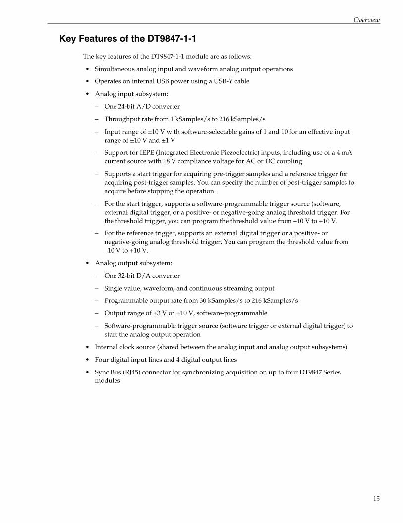
Key Features of the DT9847-1-1
The key features of the DT9847-1-1 module are as follows:
• Simultaneous analog input and waveform analog output operations
• Operates on internal USB power using a USB-Y cable
• Analog input subsystem:
One 24-bit A/D converter
Throughput rate from 1 kSamples/s to 216 kSamples/s
Input range of ±10 V with software-selectable gains of 1 and 10 for an effective input range of ±10 V and ±1 V
Support for IEPE (Integrated Electronic Piezoelectric) inputs, including use of a 4 mA current source with 18 V compliance voltage for AC or DC coupling
Supports a start trigger for acquiring pre-trigger samples and a reference trigger for acquiring post-trigger samples. You can specify the number of post-trigger samples to acquire before stopping the operation.
For the start trigger, supports a software-programmable trigger source (software, external digital trigger, or a positive- or negative-going analog threshold trigger. For the threshold trigger, you can program the threshold value from –10 V to +10 V.
For the reference trigger, supports an external digital trigger or a positive- or negative-going analog threshold trigger. You can program the threshold value from –10 V to +10 V.
• Analog output subsystem:
One 32-bit D/A converter
Single value, waveform, and continuous streaming output
Programmable output rate from 30 kSamples/s to 216 kSamples/s
Output range of ±3 V or ±10 V, software-programmable
Software-programmable trigger source (software trigger or external digital trigger) to start the analog output operation
• Internal clock source (shared between the analog input and analog output subsystems)
• Four digital input lines and 4 digital output lines
• Sync Bus (RJ45) connector for synchronizing acquisition on up to four DT9847 Series modules
15

Chapter 1
16
Key Features of the DT9847-2-2
The key hardware features of the DT9847-2-2 module are as follows:
• Simultaneous analog input and analog output operations (continuous or waveform mode)
• Operates on external USB power
• Analog input subsystem:
Two, simultaneous 24-bit A/D converters
Throughput rate from 1 kSamples/s to 216 kSamples/s for simultaneous, high-resolution measurements
Input range of ±10 V with software-selectable gains of 1 and 10 for an effective input range of ±10 V and ±1 V
Support for IEPE (Integrated Electronic Piezoelectric) inputs, including use of a 4 mA current source with 18 V compliance voltage for AC or DC coupling
Supports a start trigger for acquiring pre-trigger samples and a reference trigger for acquiring post-trigger samples. You can specify the number of post-trigger samples to acquire before stopping the operation.
For the start trigger, supports a software-programmable trigger source (software, external digital trigger, or a positive- or negative-going analog threshold trigger on any of the analog input channels). For the threshold trigger, you can program the threshold value from –10 V to +10 V.
For the reference trigger, supports an external digital trigger or a positive- or negative-going analog threshold trigger on any of the analog input channels. You can program the threshold value from –10 V to +10 V.
• Analog output subsystem:
Two 32-bit D/A converters
Single value, waveform, and continuous streaming output
Programmable output rate from 30 kSamples/s to 216 kSamples/s
Output range of ±3 V or ±10 V, software programmable
Software-programmable trigger source (software trigger or external digital trigger) to start the analog output operation
• Internal clock source (shared between the analog input and analog output subsystems)
• Sync Bus (RJ45) connector for synchronizing acquisition on up to four DT9847 Series modules
• Requires use of an external +5 VDC to +24 VDC power supply
Overview
Key Features of the DT9847-3-1
The key hardware features of the DT9847-3-1 module are as follows:
• Simultaneous analog input and analog output operations (continuous or waveform mode)
• Operates on external USB power
• Analog input subsystem:
Three, simultaneous 24-bit A/D converters
Throughput rate from 1 kSamples/s to 216 kSamples/s for simultaneous, high-resolution measurements
Input range of ±10 V with software-selectable gains of 1 and 10 for an effective input range of ±10 V and ±1 V
Support for IEPE (Integrated Electronic Piezoelectric) inputs, including use of a 4 mA current source with 18 V compliance voltage for AC or DC coupling
Supports a start trigger for acquiring pre-trigger samples and a reference trigger for acquiring post-trigger samples. You can specify the number of post-trigger samples to acquire before stopping the operation.
For the start trigger, supports a software-programmable trigger source (software, external digital trigger, or a positive- or negative-going analog threshold trigger on any of the analog input channels). For the threshold trigger, you can program the threshold value from –10 V to +10 V.
For the reference trigger, supports an external digital trigger or a positive- or negative-going analog threshold trigger on any of the analog input channels. You can program the threshold value from –10 V to +10 V.
• Analog output subsystem:
One 32-bit D/A converter
Single value, waveform, and continuous streaming output
Programmable output rate from 30 kSamples/s to 216 kSamples/s
Output range of ±3 V or ±10 V, software programmable
Software-programmable trigger source (software trigger or external digital trigger) to start the analog output operation
• Internal clock source (shared between the analog input and analog output subsystems)
• Sync Bus (RJ45) connector for synchronizing acquisition on up to four DT9847 Series modules
• Requires use of an external +5 VDC to +24 VDC power supply
17
Chapter 1
18
Supported SoftwareThe DT Omni installer includes the following software for use with the DT9847 Series modules:
• DT9847 Series Device Driver – The DT9847 Series Device Driver allows you to use a DT9847 Series module with any of the supported software packages or utilities.
• DT9847 Series Calibration Utility – This utility, described in Chapter 8 starting on page 105, allows you to calibrate the analog input and analog output circuitry of a DT9847 Series module.
• QuickDAQ Base Version – The base version of QuickDAQ is free-of-charge and allows you to acquire and analyze data from all Data Translation USB and Ethernet devices, except the DT9841 Series, DT9817, DT9835, and DT9853/54. Using the base version of QuickDAQ, you can perform the following functions:
Discover and select your devices.
Configure all input channel settings for the attached sensors.
Load/save multiple hardware configurations.
Generate output stimuli (fixed waveforms, swept sine waves, or noise signals).
On each supported data acquisition device, acquire data from all channels supported in the input channel list.
Choose to acquire data continuously or for a specified duration.
Choose software or triggered acquisition.
Log acquired data to disk in an .hpf file.
Display acquired data during acquisition in either a digital display using the Channel Display window or as a waveform in the Channel Plot window.
Choose linear or logarithmic scaling for the horizontal and vertical axes.
View statistics about the acquired data, including the minimum, maximum, and mean values and the standard deviation in the Statistics window.
Export time data to a .csv or .txt file; you can open the recorded data in Microsoft Excel® for further analysis.
Read a previously recorded .hpf data file.
Customize many aspects of the acquisition, display, and recording functions to suit your needs, including the acquisition duration, sampling frequency, trigger settings, filter type, and temperature units to use.

Overview
• QuickDAQ FFT Analysis Option – When enabled with a purchased license key, the QuickDAQ FFT Analysis option includes all the features of the QuickDAQ Base version plus basic FFT analysis features, including the following:
The ability to switch between the Data Logger time-based interface and the FFT Analyzer block/average-based interface.
Supports software, freerun, or triggered acquisition with accept and reject controls for impact testing applications.
Allows you to perform single-channel FFT (Fast Fourier Transform) operations, including AutoSpectrum, Spectrum, and Power Spectral Density, on the acquired analog input data. You can configure a number of parameters for the FFT, including the FFT size, windowing type, averaging type, integration type, and so on.
Allows you to display frequency-domain data as amplitude or phase.
Supports dB or linear scaling with RMS (root mean squared), peak, and peak-to-peak scaling options
Supports linear or exponential averaging with RMS, vector, and peak hold averaging options.
Supports windowed time channels.
Supports the following response window types: Hanning, Hamming, Bartlett, Blackman, Blackman Harris, and Flat top.
Supports the ability to lock the waveform output to the analysis frame time.
Allows you to configure and view dynamic performance statistics, including the input below full-scale (IBF), total harmonic distortion (THD), spurious free dynamic range (SFDR), signal-to-noise and distortion ratio (SINAD), signal-to-noise ratio (SNR), and the effective number of bits (ENOB), for selected time-domain channels in the Statistics window.
Supports digital IIR (infinite impulse response) filters.
• QuickDAQ Advanced FFT Analysis Option – When enabled with a purchased software license, the QuickDAQ Advanced FFT Analysis option includes all the features of the QuickDAQ Base version with the FFT Analysis option plus advanced FFT analysis features, including the following:
Allows you to designate a channel as a Reference or Response channel.
Allows you to perform two-channel FFT analysis functions, including Frequency Response Functions (Inertance, Mobility, Compliance, Apparent Mass, Impedance, Dynamic Stiffness, or custom FRF) with H1, H2, or H3 estimator types, Cross-Spectrum, Cross Power Spectral Density, Coherence, and Coherent Output Power.
Supports the Exponential response window type.
Supports the following reference window types: Hanning, Hamming, Bartlett, Blackman, Blackman Harris, FlatTop, Exponential, Force, and Cosine Taper windows.
Supports real, imaginary, and Nyquist display functions.
Allows you to save data in the .uff file format.
19

Chapter 1
20
• Quick DataAcq application –The Quick DataAcq application provides a quick way to get up and running using a DT9847 Series module. Using this application, you can verify key features of the modules, display data on the screen, and save data to disk. (Note that this application does not support configuring AC/DC coupling or the excitation current source for IEPE inputs.)
• DT-Open Layers for .NET Class Library – Use this class library if you want to use Visual C# or Visual Basic for .NET to develop your own application software for a DT9847 Series module using Visual Studio 2003-2012; the class library complies with the DT-Open Layers standard.
• DataAcq SDK – Use the Data Acq SDK if you want to use Visual Studio 6.0 and Microsoft C or C++ to develop your own application software for a DT9847 Series module using Windows Vista, Windows 7, or Windows 8; the DataAcq SDK complies with the DT-Open Layers standard.
• DAQ Adaptor for MATLAB – A link to the DAQ Adaptor for MATLAB is included from the DT Omni installer. Data Translation’s DAQ Adaptor provides an interface between the MATLAB Data Acquisition (DAQ) subsystem from The MathWorks and Data Translation’s DT-Open Layers architecture.
• LV-Link – A link to LV-Link is included from the DT Omni installer. Use LV-Link if you want to use the LabVIEW graphical programming language to access the capabilities of the DT9847 Series module.
Refer to the web site www.mccdaq.com for information about selecting the right software package for your needs.

Overview
Supported AccessoriesThe following optional accessories are available for the DT9847 Series:
• STP15 screw terminal panel – A screw terminal panel that accepts digital input signals and an external trigger input signal and provides connections for digital output signals.
The 15-pin, 2-meter, EP337 cable is included with the STP15 screw terminal panel. The EP337 cable allows you to attach the STP15 screw terminal panel to the Digital I/O and External Trigger connector on a DT9847 Series module.
Figure 3 shows the STP15 and EP337 cable.
Figure 2: STP15 Screw Terminal Panel and EP337 Cable
21

Chapter 1
22
• EP386 panel – The EP388 panel, shown in Figure 3, contains four RJ45 connectors that are wired in parallel, making it useful when attaching up to four DT9847 Series modules together using the Sync Bus connector. Refer to page 79 for more information on using this panel.
Figure 3: EP386 Panel
• BNC DIN Rail Kit – The BNC DIN Rail Kit, shown in Figure 4, allows you to mount USB modules that are packaged in metal boxes in a DIN rail. The kit includes mounting clips, screws, and instructions. The rail is not included.
Figure 4: BNC DIN Rail Kit

Overview
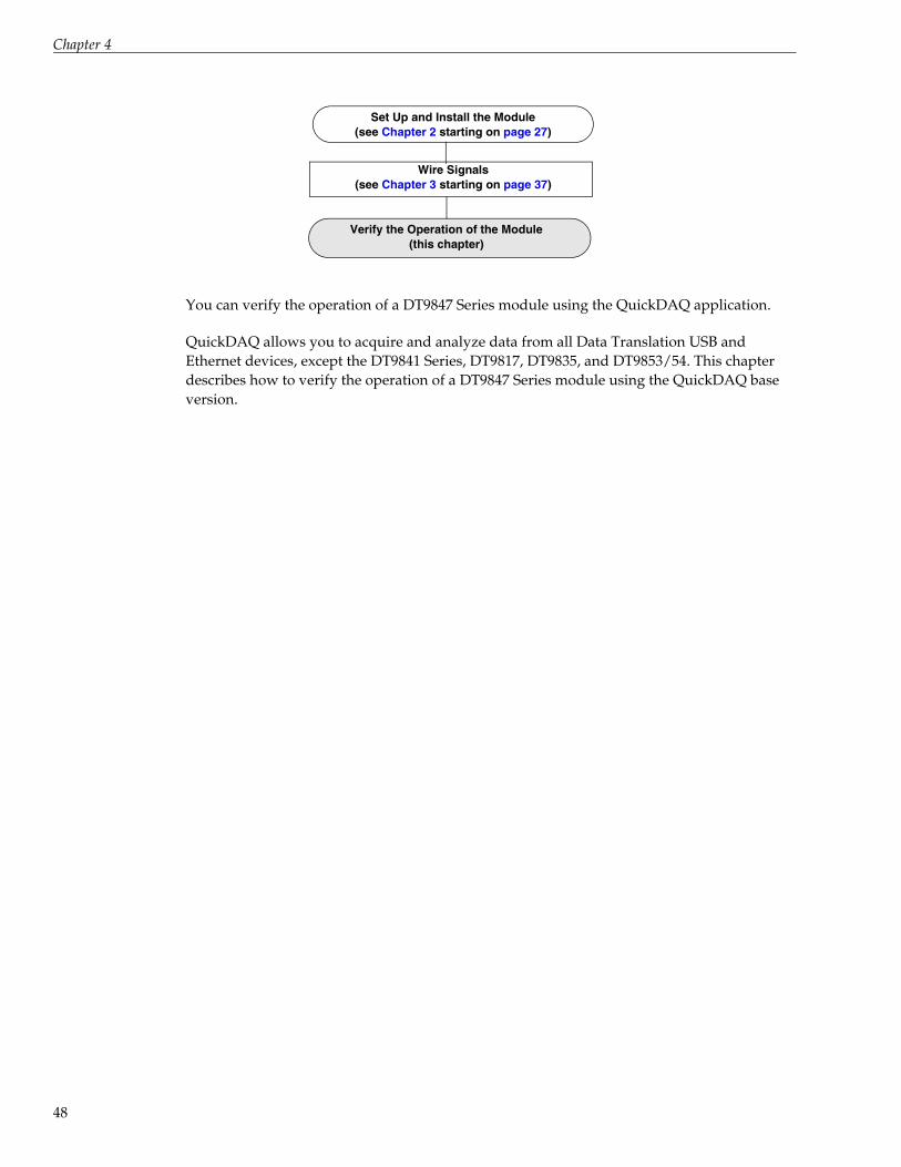
Getting Started ProcedureThe flow diagram shown in Figure 5 illustrates the steps needed to get started using a DT9847 Series module. This diagram is repeated in each Getting Started chapter; the shaded area in the diagram shows you where you are in the getting started procedure.
Figure 5: Getting Started Flow Diagram
Set Up and Install the Module(see Chapter 2 starting on page 27)
Wire Signals(see Chapter 3 starting on page 37)
Verify the Operation of the Module(see Chapter 4 starting on page 47)
23

Chapter 1
24

Part 1: Getting Started


2Setting Up and Installing the Module
Unpacking . . . . . . . . . . . . . . . . . . . . . . . . . . . . . . . . . . . . . . . . . . . . . . . . . . . . . . . . . . . . . . . . . . . 29
System Requirements . . . . . . . . . . . . . . . . . . . . . . . . . . . . . . . . . . . . . . . . . . . . . . . . . . . . . . . . . 30
Applying Power to the Module . . . . . . . . . . . . . . . . . . . . . . . . . . . . . . . . . . . . . . . . . . . . . . . . . 31
Attaching Modules to the Computer. . . . . . . . . . . . . . . . . . . . . . . . . . . . . . . . . . . . . . . . . . . . . 32
Configuring the DT9847 Series Device Driver . . . . . . . . . . . . . . . . . . . . . . . . . . . . . . . . . . . . . 36
27

Chapter 2
28
Set Up and Install the Module(this chapter)
Wire Signals(see Chapter 3 starting on page 37)
Verify the Operation of the Module(see Chapter 4 starting on page 47)

Setting Up and Installing the Module
UnpackingOpen the shipping box and verify that the following items are present:
• DT9847-1-1, DT9847-1-1-OEM, DT9847-2-2, DT9847-2-2-OEM, DT9847-3-1, or DT9847-3-1-OEM module
• If you ordered a DT9847-1-1 or DT98471-1-OEM module, the EP399 USB-Y cable is included. Optionally, you can use a +5 V external power supply (not included) to power the DT9847-1-1-OEM module.
• If you ordered a DT9847-2-2 or DT9847-3-1 module, the EP365 USB cable and EP394 +5 V external power supply are included.
• If you ordered a DT9847-2-2-OEM or DT9847-3-1-OEM module, the EP365 USB cable is included. To power the module, you must use a 5 V to 24 V external power supply (not included).
If an item is missing or damaged, contact Data Translation. If you are in the United States, call the Customer Service Department at (508) 956-5100. An application engineer will guide you through the appropriate steps for replacing missing or damaged items. If you are located outside the United States, call your local distributor (see www.mccdaq.com for more information).
Note: The DT9847 Series modules are factory-calibrated. If you decide that you want to recalibrate the analog input or analog output circuitry, refer to the instructions in Chapter 8.
CAUTION:
Ensure that the maximum voltage of the external supply is +5 V ±0.30 V. @ 600 mA. Higher voltages will destroy the DT9847-1-1-OEM module.
29

Chapter 2
30
System RequirementsFor reliable operation, ensure that your computer meets the following system requirements:
• Processor: Pentium 4/M or equivalent
• RAM: 1 GB
• Screen Resolution: 1024 x 768 pixels
• Operating System: Windows 10, Windows 8, Windows 7, Windows Vista (32- and 64-bit)
• Disk Space: 4 GB

Setting Up and Installing the Module
Applying Power to the Module The DT9847-1-1 module runs on USB power and does not use an external power supply. The DT9847-2-2 and DT9847-3-1 modules require an external power supply and are shipped with an EP394 +5V power supply and cable.
Note: If you are using the OEM version of a DT9847 Series module, refer to Appendix C starting on page 133 for information on powering the module.
To apply power to the module, do the following:
1. Connect the EP394 +5 V power supply to the external power connector on the DT9847 Series module. Refer to Figure 6.
Figure 6: Attaching a +5 V Power Supply to the DT9847 Series Module
2. Plug the power supply into a wall outlet.
To wall outlet
EP394 +5 V Power
DT9847 Series Module
Ext. Power Connector
31
Chapter 2
32
Attaching Modules to the ComputerThis section describes how to attach a DT9847 Series module to the host computer.
Note: Most computers have several USB ports that allow direct connection to USB devices. If your application requires more DT9847 Series modules than you have USB ports for, you can expand the number of USB devices attached to a single USB port by using expansion hubs. For more information, refer to page 34.
You can unplug a module, then plug it in again, if you wish, without causing damage. This process is called hot-swapping. Your application may take a few seconds to recognize a module once it is plugged back in.
The DT9847 Series modules use less than 500 mA; therefore, they do not require an external power supply.
You must install the device driver for your module before connecting the module(s) to the host computer. Run the DT Omni software to install the device driver and other software for the module.
Connecting Directly to the USB Ports
To connect a DT9847 Series module directly to a USB port on your computer, perform the following steps:
1. Attach one end of the USB cable to the USB port on the module and the other end to the USB port on your host computer.
If you are using the DT9847-1-1, use the EP399 USB-Y cable to connect the module to two USB ports on the host computer, as shown in Figure 7.

Setting Up and Installing the Module
Figure 7: Attaching the DT9847-1-1 Module to the Host Computer
Once the module is connected to the host computer, the operating system automatically detects the USB module and starts the Found New Hardware wizard.
2. For Windows Vista:
a. Click Locate and install driver software (recommended).The popup message "Windows needs your permission to continue" appears.
b. Click Continue.The Windows Security dialog box appears.
c. Click Install this driver software anyway.
Note: Windows 7, Windows 8, and Windows 10 find the device automatically.
3. Repeat these steps to attach another DT9847 Series module to the host computer, if desired.
DT9847-1-1 Module
USB Connector
Plug the USB B end of the USB-Y cable into the DT9847 Series module. Then, plug the two USB A ends of the cable into open USB ports on the computer.
This cable pulls power from both USB ports to power the module.
B end to module
A ends to host computer
EP399 USB-Y Cable
Trigger LED
USB LED
33

Chapter 2
34
Note: Once you have connected your module to the host computer, power is turned on to the module when your application program opens the module. The USB LED on the module turns green to indicate that power is turned on.
Power is turned off to the module when your application program terminates its connection to the module.
Connecting to an Expansion Hub
Expansion hubs are powered by their own external power supply. The practical number of DT9847 Series modules that you can connect to a single USB port depends on the throughput you want to achieve.
To connect multiple DT9847 Series modules to an expansion hub, do the following:
1. Attach one end of the USB cable to the module and the other end of the USB cable to an expansion hub.
If you are using the DT9847-1-1, use the EP399 USB-Y cable to connect the module to two USB ports on the expansion hub, as shown in Figure 8.
Figure 8: Attaching Multiple DT9847-1-1 Modules Using Expansion Hubs
2. Connect the power supply for the expansion hub to an external power supply.
3. Connect the expansion hub to the USB port on the host computer using another USB cable. Figure 9 shows how to attach DT9847-2-2 and DT9847-3-1 modules to an expansion hub.The operating system automatically detects the USB module and starts the Found New Hardware wizard.
USB Cable
Expansion Hubs
Host Computer
Power Supply for Hub
USB-Y Cable
USB-Y Cable
USB Cable
Power Supply for Hub
DT9847-1-1 Module
DT9847-1-1Module

Setting Up and Installing the Module
Figure 9: Attaching Multiple DT9847-2-2 and DT9847-3-1 Modules Using Expansion Hubs
4. For Windows Vista:
a. Click Locate and install driver software (recommended).The popup message "Windows needs your permission to continue" appears.
b. Click Continue.The Windows Security dialog box appears.
c. Click Install this driver software anyway.
Note: Windows 7, Windows 8, and Windows 10 find the device automatically.
5. Repeat these steps until you have attached the number of expansion hubs and modules that you require. The operating system automatically detects the USB devices as they are installed.
Note: Once you have connected your module to the host computer, power is turned on to the module when your application program opens a connection to the module. The LED on the module turns green to indicate that power is turned on.
Power is turned off to the module when your application program terminates its connection to the module.
USB Cable
Expansion Hubs
Host Computer
Power Supply for Hub
USB Cables
USB Cables
USB Cable
Power Supply for Hub
Power Supply for Module
*Note that each of these module requires a +5 V external power supply (EP394).
DT9847-2-2 or DT9847-3-1
Module
DT9847-2-2 or DT9847-3-1
ModuleDT9847-2-2 or
DT9847-3-1 Module
DT9847-2-2 or DT9847-3-1
Module
35

Chapter 2
36
Configuring the DT9847 Series Device Driver
Note: In Windows , you must have administrator privileges to run the Open Layers Control Panel. When you double-click the Open Layers Control Panel icon, you may see the Program Compatibility Assistant. If you do, select Open the control panel using recommended settings. You may also see a Windows message asking you if you want to run the Open Layers Control Panel as a "legacy CPL elevated." If you get this message, click Yes.
If you do not get this message and have trouble making changes in the Open Layers Control Panel, right click the DTOLCPL.CPL file and select Run as administrator. By default, this file is installed in the following location:
Windows (32-bit)C:\Windows\System32\Dtolcpl.cpl
Windows (64-bit)C:\Windows\SysWOW64\Dtolcpl.cpl
To configure the device driver for a DT9847 Series module, do the following:
1. If you have not already done so, power up the host computer and all peripherals.
2. From the Windows Start menu, select Settings|Control Panel.
3. From the Control Panel, double-click Open Layers Control Panel. The Data Acquisition Control Panel dialog box appears.
4. If you want to rename the module, click the name of the module that you want to rename, click Edit Name, enter a new name for the module, and then click OK. The name is used to identify the module in all subsequent applications.
5. Select the module that you want to configure, and then click Advanced.The Measurement Options dialog box appears.
6. For the Coupling type, select AC for AC coupling or DC for DC coupling for each analog input channel.
7. For the Current Source, select Enabled to enable the internal excitation current source or Disabled to disable the internal excitation current source for each analog input channel.
Note: If you enable the use of the internal excitation current source, it is recommended that you choose AC coupling. Refer to page 40 for more information on wiring IEPE inputs.
8. When you are finished, click OK to close the Measurement Options dialog box.
9. Repeat steps 4 to 8 for the other modules that you want to configure.
10. When you are finished configuring the modules, click Close to close the Control Panel.
3Wiring Signals
Preparing to Wire Signals . . . . . . . . . . . . . . . . . . . . . . . . . . . . . . . . . . . . . . . . . . . . . . . . . . . . . . 39
Connecting Analog Input Signals . . . . . . . . . . . . . . . . . . . . . . . . . . . . . . . . . . . . . . . . . . . . . . . 40
Connecting an Analog Output Signal . . . . . . . . . . . . . . . . . . . . . . . . . . . . . . . . . . . . . . . . . . . . 41
Connecting Digital I/O Signals . . . . . . . . . . . . . . . . . . . . . . . . . . . . . . . . . . . . . . . . . . . . . . . . . 43
37

Chapter 3
38
Set Up and Install the Module(see Chapter 2 starting on page 27)
Wire Signals(this chapter)
Verify the Operation of the Module(see Chapter 4 starting on page 47)
Wiring Signals
A
0DEC
A
AAt
Preparing to Wire SignalsThis section provides recommendations and information about wiring signals to a DT9847 Series module.
Wiring Recommendations
Keep the following recommendations in mind when wiring signals to a DT9847 Series module:
• Follow standard ESD procedures when wiring signals to the module.
• Separate power and signal lines by using physically different wiring paths or conduits.
• To avoid noise, do not locate the module and cabling next to sources that produce high electromagnetic fields, such as large electric motors, power lines, solenoids, and electric arcs, unless the signals are enclosed in a mumetal shield.
• Prevent electrostatic discharge to the I/O while the module is operational.
• Connect all unused analog input channels to analog ground.
Warm-Up Time
The DT9847 Series is ideal for acoustic measurements due to its AC coupling and frequency characteristics. It is not designed for DC stability; therefore, ensure that you allow the module to warm up for 15 minutes before use.
Wiring Signals to the Module
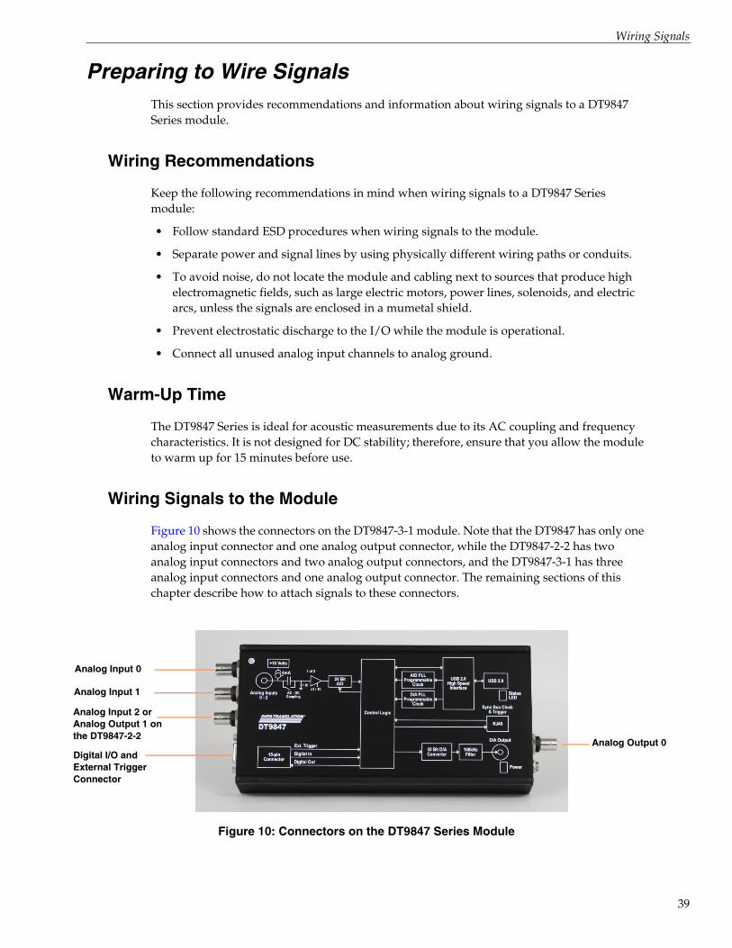
Figure 10 shows the connectors on the DT9847-3-1 module. Note that the DT9847 has only one analog input connector and one analog output connector, while the DT9847-2-2 has two analog input connectors and two analog output connectors, and the DT9847-3-1 has three analog input connectors and one analog output connector. The remaining sections of this chapter describe how to attach signals to these connectors.
Figure 10: Connectors on the DT9847 Series Module
nalog Input 0
Analog Outputigital I/O and xternal Trigger onnector
nalog Input 1
nalog Input 2 or nalog Output 1 on
he DT9847-2-2
39

Chapter 3
40
Connecting Analog Input SignalsFor the DT9847-1-1 module, you can connect one analog input signal (or IEPE sensor) to the BNC connector on the module. For the DT9847-2-2 module, you can connect up to two analog input signals (or IEPE sensors) to the BNC connectors on the module. For the DT9847-3-1 module, you can connect up to three analog input signals (or IEPE sensors) to the BNC connectors on the module. Internally, these signals are connected in single-ended mode. The DT9847 Series modules support an input signal range of ±10 V (using a gain of 1) or ±1 V (using a gain of 10).
Note: If you enable the use of the internal excitation current source for IEPE inputs, it is recommended that you choose AC coupling. Refer to page 64 for more information on IEPE inputs.
Figure 11 shows how to connect an analog input signal (channel 0, in this case) to a BNC connector on the DT9847 Series module.
Figure 11: Connecting Analog Inputs to a DT9847 Series Module
Signal Source
Analog Input 0

Wiring Signals
Connecting an Analog Output Signal The DT9847-1-1 and DT9847-3-1 modules provide one analog output channel. The DT9847-2-2 modules provides two analog input channels. The output channels have an output range of ±3 V.
Figure 12 shows how to connect an analog output signal to the DT9847-1-1 or DT9847-3-1 module.
Figure 12: Connecting an Analog Output Signal to the DT9847-1-1 or DT98473-1 Module
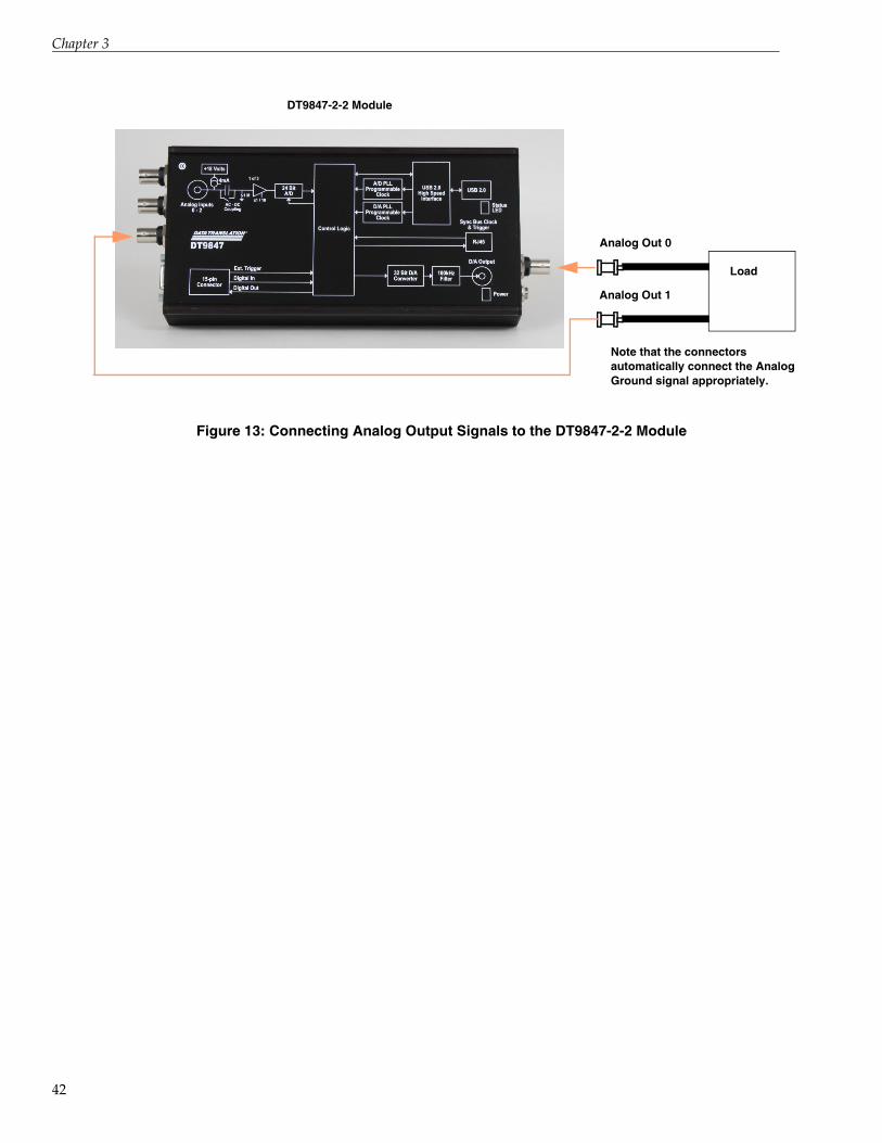
Figure 13 shows how to connect analog output signals to the DT9847-2-1 module.
Note that the connector automatically connects the Analog Ground signal
LoadAnalog Out 0
DT9847-1-1 or DT9847-3-1 Module
41
Chapter 3
42
Figure 13: Connecting Analog Output Signals to the DT9847-2-2 Module
Note that the connectors automatically connect the AnalogGround signal appropriately.
Load
Analog Out 0
DT9847-2-2 Module
Analog Out 1
Wiring Signals
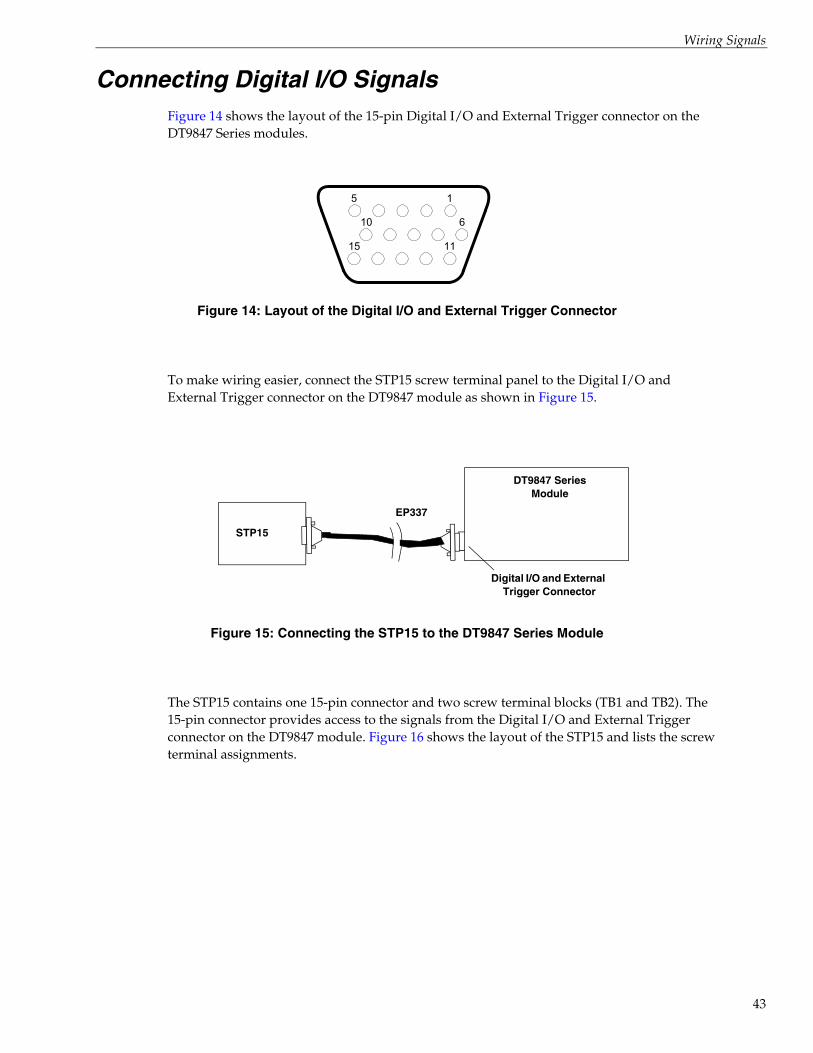
Connecting Digital I/O SignalsFigure 14 shows the layout of the 15-pin Digital I/O and External Trigger connector on the DT9847 Series modules.
Figure 14: Layout of the Digital I/O and External Trigger Connector
To make wiring easier, connect the STP15 screw terminal panel to the Digital I/O and External Trigger connector on the DT9847 module as shown in Figure 15.
Figure 15: Connecting the STP15 to the DT9847 Series Module
The STP15 contains one 15-pin connector and two screw terminal blocks (TB1 and TB2). The 15-pin connector provides access to the signals from the Digital I/O and External Trigger connector on the DT9847 module. Figure 16 shows the layout of the STP15 and lists the screw terminal assignments.
15
1115
610
EP337
STP15
DT9847 Series Module
Digital I/O and External Trigger Connector
43

Chapter 3
44
Figure 16: Layout of the STP15 Screw Terminal Panel
IN refers to digital input signals, OUT refers to digital output signals, DGND refers to digital ground signals, and TRIGGER refers to the external trigger signal. STROBE and +5 V are not used on the DT9847 Series modules.
Figure 17 shows how to connect digital input signals (lines 0 and 1, in this case) to terminal block TB1 of the STP15 screw terminal panel.
Figure 17: Connecting Digital Inputs to the STP15 Screw Terminal Panel
J1, 15-Pin Connector
IN0
TB1
IN1
DGND
IN2
IN3
DGND
STROBE*
DGND
TB2
+5 V*
DGND
OUT3
OUT2
DGND
OUT1
OUT0
*These signal are not used on the DT9847 Series modules.
DGND/TRIGGER
Digital Input 0IN0
Digital Input 1
Digital Ground
TTL Inputs IN1
STP15, TB1
DGND

Wiring Signals
Figure 18 shows how to connect a digital output (line 0, in this case) to terminal block TB2 of the STP15 screw terminal panel.
Figure 18: Connecting Digital Outputs to the STP15 Screw Terminal Panel
Digital Out 0
Digital Ground
DGND
OUT0
STP15, TB2
500
1 Out = LED On
FromDT9847100
The output current is determined using the following equation:
In this example, if the maximum output voltage is 3.3 V, the internal resistor is 100 and the external resistor is 500 , the maximum output current is 5.5 mA. Using the minimum output voltage of 2.0 V with the same resistor values, the minimum current output current is 3.3 mA
CurrentOut
VoltageOutRInternal RExternal+-----------------------------------------------------------=
45

Chapter 3
46
4Verifying the Operation of a Module
Select the Device . . . . . . . . . . . . . . . . . . . . . . . . . . . . . . . . . . . . . . . . . . . . . . . . . . . . . . . . . . . . . . 49
Acquire Data from an Analog Output Channel . . . . . . . . . . . . . . . . . . . . . . . . . . . . . . . . . . . 52
47
Chapter 4
48
You can verify the operation of a DT9847 Series module using the QuickDAQ application.
QuickDAQ allows you to acquire and analyze data from all Data Translation USB and Ethernet devices, except the DT9841 Series, DT9817, DT9835, and DT9853/54. This chapter describes how to verify the operation of a DT9847 Series module using the QuickDAQ base version.
Set Up and Install the Module(see Chapter 2 starting on page 27)
Wire Signals(see Chapter 3 starting on page 37)
Verify the Operation of the Module(this chapter)

Verifying the Operation of a Module
Select the DeviceTo get started with your DT9847 Series module and the QuickDAQ application, follow these steps:
1. Connect the DT9847 Series module to the USB port of your computer, and connect your sensors to the module.
2. Start the QuickDAQ application.The Device Selection window appears.
3. For the Device Family selection, select OpenLayersDevices.By default, the application "discovers" all devices that are available for the specified device family and displays the module name for the USB devices in the drop-down list. If you want to refresh this list to determine if other devices are available, click Refresh.
4. Select the module name for the DT9847 Series module that you want to use from the list of Available Devices, and click Add.Information about the device, including the model number, serial number, firmware version, driver version, and scanning status is displayed.
49

Chapter 4
50
5. If you want to rename your device, do the following:
a. Click the Row Selector button for the device.
b. Click the IP address or module name in the Name column to highlight it and enter a meaningful name to represent each available device.
6. If you are using multiple devices, you must configure one device as the clock and trigger master, as follows:
a. Click the Row Selector button for the device that you want to be the clock and trigger master.
b. For the clock and trigger master device, check the box under the Master column.
Note: Only one device can be the clock and trigger master. If you are using a single device, the application automatically configures the device as the master.
DT9847 Series modules support that capability of synchronizing up to four devices. If you are using more than one of these devices, ensure that you connect the devices together using network cables and the Sync Bus (RJ45) connector on each device. Then, configure one device as the master and the other devices as slaves. The software automatically drives out the appropriate clock and trigger signals. Refer to page 79 for more information on synchronizing devices.
7. (Optional) If you want to remove a device from list of selected devices, click the Row Selector button for the device, and then click Remove.
8. Once you have added all the devices that you want to use with the application, click OK. The latest state is saved and used when the application is next run, and the interface of the QuickDAQ application is displayed.
Verifying the Operation of a Module
51

Chapter 4
52
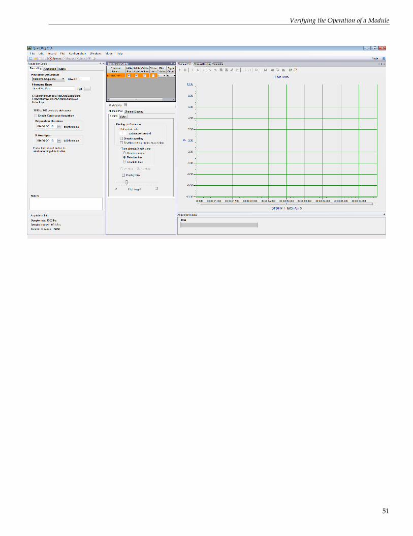
Acquire Data from an Analog Output ChannelThe following steps describe how to use the QuickDAQ application to monitor the output of the analog output signal using an analog input channel.
In this example, a 3 V sine wave is output on analog output channel 0 of a DT9847-1-1 module. The analog output channel is connected to analog input channel 0 on the DT9847-1-1 module.
Configure the Analog Output Settings
For this example, configure the analog output channel as follows:
1. Click the Output tab of the Acquisition and Config window.

Verifying the Operation of a Module
2. Select the Enable checkbox to enable the analog output channel on the module.
3. For the Waveform type, select Fixed.
4. For Peak Voltage, enter 3 to output a ±3 V signal.
5. For Offset, enter 0.
6. For Signal Type, select Sine to output a sine wave.
7. For Output Mode, select Continuous to output a waveform that repeats continuously.
8. For Frequency, select 10 Hz; this is the frequency of the output waveform.
9. For Ramp Up Time, enter 0.
10. For the Start/Stop Method, select With Acquisition.The analog output operation will start when you start acquisition.
11. If desired, hide the Acquisition Config window by clicking the Auto-Hide pin ( ) in the top, right corner of the window.
Configure the Analog Input Channel
Configure the analog input channel as follows:
1. Ensure that the output from analog output channel 0 is connected to the input of analog input channel 0.
2. Configure the analog input channel by clicking the Input Channel Configuration toolbar button ( ) or by clicking the Configuration menu and clicking Input Channel Configuration.
3. Enable analog input channel 0 by clicking the Enable checkbox next to the channel.
4. Under the Channel Name column, leave the default channel name as Ain 0.
5. Under the Range column, select the input range for analog input channel. In this example, ±10 V is used.
6. Under the Coupling column, select the coupling type (AC or DC) for your sensor. Since this example is monitoring a voltage input, DC is used.
53

Chapter 4
54
7. Under the Current Source column, select whether to enable or disable use of the 4 mA current source on the data acquisition device. Since this example is monitoring a voltage input, the Current Source checkbox is not checked (disabled) for the analog input channel.
8. Under the Engineering Units column, select the engineering units for the input.In this example, V is used.
9. Enter the number of mV per engineering unit in the mV/EU field.In this example, 1000 is used.
10. If an offset is specified for the input, enter the value in the EU Offset field.In this example, no offset (0) is specified.
11. If desired, enter a test point value for the channel. In this example, 0 is used.
12. If desired, enter a sensor direction for each channel. In this example, Scalar is used.
13. Click Close to close the Configure Devices dialog box.
Verifying the Operation of a Module
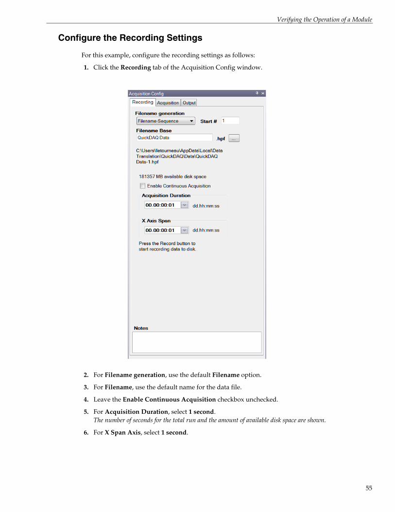
Configure the Recording Settings
For this example, configure the recording settings as follows:
1. Click the Recording tab of the Acquisition Config window.
2. For Filename generation, use the default Filename option.
3. For Filename, use the default name for the data file.
4. Leave the Enable Continuous Acquisition checkbox unchecked.
5. For Acquisition Duration, select 1 second.The number of seconds for the total run and the amount of available disk space are shown.
6. For X Span Axis, select 1 second.
55

Chapter 4
56
Configure the Acquisition Settings
For this example, configure the acquisition settings as follows:
1. Click the Acquisition tab of the Acquisition Config window.
2. For the Per Channel Sampling Frequency text box, enter 2000.The application snaps the value to closest sampling frequency. The sampling rate, sample interval, and number of scans are displayed.
3. For the Trigger Source check box, select Software to ensure that the measurement starts as soon as the Record button is clicked.

Verifying the Operation of a Module
Start the Operation
Once you have configured the channels and the application parameters, click the Record toolbar button ( ) or press the F5 key to start the operation.
Results similar to the following are displayed in the Channel Plot window, showing the output of analog output channel 0 as measured by analog input channel 0.
Note: Many additional options are provided in QuickDAQ for measuring and analyzing the data. Refer to the QuickDAQ User’s Manual for detailed information.
57

Chapter 4
58

Part 2: Using Your Module

5Principles of Operation
Analog Input Features . . . . . . . . . . . . . . . . . . . . . . . . . . . . . . . . . . . . . . . . . . . . . . . . . . . . . . . . . 64
Analog Output Features . . . . . . . . . . . . . . . . . . . . . . . . . . . . . . . . . . . . . . . . . . . . . . . . . . . . . . . 72
Digital I/O Features. . . . . . . . . . . . . . . . . . . . . . . . . . . . . . . . . . . . . . . . . . . . . . . . . . . . . . . . . . . 77
Triggering Acquisition on Multiple Modules . . . . . . . . . . . . . . . . . . . . . . . . . . . . . . . . . . . . . 78
Synchronizing Acquisition on Multiple DT9847 Series Modules . . . . . . . . . . . . . . . . . . . . . 79
61

Chapter 5
62
Figure 19 shows a block diagram of the DT9847-1-1 module.
Figure 19: Block Diagram of the DT9847-1-1 Module
Figure 20 shows a block diagram of a DT9847-2-2 module.
Figure 20: Block Diagram of the DT9847-2-2 Module
Ext. Trigger
Ain 0
24-Bit A/D
4 mA
+18 Volts
1 Mx1 / 10
AC - DC Coupling
USB 2.0 High Speed
Interface
USB 2.0A/D PLL
Programmable Clock
32-Bit D/A Converter
100 kHz Filter
15-pin Connector Digital In
Digital Out
D/A PLL Programmable
Clock
Control Logic
Sync Bus Clock & Trigger
RJ45
D/A Output 0
Ext. Trigger
Ain 0
24-Bit A/D
4 mA
+18 Volts
1 Mx1 / 10
AC - DC Coupling
USB 2.0 High Speed
Interface
USB 2.0A/D PLL
Programmable Clock
32-Bit D/A Converter
100 kHz Filter
15-pin Connector Digital In
Digital Out
D/A PLL Programmable
Clock
Control Logic RJ45
24-Bit A/D
4 mA
+18 Volts
1 Mx1 / 10
AC - DC Coupling
Ain 1
32-Bit D/A Converter
100 kHz Filter
D/A Output 1
Principles of Operation
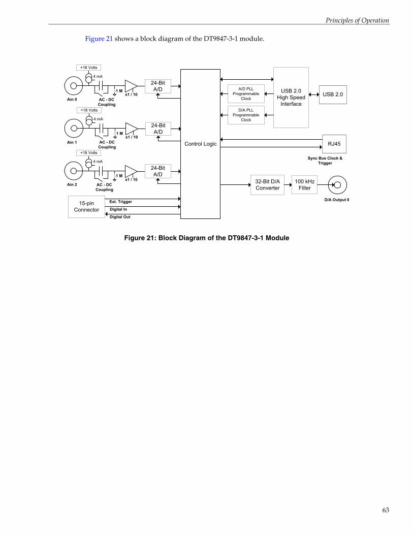
Figure 21 shows a block diagram of the DT9847-3-1 module.
Figure 21: Block Diagram of the DT9847-3-1 Module
D/A Output 0Ext. Trigger
Ain 0
24-Bit A/D
4 mA
+18 Volts
1 Mx1 / 10
AC - DC Coupling
USB 2.0 High Speed
Interface
USB 2.0A/D PLL
Programmable Clock
32-Bit D/A Converter
100 kHz Filter
15-pin Connector Digital In
Digital Out
D/A PLL Programmable
Clock
Control Logic
Sync Bus Clock & Trigger
RJ45
24-Bit A/D
4 mA
+18 Volts
1 Mx1 / 10
AC - DC Coupling
24-Bit A/D
4 mA
+18 Volts
1 Mx1 / 10
AC - DC Coupling
Ain 1
Ain 2
63

Chapter 5
64
Analog Input FeaturesThis section describes the following features of analog input (A/D) subsystem on the DT9847 Series modules:
• Analog input channels, described on this page
• IEPE functions, described on page 65
• Input resolution, described on page 65
• Input ranges and gains, described on page 64
• Input sample clock sources, described on page 65
• Analog input conversion modes, described on page 66
• Input triggers, described on page 69
• Data format and transfer, described on page 71
• Error conditions, described on page 71
Analog Input Channels
The DT9847-1-1 module provides one analog input channel (channel 0), the DT9847-2-2 provides two analog input channels (channels 0 and 1), and the DT9847-3-1 provides three analog input channels (channels 0 to 2). These are signal-ended channels; you can connect IEPE sensors to these inputs, if desired; refer to page 65 for more information on IEPE functions.
Note: To maintain simultaneous operation, all analog input connections on the DT9847 Series modules must have the same lead lengths.
The DT9847 Series modules use Delta-Sigma analog-to-digital converters (ADCs) that provide anti-aliasing filters based on the clock rate. These filters remove aliasing, which is a condition where high frequency input components erroneously appear as lower frequencies after sampling.
Using software, you can acquire a single value from a single analog input channel, a single value from all the analog input channels simultaneously (for the DT9847-2-2 and DT9847-3-1), or multiple values from a one or more analog input channels. Refer to “Analog Input Conversion Modes” on page 66 for more information on specifying and reading data from these channels.
Input Ranges and Gains
The DT9847 Series modules provide an input range of ±10 V and software-selectable gains of 1 and 10. This provides effective input ranges of ±10 V (when the gain is 1) and ±1 V (when the gain is 10).

Principles of Operation
IEPE Functions
Applications that require accelerometer, vibration, noise, or sonar measurements often use IEPE sensors. IEPE conditioning is built-in to the analog input circuitry of the DT9847 Series modules. The modules support the following software-programmable IEPE functions for each analog input channel:
• Excitation current source – The DT9847 Series modules provide an internal excitation current source of 4 mA. You can enable or disable the use of a internal excitation current source using software. By default, the excitation current source is disabled.
• Coupling type – You can select whether AC coupling or DC coupling is used. By default, DC coupling is selected for the DT9847 Series modules.
For information on wiring IEPE inputs, refer to page 40.
Note: If you enable the use of the internal excitation current source, it is recommended that you choose AC coupling.
Input Resolution
The resolution of the analog input channels is fixed at 24 bits; you cannot specify the resolution in software.
Input Clock Source
The DT9847 Series modules support a 48 MHz internal clock source, which is derived from the 24 MHz USB crystal oscillator. The same internal 48 MHz clock signal is used for the both the analog input and analog output subsystems.
For the analog input subsystem, use software to specify the internal clock source and the frequency at which to pace the input operations and to start the sample clock. The sampling frequency ranges from 1 kHz to 216 kHz.
Note: According to sampling theory (Nyquist Theorem), specify a frequency that is at least twice as fast as the input’s highest frequency component. For example, to accurately sample a 20 kHz signal, specify a sampling frequency of at least 40 kHz to avoid aliasing.
The sample frequencies for the A/D and D/A subsystems are independently programmable and are derived from the same 48 MHz reference clock. Therefore, it is possible to establish a fixed relationship between the A/D and D/A subsystem sample frequencies, including setting them to the same frequency (30 kHz to 216 kHz). However, the subsystems are not designed to be synchronous with each other.
65
Chapter 5
66
Once the sample clock is started, the module requires 63 conversions before the first A/D sample is valid. The valid sample is aligned with the A/D trigger.
On the DT9847 Series, the sampling frequency is generated by a programmable clock chip rather than a divider off the reference clock for better flexibility and accuracy.
Configuration Delay
Due to the design of the A/D converter on the DT9847 Series, you may notice a delay after you configure the sampling frequency on the module (when the Config command is called). The delay is more significant at slower sampling frequencies.
The configuration delay is determined as follows:
• Sampling rate 50 kHz:
Configuration delay = 8719 Samples/Sampling rate
• Sampling rate 100 kHz:
Configuration delay = 17423 Samples/Sampling rate
• Sampling rate 216 kHz:
Configuration delay = 34831 Samples/Sampling rate
For example, if you specify a sampling frequency of 1 kHz (sampling rate is 1 kSamples/s), the delay after you configure the sampling rate is 8.719 s, determined as follows:
8719 Samples/1 kSamples/s = 8.719 s
Similarly, if you specify a sampling frequency of 216 kHz (sampling rate is 216 kSamples/s), the delay after you configure the sampling rate is 0.161 s, determined as follows:
34831 Samples/216 kSamples/s = 0.161 s
Analog Input Conversion Modes
DT9847 Series modules support single-value, single-values, and continuous scan conversion modes. This section describes each of these conversion modes.
Single-Value Operations
Single-value operations are simpler to use than continuous operations. Using software, you specify the analog input channel and the gain that you want to use. For the DT9847-1-1, specify channel 0; for the DT9847-2-2, specify channel 0 or 1; for the DT9847-3-1, specify channel 0, 1, or 2. The module acquires the data from the specified channel and returns the data immediately.
For single-value operations, you cannot specify a clock source, trigger source, scan mode, or buffer. Single-value operations stop automatically when finished; you cannot stop a single-value operation.

Principles of Operation
Single-Values Operations
For the DT9847-2-2 or DT9847-3-1 module, you may prefer to read a single value from all the analog input channels simultaneously using one software call. This is called a single-values operation. You specify the analog input subsystem and the gain that you want to use for the channels (not the channels themselves). The module then acquires a value from each input channel simultaneously; the data is returned as an array of input values.
For single-values operations, you cannot specify a clock source, trigger source, scan mode, or buffer. Single-values operations stop automatically when finished; you cannot stop a single-values operation.
Continuous Scan Mode
Continuous scan mode takes full advantage of the capabilities of the DT9847 Series modules. You can specify a channel list, clock source, start trigger, reference trigger, post-trigger scan count, and buffer using software.
On the DT9847-1-1 module, you can enter up to one entry in the channel list (analog input channel 0). On the DT9847-2-2 module, you can enter up to two entries in the channel list (analog input channels 0 and 1). On the DT9847-3-1 module, you can enter up to three entries in the channel list (analog input channels 0 to 2). Using software, specify the channels you want to sample in sequential order.
When it detects the start trigger, the module samples all the channels in the list simultaneously.
If a reference trigger is not specified, data that is acquired after the start trigger is post-trigger data. The sampled data is placed in the allocated buffer(s). The operation continues until you stop it or until no more buffers are available.
If a reference trigger is specified, data that is acquired after the start trigger is pre-trigger data; when the reference trigger occurs, pre-trigger data acquisition stops and post-trigger acquisition starts at the next sample. The sampled data is placed in the allocated buffer(s). The operation continues until the number of scans that you specify for the post-trigger scan count have been acquired; at the point, the operation stops. Note that the sample at which the trigger occurs is not counted as a post-trigger sample. Refer to page 69 for more information about triggers.
The conversion rate is determined by the frequency of the input sample clock; refer to page 65 for more information about the input sample clock.
Using software, you can stop a scan by performing either an orderly stop or an abrupt stop. In an orderly stop, the module finishes acquiring the current buffer, stops all subsequent acquisition, and transfers the acquired data to host memory; any subsequent triggers are ignored. In an abrupt stop, the module stops acquiring samples immediately; the current buffer is not completely filled, it is returned to the application only partially filled, and any subsequent triggers are ignored.
67

Chapter 5
68
To select continuous scan mode, use software to specify the following parameters:
• Specify the data flow as Continuous
• Specify the clock source as internal and specify the clock frequency (refer to page 65)
• Specify the start trigger (refer to page 69)
• Specify the reference trigger (refer to page 70)
• Specify the post-trigger scan count (the number of post-trigger samples to acquire after the reference trigger occurs)
Figure 22 illustrates continuous scan mode (using a start and reference trigger) with a channel list of three entries: channel 0 through channel 2. In this example, pre-trigger analog input data is acquired when the start trigger is detected. When the reference trigger occurs, the specified number of post-trigger samples (3, in this example) are acquired.
Figure 22: Continuous Scan Mode on the DT9847 Series ModulesUsing a Start and Reference Trigger
Note: The USB LED, shown in Figure 34 on page 132, blinks amber while the module is acquiring data.
The Trigger LED on the module, shown in Figure 34 on page 132, is green when the module is waiting for an external digital trigger, threshold trigger, or Sync Bus trigger (the module must have been configured for one of these trigger types), green when the module has been triggered, or off when the module is idle.
Chan 0
Chan 1
Chan 2
Input Sample Clock
Chan 0
Chan 1
Chan 2
Chan 0
Chan 1
Chan 2
Chan 0
Chan 1
Chan 2
Start Trigger occurs Reference Trigger occurs
3 Post-trigger samples acquiredPre-trigger data acquired
Chan 0
Chan 1
Chan 2
Post-Trigger Scan Count = 3
Chan 0
Chan 1
Chan 2
Trigger Sample is not counted as post-trigger sample

Principles of Operation
Input Triggers
A trigger is an event that occurs based on a specified set of conditions.
On the DT9847 Series modules, you can specify a start trigger source and a reference trigger source. Pre-trigger data acquisition starts when the start trigger event occurs. When the reference trigger event occurs, pre-trigger data acquisition stops and post-trigger acquisition starts. Post-trigger acquisition stops when the number of samples you specify for the post-trigger scan count has been reached. Refer to page 67 for more information.
The Trigger LED on the module, shown in Figure 34 on page 132, is green when the module is waiting for an external digital trigger, threshold trigger, or Sync Bus trigger (the module must have been configured for one of these trigger types), red when the module has been triggered, or off when the module is idle.
Start Trigger Sources
The DT9847 Series modules support the following sources for the start trigger:
• Software trigger – A software trigger event occurs when you start the analog input operation (the computer issues a write to the module to begin conversions). Using software, specify the start trigger source as a software trigger.
• External digital (TTL) trigger – An external digital (TTL) trigger event occurs when the module detects a rising- or falling-edge transition on the signal connected to the External Trigger pin (pin 13) of the Digital I/O and External Trigger connector on the module. Using software, specify the trigger source as an external, positive digital (TTL) trigger to detect the trigger on the rising edge or an external, negative digital (TTL) trigger to detect the trigger on the falling edge.
Note: If you configure the synchronization mode as slave, the Sync Bus connector accepts trigger and clock signals from the master; you cannot use the Ext Trig connector on the slave module. Refer to page 79 for more information.
• Analog threshold trigger – The start trigger event occurs when the signal attached to a specified analog input channel in the channel list rises above or falls below a user-specified threshold value. Using software, specify the following parameters:
Start trigger source – Specify a positive (low-to-high transition) threshold trigger if you want to trigger when the signal rises above a threshold level, or a negative (high-to-low transition) threshold trigger if you want to trigger when the signal falls below a threshold level.
Threshold channel – Specify any one of the analog input channels that are included in the channel list as the threshold input channel.
Threshold level – Specify a value between ±10 V for a gain of 1 or ±1 V for a gain of 10 as the threshold level.
69
Chapter 5
70
Note: If you choose a threshold trigger as both the start trigger and the reference trigger, the threshold channel and threshold level must be the same. The polarity of the trigger (positive or negative going) can be different for each trigger source.
• Sync Bus trigger – When multiple DT9847 Series modules (or multiple DT9847 Series and DT9837 Series or DT9838 modules) are connected together using the Sync Bus (RJ45) connector, you can use the Sync Bus trigger as the start trigger of the slave module by setting the synchronization mode of module to Slave. In this configuration, any other start trigger for the slave module is ignored. Refer to page 79 for more information on this configuration.
Reference Trigger Sources
The DT9847 Series modules support the following sources for the reference trigger:
• External digital (TTL) trigger – The reference trigger event occurs when the module detects a rising- or falling-edge transition on the signal connected to the External Trigger pin (pin 13) of the Digital I/O and External Trigger connector on the module. Using software, specify the reference trigger source as an external, positive digital (TTL) trigger to detect the trigger on the rising edge or an external, negative digital (TTL) trigger to detect the trigger on the falling edge.
• Analog threshold trigger –The reference trigger event occurs when the signal attached to a specified analog input channel in the channel list rises above or falls below a user-specified threshold value. Using software, specify the following parameters:
Reference trigger source – Specify a positive (low-to-high transition) threshold trigger if you want to trigger when the signal rises above a threshold level, or a negative (high-to-low transition) threshold trigger if you want to trigger when the signal falls below a threshold level.
Threshold channel – Specify any one of the analog input channels that are included in the channel list as the threshold input channel.
Threshold level – Specify a value between ±10 V for a gain of 1 or ±1 V for a gain of 10 as the threshold level.
Note: If you choose a threshold trigger as both the start trigger and the reference trigger, the threshold channel and threshold level must be the same. The polarity of the trigger (positive or negative going) can be different for each trigger source.
• Sync Bus trigger – When multiple DT9847 Series modules (or multiple DT9847 Series and DT9837 Series or DT9838 modules) are connected together using the Sync Bus (RJ45) connector, you can set the reference trigger of a slave DT9847 Series module to Sync Bus if you want to receive a Sync Bus trigger from one of the other modules to stop pre-trigger acquisition and start post-trigger acquisition. Refer to page 79 for more information on this configuration.
Principles of Operation
Data Format and Transfer
DT9847 Series modules use offset binary data encoding, where 000000 represents negative full-scale, and FFFFFFh represents positive full-scale. Use software to specify the data encoding as binary. The ADC outputs FFFFFFh for above-range signals, and 000000 for below-range signals.
Before you begin acquiring data, you must allocate buffers to hold the data. A Buffer Done event is returned whenever a buffer is filled. This allows you to move and/or process the data as needed.
We recommend that you allocate a minimum of two buffers for continuous analog input operations. Data is written to multiple allocated input buffers continuously; when no more empty buffers are available, the operation stops. The data is gap-free.
Note: DT9847 Series modules have an 8 kSample input FIFO that is used to store the acquired data before it is sent to the host.
Error Conditions
DT9847 Series modules report any overrun errors by sending an overrun event to the application program. This event indicates that data buffers are not being sent from the module to the host fast enough, and the A/D converter ran out of buffers. To avoid this error, try one or more of the following:
• Reduce the clock rate of the A/D
• Increase the size of the buffers
• Increase the number of buffers
• Close any other applications that are running
• Run the program on a faster computer
If one of these error conditions occurs, the module stops acquiring and transferring data to the host computer.
71
Chapter 5
72
Analog Output FeaturesThis section describes the following features of analog output operations:
• Analog output channels, described below
• Output ranges and gains, described below
• Output resolution, described below
• Output clocks, described below
• Output conversion mode, described on page 73
• Output triggers, described on page 75
• Data format and transfer, described on page 76
• Error conditions, described on page 76
Analog Output Channels
The DT9847-1-1 and DT9847-3-1 modules support one analog output channel (0) through analog output subsystem 0. The DT9847-2-2 module supports two analog output channels (0 and 1) through analog output subsystem 0.
The DT9847 Series modules provide a two-pole, 250 kHz Butterworth filter to prevent noise from interfering with the output signal.
The analog output channel powers up to a value of 0 V ±10 mV.
Output Ranges and Gains
The DT9847 Series modules can output bipolar analog output signals in the range of ±3 V or ±10 V. The output range is software programmable. The gain is 1.
Note: Older versions of the module may support only the ±3 V range.
Output Resolution
The resolution of the analog output channel is fixed at 32-bits; you cannot specify the resolution in software.
Output Clocks
The DT9847 Series modules support a 48 MHz internal clock source, which is derived from the 24 MHz USB crystal oscillator. The same internal 48 MHz clock signal is used for the both the analog input and analog output subsystems.

Principles of Operation
For the analog output subsystem, use software to specify the internal clock source and the output frequency. The output frequency can range between 30 kHz and 216 kHz.
Note: The sample frequencies for the A/D and D/A subsystems are independently programmable and are derived from the same 48 MHz reference clock. Therefore, it is possible to establish a fixed relationship betwen the A/D and D/A subsystem sample frequencies, including setting them to the same frequency (30 kHz to 216 kHz). However, the subsystems are not designed to be synchronous with each other.
Due to the group delay of the Delta-Sigma D/A converter, the DT9847 Series modules require 36 clock pulses once the analog output sample clock is started before the first D/A conversion is completed.
Output Conversion Modes
The DT9847 Series modules support single-value, waveform, and continuous analog output operations.
Single-Value Mode
Single-value mode is the simplest to use but offers the least flexibility and efficiency. Use software to specify the analog output channel that you want to update, and the value to output from that channel. The value is output from the specified channel immediately.
For a single-value operation, you cannot specify a clock source, trigger source, or buffer. Single-value operations stop automatically when finished; you cannot stop a single-value operation.
Waveform Generation Mode
Waveform generation mode is supported on the DT9847 Series modules. In this mode, a waveform, which is specified in a single buffer, is output repetitively. The waveform pattern can range from 2 to 8192 samples if you are using one analog output channel or from 2 to 4096 if you are using two analog output channels. Use software to fill the output buffer with the values that you want to write to the channels in the output channel list.
Note: If you are using the DataAcq SDK, you must specify the data in a particular order. For example, if your output channel list contains analog output channels 0 and 1, specify the values in the output buffer as follows: the first output value for analog output channel 0, the first output value for analog output channel 1, the second output value for analog output channel 0, the second output value for analog output channel 1, and so on.
This is not required in the DT-Open Layers for .NET Class Library.
73
Chapter 5
74
The host computer transfers the entire waveform pattern to the 8 kSample output FIFO on the module. When it detects a software trigger, the module starts writing output values to the analog output channels at the specified clock rate. The module recycles the data, allowing you to output the same pattern continuously without any further CPU or USB bus activity.
When it reaches the end of the FIFO, the module returns to the first location of the FIFO and continues outputting the data. This process continues indefinitely until you stop it.
To select waveform generation mode, use software to specify the following parameters:
• Specify the data flow as Continuous
• Specify WrapSingleBuffer as True to use a single buffer
• Specify the clock source as internal and specify the clock frequency. Refer to page 72 for more information about the clock source and frequency.
• Specify a software trigger source, described in the next section
The DT9847 Series hardware supports the ability to mute the output voltage to 0 V. Muting the output does not stop the analog output operation; instead, the analog output voltage is reduced to 0 V over 1020 samples. When desired, you can use unmute the output voltage to its current level. Refer to your software documentation for more information on muting and unmuting the output voltage.
Continuous Analog Output Operations
Use continuously paced analog output mode to continuously output buffered values to the analog output channel at a specified clock frequency. The DT9847 Series modules support the ability to start continuous analog output operations and continuous analog input operations simultaneously.
Note: If you are using the DataAcq SDK, you must specify the data in a particular order. For example, if your output channel list contains analog output channels 0 and 1, specify the values in the output buffer as follows: the first output value for analog output channel 0, the first output value for analog output channel 1, the second output value for analog output channel 0, the second output value for analog output channel 1, and so on.
This is not required in the DT-Open Layers for .NET Class Library.
When it detects a trigger, the module starts writing the values from the output buffer to the channels specified in the output channel list at the specified clock frequency. The operation repeats continuously until all the data is output from the buffers or you stop the operation.
Note: Make sure that the host computer transfers data to the output channel list fast enough so that the list does not empty completely; otherwise, an underrun error results.

Principles of Operation
To select continuously paced analog output mode, use software to specify the following parameters:
• Specify the data flow as Continuous
• Specify WrapSingleBuffer as False to use multiple buffers
• Specify the clock source as internal and specify the clock frequency. Refer to page 72 for more information about the clock source and frequency.
• Specify the trigger source as any of the supported trigger sources. Refer to page 75 for more information about the supported trigger sources.
• To start the analog input and analog output operations simultaneously using the DT-Open Layers for .NET Class Library, use the SimultaneousStart.AddSubsystem, SimultaneousStart.PreStart, and SimultaneousStart.Start methods. Refer to the documentation for the DT-Open Layers for .NET Class Library for more information.
We recommend that you allocate a minimum of two buffers for a continuously paced analog output operation. Data is written from multiple output buffers continuously; when no more buffers of data are available, the operation stops. The data is gap-free.
Note: The USB LED, shown in Figure 34 on page 132, blinks amber while the module is streaming the data to the analog output channels in continuous mode.
The DT9847 Series hardware supports the ability to mute the output voltage to 0 V. Muting the output does not stop the analog output operation; instead, the analog output voltage is reduced to 0 V over 1020 samples. When desired, you can use unmute the output voltage to its current level. Refer to your software documentation for more information on muting and unmuting the output voltage.
To stop a continuously paced analog output operation, you can stop queuing buffers for the analog output system, letting the module stop when it runs out of data, or you can perform either an orderly stop or an abrupt stop using software. In an orderly stop, the module finishes outputting the specified number of samples, and then stops; all subsequent triggers are ignored. In an abrupt stop, the module stops outputting samples immediately; all subsequent triggers are ignored.
Output Trigger
The DT9847 Series modules support the following trigger sources for starting analog output operations:
• Software trigger – A software trigger event occurs when you start the analog output operation (the computer issues a write to the module to begin conversions). Using software, specify the trigger source for the D/A subsystem as a software trigger.
• External digital (TTL) trigger – An external digital (TTL) trigger event occurs when the module detects a rising- or falling-edge transition on the signal connected to the External Trigger pin (pin 13) of the Digital I/O and External Trigger connector on the module.
75
Chapter 5
76
Using software, specify the trigger source for the D/A subsystem as an external, positive digital (TTL) trigger or an external, negative digital (TTL) trigger.
Note: If you configure the synchronization mode as slave, the Sync Bus connector accepts trigger and clock signals from the master; you cannot use the Ext Trig connector on the slave module. Refer to page 79 for more information.
• Sync Bus trigger – When multiple DT9847 Series modules (or multiple DT9847 Series and DT9837 Series or DT9838 modules) are connected together using the Sync Bus (RJ45) connector, you can use the Sync Bus trigger as the start trigger of the slave module by setting the synchronization mode of module to Slave. In this configuration, any other start trigger for the slave module is ignored. Refer to page 79 for more information on this configuration.
Data Format and Transfer
Data from the host computer must use offset binary data encoding for analog output signals, where 00000000 represents the negative full-scale voltage, and FFFFFFFFh represents the positive full-scale voltage. Using software, specify the data encoding as binary.
Error Conditions
The DT9847 Series modules report any underrun errors by sending an underrun event to the application. This event indicates that the data buffers are not being sent from the host to the module fast enough, and the D/A converter ran out of data. To avoid this error, try one or more of the following:
• Reduce the clock rate of the analog output operation
• Close any other applications that are running
• Run the program on a faster computer

Principles of Operation
Digital I/O FeaturesThis section describes the following features of digital I/O operations:
• Digital I/O lines, described below
• Operation modes, described below
Digital I/O Lines
The DT9847 Series modules support one digital input port, consisting of 4 digital input lines (lines 0 to 3) and one digital output port, consisting of 4 digital output lines (lines 0 to 3). The resolution is fixed at 4 bits; you cannot change the resolution in software.
You can read all 4 digital input lines or write all 4 digital output lines with a single-value digital I/O operation.
A digital line is high if its value is 1; a digital line is low if its value is 0. On power up or reset, a low value (0) is output from each of the digital output lines.
Operation Modes
The DT9847 Series modules support single-value digital I/O operations. You use software to specify the digital I/O port (the gain is ignored). Data is then read from or written to all the digital I/O lines.
Single-value operations stop automatically when finished; you cannot stop a single-value operation.
77
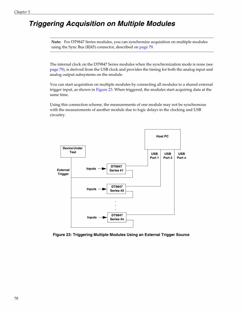
Chapter 5
78
Triggering Acquisition on Multiple Modules
Note: For DT9847 Series modules, you can synchronize acquisition on multiple modules using the Sync Bus (RJ45) connector, described on page 79.
The internal clock on the DT9847 Series modules when the synchronization mode is none (see page 79), is derived from the USB clock and provides the timing for both the analog input and analog output subsystems on the module.
You can start acquisition on multiple modules by connecting all modules to a shared external trigger input, as shown in Figure 23. When triggered, the modules start acquiring data at the same time.
Using this connection scheme, the measurements of one module may not be synchronous with the measurements of another module due to logic delays in the clocking and USB circuitry.
Figure 23: Triggering Multiple Modules Using an External Trigger Source
Host PC
DT9847 Series #1
USB Port 1
DT9847 Series #2
USB Port 2
DT9847 Series #n
USB Port n
.
.
.
Device Under Test
ExternalTrigger
Inputs
Inputs
Inputs

Principles of Operation
Synchronizing Acquisition on Multiple DT9847 Series Modules
DT9847 Series modules provide a Sync Bus (RJ45) connector that you can use to connect and synchronize multiple DT9847 Series modules.
Note: Note that you can also connect DT9837A, DT9837B, DT9837C, and/or DT9838 modules to a DT9847 Series module in this configuration. Refer to the DT9837 Series User’s Manual and the DT9838 User’s Manual for more information.
In this scheme, one module is the master and the other modules are the slave. You specify the synchronization mode (master, slave, or none) of the A/D subsystem using software.
When configured as a master, the Sync Bus connector outputs trigger and clock signals. When configured as a slave, the Sync Bus connector accepts trigger and clock signals from the master; the start trigger source on the slave module in is ignored in this configuration since the Sync Bus is used as the start trigger. When configured as none (the default mode), the DT9847 Series module uses the USB clock instead of the Sync Bus connector. The synchronization mode remains set until changed or until the application exits.
You can connect multiple modules in one of two ways. Figure 24 shows how to connect a maximum of two DT9847 Series modules by daisy chaining them together through the Sync Bus connector. Figure 25 shows how to connect a maximum of four DT9847 Series modules by using an RJ45 distribution panel, such as the EP386, where the panel contains four RJ45 connectors that are wired in parallel.
Figure 24: Synchronizing Two DT9847 Series Modules by Daisy Chaining the Sync Bus Connectors
Host PC
DT9847 Series Master
MasterSynchronization Mode is Master.
Start Trigger can be Software, External Digital Trigger, or Threshold Trigger.
Reference Trigger can be External Digital Trigger or Threshold Trigger.
Sync Bus (RJ45)
DT9847 Series Slave
USB Port 2
USB Port 1
USB
USB
SlaveSynchronization Mode is Slave.
Start Trigger is ignored (Sync Bus is used).
Reference Trigger can be External Digital Trigger, Threshold Trigger, or Sync Bus. (Sync Bus is generally used in this configuration.)
Device Under Test
Inputs
Inputs
79

Chapter 5
80
Figure 25: Synchronizing Four DT9847 Series Modules Using the EP386 RJ45 Distribution Panel (Shown Using an External Trigger)
When synchronizing multiple modules, start the slave modules before starting the master module. When the master DT9847 Series module is triggered (using the software trigger, external digital trigger, or threshold trigger), both the master and the slave modules start acquiring data at the same time (within one A/D conversion of the clock). Note that you can set the clock rate to be the same or different on each module.
DT9847 Series Master
Sync Bus
USB Port 2
DT9847 Series Slave
Host PC
USB Port 1
DT9847 SeriesSlave
DT9847 SeriesSlave
USB Port 3
USB Port 4
Sync Bus
Sync Bus
Sync Bus
USB
USB
USB
USB
EP386RJ45 Distribution Panel (connectors wired
* The RJ45 cables must be less than 1 foot in length. For minimum clock skew, the master module must be less than 4 inches away from the RJ45 distribution panel.
MasterSynchronization Mode is Master.
Start Trigger can be Software, External Digital Trigger, or Threshold Trigger.
Reference Trigger can be External Digital Trigger, or Threshold Trigger.
SlaveSynchronization Mode is Slave.
Start Trigger is ignored (Sync Bus is used).
Reference Trigger can be External Digital Trigger, Threshold Trigger, or Sync Bus. (Sync Bus is generally used in this
Device Under Test
Inputs
Inputs
Inputs
Inputs
Principles of Operation
Note: It is important that you start the slave modules first, followed by the master module so that the slave receives the appropriate clock and trigger signals from the master.
If you start the master module before the slaves, the slaves never start; you will see a delay of approximately 20 seconds if you try to stop or abort the analog input operation on a slave module that is waiting for a trigger.
When you stop the master module, the slaves continue to run and return data until you stop the analog input subsystem on the slave modules. Be sure to stop the analog input subsystems on all slave modules before disconnecting the cable from the Sync Bus connectors.
Triggering DT9847 and DT9837 Series Modules Using the Sync Bus
If you are connecting the DT9847 Series module to a DT9837 Series module using the Sync Bus connector, be aware of triggering limitations.
Note: There are no triggering limitations when connecting a DT9847 Series module to a DT9838 module using the Sync Bus connector; follow the instructions on page 80 when connecting a DT9838 module.
The DT9837 Series supports the following start trigger sources: software, external digital trigger, and threshold trigger. For the reference trigger, the DT9837 Series supports only the threshold trigger source. When configured as a slave, the DT9837 Series processes a single Sync Bus trigger; the Sync Bus trigger is considered the start trigger and is received and/or driven out as such.
Consider the case where the DT9847 Series module is the master and a DT9837 Series module is the slave, as shown in Figure 26.
81

Chapter 5
82
Figure 26: Synchronizing a Master DT9847 Series Module and a Slave DT9837 Series Module Using the Sync Bus Connector
In this case, the start trigger on the master DT9847 Series module can be a software trigger, external digital trigger, or threshold trigger. The reference trigger on the master DT9847 Series module can be an external digital trigger or threshold trigger.
The start trigger on the slave DT9837 Series module is ignored, since the Sync Bus is used as the start trigger. The reference trigger on the slave DT9837 Series can be the threshold trigger, or you can use software to stop the DT9837 Series module and correlate the data.
Now, consider the case where the DT9837 Series is the master and a DT9847 Series module is the slave, as shown in Figure 27.
Host PC
DT9847 SeriesMaster
Device Under Test
DT9847 Series MasterSynchronization Mode is Master.
Start Trigger can be Software, External Digital Trigger, or Threshold Trigger.
Reference Trigger can be External Digital Trigger, or Threshold Trigger.
Inputs
Sync Bus (RJ45)
DT9837 SeriesSlaveInputs
USB Port 2
USB Port 1
USB
USB
DT9837 Series SlaveSynchronization Mode is Slave.
Start Trigger is ignored (Sync Bus is used).
Reference Trigger can be Threshold trigger, or you can use software to stop the slave and correlate the data.
Principles of Operation
Figure 27: Synchronizing a Master DT9837 Series Module and a Slave DT9847 Series Module Using the Sync Bus Connector
In this case, the start trigger on the master DT9837 Series module can be a software, external digital, or threshold trigger. The reference trigger on the master DT9837 Series module can be the threshold trigger.
The start trigger on the slave DT9847 Series module is ignored, since the Sync Bus is used as the start trigger. The reference trigger on the slave DT9847 Series module can be an external digital trigger or threshold trigger (the Sync Bus trigger is not supported as a reference trigger in this configuration), or you can use software to stop the DT9847 Series module and correlate the data.
Host PC
DT9837 Series Master
Device Under Test
DT9837 Series MasterSynchronization Mode is Master.
Start Trigger can be Software, External Digital Trigger, or Threshold Trigger.
Reference Trigger can be Threshold, or you can use software to stop the master.
Inputs
Sync Bus (RJ45)
DT9847 Series SlaveInputs
USB Port 2
USB Port 1
USB
USB
DT9847 Series SlaveSynchronization Mode is Slave.
Start Trigger is ignored (Sync Bus is used).
Reference Trigger can be External Digital Trigger, or Threshold Trigger, or you can use software to stop the slave and correlate the data.
83

Chapter 5
84
6Supported Device Driver Capabilities
Data Flow and Operation Options. . . . . . . . . . . . . . . . . . . . . . . . . . . . . . . . . . . . . . . . . . . . . . . 87
Buffering . . . . . . . . . . . . . . . . . . . . . . . . . . . . . . . . . . . . . . . . . . . . . . . . . . . . . . . . . . . . . . . . . . . . 88
Triggered Scan Mode. . . . . . . . . . . . . . . . . . . . . . . . . . . . . . . . . . . . . . . . . . . . . . . . . . . . . . . . . . 88
Data Encoding. . . . . . . . . . . . . . . . . . . . . . . . . . . . . . . . . . . . . . . . . . . . . . . . . . . . . . . . . . . . . . . . 88
Channels . . . . . . . . . . . . . . . . . . . . . . . . . . . . . . . . . . . . . . . . . . . . . . . . . . . . . . . . . . . . . . . . . . . . 89
Gain . . . . . . . . . . . . . . . . . . . . . . . . . . . . . . . . . . . . . . . . . . . . . . . . . . . . . . . . . . . . . . . . . . . . . . . . 89
Ranges . . . . . . . . . . . . . . . . . . . . . . . . . . . . . . . . . . . . . . . . . . . . . . . . . . . . . . . . . . . . . . . . . . . . . . 90
Resolution . . . . . . . . . . . . . . . . . . . . . . . . . . . . . . . . . . . . . . . . . . . . . . . . . . . . . . . . . . . . . . . . . . . 90
Current and Resistance Support . . . . . . . . . . . . . . . . . . . . . . . . . . . . . . . . . . . . . . . . . . . . . . . . 90
Thermocouple, RTD, and Thermistor Support . . . . . . . . . . . . . . . . . . . . . . . . . . . . . . . . . . . . 91
IEPE Support. . . . . . . . . . . . . . . . . . . . . . . . . . . . . . . . . . . . . . . . . . . . . . . . . . . . . . . . . . . . . . . . . 92
Bridge and Strain Gage Support . . . . . . . . . . . . . . . . . . . . . . . . . . . . . . . . . . . . . . . . . . . . . . . . 92
Start Triggers. . . . . . . . . . . . . . . . . . . . . . . . . . . . . . . . . . . . . . . . . . . . . . . . . . . . . . . . . . . . . . . . . 93
Reference Triggers . . . . . . . . . . . . . . . . . . . . . . . . . . . . . . . . . . . . . . . . . . . . . . . . . . . . . . . . . . . . 94
Clocks . . . . . . . . . . . . . . . . . . . . . . . . . . . . . . . . . . . . . . . . . . . . . . . . . . . . . . . . . . . . . . . . . . . . . . . 95
Counter/Timers . . . . . . . . . . . . . . . . . . . . . . . . . . . . . . . . . . . . . . . . . . . . . . . . . . . . . . . . . . . . . . 96
Tachometers . . . . . . . . . . . . . . . . . . . . . . . . . . . . . . . . . . . . . . . . . . . . . . . . . . . . . . . . . . . . . . . . . 97
85
Chapter 6
86
The DT9847 Series Device Drivers provide support for the analog input (A/D) and analog output (D/A) subsystems. For information on how to configure the device drivers, refer to page 36.
The tables in this chapter summarize the features available for use with the DT-Open Layers for .NET Class Library and the DT9847 Series modules. The DT-Open Layers for .NET Class Library provides properties that return support information for specified subsystem capabilities.
The first row in each table lists the subsystem types. The first column in each table lists all possible subsystem capabilities. A description of each capability is followed by the property used to describe that capability in the DT-Open Layers for .NET Class Library.
Note: The following tables include the capabilities that can be queried. However, some capabilities may not be supported by your device. Blank fields represent unsupported options.
For more information, refer to the description of these properties in the DT-Open Layers for .NET Class Library online help or DT-Open Layers for .NET Class Library User’s Manual.
Table 2: DT9847 Series Subsystems
DT9847 Series Modules A/D D/A DIN DOUT C/T TACH QUAD
Total Subsystems on Module 1 1 1 1 0 0 0

Supported Device Driver Capabilities
Data Flow and Operation Options
Table 3: Data Flow and Operation Options
DT9847 Series Modules A/D D/A DIN DOUT C/T TACH QUAD
Single-Value Operation SupportSupportsSingleValue Yes Yes Yes Yes
Simultaneous Single-Value Output OperationsSupportsSetSingleValues
Continuous Operation SupportSupportsContinuous Yes Yes
Continuous Operation until TriggerSupportsContinuousPreTrigger
Continuous Operation before & after TriggerSupportsContinuousPrePostTrigger
Waveform Operations Using FIFO OnlySupportsWaveformModeOnly Yesa
a. The DT9847 Series modules support continuous analog output operations in addition to waveform mode.
Simultaneous Start List SupportSupportsSimultaneousStart Yesb
b. The DT9847 Series modules support the ability to start continuous A/D and continuous D/A operations simultaneously.
Yesb
Supports Programmable Synchronization ModesSupportsSynchronization Yes
Synchronization ModesSynchronizationMode
None, Master, Slave
Interrupt SupportSupportsInterruptOnChange
FIFO Size, in samplesFifoSize 8 kSamples 8 kSamples
Muting and Unmuting the Output VoltageSupportsMute Yes
Auto-Calibrate SupportSupportsAutoCalibrate
87

Chapter 6
88
Buffering
Triggered Scan Mode
Data Encoding
Table 4: Buffering Options
DT9847 Series Modules A/D D/A DIN DOUT C/T TACH QUAD
Buffer SupportSupportsBuffering Yes Yes
Single Buffer Wrap Mode SupportSupportsWrapSingle Yes Yes
Inprocess Buffer Flush SupportSupportsInProcessFlush Yes
Table 5: Triggered Scan Mode Options
DT9847 Series Modules A/D D/A DIN DOUT C/T TACH QUAD
Triggered Scan SupportSupportsTriggeredScan
Maximum Number of CGL Scans per TriggerMaxMultiScanCount 1 0 0 0 0 0
Maximum Retrigger FrequencyMaxRetriggerFreq 0 0 0 0 0 0
Minimum Retrigger FrequencyMinRetriggerFreq 0 0 0 0 0 0
Table 6: Data Encoding Options
DT9847 Series Modules A/D D/A DIN DOUT C/T TACH QUAD
Binary Encoding SupportSupportsBinaryEncoding Yes Yes Yes Yes
Twos Complement SupportSupportsTwosCompEncoding
Returns Floating-Point ValuesReturnsFloats
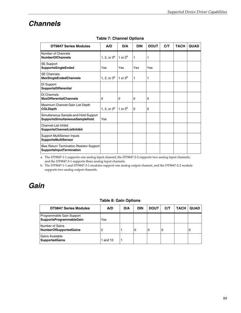
Supported Device Driver Capabilities
Channels
Gain
Table 7: Channel Options
DT9847 Series Modules A/D D/A DIN DOUT C/T TACH QUAD
Number of ChannelsNumberOfChannels 1, 2, or 3a
a. The DT9847-1-1 supports one analog input channel; the DT9847-2-2 supports two analog input channels; and the DT9847-3-1 supports three analog input channels.
1 or 2b
b. The DT9847-1-1 and DT9847-3-1 modules support one analog output channel, and the DT9847-2-2 module supports two analog output channels.
1 1
SE SupportSupportsSingleEnded Yes Yes Yes Yes
SE ChannelsMaxSingleEndedChannels 1, 2, or 3a 1 or 2b 1 1
DI SupportSupportsDifferential
DI ChannelsMaxDifferentialChannels 0 0 0 0
Maximum Channel-Gain List DepthCGLDepth 1, 2, or 3a 1 or 2b 0 0
Simultaneous Sample-and-Hold SupportSupportsSimultaneousSampleHold Yes
Channel-List InhibitSupportsChannelListInhibit
Support MultiSensor InputsSupportsMultiSensor
Bias Return Termination Resistor SupportSupportsInputTermination
Table 8: Gain Options
DT9847 Series Modules A/D D/A DIN DOUT C/T TACH QUAD
Programmable Gain SupportSupportsProgrammableGain Yes
Number of GainsNumberOfSupportedGains 2 1 0 0 0 0
Gains AvailableSupportedGains 1 and 10 1
89

Chapter 6
90
Ranges
Resolution
Current and Resistance Support
Table 9: Range Options
DT9847 Series Modules A/D D/A DIN DOUT C/T TACH QUAD
Number of Voltage RangesNumberOfRanges 1 1 0 0
Available RangesSupportedVoltageRanges ±10 Va
a. By applying a gain of 1, the effective input range is ±10 V. By applying a gain of 10, the effective input range is ±1 V.
±3 V or ±10 Vb
b. Software-programmable. Older versions of the module may support only the ±3 V range.
Table 10: Resolution Options
DT9847 Series Modules A/D D/A DIN DOUT C/T TACH QUAD
Software Programmable ResolutionSupportsSoftwareResolution
Number of ResolutionsNumberOfResolutions 1 1 1 1
Available ResolutionsSupportedResolutions 24 32 4 4
Table 11: Current and Resistance Support Options
DT9847 Series A/D D/A DIN DOUT C/T TACH QUAD
Current SupportSupportsCurrent
Current Output SupportSupportsCurrentOutput
Resistance SupportSupportsResistance
Software Programmable External Excitation Current Source for ResistanceSupportsExternalExcitationCurrentSrc
Software Programmable Internal Excitation Current SourceSupportsInternalExcitationCurrentSrc
Available Excitation Current Source Values SupportedExcitationCurrentValues

Supported Device Driver Capabilities
Thermocouple, RTD, and Thermistor Support
Table 12: Thermocouple, RTD, and Thermistor Support Options
DT9847 Series A/D D/A DIN DOUT C/T TACH QUAD
Thermocouple SupportSupportsThermocouple
RTD SupportSupportsRTD
Thermistor SupportSupportsThermistor
Voltage Converted to TemperatureSupportsTemperatureDataInStream
Supported Thermocouple TypesThermocoupleType
Supports CJC Source Internally in HardwareSupportsCjcSourceInternal
Supports CJC ChannelSupportsCjcSourceChannel
Available CJC ChannelsCjcChannel
Supports Interleaved CJC Values in Data StreamSupportsInterleavedCjcTemperaturesInStream
Supported RTD TypesRTDType
RTD R0 CoefficientRtdR0
Supports Data FiltersSupportsTemperatureFilters
Temperature Filter TypesTemperatureFilterType
91

Chapter 6
92
IEPE Support
Bridge and Strain Gage Support
Table 13: IEPE Support Options
DT9847 Series A/D D/A DIN DOUT C/T TACH QUAD
IEPE SupportSupportsIEPE Yes
Software Programmable AC CouplingSupportsACCoupling Yes
Software Programmable DC CouplingSupportsDCCoupling Yes
Software Programmable External Excitation Current SourceSupportsExternalExcitationCurrentSrc
Software Programmable Internal Excitation Current SourceSupportsInternalExcitationCurrentSrc Yes
Available Excitation Current Source ValuesSupportedExcitationCurrentValues .004 A
Table 14: Bridge and Strain Gage Support Options
DT9847 Series A/D D/A DIN DOUT C/T TACH QUAD
Bridge SupportSupportsBridge
Supported Bridge ConfigurationsBridgeConfiguration
Strain Gage SupportSupportsStrainGage
Supported Strain Gage Bridge ConfigurationsStrainGageBridgeConfiguration
External Excitation VoltageSupportsExternalExcitationVoltage
Internal Excitation VoltageSupportsInternalExcitationVoltage
Shunt CalibrationSupportsShuntCalibration
Voltage Excitation Per ChannelSupportedPerChannelVoltageExcitation
Minimum Excitation VoltageMinExcitationVoltage
Maximum Excitation VoltageMaxExcitationVoltage

Supported Device Driver Capabilities
Start Triggers
Table 15: Start Trigger Options
DT9847 Series A/D D/A DIN DOUT C/T TACH QUAD
Software Trigger SupportSupportsSoftwareTrigger Yes Yes Yes Yes
External Positive TTL Trigger SupportSupportsPosExternalTTLTrigger Yes Yes
External Negative TTL Trigger SupportSupportsNegExternalTTLTrigger Yes Yes
External Positive TTL Trigger Support for Single-Value OperationsSupportsSvPosExternalTTLTrigger
External Negative TTL Trigger Support for Single-Value OperationsSupportsSvNegExternalTTLTrigger
Positive Threshold Trigger SupportSupportsPosThresholdTrigger Yesa
a. If you choose a threshold trigger for the start trigger on the DT9847 Series module, you can program the threshold level as a value between ±10 V for a gain of 1 or ±1 V for a gain of 10, and any of the supported analog input channels can be used as the threshold channel.
Negative Threshold Trigger SupportSupportsNegThresholdTrigger Yesa
Digital Event Trigger SupportSupportsDigitalEventTrigger
Threshold Trigger ChannelSupportedThresholdTriggerChannel
0 (DT9847-1-1),0 or 1 (DT9847-2-2,0, 1, 2 (DT9847-3-1)a 0
93

Chapter 6
94
Reference Triggers
Table 16: Reference Trigger Options
DT9847 Series A/D D/A DIN DOUT C/T TACH QUAD
External Positive TTL Trigger SupportSupportsPosExternalTTLTrigger Yes
External Negative TTL Trigger SupportSupportsNegExternalTTLTrigger Yes
Positive Threshold Trigger SupportSupportsPosThresholdTrigger Yesa
a. If you choose a threshold trigger for the reference trigger on the DT9847 Series module, you can program the threshold level as a value between ±10 V for a gain of 1 or ±1 V for a gain of 10, and any of the supported analog input channels can be used as the threshold channel.
Negative Threshold Trigger SupportSupportsNegThresholdTrigger Yesa
Digital Event Trigger SupportSupportsDigitalEventTrigger
Sync Bus SupportSupportsSyncBusTrigger
Threshold Trigger ChannelSupportedThresholdTriggerChannel
0 (DT9847-1-1),0 or 1 (DT9847-2-2,0, 1, 2 (DT9847-3-1)a
Post-Trigger Scan CountlSupportsPostTriggerScanCount Yesb
b. You can specify how many post-trigger samples to acquire after the reference trigger by specifying the post-trigger scan count in software.

Supported Device Driver Capabilities
Clocks
Table 17: Clock Options
DT9847 Series A/D D/A DIN DOUT C/T TACH QUAD
Internal Clock SupportSupportsInternalClock Yes Yes
External Clock SupportSupportsExternalClock
Simultaneous Input/Output on a SingleClock Signal SupportsSimultaneousClocking Yes
Base Clock FrequencyBaseClockFrequency 13.824 MHz 27.648 MHz 0 0
Maximum Clock DividerMaxExtClockDivider 1.0 1.0 1.0 1.0
Minimum Clock DividerMinExtClockDivider 1.0 1.0 1.0 1.0
Maximum FrequencyMaxFrequency 216 kHz 216 kHz 0 0
Minimum FrequencyMinFrequency 1 kHz 30 kHz 0 0
95

Chapter 6
96
Counter/Timers
Table 18: Counter/Timer Options
DT9847 Series A/D D/A DIN DOUT C/T TACH QUAD
Cascading SupportSupportsCascading
Event Count Mode SupportSupportsCount
Generate Rate Mode SupportSupportsRateGenerate
One-Shot Mode SupportSupportsOneShot
Repetitive One-Shot Mode SupportSupportsOneShotRepeat
Up/Down Counting Mode SupportSupportsUpDown
Edge-to-Edge Measurement Mode SupportSupportsMeasure
Continuous Edge-to-Edge Measurement Mode Support SupportsContinuousMeasure
High to Low Output Pulse SupportSupportsHighToLowPulse
Low to High Output Pulse SupportSupportsLowToHighPulse
Variable Pulse Width SupportSupportsVariablePulseWidth
None (internal) Gate Type SupportSupportsGateNone
High Level Gate Type SupportSupportsGateHighLevel
Low Level Gate Type SupportSupportsGateLowLevel
High Edge Gate Type SupportSupportsGateHighEdge
Low Edge Gate Type SupportSupportsGateLowEdge
Level Change Gate Type SupportSupportsGateLevel
Clock-Falling Edge TypeSupportsClockFalling
Clock-Rising Edge TypeSupportsClockRising
Gate-Falling Edge TypeSupportsGateFalling
Gate-Rising Edge TypeSupportsGateRising
Interrupt-Driven OperationsSupportsInterrupt

Supported Device Driver Capabilities
Tachometers
Table 19: Tachometer Options
DT9847 Series A/D D/A DIN DOUT C/T TACH QUAD
Tachometer Falling EdgesSupportsFallingEdge
Tachometer Rising EdgesSupportsRisingEdge
Tachometer Stale Data FlagSupportsStaleDataFlag
97

Chapter 6
98
7Troubleshooting
General Checklist . . . . . . . . . . . . . . . . . . . . . . . . . . . . . . . . . . . . . . . . . . . . . . . . . . . . . . . . . . . . 100
Technical Support. . . . . . . . . . . . . . . . . . . . . . . . . . . . . . . . . . . . . . . . . . . . . . . . . . . . . . . . . . . . 102
If Your Module Needs Factory Service . . . . . . . . . . . . . . . . . . . . . . . . . . . . . . . . . . . . . . . . . . 103
99

Chapter 7
100
General ChecklistShould you experience problems using a DT9847 Series module, do the following:
1. Read all the documentation provided for your product, including any "Read this First" information.
2. Check the DT Omni software for any README files and ensure that you have used the latest installation and configuration information available.
3. Check that your system meets the requirements stated on page 30.
4. Check that you have installed your hardware properly using the instructions inChapter 2.
5. Check that you have installed and configured the device driver for your module using the instructions in Chapter 2.
6. Check that you have wired your signals properly using the instructions in Chapter 3.
7. Search the Knowledgebase in the Support section of the web site (at www.mccdaq.com) for an answer to your problem.
If you still experience problems, try using the information in Table 20 to isolate and solve the problem. If you cannot identify the problem, refer to page 102.
Table 20: Troubleshooting Problems
Symptom Possible Cause Possible Solution
Module is not recognized
You plugged the module into your computer before installing the device driver.
From the Control Panel > System > Hardware > Device Manager, uninstall any unknown devices (showing a yellow question mark). Then, run the DT Omni setup program to install the USB device drivers, and reconnect your USB module to the computer.
Module does not respond
The module configuration is incorrect. Check the configuration of your device driver; see the instructions in Chapter 2.
The module is damaged. Contact Data Translation for technical support; refer to page 102.
Intermittent operation
Loose connections or vibrations exist. Check your wiring and tighten any loose connections or cushion vibration sources; see the instructions in Chapter 3.
The module is overheating. Check environmental and ambient temperature; consult the module’s specifications on page 122 of this manual and the documentation provided by your computer manufacturer for more information.
Electrical noise exists. Check your wiring and either provide better shielding or reroute unshielded wiring; see the instructions in Chapter 3.

Troubleshooting
Device failure error reported
The DT9847 Series module cannot communicate with the Microsoft bus driver or a problem with the bus driver exists.
Check your cabling and wiring and tighten any loose connections; see the instructions in Chapter 3.
The DT9847 Series module was removed while an operation was being performed.
Ensure that your module is properly connected; see the instructions in Chapter 2.
Data appears to be invalid
An open connection exists. Check your wiring and fix any open connections; see the instructions in Chapter 3.
A transducer is not connected to the channel being read.
Check the transducer connections; see the instructions in Chapter 3.
The module is set up for differential inputs while the transducers are wired as single-ended inputs or vice versa.
Check your wiring and ensure that what you specify in software matches your hardware configuration; see the instructions in Chapter 3.
The module is out of calibration. DT9847 Series modules are calibrated at the factory. If you want to readjust the calibration of the analog input or analog output circuitry, refer to Chapter 8.
USB 2.0 is not recognized
Your operating system does not have the appropriate Service Pack installed.
Ensure that you load the appropriate Windows Service Pack. If you are unsure of whether you are using USB 2.0 or USB 1.1, run the Open Layers Control Panel applet, described in Chapter 2.
Standby mode is enabled on your PC. For some PCs, you may need to disable standby mode on your system for proper USB 2.0 operation. Consult Microsoft for more information.
Table 20: Troubleshooting Problems (cont.)
Symptom Possible Cause Possible Solution
101

Chapter 7
102
Technical Support If you have difficulty using a DT9847 Series module, Data Translation’s Technical Support Department is available to provide technical assistance.
To request technical support, go to our web site at http://www.mccdaq.com and click on the Support link.
When requesting technical support, be prepared to provide the following information:
• Your product serial number
• The hardware/software product you need help on
• The version of the Omni software that you are using
• Your contract number, if applicable
If you are located outside the USA, contact your local distributor; see our web site (www.mccdaq.com) for the name and telephone number of your nearest distributor.

Troubleshooting
If Your Module Needs Factory Service Most hardware models can be functionally tested, evaluated for repairs (if needed), and calibrated to factory specifications. An RMA# must be obtained from Applications Engineering in advance of sending any product back to Measurement Computing (Data Translation is a Measurement Computing company). Customers outside the USA must contact their local distributor for a return procedure. Calibration certificates for most analog models can be obtained for a fee (certificate must be requested at time of RMA# assignment).
103

Chapter 7
104
8Calibration
Using the Calibration Utility . . . . . . . . . . . . . . . . . . . . . . . . . . . . . . . . . . . . . . . . . . . . . . . . . . 107
Calibrating the Analog Input Subsystem . . . . . . . . . . . . . . . . . . . . . . . . . . . . . . . . . . . . . . . . 108
Calibrating the Analog Output Subsystem . . . . . . . . . . . . . . . . . . . . . . . . . . . . . . . . . . . . . . 110
105

Chapter 8
106
DT9847 Series modules are calibrated at the factory and should not require calibration for initial use. We recommend that you check and, if necessary, readjust the calibration of the analog input and analog output circuitry every six months using the DT9847 Series Calibration Utility.
Note: Ensure that you installed the device driver for your module using the Omni software prior to using the calibration utility.
This chapter describes how to calibrate the analog input and output subsystems of a DT9847 Series module using the calibration utility.

Calibration
Using the Calibration UtilityStart the DT9847 Series Calibration Utility as follows:
1. Click Start from the Task Bar.
2. For the DT9847 module, select Programs | Data Translation, Inc | Calibration | DT9847 Series Calibration Utility.The main window of the DT9847 Series Calibration Utility appears.
3. Select the module to calibrate, and then click OK.
Note: When you first run the DT9847 Series Calibration Utility, you may notice a delay before you can start using the utility. This is the configuration delay that is related to the sampling frequency, as described on page 66.
Once the calibration utility is running, you can calibrate the analog input circuitry (either automatically or manually), described on page 108, or the analog output circuitry of the module, described on page 110.
107

Chapter 8
108
Calibrating the Analog Input Subsystem This section describes how to use the calibration utility to calibrate the analog input subsystem of a DT9847 Series module.
DT9847 Series modules have separate calibration for each A/D input channel.
Warming up the Module
Before calibrating the analog input circuitry, ensure that the module has been powered on for at least one hour.
Connecting a Precision Voltage Source
To calibrate the analog input circuitry, you need to connect an external +9.3750 V precision voltage source to the DT9847 Series module. Connect the precision voltage source to the first channel you want to calibrate; for example, Analog In 0 (AD Ch0).
Using the Auto-Calibration Procedure
Auto-calibration is the easiest to use and is the recommended calibration method. To auto-calibrate the analog input subsystem, do the following:
1. Select the A/D Calibration tab of the calibration utility.
2. Under the Calibration Settings area of the window, select the sampling frequency, in Hertz, and the gain that you want to use.
Note: By default, this utility uses DC coupling with the current source disabled. This is the recommended setting for most users. While changing these settings is not advised for most users, users with unique applications can change these settings by clicking the Advanced button.
3. Under the Automatic Calibration area of the window, select the channel that you want to calibrate from the Type of Calibration drop-down list box, and then click the Start button.A message appears notifying you to verify that 0.000 V is applied to the channel.
4. Verify that the supplied voltage to your selected channel is 0.000 V, and then click OK. The offset value is calibrated. When the offset calibration is complete, a message appears notifying you to set the input voltage of the channel to +9.375 V.
5. Check that the supplied voltage to your selected channel is +9.375 V, and then click OK.The gain value is calibrated and a completion message appears.
6. Repeat these steps for each analog input channel on the module.

Calibration
Note: At any time, you can click Restore Factory Settings to reset the A/D calibration values to their original factory settings. This process will undo any auto or manual calibration settings.
Using the Manual Calibration Procedure
If you want to manually calibrate the analog input circuitry instead of auto-calibrating it, do the following for each channel:
1. Select the A/D Calibration tab of the calibration utility.
2. Under the Calibration Settings area of the window, select the sampling frequency, in Hertz, and the gain that you want to use.
Note: By default, this utility uses DC coupling with the current source disabled. This is the recommended setting for most users. While changing these settings is not advised for most users, users with unique applications can change these settings by clicking the Advanced button.
3. Under the Manual Calibration area of the window, select the channel that you want to calibrate, and then click the Start button.
4. Adjust the offset as follows:
a. Verify that 0.000 V is applied to the channel that you want to calibrate. The current voltage reading for this channel is displayed in the AD Value box.
b. Adjust the offset by entering values between 0 and 255 in the Offset edit box, or by clicking the up/down buttons until the AD Value is 0.000 V.
5. Adjust the gain as follows:
a. Verify that +9.375 V is applied to the channel that you want to calibrate. The current voltage reading for this channel is displayed in the AD Value box.
b. Adjust the gain by entering values between 0 and 255 in the Gain edit box, or by clicking the up/down buttons until the AD Value is 9.3750 V.
6. When you have finished calibrating the channel, click the Stop button.
7. Repeat these steps for each analog input channel on the module.
Note: At any time, you can click Restore Factory Settings to reset the A/D calibration values to their original factory settings. This process will undo any auto or manual calibration settings.
Once you have finished this procedure, continue with “Calibrating the Analog Output Subsystem.”
109
Chapter 8
110
Calibrating the Analog Output Subsystem To calibrate the analog output circuitry, you need to connect an external precision voltmeter to the analog output channels of the DT9847 Series module.
Do the following to calibrate the analog output circuitry:
1. Select the D/A Calibration tab of the calibration utility.
2. Under the Channel Selection area of the window, select the analog output channel of the DT9847 Series module to calibrate
3. Connect an external precision voltmeter to the selected analog output channel.
4. In the DAC Output Voltage box, select 0 V.
5. Adjust the offset by entering values between 0 and 255 in the Offset edit box or by clicking the up/down buttons until the voltmeter reads 0 V.
6. In the DAC Output Voltage box, select 2.75 V.
7. Adjust the gain by entering values between 0 and 255 in the Gain edit box or by clicking the up/down buttons until the voltmeter reads 2.75 V.
8. Repeat steps 2 to 7 for each analog output channel on the module.
Note: At any time, you can click Restore Factory Settings to reset the D/A calibration values to their original factory settings. This process will undo any D/A calibration settings.
Once you have finished this procedure, the analog output circuitry is calibrated. To close the calibration utility, click the close box in the upper right corner of the window.
ASpecifications
Analog Input Specifications . . . . . . . . . . . . . . . . . . . . . . . . . . . . . . . . . . . . . . . . . . . . . . . . . . . 112
Analog Output Specifications. . . . . . . . . . . . . . . . . . . . . . . . . . . . . . . . . . . . . . . . . . . . . . . . . . 117
Digital I/O Specifications . . . . . . . . . . . . . . . . . . . . . . . . . . . . . . . . . . . . . . . . . . . . . . . . . . . . . 119
Trigger Specifications . . . . . . . . . . . . . . . . . . . . . . . . . . . . . . . . . . . . . . . . . . . . . . . . . . . . . . . . 120
Master Oscillator Specifications . . . . . . . . . . . . . . . . . . . . . . . . . . . . . . . . . . . . . . . . . . . . . . . . 121
Power, Physical, and Environmental Specifications . . . . . . . . . . . . . . . . . . . . . . . . . . . . . . . 122
Regulatory Specifications . . . . . . . . . . . . . . . . . . . . . . . . . . . . . . . . . . . . . . . . . . . . . . . . . . . . . 123
Connector Specifications . . . . . . . . . . . . . . . . . . . . . . . . . . . . . . . . . . . . . . . . . . . . . . . . . . . . . . 124
External Power Supply Specifications. . . . . . . . . . . . . . . . . . . . . . . . . . . . . . . . . . . . . . . . . . . 125
111
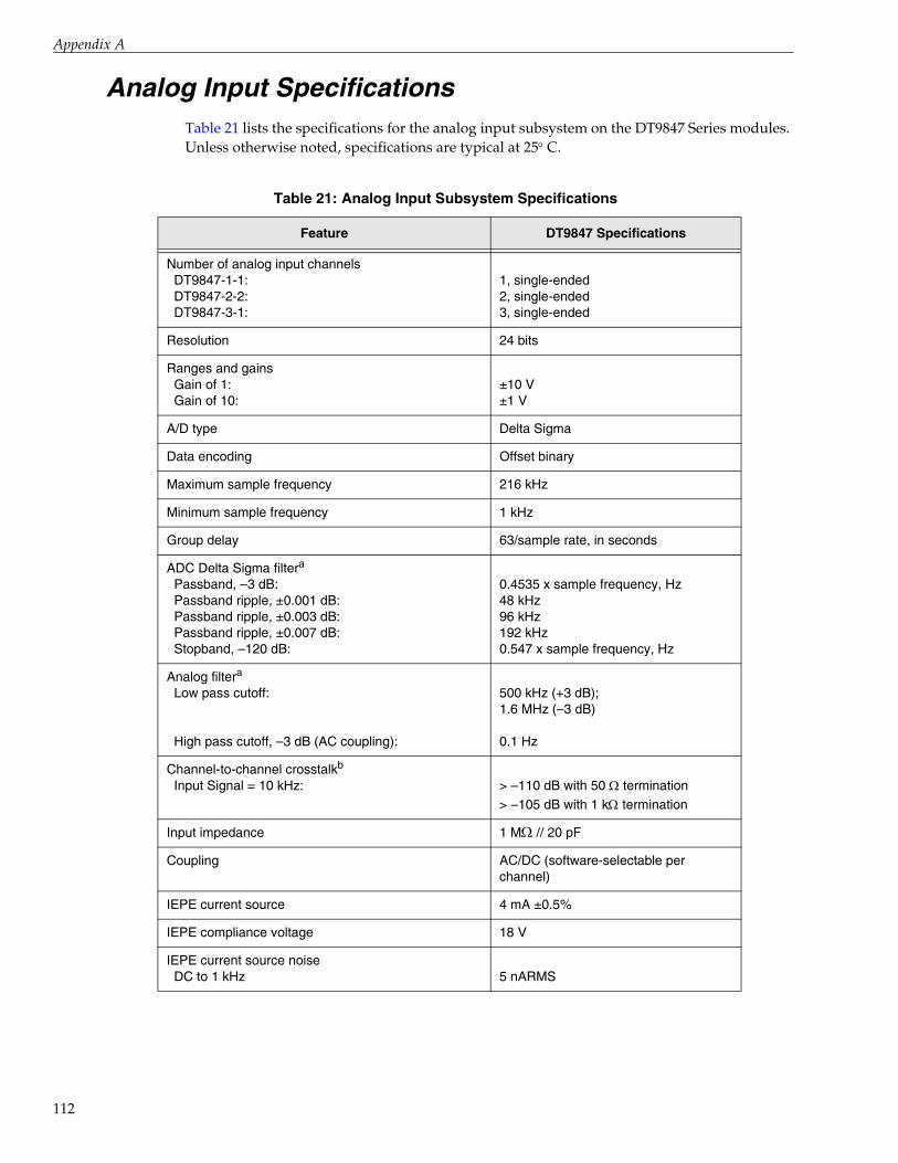
Appendix A
112
Analog Input SpecificationsTable 21 lists the specifications for the analog input subsystem on the DT9847 Series modules. Unless otherwise noted, specifications are typical at 25C.
Table 21: Analog Input Subsystem Specifications
Feature DT9847 Specifications
Number of analog input channelsDT9847-1-1:DT9847-2-2:DT9847-3-1:
1, single-ended2, single-ended3, single-ended
Resolution 24 bits
Ranges and gainsGain of 1:Gain of 10:
±10 V ±1 V
A/D type Delta Sigma
Data encoding Offset binary
Maximum sample frequency 216 kHz
Minimum sample frequency 1 kHz
Group delay 63/sample rate, in seconds
ADC Delta Sigma filtera
Passband, –3 dB:Passband ripple, ±0.001 dB:Passband ripple, ±0.003 dB:Passband ripple, ±0.007 dB:Stopband, –120 dB:
0.4535 x sample frequency, Hz 48 kHz96 kHz192 kHz0.547 x sample frequency, Hz
Analog filtera
Low pass cutoff:
High pass cutoff, –3 dB (AC coupling):
500 kHz (+3 dB); 1.6 MHz (–3 dB)
0.1 Hz
Channel-to-channel crosstalkb
Input Signal = 10 kHz: > –110 dB with 50 termination
> –105 dB with 1 k termination
Input impedance 1 M// 20 pF
Coupling AC/DC (software-selectable per channel)
IEPE current source 4 mA ±0.5%
IEPE compliance voltage 18 V
IEPE current source noiseDC to 1 kHz 5 nARMS
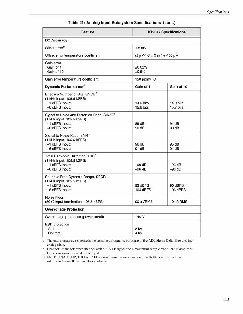
Specifications
DC Accuracy
Offset errorc 1.5 mV
Offset error temperature coefficient (2 V/C x Gain) + 400 V
Gain errorGain of 1:Gain of 10:
±0.02%±0.5%
Gain error temperature coefficient 150 ppm//C
Dynamic Performanced Gain of 1 Gain of 10
Effective Number of Bits, ENOBe
(1 kHz input, 105.5 kSPS)–1 dBFS input:–6 dBFS input:
14.6 bits15.6 bits
14.9 bits15.7 bits
Signal to Noise and Distortion Ratio, SINADf
(1 kHz input, 105.5 kSPS)–1 dBFS input:–6 dBFS input:
89 dB90 dB
91 dB90 dB
Signal to Noise Ratio, SNRg
(1 kHz input, 105.5 kSPS)–1 dBFS input:–6 dBFS input:
96 dB91 dB
95 dB91 dB
Total Harmonic Distortion, THDh
(1 kHz input, 105.5 kSPS)–1 dBFS input:–6 dBFS input:
–90 dB–96 dB
–93 dB–98 dB
Spurious Free Dynamic Range, SFDRi
(1 kHz input, 105.5 kSPS)–1 dBFS input:–6 dBFS input:
93 dBFS104 dBFS
96 dBFS106 dBFS
Noise Floor(50 input termination, 105.5 kSPS) 90 VRMS 10 VRMS
Overvoltage Protection
Overvoltage protection (power on/off) ±40 V
ESD protection Arc:Contact:
8 kV4 kV
a. The total frequency response is the combined frequency response of the ADC Sigma Delta filter and the analog filter.
b. Channel 0 is the reference channel with a 20 V PP signal and a maximum sample rate of 216 kSamples/s.c. Offset errors are referred to the input.d. ENOB, SINAD, SNR, THD, and SFDR measurements were made with a 16384 point FFT with a
minimum 4-term Blackman Harris window.
Table 21: Analog Input Subsystem Specifications (cont.)
Feature DT9847 Specifications
113
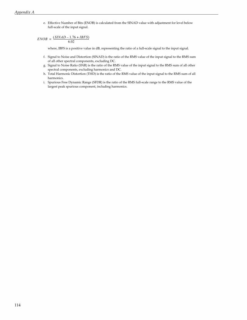
Appendix A
114
e. Effective Number of Bits (ENOB) is calculated from the SINAD value with adjustment for level below full-scale of the input signal.
where, IBFS is a positive value in dB, representing the ratio of a full-scale signal to the input signal.
f. Signal to Noise and Distortion (SINAD) is the ratio of the RMS value of the input signal to the RMS sum of all other spectral components, excluding DC.
g. Signal to Noise Ratio (SNR) is the ratio of the RMS value of the input signal to the RMS sum of all other spectral components, excluding harmonics and DC.
h. Total Harmonic Distortion (THD) is the ratio of the RMS value of the input signal to the RMS sum of all harmonics.
i. Spurious Free Dynamic Range (SFDR) is the ratio of the RMS full-scale range to the RMS value of the largest peak spurious component, including harmonics.
ENOB SINAD 1.76– IBFS+ 6.02
-----------------------------------------------------------=

Specifications
Figure shows the full system accuracy of the DT9847 Series module as measured by QuickDAQ. In this example, a 1 dB input signal is connected to the DT9847 Series module and is sampled at 216 kHz using a gain of 1. The effective number of bits (ENOB) is 14.62.
Figure 28: Dynamic Performance of the DT9847 Series Modules Measured Using QuickDAQ
115

Appendix A
116
Figure 29 shows the result of vector averaging data in QuickDAQ (FFT package). Vector averaging performs mathematical operations in the complex domain. This process cancels non-coherent noise components while allowing coherent signal components to remain.
In this example, a 10 dB input signal is connected to the DT9847 Series and is sampled at 50 kHz. You can clearly see the harmonics pulled out of the noise; the noise floor is below 150 dB.
Figure 29: Vector Averaging in QuickDAQ Allows Users to Isolate Coherent Signal Components

Specifications
Analog Output SpecificationsTable 22 lists the specifications for the analog output subsystem on the DT9847 Series modules. Unless otherwise noted, specifications are typical at 25C.
Table 22: Analog Output Subsystem Specifications
Feature DT9847 Series Specifications
Number of analog output channelsDT9847-1-1:DT9847-2-2:DT9847-3-1:
1, single-ended2, single-ended1, single-ended
Resolution 32 bits
D/A type Delta Sigma
Output range ±3 V or ±10 V, software programmablea
Data encoding Offset binary
Minimum sample frequency 30 kHz
Maximum sample frequency 216 kHz
Group delay (typical) 36/sample rate, in s
DAC Delta Sigma filterb
Passband, –3 dB: Passband ripple, ±0.005 dB:Stopband:Stopband attenuation, –100 dB:Stopband attenuation, –95 dB:Stopband attenuation, –90 dB:
0.49 x sample frequency, Hz0.454 x sample frequency, Hz0.546 x sample frequency, Hzsample frequency 44.1 kHzsample frequency 96 kHzsample frequency 192 kHz
Analog filterb 250 kHz, 2-pole, low-pass Butterworth
Output current ±3 mA maximum load (3 V across 1 k; 10 V across 3.3 k
Output FIFO 8 kSamples
Idle channel noise(216 kSPS)
±3 V range ±10 V range15 VRMS 30 VRMS
Total Harmonic Distortion, THDc
(216 kSPS–1 dBFS, 1 kHz output, 3.3 k load:–6 dBFS, 1 kHz output, 3.3 k load:
±3 V range ±10 V range–102 dB –106 dB–110 dB –110 dB
Spurious Free Dynamic Range, SFDRc
(216 kSPS)–1 dBFS, 1 kHz output, 3.3 k load:–6 dBFS, 1 kHz output, 3.3 k load:
±3 V range ±10 V range103 dB 108 dB107 dB 115 dB
Offset error ±1 mV
Offset error temperature coefficient ±3 V range ±10 V range100 V/C 130 V/C
Gain error ±1.0%
117

Appendix A
118
Gain error temperature coefficient ±3 V range ±10 V range30 ppm/C 55 ppm/C
Power fault and reset Goes to 0 V ±0.5 mV if the USB cable is removed, external power fails, USB power is reset, or the system is rebooted
ESD protection Arc:Contact:
8 kV4 kV
a. Older versions of this module may support only the ±3 V range.b. The total frequency response is the combined frequency response of the DAC Sigma Delta filter and the analog filter.c. THD and SFDR measurements were made with a 16384 point FFT with a minimum 4-term Blackman Harris window.
Table 22: Analog Output Subsystem Specifications (cont.)
Feature DT9847 Series Specifications

Specifications
Digital I/O SpecificationsTable 23 lists the specifications for the digital I/O subsystems on the DT9847 Series modules.
Table 23: Digital I/O Specifications
Feature Specifications
Number of digital I/O lines 8 (4 in, 4 out)
Number of ports 2 (4 bits each)
Logic family LVTTL (5 V tolerant)
Logic sense Positive true
InputsInput type: Input logic load: High input voltage: Low input voltage: Low input current:Termination:
Level-sensitive 1 LVTTL 2.0 V minimum 0.8 V maximum 0.4 mA maximum None
Outputs Fan out: High output:Low output: High output current: Low output current:
24 mA2.0 V minimum 0.8 V maximum –12 mA maximum12 mA maximum
Clocked with sample clock No
Software I/O selectable No
119

Appendix A
120
Trigger SpecificationsTable 24 lists the specifications for the trigger on the DT9847 Series modules.
Table 24: Trigger Specifications
Feature DT9847 Specifications
Trigger sourcesInternal software trigger: External digital trigger: Analog threshold trigger:
Software-initiated Software-selectableSoftware-selectable
External digital triggerInput type:
Logic family:Input logic load: Lower threshold:Upper threshold:Hysteresis:Input sink current:Minimum pulse width high/low:Maximum input signal:
Edge-sensitive, rising- or falling-edge trigger (software-selectable)LVTTL inputs1 LVTTL 1.1 V1.3 V0.2 V33 A1.3 s±30 V
Analog threshold triggerType:
Threshold level:Hysteresis:
Rising- or falling-edge threshold trigger on any analog input channel (software-selectable)10 V to +10 V @ gain of 1; ±1 V @ gain of 10100 mV
Trigger delay 1 conversion period maximum

Specifications
Master Oscillator SpecificationsTable 25 lists the specifications for the master oscillator on the DT9847 Series modules.
Table 25: Master Oscillator Specifications
Feature Specifications
Frequency 48 MHza
a. The sample frequencies for the A/D and D/A subsystems are independently programmable and are derived from the same 48 MHz reference clock. Therefore, it is possible to establish a fixed relationship betwen the A/D and D/A subsystem sample frequencies, including setting them to the same frequency (30 kHz to 216 kHz). However, the subsystems are not designed to be synchronous with each other.
Accuracy at 25 C ±30 ppm
Drift over temperature 0 to 70C (Total) ±50 ppm
Aging (first year) ±5 ppm
Maximum error (first year) ±85 ppm
121

Appendix A
122
Power, Physical, and Environmental SpecificationsTable 26 lists the power, physical, and environmental specifications for the DT9847 Series modules.
.Table 26: Power, Physical, and Environmental Specifications
FeatureDT9847 SeriesSpecifications
PowerDT9847-1-1 and DT9847-1-1-OEM:
DT9847-2-2, DT9847-2-2-OEM, DT9847-3-1, and DT9847-3-1-OEM:
5 V ±0.30 V@ 600 mAa
+5 V to 24 V @ 5 Wb
a. The DT9847-1-1 requires a USB-Y cable (EP399) to ensure that adequate power is provided. Refer to page 33 for more information on connecting the USB-Y cable. The DT9847-1-1-OEM can be powered with USB power using the EP399 USB-Y cable or by using an external power supply connected to screw terminal block TB1 (this requires a jumper); refer to page 134 for more information.
b. To power the DT9847-2-2 and DT9847-3-1, connect the EP394 external power supply to the barrel power connector on the module. To power the DT9847-2-2 OEM and DT9847-3-1-OEM modules, connect the EP394 external power supply either to the barrel power connector on the module or to screw terminal block TB1 on the module, as described on page 136.
Warm-up time 1 hour
Physical Dimensions - EnclosureLength:Width:Height:Weight:
10.025 inches (254.63 mm)4.170 inches (105.92 mm)1.575 inches (40 mm)22.62 ounces (641.5 g)
Physical Dimensions - OEM (board only)Length:Width:Height:Weight:
10.025 inches (254.63 mm)3.937 inches (100 mm)0.712 inches (18.08 mm)6.5 ounces (184.2 g)
Environmental Operating temperature range: Storage temperature range: Relative humidity:
Altitude:
0C to55C–25C to 85CTo 95%, noncondensingTo 10,000 feet

Specifications
Regulatory SpecificationsThe DT9847 Series is CE-compliant. Table 27 lists the regulatory specifications for the DT9847 Series modules.
Table 27: Regulatory Specifications
Feature DT9847 Series Specifications
Emissions (EMI) FCC Part 15, Class AEN55011:2007 (Based on CISPR-11, 2003/A2, 2006)
Immunity EN61326-1:2006 Electrical Equipment for Measurement, Control, and Laboratory Use
EMC RequirementsEN61000-4-2:2009Electrostatic Discharge (ESD) 4 kV contact discharge,8 kV air discharge, 4 kV horizontal and vertical coupling planes
EN61000-4-3:2006Radiated electromagnetic fields, 3 V/m, 80 to 1000 MHz; 3 V/m, 1.4 GHz to 2 GHz; 1 V/m, 2 GHz to 2.7 GHz
EN61000-4-4:2004Electrical Fast Transient/Burst (EFT) 1 kV on data cables
EN61000-4-6:2009Conducted immunity requirements, 3 Vrms on data cables150 kHz to 80 MHz
RoHS (EU Directive 2002/95/EG) Compliant (as of July 1st, 2006)
123

Appendix A
124
Connector SpecificationsTable 28 lists the connector specifications for the DT9847 Series modules.
Table 28: Connector Specifications
Feature Specifications
Analog I/O BNC connectors TE Connectivity 5227161-9
External power supply Jack on the module: Switchcraft #L722RAMating plug assembly, 0.08 inch: Switchcraft #S761K
Sync Bus connector (RJ45) Molex part number 44661-0001
USB connector TE Connectivity 292304-2
Digital I/O connector Kycon K66X-E15S-N

Specifications
External Power Supply SpecificationsTable 29 lists the specifications for the EP394 +5 V external power supply that is used with the DT9847 Series modules.
Table 29: External Power Supply (EP394) Specifications
Feature Specifications
Type FRIWO medical power supply (GPP 10)
Input voltage 100 to 240 V AC (±10%)
Input current 250 mA
Frequency 50 to 60 Hz
Efficiency 80% typical at full load
Output voltage 5 V
Output current 1600 mA
Output ripple voltage 75 mVpp
Regulatory standards UL, VDE, CE, Energy Star compliant
125

Appendix A
126
BConnector Pin Assignments and LED
Status IndicatorsDigital I/O and External Trigger Connector . . . . . . . . . . . . . . . . . . . . . . . . . . . . . . . . . . . . . 128
External USB Connector . . . . . . . . . . . . . . . . . . . . . . . . . . . . . . . . . . . . . . . . . . . . . . . . . . . . . . 129
External Power Connector . . . . . . . . . . . . . . . . . . . . . . . . . . . . . . . . . . . . . . . . . . . . . . . . . . . . 130
STP15 Screw Terminal Panel . . . . . . . . . . . . . . . . . . . . . . . . . . . . . . . . . . . . . . . . . . . . . . . . . . 131
LED Status Indicators . . . . . . . . . . . . . . . . . . . . . . . . . . . . . . . . . . . . . . . . . . . . . . . . . . . . . . . . 132
127
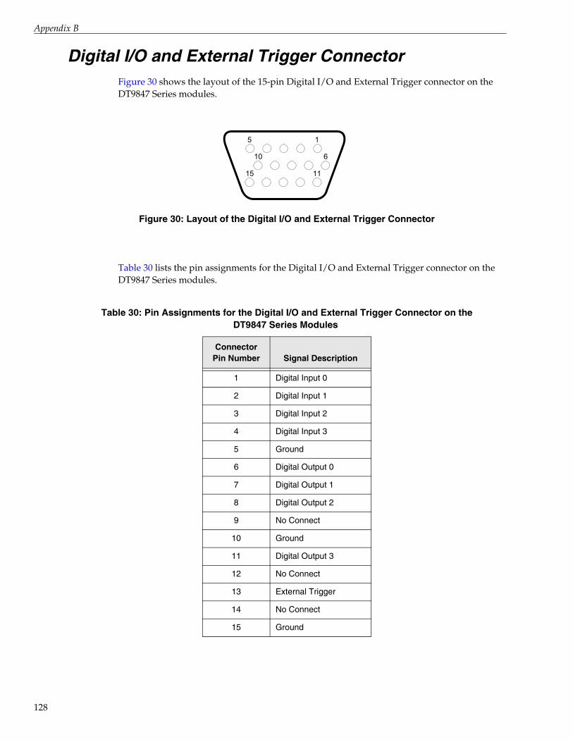
Appendix B
128
Digital I/O and External Trigger ConnectorFigure 30 shows the layout of the 15-pin Digital I/O and External Trigger connector on the DT9847 Series modules.
Figure 30: Layout of the Digital I/O and External Trigger Connector
Table 30 lists the pin assignments for the Digital I/O and External Trigger connector on the DT9847 Series modules.
Table 30: Pin Assignments for the Digital I/O and External Trigger Connector on the DT9847 Series Modules
Connector Pin Number Signal Description
1 Digital Input 0
2 Digital Input 1
3 Digital Input 2
4 Digital Input 3
5 Ground
6 Digital Output 0
7 Digital Output 1
8 Digital Output 2
9 No Connect
10 Ground
11 Digital Output 3
12 No Connect
13 External Trigger
14 No Connect
15 Ground
15
1115
610

Connector Pin Assignments and LED Status Indicators
External USB ConnectorFigure 31 shows the layout of the external USB connector on the DT9847 Series modules.
Figure 31: Layout of the USB Connector
Table 31 lists the pin assignments for the USB connector on the DT9847 Series modules.
Table 31: Pin Assignments for the USB Connector on the DT9847 Series Modules
Connector Pin Number Signal Description
Connector Pin Number Signal Description
1 USB +5 V 3 USB Data +
2 USB Data – 4 USB Ground
1
2 3
4
129
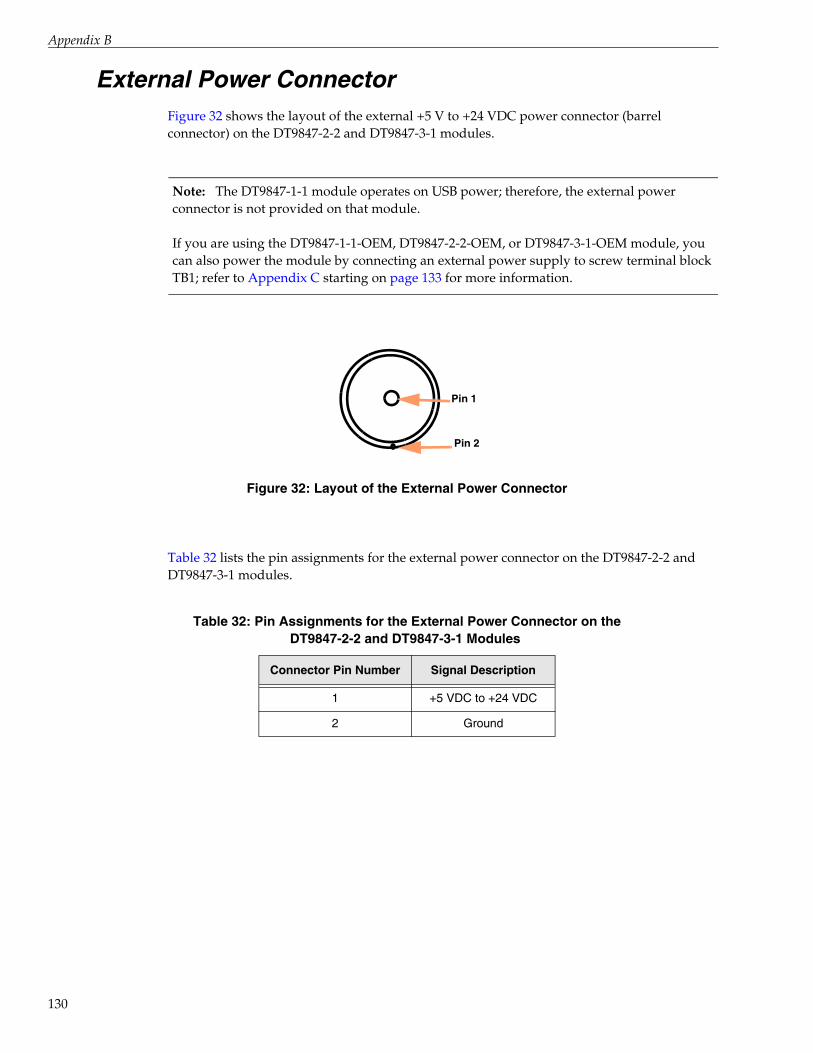
Appendix B
130
External Power ConnectorFigure 32 shows the layout of the external +5 V to +24 VDC power connector (barrel connector) on the DT9847-2-2 and DT9847-3-1 modules.
Note: The DT9847-1-1 module operates on USB power; therefore, the external power connector is not provided on that module.
If you are using the DT9847-1-1-OEM, DT9847-2-2-OEM, or DT9847-3-1-OEM module, you can also power the module by connecting an external power supply to screw terminal block TB1; refer to Appendix C starting on page 133 for more information.
Figure 32: Layout of the External Power Connector
Table 32 lists the pin assignments for the external power connector on the DT9847-2-2 and DT9847-3-1 modules.
Table 32: Pin Assignments for the External Power Connector on theDT9847-2-2 and DT9847-3-1 Modules
Connector Pin Number Signal Description
1 +5 VDC to +24 VDC
2 Ground
Pin 1
Pin 2

Connector Pin Assignments and LED Status Indicators
STP15 Screw Terminal PanelThe STP15 contains one 15-pin connector and two screw terminal blocks (TB1 and TB2). The 15-pin connector provides access to the signals from the Digital I/O and External Trigger connector on the DT9847 module.
Figure 33 shows the layout of the STP15 and lists the screw terminal assignments.
Figure 33: Layout of the STP15 Screw Terminal Panel
Note: The dark filled circles in Figure 33 represent holes that you can use to mount the STP15 on a DIN rail. To mount the STP15 on a DIN rail, you need two DIN rail mount adapters (Phoenix Contact part number 1201578), and four thread form screws (Bossard part number BN2724M3x8).
IN0
TB1
IN1
DGND
IN2
IN3
DGND
STROBE*
DGND/TRIGGER
DGND
TB2
+5 V*
DGND
OUT3
OUT2
DGND
OUT1
OUT0
J1, 15-Pin Connector
*These signal are not used on the DT9847 Series modules.
131
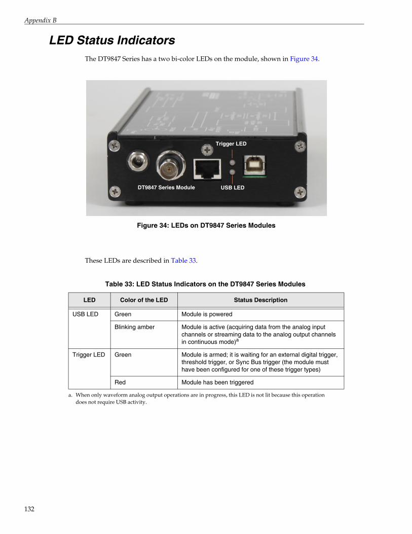
Appendix B
132
LED Status IndicatorsThe DT9847 Series has a two bi-color LEDs on the module, shown in Figure 34.
Figure 34: LEDs on DT9847 Series Modules
These LEDs are described in Table 33.
Table 33: LED Status Indicators on the DT9847 Series Modules
LED Color of the LED Status Description
USB LED Green Module is powered
Blinking amber Module is active (acquiring data from the analog input channels or streaming data to the analog output channels in continuous mode)a
a. When only waveform analog output operations are in progress, this LED is not lit because this operation does not require USB activity.
Trigger LED Green Module is armed; it is waiting for an external digital trigger, threshold trigger, or Sync Bus trigger (the module must have been configured for one of these trigger types)
Red Module has been triggered
Trigger LED
USB LEDDT9847 Series Module

CPowering OEM Modules
Powering the DT9847-1-1-OEM Module . . . . . . . . . . . . . . . . . . . . . . . . . . . . . . . . . . . . . . . . 134
Powering the DT9847-2-2-OEM or DT9847-3-1-OEM Module . . . . . . . . . . . . . . . . . . . . . . 136
133
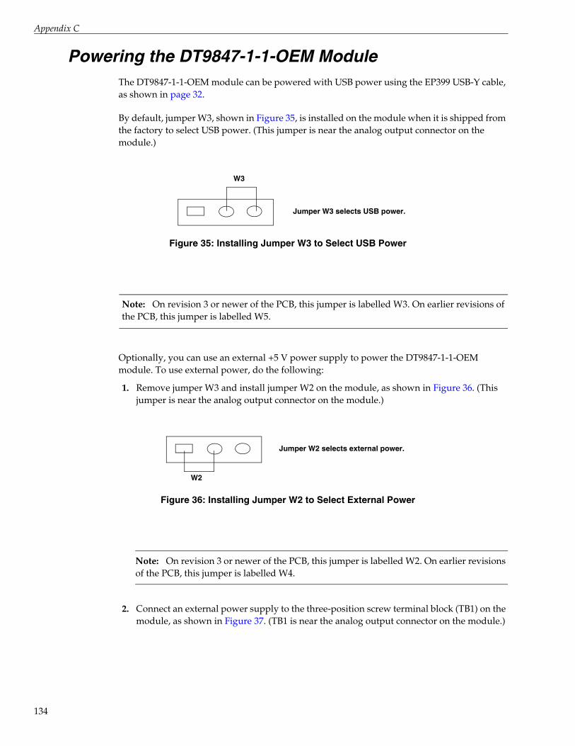
Appendix C
134
Powering the DT9847-1-1-OEM ModuleThe DT9847-1-1-OEM module can be powered with USB power using the EP399 USB-Y cable, as shown in page 32.
By default, jumper W3, shown in Figure 35, is installed on the module when it is shipped from the factory to select USB power. (This jumper is near the analog output connector on the module.)
Figure 35: Installing Jumper W3 to Select USB Power
Note: On revision 3 or newer of the PCB, this jumper is labelled W3. On earlier revisions of the PCB, this jumper is labelled W5.
Optionally, you can use an external +5 V power supply to power the DT9847-1-1-OEM module. To use external power, do the following:
1. Remove jumper W3 and install jumper W2 on the module, as shown in Figure 36. (This jumper is near the analog output connector on the module.)
Figure 36: Installing Jumper W2 to Select External Power
Note: On revision 3 or newer of the PCB, this jumper is labelled W2. On earlier revisions of the PCB, this jumper is labelled W4.
2. Connect an external power supply to the three-position screw terminal block (TB1) on the module, as shown in Figure 37. (TB1 is near the analog output connector on the module.)
W3
Jumper W3 selects USB power.
W2
Jumper W2 selects external power.

Powering OEM Modules
Figure 37: Connecting an External Power Supply to Screw Terminal TB1 on the Module
+5 V
TB1
1
2
3
Groun
Shield (Chassis Ground)
On the DT9847-1-1-OEM, ensure that the maximum voltage of the external supply is +5 V ±0.30 V @ 600 mA. Higher voltages will destroy the module.
135

Appendix C
136
Powering the DT9847-2-2-OEM or DT9847-3-1-OEM Module
The DT9847-2-2-OEM or DT9847-3-1-OEM module must be externally powered with a +5 V to 24 V @ 5 W power supply.
You can connect an external power supply either to the barrel power connector on the module, as shown on page 31, or to the three-position screw terminal block (TB1) on the module, as shown in Figure 38.
Figure 38: Connecting an External Power Supply to Screw Terminal TB1 on the Module
TB1
1
2
3
The DT9847-2-2-OEM and DT9847-3-1-OEM modules accept an +5 V to 24 V @ 5 W external power supply.
+5 V to 24 V
Groun
Shield (Chassis Ground)

DRegister-Level Programming
Writing to the EEPROM Register. . . . . . . . . . . . . . . . . . . . . . . . . . . . . . . . . . . . . . . . . . . . . . . 138
137

Appendix D
138
Writing to the EEPROM RegisterIf you want to change the default values that are defined in the Open Layers Control Panel programmatically, you can use the Data Acq SDK function olDiagWriteReg to write to the EEPROM register of the module.
On the DT9847 Series modules, the Open Layers Control Panel has controls for setting the following parameters, which are stored in 8 consecutive bytes of EEPROM:
• Channel 0, 1, and 2 coupling type. The values AC or DC are stored as constants for these controls.
• Channel 0, 1 and 2 current source. The values INTERNAL, EXTERNAL or DISABLED are stored as constants for these controls. Note that while the control panel has only two states (Enabled and Disabled), three states are actually defined, as follows:
INTERNAL = Enabled (used by the control panel)
EXTERNAL = Disabled
DISABLED = Disabled (used by the control panel)
These controls may also be “uninitialized” if for some reason, the module skipped the post-manufacturing initialization process.
To access the storage locations programmatically, use the olDiagReadReg() and olDiagWriteReg() functions. The following code shows the location of these controls in the register map:
#define EEPROM_MEM_BASE 0x100000// Coupling storage offsets relative to the base address for the// three analog input channelsconst EEPROM_OFFSET_COUPLING_0 = 0x0020;const EEPROM_OFFSET_COUPLING_1 = 0x0021;const EEPROM_OFFSET_COUPLING_2 = 0x0022;// Current source storage offsets relative to the base address for// the three analog input channelsconst EEPROM_OFFSET_CURRENT_SOURCE_0 = 0x0024;const EEPROM_OFFSET_CURRENT_SOURCE_1 = 0x0025;const EEPROM_OFFSET_CURRENT_SOURCE_2 = 0x0026;
Note: olDiagReadReg() and olDiagWriteReg() require a ULONG value for the data parameter, but we are reading and writing only a single byte (last parameter).

Register-Level Programming
// For example, to read the current source power-up default for // channel 2,use the following code:ULONG Channel_2_Current_Source;OLSTATUS olStatus = olDiagReadReg(m_hDev, EEPROM_MEM_BASE +
EEPROM_OFFSET_CURRENT_SOURCE_2, &Channel_2_Current_Source, 1);
// For example, to set the coupling power-up default for channel 0 // to AC, use the following code:OLSTATUS olStatus = olDiagWriteReg(m_hDev, EEPROM_MEM_BASE +
EEPROM_OFFSET_COUPLING_0, (ULONG) AC, 1);
139

Appendix D
140

Index
Index
AAC coupling 92accessories 79, 80
BNC DIN Rail Kit 22EP337 cable 21EP386 panel 22STP15 screw terminal panel 21
administrator privileges 36aliasing 65analog input
calibrating 108channels 64conversion modes 66data format and transfer 71error conditions 71gain 64IEPE functions 65input range 64resolution 65sample clock 65single-ended configuration 40single-value operations 66single-values operations 67specifications 112triggers 69wiring 40
analog outputcalibrating 110channels 72clock sources 72continuous operations 74conversion modes 73data format and transfer 76error conditions 76gain 72ranges 72resolution 72single-value operations 73specifications 117waveform generation mode 73wiring 41
analog threshold trigger 69, 70, 76applet, Open Layers Control Panel 101application wiring
analog inputs 40analog output 41
digital inputs and outputs 43
Bbase clock frequency 95BaseClockFrequency 95binary data encoding 88BNC DIN Rail Kit 22buffers 88
inprocess flush 88single wrap mode 88
CC/C++ programs 20cables, USB 32, 34calibrating the module
analog input subsystem 108analog output subsystem 110running the calibration utility 107
CGLDepth 89channel type
single-ended 89channel-gain list depth 89channels
analog input 64analog output 72digital I/O 77number of 89
clocksanalog input 65analog output 72base frequency 95internal 95maximum external clock divider 95maximum throughput 95minimum external clock divider 95minimum throughput 95simultaneous 95
connecting signalsanalog inputs 40analog output 41digital inputs and outputs 43
connecting to the host computer 32connector J1 pin assignments 132connectors
external +5 V 130
141

Index
142
external USB 129continuous analog input
post-trigger 87continuous analog output 87continuous counter/timer 87continuous digital I/O 87Control Panel applet 101conversion modes
continuous analog output 74digital I/O 77single-value analog input 66single-value analog output 73single-values analog input 67waveform generation mode 73
conversion rate 67counter/timer
channels 89clock sources 95
coupling type 65current source 65, 92customer service 103
DDAQ Adaptor for MATLAB 20data encoding 71, 76, 88data flow modes
continuous C/T 87continuous digital input 87continuous post-trigger 87single-value 87waveform stored in FIFO only 87
data format and transferanalog input 71analog output 76
DataAcq SDK 20DC coupling 92device driver 18device drivers 36Device Selection window 49digital I/O 77
lines 77operation modes 77single-value operations 77subsystem specifications 119wiring 43
digital trigger 69, 70, 75DT9847 Series Calibration Utility 18DT-Open Layers for .NET Class Library 20
EEEPROM register 138encoding data 71, 76environmental specifications 122EP337 cable 21EP386 panel 22, 79, 80errors
analog input 71analog output 76
excitation current source 65available 92internal 92
expansion hub 34external +5 V connector 130external clock divider
maximum 95minimum 95
external digital trigger 69, 70, 75negative TTL 93, 94positive TTL 93, 94
external USB connector 129
Ffactory service 103features 14FIFO
input 71output 74
FifoSize 87formatting data
analog input 71analog output 76
frequencyanalog input operations 65, 73base clock 95internal A/D clock 95internal A/D sample clock 95internal C/T clock 95internal retrigger clock 88
Ggain 64
actual available 89analog output 72number of 89programmable 89
group delay 66, 73

Index
Hhardware features 14hot-swapping 32
IIEPE features 65IEPE support 92inprocess buffers 88input
channels 64configuration, single-ended 40ranges 64resolution 65
input FIFO 71internal clock 95internal excitation current source 92interrupts 87
JJ1 connector pin assignments 132J5 connector 130J6 connector 129jumper
W2 134W3 134
LLabVIEW 20LED 32, 34LED status indicator 132LEDs 132legacy CPL elevated 36lines, digital I/O 77LV-Link 20
Mmaster device 50master oscillator, specifications 121MATLAB 20MaxExtClockDivider 95MaxFrequency 95MaxMultiScanCount 88MaxRetriggerFreq 88MaxSingleEndedChannels 89MinExtClockDivider 95MinFrequency 95MinRetriggerFreq 88
multiple modules, triggering 78muting the output voltage 87
Nnegative threshold trigger 93, 94number of
gains 89I/O channels 89resolutions 90scans per trigger 88single-ended channels 89voltage ranges 90
NumberOfChannels 89NumberOfRanges 90NumberOfResolutions 90NumberOfSupportedGains 89Nyquist Theorem 65
OolDiagReadReg 138olDiagWriteReg 138Open Layers Control panel 36Open Layers Control Panel applet 101operation modes
single-value analog input 66single-value analog output 73single-value digital I/O 77single-values analog input 67waveform generation 73
oscillator, specifications 121output
clock sources 72ranges 72
output FIFO 74
Pphysical specifications 122pin assignments 132ports, digital I/O 77positive threshold trigger 93, 94post-trigger acquisition mode 87post-trigger scan count 94power 14, 31, 34, 35
specifications 122power supply 31powering OEM modules
DT9847-1-1-OEM 134DT9847-2-2-OEM or DT9847-3-1-OEM 136
143

Index
144
preparing to wire signals 39
QQuick DataAcq application 20QuickDAQ 48
Advanced FFT Analysis option 19Base version 18FFT Analysis option 19
Rranges
analog input 64analog output 72number of 90
recommendations for wiring 39reference trigger 70
analog threshold trigger 70external digital trigger 70Sync Bus 70
register-level programming 138regulatory specifications 123resolution
analog input 65analog output 72available 90number of 90
retrigger clock frequency 88returning boards to the factory 103RMA 103
Ssample clock 65scan count 94screw terminal block, TB1 135, 136screw terminal panel layout 44, 131SDK 20simultaneous clocking 95simultaneous sample-and-hold support 89simultaneous start list 87single buffer wrap mode 88single-ended channels 40, 89
number of 89single-value configuration 66single-value operations 87
analog output 73digital I/O 77
single-values configuration 67size, module 122
software trigger 69, 75, 93specifications 111, 133
analog input 112analog output 117connector 124digital I/O 119environmental 122external power supply 125master oscillator 121physical 122power 122regulatory 123triggers 120
start triggeranalog threshold trigger 69external digital (TTL) trigger 69, 70software 69
start trigger sources 69stopping an operation 67, 75STP15 screw terminal panel 21, 43, 131
layout 44SupportedExcitationCurrentValues 92SupportedGains 89SupportedResolutions 90SupportedThresholdTriggerChannel 93, 94SupportedVoltageRanges 90SupportsACCoupling 92SupportsBinaryEncoding 88SupportsBuffering 88SupportsContinuous 87SupportsDCCoupling 92SupportsIEPE 92SupportsInProcessFlush 88SupportsInternalClock 95SupportsInternalExcitationCurrentSrc 92SupportsMute 87SupportsNegExternalTTLTrigger 93, 94SupportsNegThresholdTrigger 93, 94SupportsPosExternalTTLTrigger 93, 94SupportsPosThresholdTrigger 93, 94SupportsPostTriggerScanCount 94SupportsProgrammableGain 89SupportsSimultaneousClocking 95SupportsSimultaneousSampleHold 89SupportsSimultaneousStart 87SupportsSingleEnded 89SupportsSingleValue 87SupportsSoftwareTrigger 93SupportsSynchronization 87SupportsWaveformModeOnly 87SupportsWrapSingle 88

Index
Sync Bus trigger 70synchronization modes 87SynchronizationMode 87system requirements 30
TTB1 screw terminal block 135, 136technical support 102threshold trigger 76
channel 93, 94negative 93, 94
threshold trigger, positive 93, 94throughput
maximum 95minimum 95
trademark and copyright information 2transferring data
analog input 71analog output 76
Trigger LED 33, 68, 132triggered scan
number of scans per trigger 88retrigger frequency 88
triggering acquisition on multiple modules 78triggers
analog input 69analog threshold 69, 76external 69, 70, 75external negative digital 93, 94external positive digital 93, 94negative threshold 93, 94positive threshold 93, 94software 69, 75, 93specifications 120
troubleshootingprocedure 100technical support 102troubleshooting table 100
TTL trigger 69, 70, 75
Uunmuting the output voltage 87unpacking 29USB cable 32, 34USB expansion hub 34USB LED 33, 34, 68, 132
VVisual Basic for .NET programs 20Visual C# programs 20voltage ranges 64, 90
number of 90
WW2 jumper 134W3 jumper 134warm-up time 39, 108wiring signals 39
analog inputs 40analog output 41digital inputs and outputs 43preparing 39recommendations 39
writing programs inC/C++ 20Visual Basic .NET 20Visual C# 20
145

Index
146


