RELEASED PM3386 DATASHEET PMC-1991129 ISSUE 7 DUAL GIGABIT ETHERNET CONTROLLER PROPRIETARY AND CONFIDENTIAL TO PMC-SIERRA, INC., AND FOR ITS CUSTOMERS’ INTERNAL USE PM3386 S/UNI-2xGE DUAL GIGABIT ETHERNET CONTROLLER DATASHEET PROPRIETARY AND CONFIDENTIAL RELEASED ISSUE 7: JULY 2001
PROPRIETARY AND CONFIDENTIAL TO PMC-SIERRA, INC., AND FOR ITS CUSTOMERS’ INTERNAL USE
REVISION HISTORY
IssueNo.
Issue Date Originator Details of Change
7 July 2001 KarenLeandro
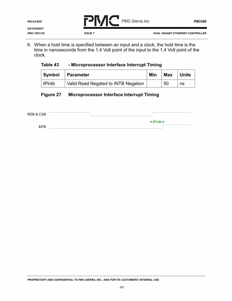
Release to Production DatasheetUpdated DC Characteristics with qualifiedvaluesAdded SERDES ModeAdded GMII/TBI ModeModified timing contained within SERDESTransmit Data TimingModified timing contained within SERDESReceived Data Timing
PROPRIETARY AND CONFIDENTIAL TO PMC-SIERRA, INC., AND FOR ITS CUSTOMERS’ INTERNAL USE
1
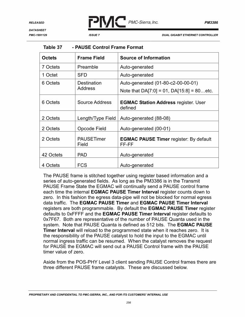
1 DEFINITIONSCSMA/CD Carrier Sense Multiple Access with Collision Detection.1000BASE-T IEEE 802.3-1998 Physical Layer specification for 1000 Mb/s
CSMA/CD LAN using four pairs of Category 5 balanced coppercabling.
1000BASE-SX IEEE 802.3-1998 using short wavelength laser devices overmultimode fiber
1000BASE-LX IEEE 802.3-1998 using long wavelength laser devices overmultimode and single-mode fiber.
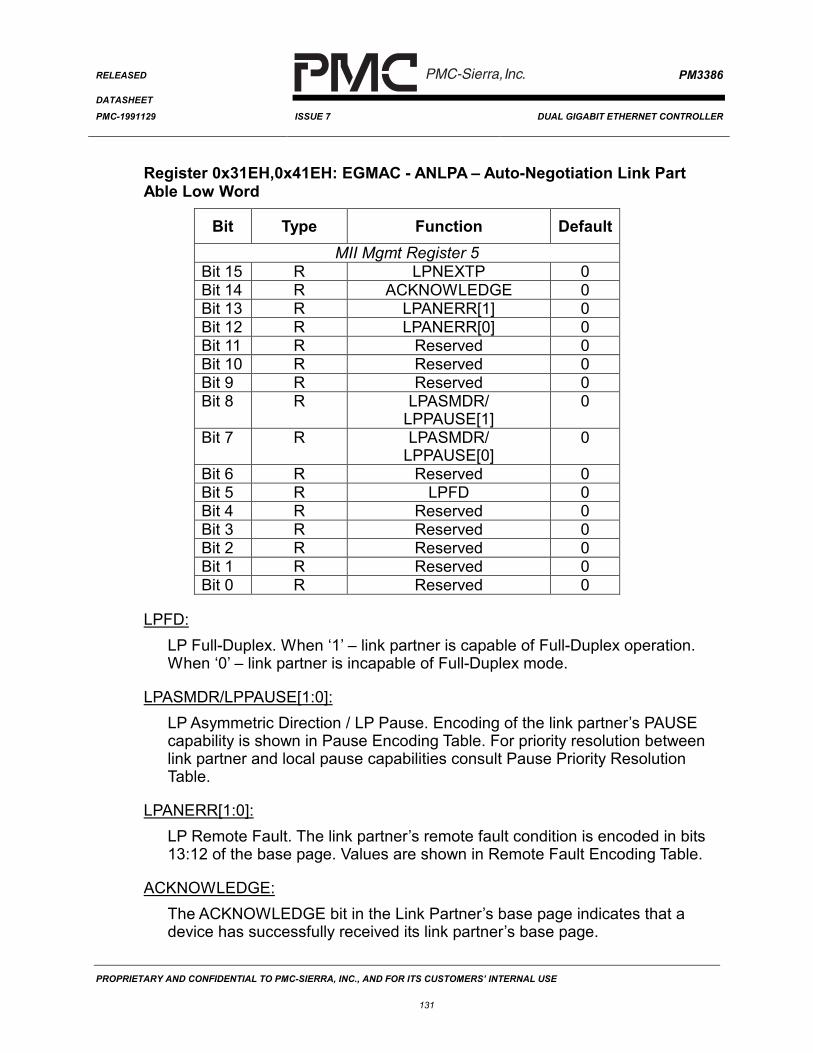
Auto-Negotiation The algorithm that allows two devices at either end of a linksegment to negotiate common data service functions.
Base Page The first 16-bit message exchanged during IEEE 802.3-1998Auto-Negotiation.
Comma The seven-bit sequence that is part of an 8B/10B code-groupthat is used for the purpose of code-group alignment.
Comma- The seven-bit sequence (1100000) of an encoded datastream.
Comma+ The seven-bit sequence (0011111) of an encoded data stream.Data Frame Consists of Destination Address, Source Address, Length
Field, logical link control (LLC) Data, PAD, and Frame CheckSequence.
DTE Any source or destination of data connected to the local areanetwork.
EOF End of frame.EOP End of packetEven Parity The count of the number of 1’s in the data word of n bits. If
there are an odd number of 1s, then the parity bit will be a 1 sothat including the parity bit, the number of 1s are an evennumber.
Frame Same as Data FrameFull Duplex A mode of operation that supports simultaneous
communication between a pair of stations, provided that thePhysical Layer is capable of supporting simultaneoustransmission and reception without interference.
GMII Gigabit Media Independent Interface.IPG Inter-Packet Gap (IPG): A delay or time gap between
CSMA/CD physical packets intended to provided interframerecovery time for other CSMA/CD sublayers and for thePhysical Medium.
MIB Management Information Base (MIB): A repository ofinformation to describe the operation of specific networkdevice.
PROPRIETARY AND CONFIDENTIAL TO PMC-SIERRA, INC., AND FOR ITS CUSTOMERS’ INTERNAL USE
2
MAC Media Access Control (MAC): The data link sublayer that isresponsible for transferring data to and from the PhysicalLayer.
MII Media independent Interface (MII): A transparent signalinterface at the bottom of the Reconciliation sublayer.
Next Page General class of pages optionally transmitted by Auto-Negotiation able devices following the base page wordnegotiation.
Nibble A group of four data bits. The unit of exchange on the MII.Packet The logical unit of data transferred across the POS-PHY Level
3 interface. This generally corresponds to the Data Frame asdefined previously, although the CRC may or may not bepresent in the POS-PHY Level 3 egress direction.
Physical Packet Consists of a Data Frame as defined previously, preceded bythe Preamble and the Start Frame Delimiter, encoded, asappropriate, for the Physical Layer (PHY) type.
POS-PHY SATURN compatible Packet over SONET interfacespecification for physical layer devices. POS-PHY level 3defines an interface for bit rates up to and including 2.488Gbit/s.
PL3 Short hand notation for the POS-PHY Level 3 term.Odd Parity The count of the number of 1’s in the data word of n bits. If
there are an odd number of 1s, then the parity bit will be a 0 sothat including the parity bit, the number of 1s are an oddnumber
PROPRIETARY AND CONFIDENTIAL TO PMC-SIERRA, INC., AND FOR ITS CUSTOMERS’ INTERNAL USE
3
2 FEATURES
2.1 General
• Two port full-duplex Gigabit Ethernet Controller with an industry standard POS-PHYLevel 3 system interface.
• Provides direct connect to optics via two internal Serializer/Deserializer (SERDES)• Provides connection to copper Gigabit Ethernet physical layer devices via two GMII
specification.• Provides on-chip data recovery and clock synthesis.• Supports dual IEEE 802.3 -1998 GMII interfaces for connection to copper Gigabit
Ethernet physical layer devices.• Provides dual standard IEEE 802.3 Gigabit Ethernet MACs for frame verification.• Enables frame filtering on 8 unicast or 64 multicast entries.• Internal 16k byte egress and 64k byte ingress FIFOs per channel to accommodate
system latencies.• Incorporates SATURN POS-PHY Level 3 32-bit System Interface clocked up to
104 MHz (32 bit mode only).• Line side loopback capability for system level diagnostic capability.• Includes 16 bit generic microprocessor interface for device initialization, control,
register and per port statistics access.• Provides a standard 5 signal P1149.1 JTAG test port for boundary scan board test
purposes.• Low power 1.8V CMOS device with 3.3V TTL compatible digital inputs (5V TTL
compatible microprocessor inputs) and 3.3V CMOS/TTL compatible digital outputswithin a 352 pin 27mm by 27mm UBGA package.
• Industrial temperature range (-40°C to +85°C).
2.2 Line Side Interface
• SERDES interface provides 2 differential pairs at 1250 MHz for connection toelectrical optical modules.
• GMII interface provides 8 bit wide TX & RX data interfaces at 125 MHz with controlsignals for connection to copper Gigabit Ethernet physical layer devices.
• Allows selection between SERDES and GMII interface on a per channel basis.
PROPRIETARY AND CONFIDENTIAL TO PMC-SIERRA, INC., AND FOR ITS CUSTOMERS’ INTERNAL USE
4
2.3 Gigabit Ethernet MAC
• Verifies frame integrity (i.e. FCS and length checks).• Erred frames can be filtered or passed to higher layer device.• Automatic Base page Auto-Negotiation, extended Auto-Negotiation (Next Page)
supported via host.• Egress Ethernet physical frame encapsulation (pad to min size, add preamble, IFG
and CRC generation).• Supports Ethernet 2.0, IEEE 802.3 LLC and IEEE 802.3 SNAP/LLC encoding
formats and VLAN tagged frames.• Provides 8 unicast exact-match address filters to filter frames based on DA or SA
with optional VID.• Each address filter can be programmed to indicate whether to accept or discard
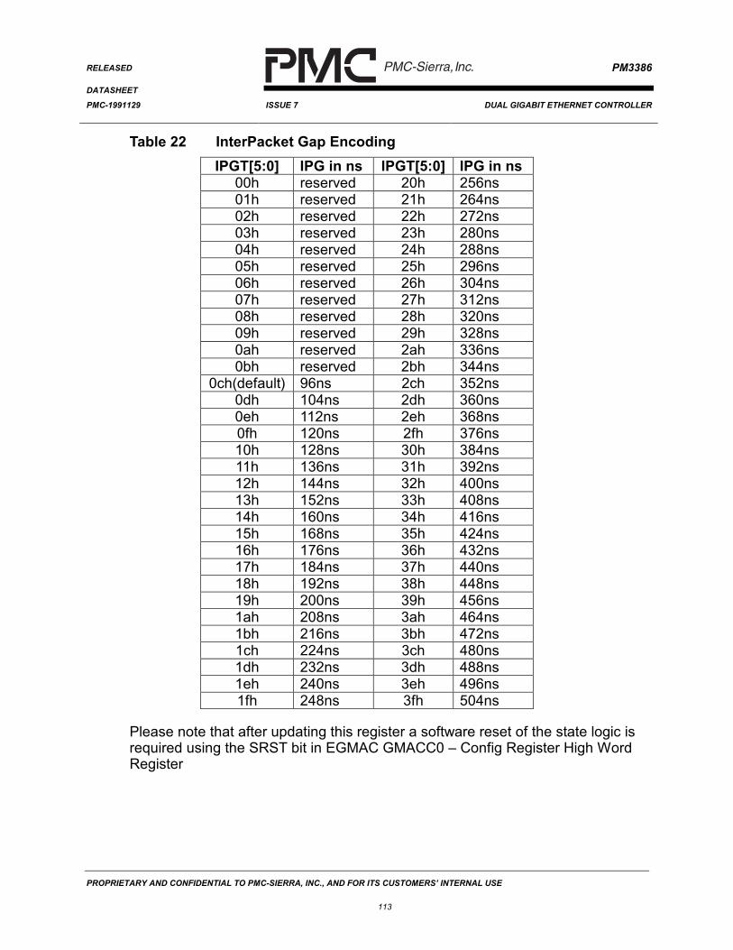
based on a match.• Provides a 64 group multicast address filter.• Supports 64 byte minimum size frames and jumbo frames up to 9.6K bytes.• Programmable Inter-packet gap (IPG).• System side loopback through GMAC for diagnostic capability.
2.4 Flow Control
• Supports IEEE 802.3-1998 flow control at each Ethernet port if enabled.• Programmable watermarks for full/empty FIFO thresholds.• Automatic generation of PAUSE frames based on FIFO fill levels.• Upper layer device can flow control Ethernet ports using side-band or host signaling
to cause generation of a PAUSE frame.• Provides side-band Paused state indication to upstream devices.• Loss-less flow control on all valid frames up to 9.6k bytes.
2.5 Statistics
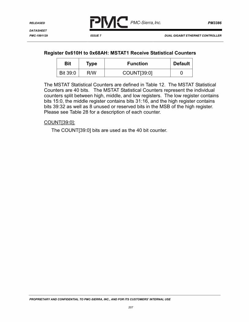
• 40 bit counters are used to ensure rollover compliance with IEEE 802.3–1998.• Minimum 58 minutes before rollover.• Provides port statistic counters needed to support the standard 802.3-1998, SNMP,
and RMON Management Information Base (MIB) implementations.
PROPRIETARY AND CONFIDENTIAL TO PMC-SIERRA, INC., AND FOR ITS CUSTOMERS’ INTERNAL USE
7
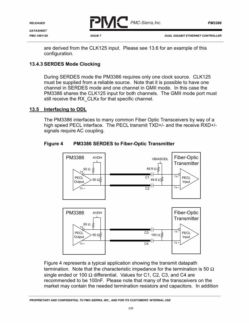
5 APPLICATION EXAMPLES
The PM3386 S/UNI-2xGE is applicable to equipment implementing high densityGigabit Ethernet interfaces. The PM3386 is a dual channel SERDES and GMACwith embedded FIFOs that provides a high density and low power GigabitEthernet solution for direct connection to electrical optical modules. Alternatively,a GMII interface is provided for connection to copper Gigabit Ethernet physicallayer devices.
On the system side, the POS-PHY Level 3 (32 bit synchronous FIFO styleinterface clocked up to 104 MHz) allows a common connection to higher layerdevices. A common system interface simplifies multi-service equipment utilizingsome or all of the following physical layer options:
• OC-48 POS/ATM
• 4xOC-12 POS/ATM
• 16xOC-3 POS/ATM
• Channelized POS/ATM
• High density DS3
• Gigabit Ethernet
The PM3386 is particularly suited for the following applications:
• Core Routers
• Edge Routers
• Enterprise Edge Routers
• Multi-Service Switches/Routers
• SONET/SDH Transport Muxes
These applications require various interfaces (Gigabit Ethernet, ATM, POS, DS3)which use the POS-PHY Level 3 interface. Service cards for various physicallayer options can re-use upper layer devices and board design to improve time-to market. The use of Gigabit Ethernet within Internet points of presence(POPs), Super POPs and Transport POPs is increasing due to the requirementof inexpensive high-speed Layer 2 interconnect. Thus, connections between
PROPRIETARY AND CONFIDENTIAL TO PMC-SIERRA, INC., AND FOR ITS CUSTOMERS’ INTERNAL USE
8
Edge Routers and Core Routers within a POP are provided via Gigabit Ethernet.Co-located server clusters are also connected via Gigabit Ethernet to POProuters. Similarly, Gigabit Ethernet is becoming the choice for connectionbetween Enterprise Routers and Multi-Service switches. Transport equipment islooking to provide Ethernet directly over SONET/SDH for wide area transparentbridging.
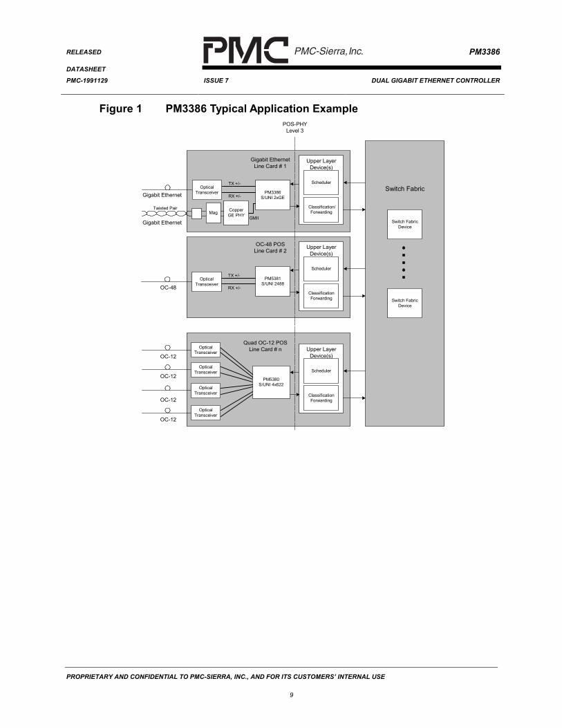
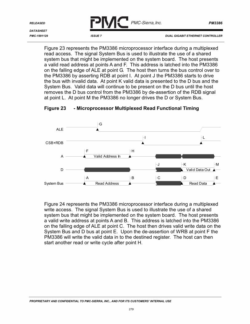
In a typical application the S/UNI-2xGE performs data recovery on the GigabitEthernet stream, MAC level frame checks and sends the frame to an upper layerdevice (such as an IP processor) for forwarding via the POS-PHY level 3interface. The S/UNI-2xGE maintains extensive statistics for SNMP and RMONapplications. On egress, frames are formatted into physical frames with theproper inter-frame gap, preamble and start of frame delimiter. The physicalpacket is then serialized for transmission over an external electrical opticalmodule. The initial configuration and ongoing control and monitoring of theS/UNI-2xGE are provided via a generic microprocessor interface. The followingdiagram shows a typical multi-service card application for the PM3386 S/UNI-2xGE with similar cards for OC48 and Quad OC-12 ports.
PROPRIETARY AND CONFIDENTIAL TO PMC-SIERRA, INC., AND FOR ITS CUSTOMERS’ INTERNAL USE
12
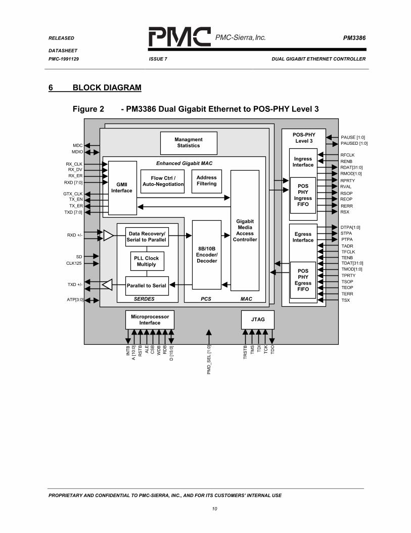
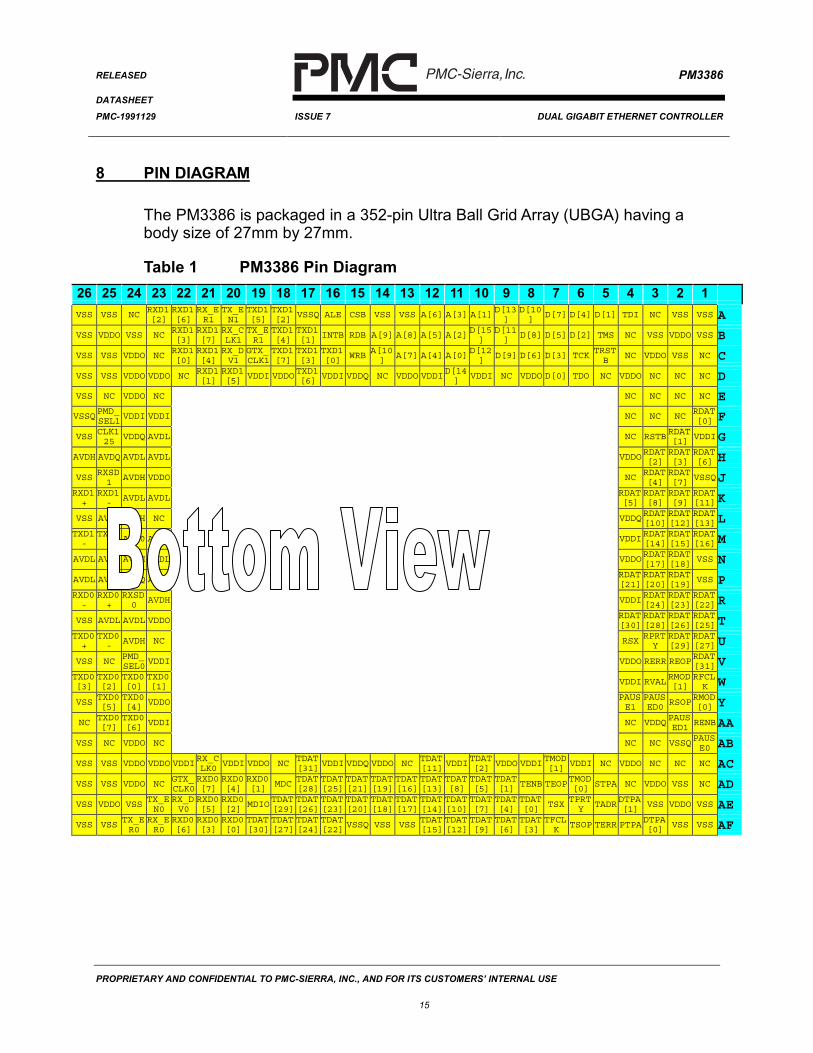
7 DESCRIPTION
The PM3386 is a monolithic integrated circuit that implements a two port fullduplex 1000 Mbit/s Gigabit Ethernet MAC data transport device. The PM3386provides line interface connectivity provided by an on-chip SERDES and GMIIfunctions and data transport to the up stream device via the industry standardPOS-PHY Level 3 interface.
Serializer-Deserializer (SERDES)
The PM3386 has two internal serializer-deserializer transceivers. The SERDESare IEEE 802.3-1998 Gigabit Ethernet compatible supporting gigabit datatransfer flows. The SERDES is based on the X3T11 10 Bit specification. ThePM3386 receives and transmits Gigabit Ethernet streams using a bit serialinterface for direct connection to optical transceiver devices. The SERDESperforms data recovery and serial to parallel conversion for connection to theEnhanced Gigabit Media Access Control block.
Gigabit Media Independent Interface (GMII)
For Gigabit Ethernet over copper support, the PM3386 provides dual standardGMII interfaces. A copper Gigabit Ethernet physical layer device can beconnected to the PM3386 via this interface.
Enhanced Gigabit Media Access Control (EGMAC)
The Enhanced Gigabit Media Access Control (EGMAC) block provides anintegrated IEEE 802.3-1998 Gigabit Ethernet Media Access Control (MAC)supporting high performance 1000Base capability. The EGMAC has line sideinterfaces for connection to internal (SERDES) and external Gigabit PHY viaGMII on each Gigabit Ethernet port. The Enhanced Gigabit MAC (EGMAC)incorporates all of the Gigabit Ethernet MAC functions including Auto-Negotiation, statistics, and the MAC Control Sub-layer that adheres to IEEE802.3-1998 providing support for PAUSE control frames. The EGMAC providesbasic frame integrity checks to validate incoming frames. The EGMAC alsoprovides simple line rate ingress address filtering support via 8 exact-match MACaddress and VID unicast filters, one 64-bin hash-based multicast filter, and theability to filter or accept matched frames on a per instance programmablefashion. All inquires for filtering are done at line rate with no system latencyintroduced for look up cycles.
PROPRIETARY AND CONFIDENTIAL TO PMC-SIERRA, INC., AND FOR ITS CUSTOMERS’ INTERNAL USE
13
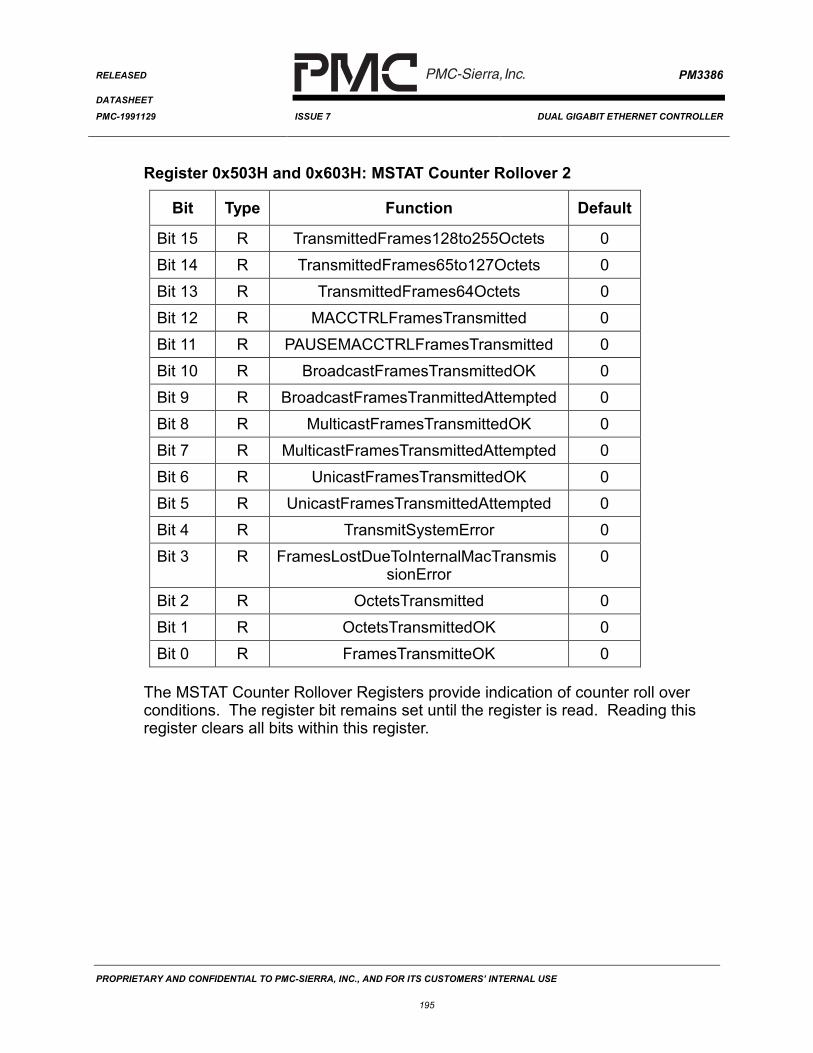
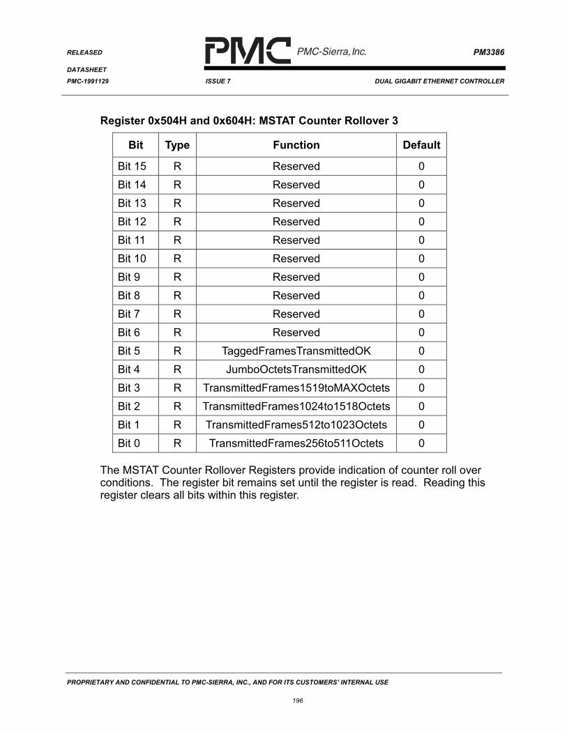
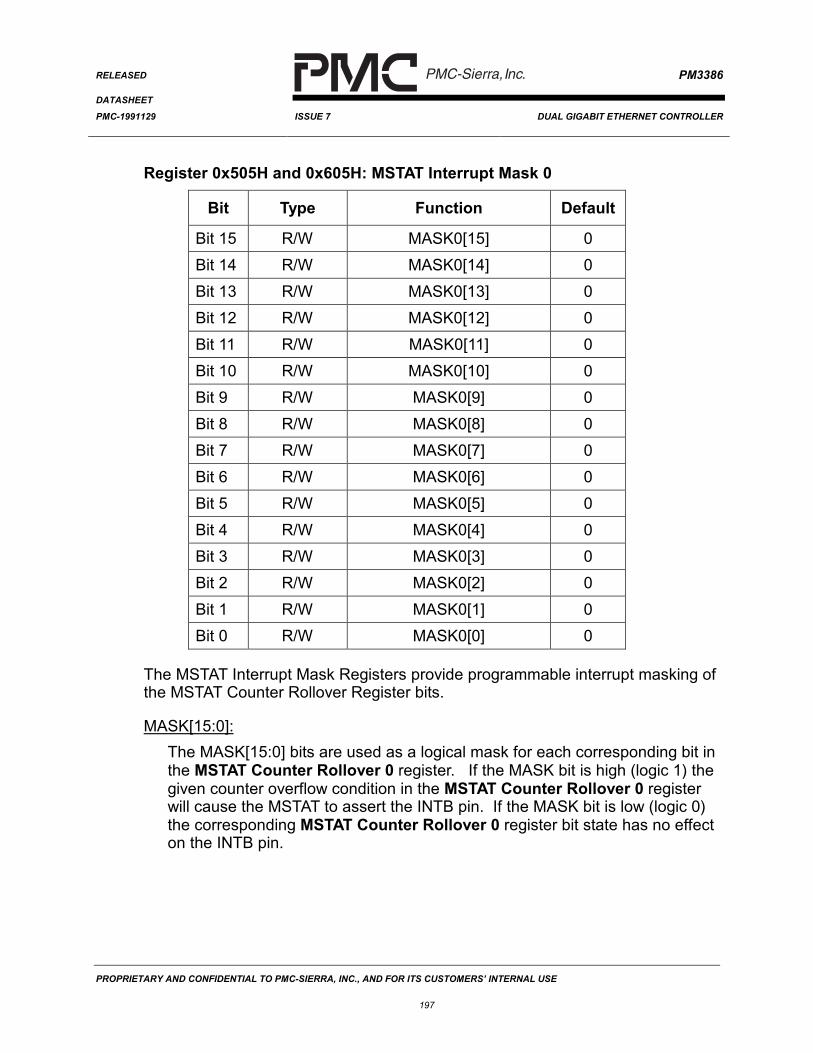
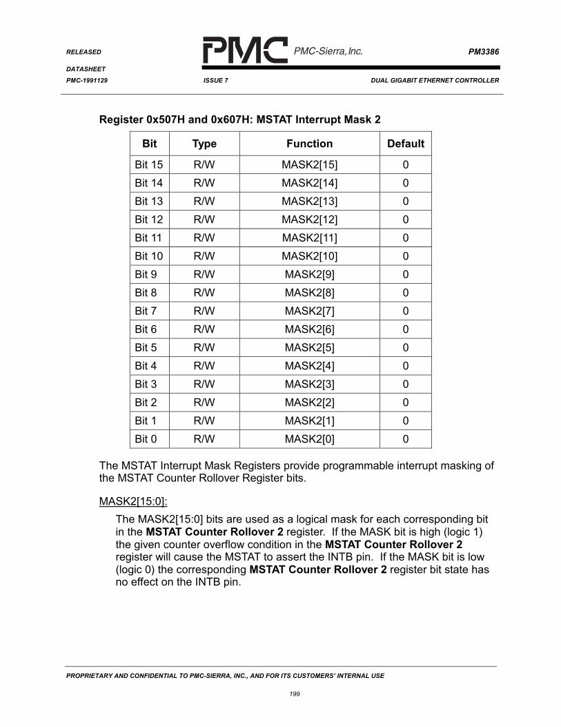
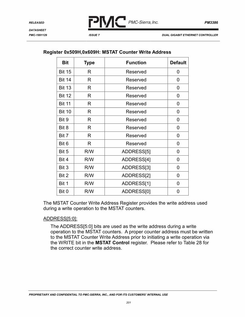
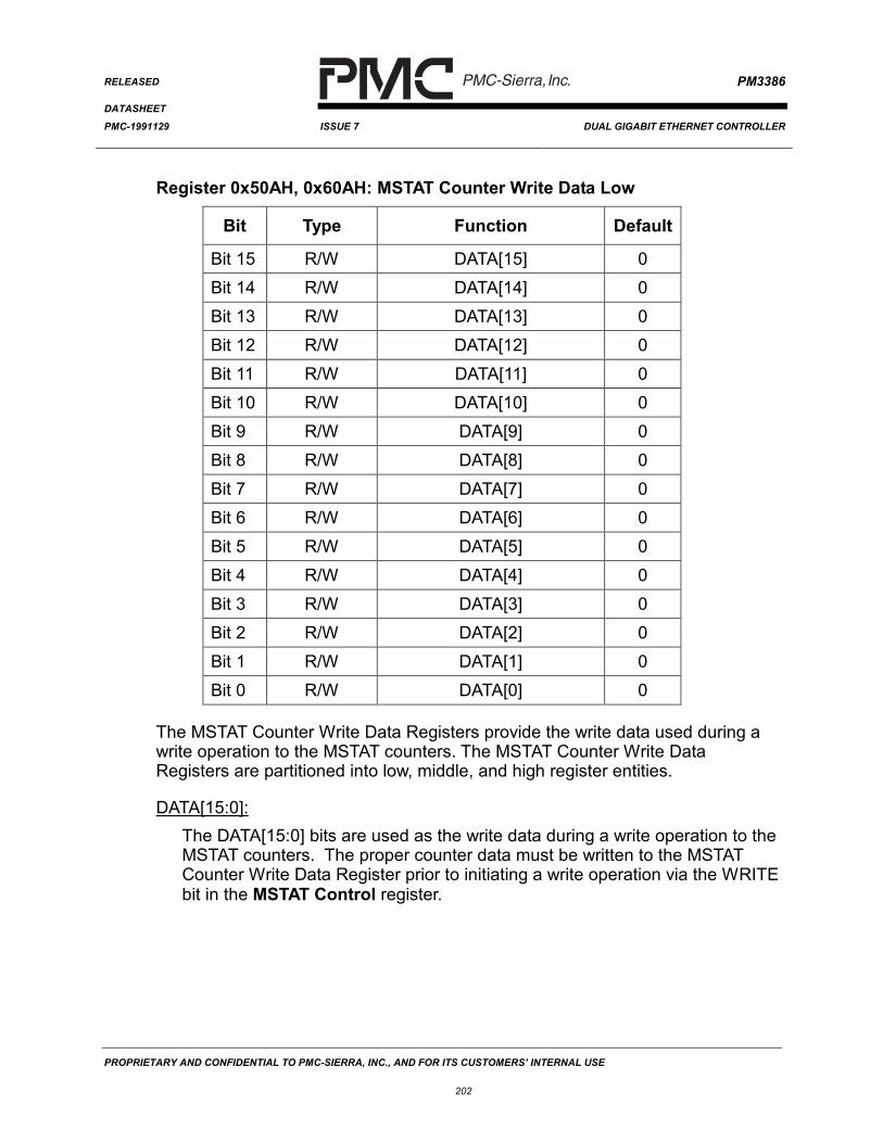
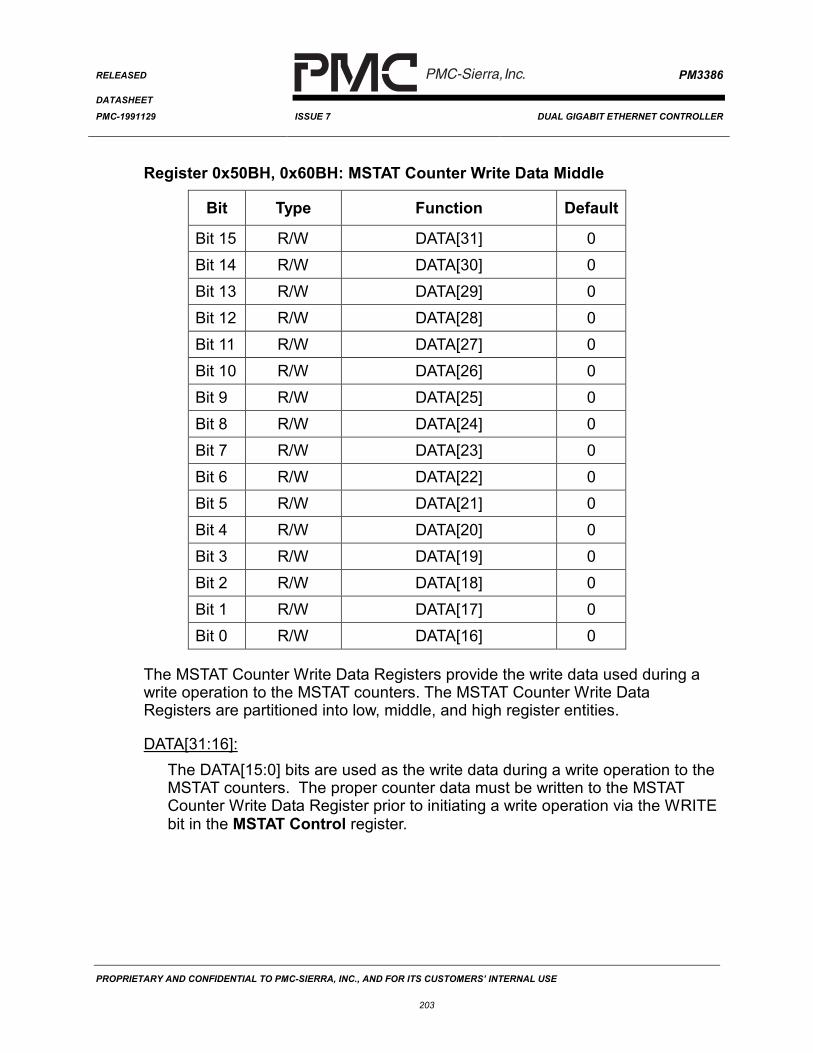
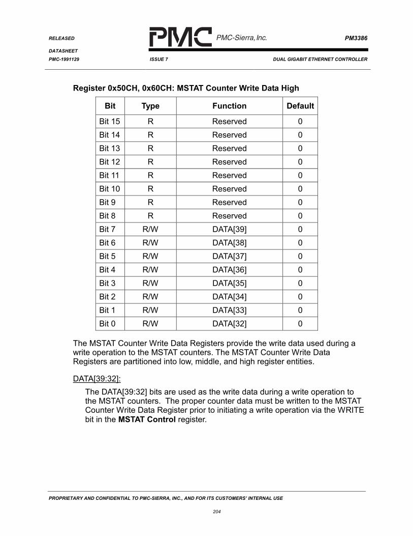
Management Statistics (MSTAT)
The PM3386 also incorporates a rich set of per port RMON, SNMP, and EtherlikeManagement Information Base counters. Deep statistical counters are used formanagement counts providing a minimum rollover time of greater than 58minutes. All counts are easily managed via the Management Statistics (MSTAT)block.
POS-PHY Level 3 Interface (PL3)
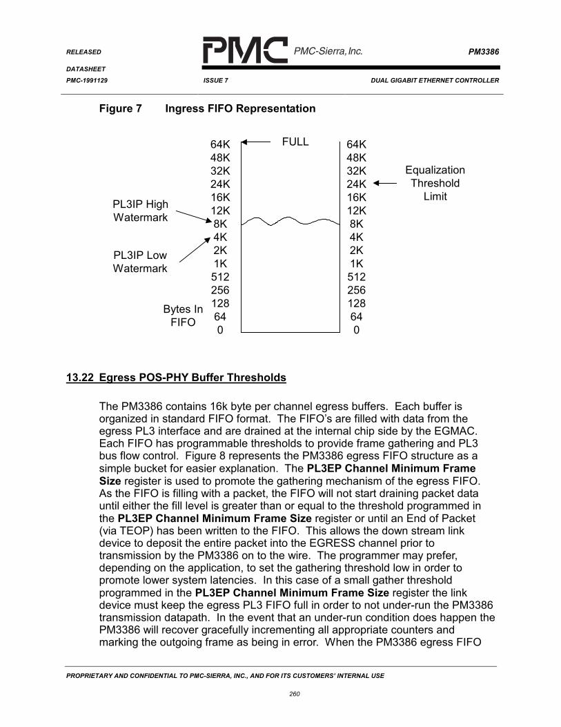
The PM3386 can connect to a single upper layer device through a POS-PHYLevel 3 Interface. The POS-PHY Level 3 interface is a 32-bit wide interface witha clock rate from 60 to 104 MHz. POS-PHY Level 3 was developed with thecooperation of the SATURN Development Group to cover all application bit ratesup to and including 3.2 Gbit/s. This interface provides standards support forinteroperation between the PM3386, a multiple PHY layer device, connecting toone Link Layer device. The interface stresses simplicity of operation to allowforward migration to more elaborate PHY and Link Layer devices. The POS-PHY interface contains 64KB receive and 16KB transmit FIFOs per channel.These FIFOs contain programmable thresholds specifying full and emptyconditions.
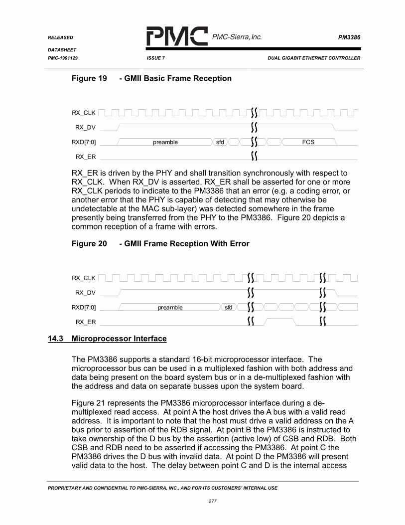
Receive Direction
In the receive direction, the PM3386 can be configured to use the internalSERDES or the GMII interface on a per channel basis. For SERDES operation,a Gigabit Ethernet bit stream is received from an external optical transceiver.The data is recovered and converted from serial to parallel data for connection tothe EGMAC block. The EGMAC terminates the 8B/10B line codes and performsframe integrity checks (frame length, FCS etc). For GMII operation, the physicalpacket is sourced from an external copper physical layer device to the PM3386via the GMII interface (8 bits clocked at 125 MHz). The EGMAC accepts the 8 bitdata and performs frame integrity checks once the complete frame is received.The EGMAC can optionally filter erred frames.
Statistics are updated and the frame is sent to the POS-PHY Level 3 interface.The FIFO’s in the POS-PHY interface accommodate system latencies and allowsfor loss-less flow control up to 9.6k bytes. The received frames are then readthrough the POS-PHY Level 3 (32 bits clocked from 60-104 MHz) system sideinterface.
Transmit Direction
In the transmit direction, packets to be transmitted are written into the POS-PHYTX FIFO through the POS-PHY Level 3 interface (32 bits clocked from 60-104
PROPRIETARY AND CONFIDENTIAL TO PMC-SIERRA, INC., AND FOR ITS CUSTOMERS’ INTERNAL USE
14
MHz) from the upper layer device. The channel is selected by the upper layerdevice and is indicated in-band on the POS-PHY interface. The EGMAC builds aproperly formatted Ethernet physical packet (padding to minimum size andinserting the preamble, start of frame delimiter (SFD) and the inter-packet gap(IPG)). Statistics are updated and the physical packet is sent to the SERDES orthe GMII interface.
For SERDES operation, the EGMAC encodes the physical packet using 8B/10Bencoding and passes the physical packet to the SERDES block. The SERDESperforms parallel to serial conversion using an internally synthesized 1250 MHzclock. The bit stream is sent to an external optical transceiver for transmissionover fiber cable. For GMII operation, the EGMAC sends the physical packet byteby byte across the GMII interface (8 bits clocked at 125 MHz) to an externalcopper Gigabit Ethernet physical layer device. The copper Gigabit Ethernetphysical layer device then transmits the physical packet over copper cable.
Flow Control
Flow control is handled in the EGMAC block. When a PAUSE control frame isreceived, the PM3386 will optionally terminate transmission (after the currentframe is sent) and assert the appropriate channel side band flow control outputto indicate the paused condition. The received PAUSE control frame can beoptionally filtered or passed to the link layer device via the POS-PHY Level 3interface.
PAUSE control frames are transmitted either under link layer control usingchannel side band flow control inputs, under link layer control transparent to thePM3386, host based PAUSE frame control or under internal control based onreceive FIFO levels. All four methods can provide for loss-less flow control.
General
The PM3386 is configured, controlled and monitored via a generic 16-bitmicroprocessor bus interface. The PM3386 also provides a standard 5 signalIEEE 1149.1 JTAG test port for boundary scan board test purposes.The PM3386 is implemented in low power, +1.8 Volt, CMOS technology with 5VTTL compatible digital inputs and 3.3V TTL/CMOS compatible digital outputs.The PM3386 is packaged in a 352-pin UBGA package.
PROPRIETARY AND CONFIDENTIAL TO PMC-SIERRA, INC., AND FOR ITS CUSTOMERS’ INTERNAL USE
16
9 PIN DESCRIPTION
Table 2 - Serial Line Side Interface Signals
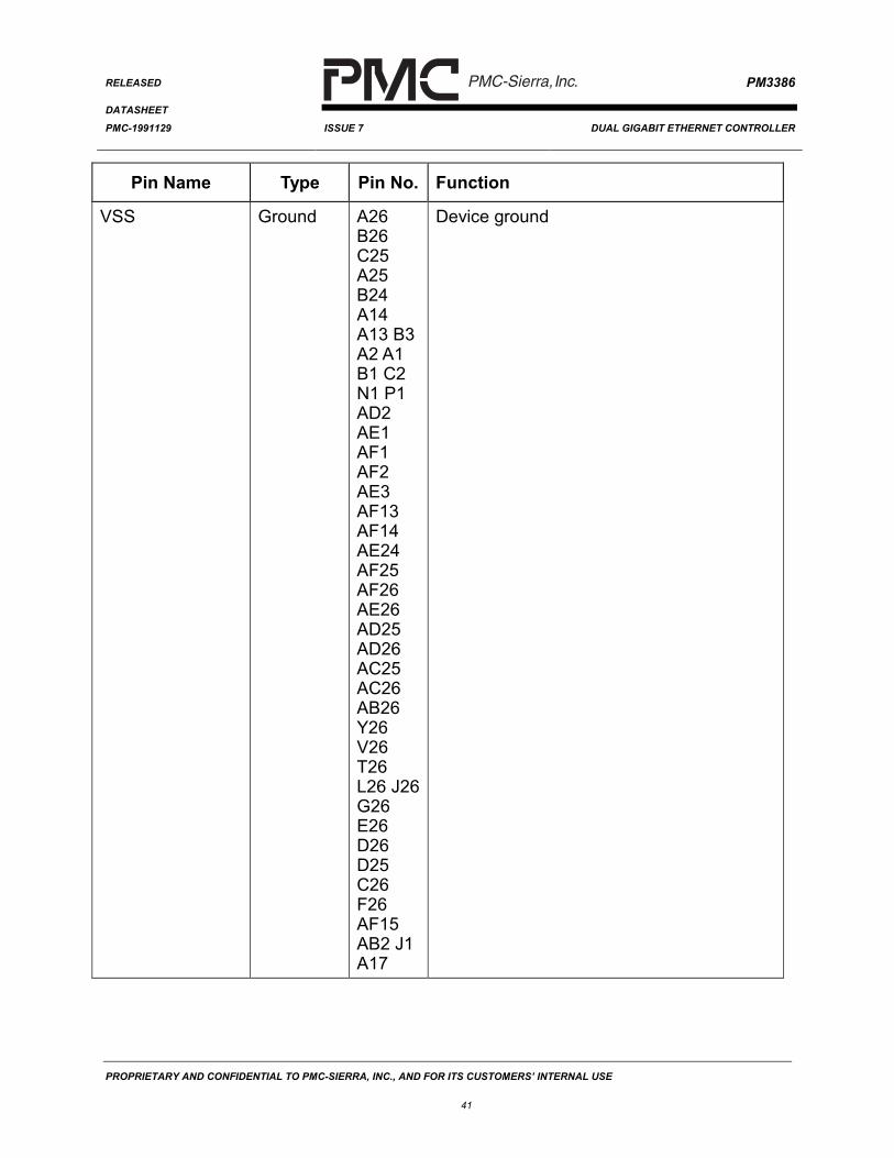
Pin Name Type Pin No. Function
CLK125 SchmittInput
G25 PHY Reference Clock (Port 0)125 MHz reference clock used to generateGTX_CLK0 or GTX_CLK1 during GMIImode. The Clock Synthesis Unit uses thisclock as it’s input reference duringSERDES mode.Please refer to the Operations section for adiscussion of clock mode selectioninterfacing issues.
RXD0+RXD0-
DifferentialPECLInput
R25R26
Receive Differential Data (Port 0)These PECL inputs (RXD0+/-) contain the8B/10B bit serial receive stream. Thereceive data is recovered from the RXD0+/-bit stream.
RXSD0 Input R24 Receive Signal Detect (Port 0)RXSD0 indicates the presence of validreceive signal power from the OpticalPhysical Medium Dependent Device. Alogic level high indicates the presence ofvalid data. A logic low indicates a loss ofsignal.
RXD1+RXD1-
DifferentialPECLInput
K26K25
Receive Differential Data (Port 1)The PECL inputs RXD1+/- contain the8B/10B bit serial receive stream. Thereceive data is recovered from the RXD1+/-bit stream.
PROPRIETARY AND CONFIDENTIAL TO PMC-SIERRA, INC., AND FOR ITS CUSTOMERS’ INTERNAL USE
17
Pin Name Type Pin No. Function
RXSD1 Input J25 Receive Signal Detect (Port 1)RXSD1 indicates the presence of validreceive signal power from the OpticalPhysical Medium Dependent Device. Alogic level high indicates the presence ofvalid data. A logic low indicates a loss ofsignal.
TXD0+TXD0-
DifferentialPECLOutput
U26U25
Transmit Differential Data (Port 0)The PECL outputs TXD0+/- contain the1.25 Gbit/s transmit stream. The TXD0+/-outputs are driven using the CSU clock.
TXD1+TXD1-
DifferentialPECLOutput
M25M26
Transmit Differential Data (Port 1)The PECL outputs TXD1+/- contain the1.25 Gbit/s transmit stream. The TXD1+/-outputs are driven using the CSU clock.
ATP0ATP1
Bi-DirectionalCMOS
M24M23
Receive and Transmit Analog Test PortsThe ATP[1:0] pins are used formanufacturing testing only and should betied to analog ground.
Table 3 -Gigabit Media Independent Interface (GMII)
Signal Name Direction Pin No. FunctionGTX_CLK0 Output AD22 GMII Transmit Clock (Port 0)
GMII Transmit Data (Port 0)Byte-wide transmit data is output on thesepins synchronously to the PHY device.The least significant bit, TXD0[0] is the firstbit transferred on the line.This signal is updated on the rising edge ofGTX_CLK0.
PROPRIETARY AND CONFIDENTIAL TO PMC-SIERRA, INC., AND FOR ITS CUSTOMERS’ INTERNAL USE
18
Signal Name Direction Pin No. FunctionTX_EN0 Output AE23 Transmit Enable (Port 0)
When in GMII mode this signal is an activehigh signal asserted when valid data ispresent on the TXD0[7:0] and TX_ER0pins. This signal is updated on the risingedge of GTX_CLK0.When in SERDES mode this signalenables operation of the externaltransmitter. When asserted (default activelow) it indicates the potential presence ofvalid transmit data. When de-assertedindicates the absence of valid transmitdata. Note that while in SERDES modethe polarity of this signal is programmableto support interoperability with differingoptical transmitters.
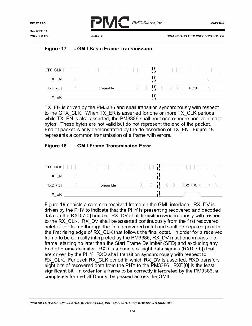
TX_ER0 Output AF24 GMII Transmit Coding Error (Port 0)Active high signal asserted when an erroris detected during transmission. Pleaserefer to the Operations section for a fulllisting of error conditions reported by thePM3386 using the TX_ER0 output.This signal is updated on the rising edge ofGTX_CLK0.
GMII Receive Data (Port 0)Byte-wide receive data is input on thesepins synchronously from the PHY device.The least significant bit, RXD0[0] isexpected to contain the first bit received onthe line.This signal is synchronized to RX_CLK0.
PROPRIETARY AND CONFIDENTIAL TO PMC-SIERRA, INC., AND FOR ITS CUSTOMERS’ INTERNAL USE
19
Signal Name Direction Pin No. FunctionRX_DV0 Input AE22 GMII Receive Data Valid (Port 0)
Active high signal asserted when valid datais present on the RXD0[7:0] and RX_ER0pins.This signal is synchronized to RX_CLK0.
RX_ER0 Input AF23 GMII Receive Error (Port 0)Active high signal asserted when there hasbeen an error during the received physicalpacket.This signal is synchronized to RX_CLK0.
GMII Transmit Data (Port 1)Byte-wide transmit data is output on thesepins synchronously to the PHY device.The least significant bit, TXD1[0] is the firstbit transferred on the line.This signal is updated on the rising edge ofGTX_CLK1.
PROPRIETARY AND CONFIDENTIAL TO PMC-SIERRA, INC., AND FOR ITS CUSTOMERS’ INTERNAL USE
20
Signal Name Direction Pin No. FunctionTX_EN1 Output A20 Transmit Enable (Port 1)
When in GMII mode this signal is an activehigh signal asserted when valid data ispresent on the TXD1[7:0] and TX_ER1pins. This signal is updated on the risingedge of GTX_CLK1.When in SERDES mode this signalenables operation of the externaltransmitter. When asserted (default activelow) it indicates the potential presence ofvalid transmit data. When de-assertedindicates the absence of valid transmitdata. Note that while in SERDES modethe polarity of this signal is programmableto support interoperability with differingoptical transmitters.
TX_ER1 Output B19 GMII Transmit Coding Error (Port 1)Active high signal asserted when an erroris detected during transmission. Pleaserefer to the Operations section for a fulllisting of error conditions reported by thePM3386 using the TX_ER1 output. Thissignal is updated on the rising edge ofGTX_CLK1.
GMII Receive Data (Port 1)Byte-wide receive data is input on thesepins synchronously from the PHY device.The least significant bit, RXD1[0] isexpected to contain the first bit received onthe line.This signal is synchronized to RX_CLK1.
PROPRIETARY AND CONFIDENTIAL TO PMC-SIERRA, INC., AND FOR ITS CUSTOMERS’ INTERNAL USE
21
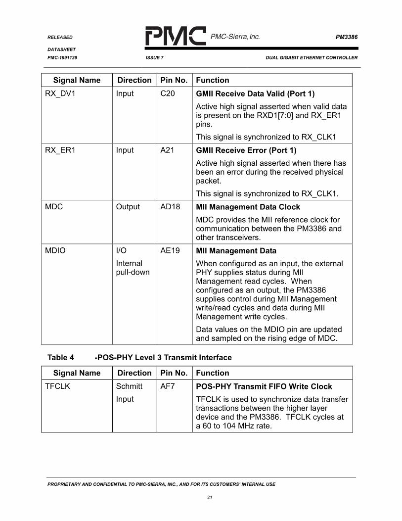
Signal Name Direction Pin No. FunctionRX_DV1 Input C20 GMII Receive Data Valid (Port 1)
Active high signal asserted when valid datais present on the RXD1[7:0] and RX_ER1pins.This signal is synchronized to RX_CLK1
RX_ER1 Input A21 GMII Receive Error (Port 1)Active high signal asserted when there hasbeen an error during the received physicalpacket.This signal is synchronized to RX_CLK1.
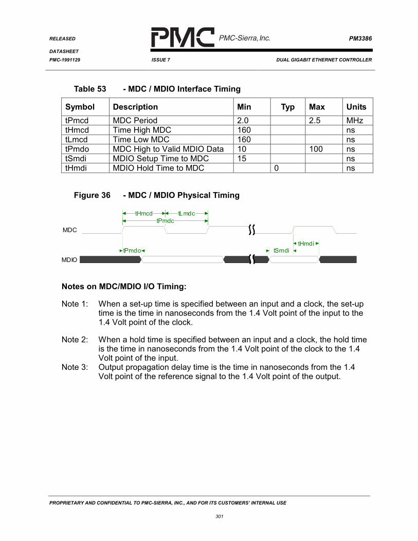
MDC Output AD18 MII Management Data ClockMDC provides the MII reference clock forcommunication between the PM3386 andother transceivers.
MDIO I/OInternalpull-down
AE19 MII Management DataWhen configured as an input, the externalPHY supplies status during MIIManagement read cycles. Whenconfigured as an output, the PM3386supplies control during MII Managementwrite/read cycles and data during MIIManagement write cycles.Data values on the MDIO pin are updatedand sampled on the rising edge of MDC.
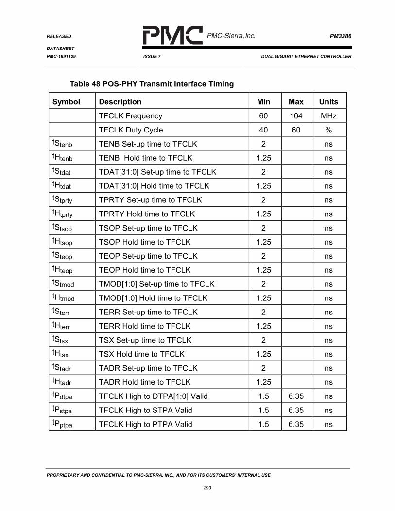
Table 4 -POS-PHY Level 3 Transmit Interface
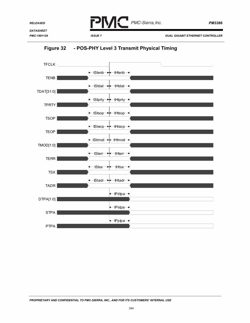
Signal Name Direction Pin No. FunctionTFCLK Schmitt
InputAF7 POS-PHY Transmit FIFO Write Clock
TFCLK is used to synchronize data transfertransactions between the higher layerdevice and the PM3386. TFCLK cycles ata 60 to 104 MHz rate.
PROPRIETARY AND CONFIDENTIAL TO PMC-SIERRA, INC., AND FOR ITS CUSTOMERS’ INTERNAL USE
22
Signal Name Direction Pin No. FunctionTDAT[0]TDAT[1]TDAT[2]TDAT[3]TDAT[4]TDAT[5]TDAT[6]TDAT[7]TDAT[8]TDAT[9]TDAT[10]TDAT[11]TDAT[12]TDAT[13]TDAT[14]TDAT[15]TDAT[16]TDAT[17]TDAT[18]TDAT[19]TDAT[20]TDAT[21]TDAT[22]TDAT[23]TDAT[24]TDAT[25]TDAT[26]TDAT[27]TDAT[28]TDAT[29]TDAT[30]TDAT[31]
POS-PHY Transmit Packet Data BusThis bus carries the packet octets that arewritten to the selected transmit FIFO andthe in-band port address to select thedesired transmit FIFO. The TDAT bus isconsidered valid only when TENB issimultaneously asserted.When a 32-bit interface is used, data mustbe transmitted in big endian order onTDAT[31:0].TDAT[31:0] is sampled on the rising edgeof TFCLK.
PROPRIETARY AND CONFIDENTIAL TO PMC-SIERRA, INC., AND FOR ITS CUSTOMERS’ INTERNAL USE
23
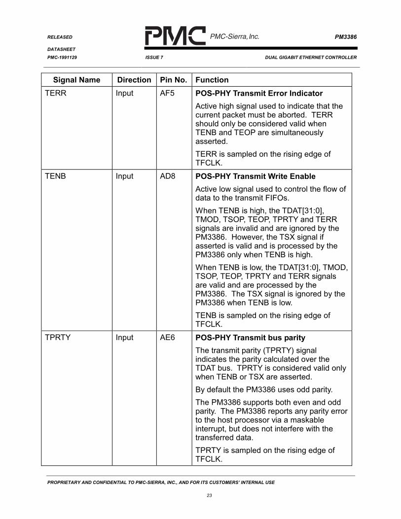
Signal Name Direction Pin No. FunctionTERR Input AF5 POS-PHY Transmit Error Indicator
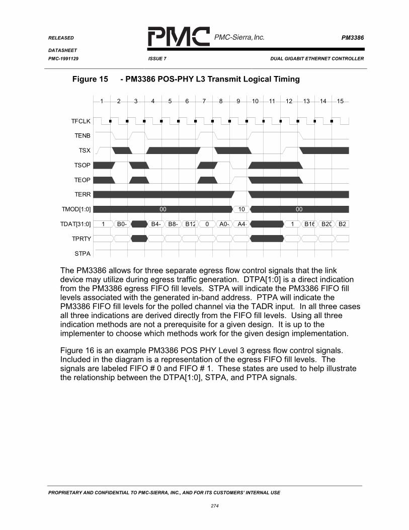
Active high signal used to indicate that thecurrent packet must be aborted. TERRshould only be considered valid whenTENB and TEOP are simultaneouslyasserted.TERR is sampled on the rising edge ofTFCLK.
TENB Input AD8 POS-PHY Transmit Write EnableActive low signal used to control the flow ofdata to the transmit FIFOs.When TENB is high, the TDAT[31:0],TMOD, TSOP, TEOP, TPRTY and TERRsignals are invalid and are ignored by thePM3386. However, the TSX signal ifasserted is valid and is processed by thePM3386 only when TENB is high.When TENB is low, the TDAT[31:0], TMOD,TSOP, TEOP, TPRTY and TERR signalsare valid and are processed by thePM3386. The TSX signal is ignored by thePM3386 when TENB is low.TENB is sampled on the rising edge ofTFCLK.
TPRTY Input AE6 POS-PHY Transmit bus parityThe transmit parity (TPRTY) signalindicates the parity calculated over theTDAT bus. TPRTY is considered valid onlywhen TENB or TSX are asserted.By default the PM3386 uses odd parity.The PM3386 supports both even and oddparity. The PM3386 reports any parity errorto the host processor via a maskableinterrupt, but does not interfere with thetransferred data.TPRTY is sampled on the rising edge ofTFCLK.
PROPRIETARY AND CONFIDENTIAL TO PMC-SIERRA, INC., AND FOR ITS CUSTOMERS’ INTERNAL USE
24
Signal Name Direction Pin No. FunctionTMOD[0]TMOD[1]
Input AD6AC7
POS-PHY Transmit Word ModuloTMOD[1:0] indicates the number of validbytes of data in TDAT[31:0]. The TMODbus should always be all zero, exceptduring the last double-word transfer of apacket on TDAT[31:0]. When TEOP andTENB are asserted, the number of validpacket data bytes on TDAT[31:0] isspecified by TMOD[1:0].TMOD[1:0] = “00” TDAT[31:0] validTMOD[1:0] = “01” TDAT[31:8] validTMOD[1:0] = “10” TDAT[31:16] validTMOD[1:0] = “11” TDAT[31:24] validTMOD [1:0] is sampled on the rising edgeof TFCLK.
TSX Input AE7 POS-PHY Transmit Start of TransferActive high signal indicating when the in-band port address is present on theTDAT[31:0] bus. When TSX is high andTENB is high (not asserted), the value ofcontained within TDAT[7:0] is the addressof the transmit FIFO to be selected.TDAT[7:0] == 0 selects channel zero.TDAT[7:0] == 1 selects channel one.Subsequent data transfers on the TDATbus will fill the FIFO specified by this in-band address.If TDAT[7:0] is not 0 or 1 no channel withinthe PM3386 device will be selected.Subsequent data transfers on the TDATbus to address outside of 0 or 1 will bedropped at the PL3 interface.TSX is considered valid only when TENB isnot asserted.TSX is sampled on the rising edge ofTFCLK.
PROPRIETARY AND CONFIDENTIAL TO PMC-SIERRA, INC., AND FOR ITS CUSTOMERS’ INTERNAL USE
25
Signal Name Direction Pin No. FunctionTSOP Input AF6 POS-PHY Transmit Start of Packet
Active high signal used to delineate thepacket boundaries on the TDAT bus.When TSOP is high, the start of the packetis present on the TDAT bus.TSOP is required to be present at thebeginning of every packet and isconsidered valid only when TENB isasserted.TSOP is sampled on the rising edge ofTFCLK.
TEOP Input AD7 POS-PHY Transmit End of PacketActive high signal used to delineate thepacket boundaries on the TDAT bus.When TEOP is high, the end of the packetis present on the TDAT bus.Note that TMOD[1:0] indicates the numberof valid bytes the last double word iscomposed of when TEOP and TENB areasserted.TEOP is required to be present at the endof every packet and is considered valid onlywhen TENB is asserted.TEOP is sampled on the rising edge ofTFCLK.
PROPRIETARY AND CONFIDENTIAL TO PMC-SIERRA, INC., AND FOR ITS CUSTOMERS’ INTERNAL USE
26
Signal Name Direction Pin No. FunctionTADR Input AE5 POS-PHY Transmit PHY Address
The TADR signal is used with the PTPAsignal to poll the transmit FIFOs packetavailable status.When TADR is sampled on the rising edgeof TFCLK by the PM3386, the polledpacket available indication PTPA signal isupdated with the status of the port specifiedby the TADR address on the following risingedge of TFCLK.TADR = 0 = channel 0TADR = 1 = channel 1TADR is sampled on the rising edge ofTFCLK.
PTPA Output AF4 POS-PHY Polled-PHY Transmit PacketAvailablePTPA transitions high when a predefined(user programmable) minimum number ofbytes are available in the polled transmitFIFO. Once high, PTPA indicates that thetransmit FIFO is not full. When PTPAtransitions low, it indicates that the transmitFIFO is full or near full (userprogrammable).PTPA allows the polling of the PM3386channel selected by TADR address pin.The port which PTPA reports is updated onthe following rising edge of TFCLK after thePM3386 channel address on TADR issampled by the PM3386 device.PTPA is updated on the rising edge ofTFCLK.
PROPRIETARY AND CONFIDENTIAL TO PMC-SIERRA, INC., AND FOR ITS CUSTOMERS’ INTERNAL USE
27
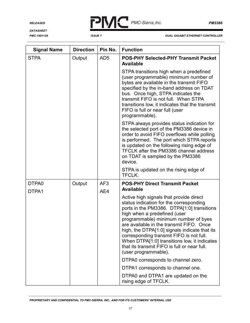
Signal Name Direction Pin No. FunctionSTPA Output AD5 POS-PHY Selected-PHY Transmit Packet
AvailableSTPA transitions high when a predefined(user programmable) minimum number ofbytes are available in the transmit FIFOspecified by the in-band address on TDATbus. Once high, STPA indicates thetransmit FIFO is not full. When STPAtransitions low, it indicates that the transmitFIFO is full or near full (userprogrammable).STPA always provides status indication forthe selected port of the PM3386 device inorder to avoid FIFO overflows while pollingis performed. The port which STPA reportsis updated on the following rising edge ofTFCLK after the PM3386 channel addresson TDAT is sampled by the PM3386device.STPA is updated on the rising edge ofTFCLK.
DTPA0DTPA1
Output AF3AE4
POS-PHY Direct Transmit PacketAvailableActive high signals that provide directstatus indication for the correspondingports in the PM3386. DTPA[1:0] transitionshigh when a predefined (userprogrammable) minimum number of byesare available in the transmit FIFO. Oncehigh, the DTPA[1:0] signals indicate that itscorresponding transmit FIFO is not full.When DTPA[1:0] transitions low, it indicatesthat its transmit FIFO is full or near full.(user programmable).DTPA0 corresponds to channel zero.DTPA1 corresponds to channel one.DTPA0 and DTPA1 are updated on therising edge of TFCLK.
PROPRIETARY AND CONFIDENTIAL TO PMC-SIERRA, INC., AND FOR ITS CUSTOMERS’ INTERNAL USE
28
Table 5 - POS-PHY Level 3 Receive Interface
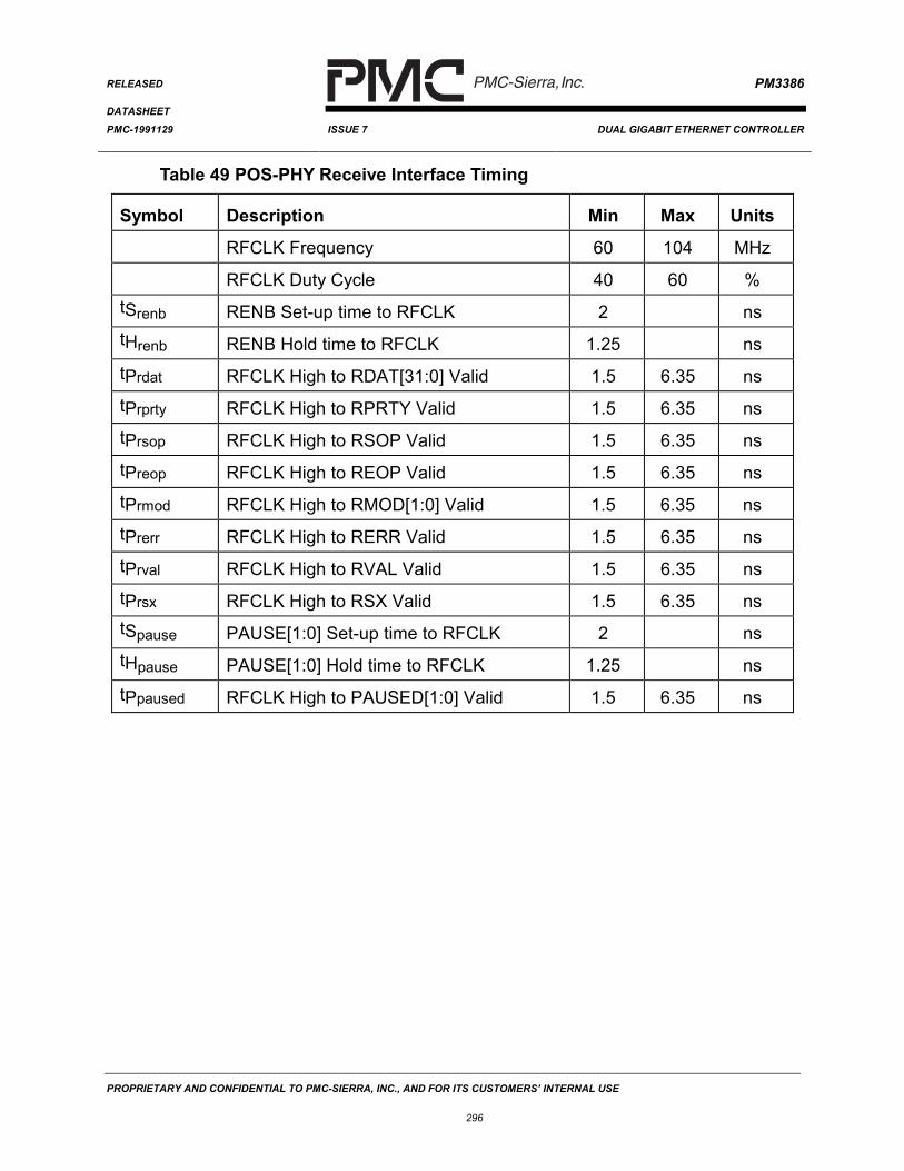
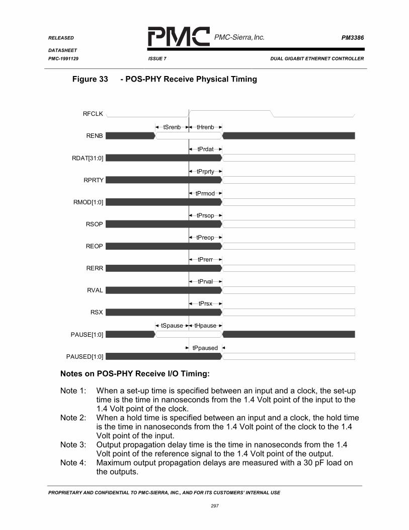
Signal Name Direction Pin No. FunctionRFCLK Schmitt
InputW1 POS-PHY Receive FIFO Write Clock
RFCLK is used to synchronize datatransfer transactions between the higherlayer device and the PM3386. RFCLKcycles at a rate of 60 to 104 MHz.
RVAL Output W3 POS-PHY Receive Data ValidActive high signal indicating the validity ofthe receive data signals. RVAL willtransition low when a receive FIFO isempty, at the end of a data burst from agiven channel.When RVAL is high, the RDAT[31:0],RPRTY, RMOD[1:0], RSOP, REOP andRERR signals are valid. When RVAL islow, the RDAT[31:0], RPRTY, RMOD[1:0],RSOP, REOP and RERR signals areinvalid and must be disregarded.The RSX signal is only valid when RVAL islow.RVAL is updated on the rising edge ofRFCLK.
PROPRIETARY AND CONFIDENTIAL TO PMC-SIERRA, INC., AND FOR ITS CUSTOMERS’ INTERNAL USE
29
Signal Name Direction Pin No. FunctionRENB Input AA1 POS-PHY Receive Read Enable
Active low signal used to control the flow ofdata from the PM3386.The higher layer device may de-assertRENB at anytime if it is unable to acceptdata from the PM3386.When RENB is sampled low by thePM3386, the upper level device is signalingthat it can receive data.RSX may then be asserted to indicate anew address on the RDAT[0] bus pin orRVAL may be asserted indicating validity ofread data and control on the RDAT[31:0],RPRTY, RMOD[1:0], RSOP, REOP, andRERR signals. Note that these signals willbe updated on the following rising edge ofthe RFCLK.When RENB is sampled high by thePM3386, the upper level device is signalingthat it can no longer accept data.On the following rising edge of RFCLK, ifactive, the RVAL signal will remainasserted signifying valid data and controlon RDAT[31:0], RPRTY, RMOD[1:0],RSOP, REOP, and RERR.RENB is sampled on the rising edge ofRFCLK.
PROPRIETARY AND CONFIDENTIAL TO PMC-SIERRA, INC., AND FOR ITS CUSTOMERS’ INTERNAL USE
30
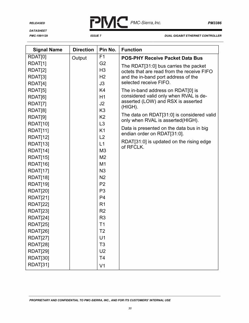
Signal Name Direction Pin No. FunctionRDAT[0]RDAT[1]RDAT[2]RDAT[3]RDAT[4]RDAT[5]RDAT[6]RDAT[7]RDAT[8]RDAT[9]RDAT[10]RDAT[11]RDAT[12]RDAT[13]RDAT[14]RDAT[15]RDAT[16]RDAT[17]RDAT[18]RDAT[19]RDAT[20]RDAT[21]RDAT[22]RDAT[23]RDAT[24]RDAT[25]RDAT[26]RDAT[27]RDAT[28]RDAT[29]RDAT[30]RDAT[31]
POS-PHY Receive Packet Data BusThe RDAT[31:0] bus carries the packetoctets that are read from the receive FIFOand the in-band port address of theselected receive FIFO.The in-band address on RDAT[0] isconsidered valid only when RVAL is de-asserted (LOW) and RSX is asserted(HIGH).The data on RDAT[31:0] is considered validonly when RVAL is asserted(HIGH).Data is presented on the data bus in bigendian order on RDAT[31:0].RDAT[31:0] is updated on the rising edgeof RFCLK.
PROPRIETARY AND CONFIDENTIAL TO PMC-SIERRA, INC., AND FOR ITS CUSTOMERS’ INTERNAL USE
31
Signal Name Direction Pin No. FunctionRPRTY Output U3 POS-PHY Receive Parity
The receive parity (RPRTY) signalindicates the parity calculated over theRDAT bus. RPRTY is only valid whenRVAL or RSX is asserted. The PM3386supports both odd and even parity over theRDAT bus.RPRTY is updated on the rising edge ofRFCLK.
RMOD[0]RMOD[1]
Output Y1W2
POS-PHY Receive Word ModuloRMOD[1:0] indicates the number of validbytes of data in RDAT[31:0]. The RMODbus must always be zero, except during thelast double-word transfer of a packet onRDAT[31:0]. When REOP and RVAL areasserted, the number of valid packet databytes on RDAT[31:0] is specified byRMOD[1:0].RMOD[1:0] = “00” RDAT[31:0] validRMOD[1:0] = “01” RDAT[31:8] validRMOD[1:0] = “10” RDAT[31:16] validRMOD[1:0] = “11” RDAT[31:24] validRMOD[1:0] is considered valid only whenRVAL and REOP are asserted.RMOD[1:0] is updated on the rising edge ofRFCLK.
RSOP Output Y2 POS-PHY Receive Start of PacketActive high signal used to delineate thepacket boundaries on the RDAT bus.When RSOP is high, the start of the packetis present on the RDAT bus.RSOP is required to be present at the startof every packet and is only consideredvalid when RVAL is asserted.RSOP is updated on the rising edge ofRFCLK.
PROPRIETARY AND CONFIDENTIAL TO PMC-SIERRA, INC., AND FOR ITS CUSTOMERS’ INTERNAL USE
32
Signal Name Direction Pin No. FunctionREOP Output V2 POS-PHY Receive End Of Packet
Active high signal used to delineate thepacket boundaries on the RDAT bus.When REOP is high, the end of the packetis present on the RDAT bus.Note that RMOD[1:0] indicates the numberof valid bytes the last double word iscomposed of when REOP and RVAL areasserted.REOP is required to be present at the endof every packet and is considered validonly when RVAL is asserted.REOP is updated on the rising edge ofRFCLK.
RERR Output V3 POS-PHY Receive error indicatorActive high signal used to indicate that thecurrent packet is aborted and should bediscarded. RERR shall only be assertedwhen REOP and RVAL are asserted.Conditions that can cause RERR to be setmay be, but are not limited to, FIFOoverflow, abort sequence detection andFCS error.RERR is updated on the rising edge ofRFCLK.
PROPRIETARY AND CONFIDENTIAL TO PMC-SIERRA, INC., AND FOR ITS CUSTOMERS’ INTERNAL USE
33
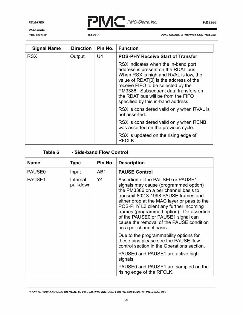
Signal Name Direction Pin No. FunctionRSX Output U4 POS-PHY Receive Start of Transfer
RSX indicates when the in-band portaddress is present on the RDAT bus.When RSX is high and RVAL is low, thevalue of RDAT[0] is the address of thereceive FIFO to be selected by thePM3386. Subsequent data transfers onthe RDAT bus will be from the FIFOspecified by this in-band address.RSX is considered valid only when RVAL isnot asserted.RSX is considered valid only when RENBwas asserted on the previous cycle.RSX is updated on the rising edge ofRFCLK.
Table 6 - Side-band Flow Control
Name Type Pin No. Description
PAUSE0PAUSE1
InputInternalpull-down
AB1Y4
PAUSE ControlAssertion of the PAUSE0 or PAUSE1signals may cause (programmed option)the PM3386 on a per channel basis totransmit 802.3-1998 PAUSE frames andeither drop at the MAC layer or pass to thePOS-PHY L3 client any further incomingframes (programmed option). De-assertionof the PAUSE0 or PAUSE1 signal cancause the removal of the PAUSE conditionon a per channel basis.Due to the programmability options forthese pins please see the PAUSE flowcontrol section in the Operations section.PAUSE0 and PAUSE1 are active highsignals.PAUSE0 and PAUSE1 are sampled on therising edge of the RFCLK.
PROPRIETARY AND CONFIDENTIAL TO PMC-SIERRA, INC., AND FOR ITS CUSTOMERS’ INTERNAL USE
34
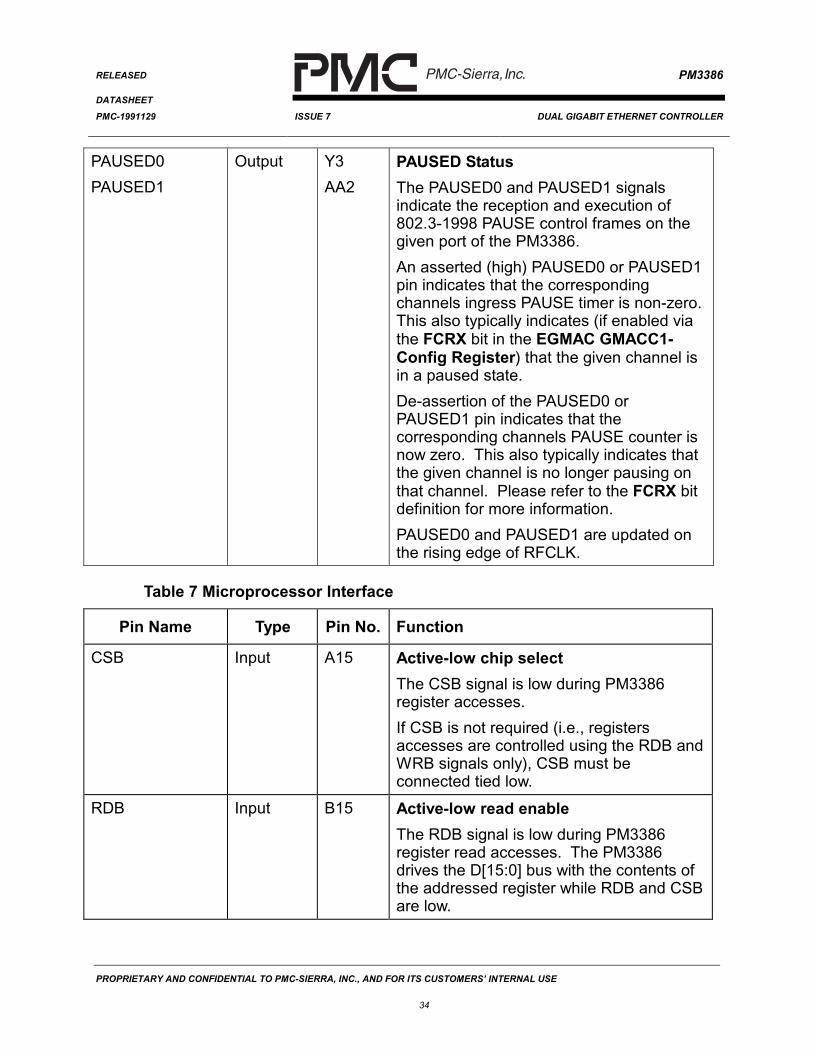
PAUSED0PAUSED1
Output Y3AA2
PAUSED StatusThe PAUSED0 and PAUSED1 signalsindicate the reception and execution of802.3-1998 PAUSE control frames on thegiven port of the PM3386.An asserted (high) PAUSED0 or PAUSED1pin indicates that the correspondingchannels ingress PAUSE timer is non-zero.This also typically indicates (if enabled viathe FCRX bit in the EGMAC GMACC1-Config Register) that the given channel isin a paused state.De-assertion of the PAUSED0 orPAUSED1 pin indicates that thecorresponding channels PAUSE counter isnow zero. This also typically indicates thatthe given channel is no longer pausing onthat channel. Please refer to the FCRX bitdefinition for more information.PAUSED0 and PAUSED1 are updated onthe rising edge of RFCLK.
Table 7 Microprocessor Interface
Pin Name Type Pin No. Function
CSB Input A15 Active-low chip selectThe CSB signal is low during PM3386register accesses.If CSB is not required (i.e., registersaccesses are controlled using the RDB andWRB signals only), CSB must beconnected tied low.
RDB Input B15 Active-low read enableThe RDB signal is low during PM3386register read accesses. The PM3386drives the D[15:0] bus with the contents ofthe addressed register while RDB and CSBare low.
PROPRIETARY AND CONFIDENTIAL TO PMC-SIERRA, INC., AND FOR ITS CUSTOMERS’ INTERNAL USE
35
Pin Name Type Pin No. Function
WRB Input C15 Active-low write strobeThe WRB signal is low during a PM3386register write accesses. The D[15:0] buscontents are clocked into the addressedregister on the rising WRB edge while CSBis low.
The bi-directional data busD[15:0] is used during PM3386 registerread and write accesses.
A[0]A[1]A[2]A[3]A[4]A[5]A[6]A[7]A[8]A[9]A[10]
Input C11A10B11A11C12B12A12C13B13B14C14
Address busA[10:0] selects specific registers duringPM3386 register accesses.
ALE InputInternalpull-up
A16 Address latch enableALE is active-high and latches the addressbus A[10:0] when low. When ALE is high,the internal address latches aretransparent. It allows the PM3386 tointerface to a multiplexed address/databus. ALE has an integral pull-up resistor.
PROPRIETARY AND CONFIDENTIAL TO PMC-SIERRA, INC., AND FOR ITS CUSTOMERS’ INTERNAL USE
36
Pin Name Type Pin No. Function
INTB OutputOpenDrain
B16 Active-low interruptINTB is set low when a PM3386 interruptsource is active and that source isunmasked. The PM3386 may be enabledto report many alarms or events viainterrupts.INTB is tri-stated when the interrupt isacknowledged via an appropriate registeraccess. INTB is an open drain output.
Table 8 - Device Miscellaneous
Name Type Pin No. Description
RSTB SchmittinputInternalpull-up
G3 Master ResetThis active low reset signal input providesan asynchronous reset to the device.RSTB is a Schmitt triggered input with aninternal pull-up resistor. When RSTB isforced low, all device registers are forced totheir default states.
PMD_SEL0PMD_SEL1
InputInternalpull-down
V24F25
Physical Medium SelectThese active high signals select betweenusing the on-board SERDES or externaltransceiver via the GMII pins.A low (tied to VSS) will select internalSERDES.A high (tied to VDDO) will select externaltransceiver via the GMII pins.These pins are required to be tied to VDDOor VSS prior to device power up.
PROPRIETARY AND CONFIDENTIAL TO PMC-SIERRA, INC., AND FOR ITS CUSTOMERS’ INTERNAL USE
37
Table 9 - JTAG Test Access Port (TAP) Signals
Name Type Pin No. Description
TCK Input C6 JTAG Test ClockThe JTAG test clock (TCK) signal providesclock timing for test operations that arecarried out using the IEEE P1149.1 testaccess port. TCK must be tied to VSS orVDDO when not in JTAG test.
TMS InputInternalpull-up
B5 JTAG Test Mode SelectTMS controls the test operations that arecarried out using the IEEE P1149.1 testaccess port. TMS is sampled on the risingedge of TCK. TMS has an internal pull upresistor.
TDI InputInternalpull-up
A4 JTAG test InputTDI carries test data into the PM3386 viathe IEEE P1149.1 test access port. TDI issampled on the rising edge of TCK. TDIhas an internal pull-up resistor
TDO Output D6 JTAG Test OutputTDO carries test data out of the PM3386via the IEEE P1149.1 test access port.TDO is updated on the falling edge of TCK.TDO is a tri-state output which is inactiveexcept when in the progress of shiftingboundary scan data out.
TRSTB SchmittInputInternalpull-up
C5 JTAG Test ResetTRSTB provides an asynchronous reset fortesting via the IEEE P1149.1 test accessport. TRSTB is a Schmitt triggered inputwith and internal put-up resistor.Note that when not being used for JTAGtesting the TRSTB pin must be connectedto the RSTB input for proper normal modeoperation.
PROPRIETARY AND CONFIDENTIAL TO PMC-SIERRA, INC., AND FOR ITS CUSTOMERS’ INTERNAL USE
42
Notes on Pin Description:
1. All PM3386 inputs and bi-directional signals present minimum capacitiveloading and operate at TTL logic levels except the inputs marked as Analogor PECL.
4. The PECL inputs and outputs should be terminated in a passive network andinterface at PECL levels as described in the Operations section.
5. It is mandatory that every ground pin (VSS) be connected to the printedcircuit board ground plane to ensure reliable device operation.
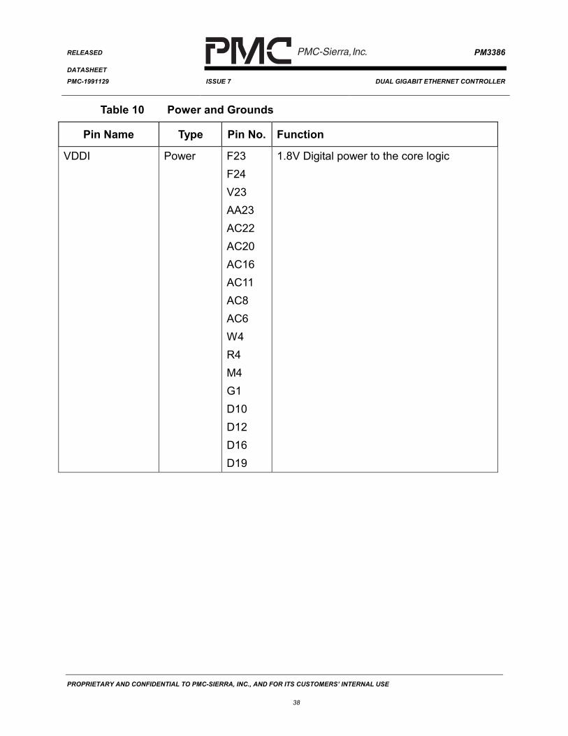
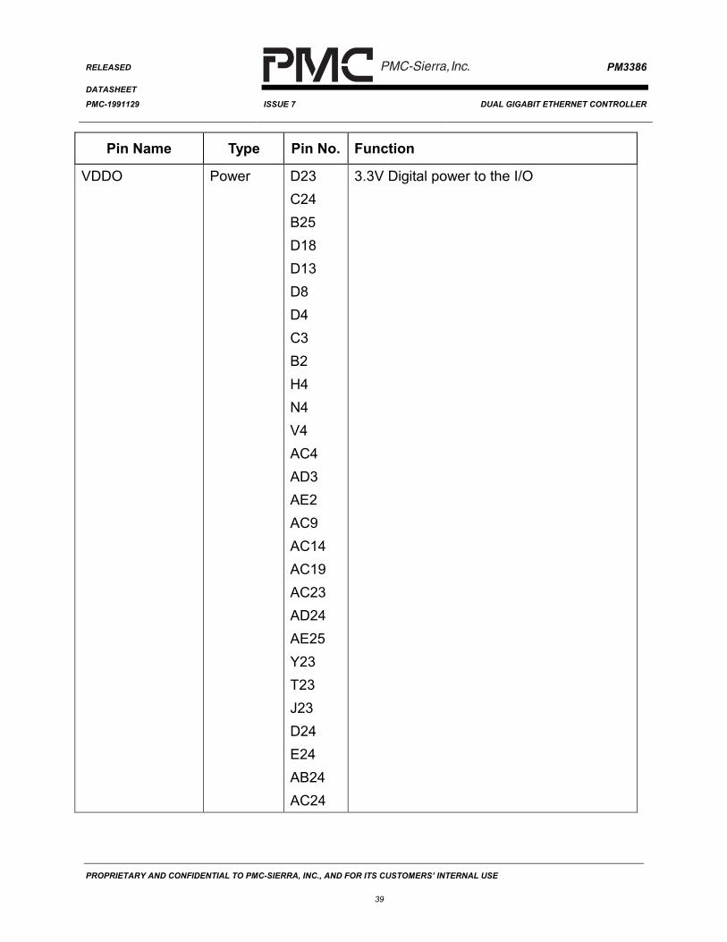
6. It is mandatory that every digital power pin (VDDI, VDDO, and VDDQ) beconnected to the printed circuit board power planes to ensure reliable deviceoperation.
7. All analog power pins can be sensitive to noise. They must be isolated fromthe digital power. Care must be taken to correctly decouple these pins.
8. It is mandatory that every analog power pin (AVDL, AVDH, and AVDQ) bede-coupled from but connected to the printed circuit board power planes toensure reliable device operation.
8. Due to ESD protection structures in the pads it is necessary to exercisecaution when powering a device up or down. ESD protection devices behaveas diodes between power supply pins and from I/O pins to power supply pins.Under extreme conditions it is possible to damage these ESD protectiondevices or trigger latch up. Please adhere to the recommended power supplysequencing as described in the Operation section of this document.
PROPRIETARY AND CONFIDENTIAL TO PMC-SIERRA, INC., AND FOR ITS CUSTOMERS’ INTERNAL USE
43
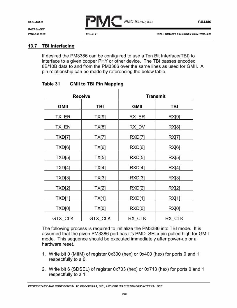
10 FUNCTIONAL DESCRIPTION
The PM3386 provides a high density and low power solution for implementingGigabit Ethernet connectivity. The PM3386 is a dual Gigabit Ethernet controllerwith integrated SERDES and GMAC functions connecting to a standard POS-PHY Level 3 system interface. The PM3386 accepts serial bit streams fromoptical transceiver devices or Gigabit Ethernet PHY devices and performs MediaAccess Control frame verification. Statistics are maintained and the frame isforwarded to internal FIFOs for the POS-PHY Level 3 interface. The PM3386may be connected to an upper layer device via the POS-PHY Level 3 interfacefor classification and forwarding.
The PM3386 is partitioned into the following major functional blocks. Theoperation of each block is described in more detail in subsequent sections.
• SERDES
• Enhanced Gigabit Media Access Control
• Ethernet Statistics
• Address Filtering
• POS-PHY Level 3 System Interface
• Microprocessor Interface
10.1 Serializer-Deserializer (SERDES)
The PM3386 has two internal serializer-deserializer transceivers. The SERDESis IEEE 802.3-1998 Gigabit Ethernet compatible supporting gigabit data transferflows. The SERDES is based on the X3T11 10 Bit specification. The PECL cellsused to implement the SERDES are capable of both 5V and 3.3V low voltagePECL operation as they can be AC coupled within the system design.
The transmitter section of the SERDES accepts 10-bit wide parallel data andserializes this data into a high-speed serial data stream. The parallel data is8B/10B encoded data. An internally generated reference clock is then multipliedto generate the 1250 MHz serial clock used to clock the encoded data out thehigh-speed output at a rate of 1250 Mbit/s. The high-speed outputs are capableof interfacing directly to a separate fiber optic module for optical transmission.
PROPRIETARY AND CONFIDENTIAL TO PMC-SIERRA, INC., AND FOR ITS CUSTOMERS’ INTERNAL USE
44
The receiver section accepts a serial electrical data stream at 1250 Mbit/s andrecovers the original 10-bit wide parallel data. The receiver Clock Recovery Unit(CRU) locks onto the incoming serial signal and facilitates the recovery of thehigh-speed serial data. The serial data is converted back into 10-bit paralleldata, recognizing the 8B/10B comma character to establish byte alignment. Therecovered parallel data is presented to the EGMAC.
10.2 Enhanced Gigabit Media Access Control (EGMAC)
10.2.1 EGMAC General
The PM3386 integrates standard IEEE 802.3-1998 Gigabit Ethernet MediaAccess Control interfaces for connection to internal serializer-deserializers(SERDES) or external transceivers using Gigabit Media Independent Interface(GMII) pins on each gigabit Ethernet port. The dual ports of the PM3386 arecapable of operation in either SERDES or GMII mode. The ports can beconfigured to operate independently from each other using the PMD_SEL0 andPMD_SEL1 pins.
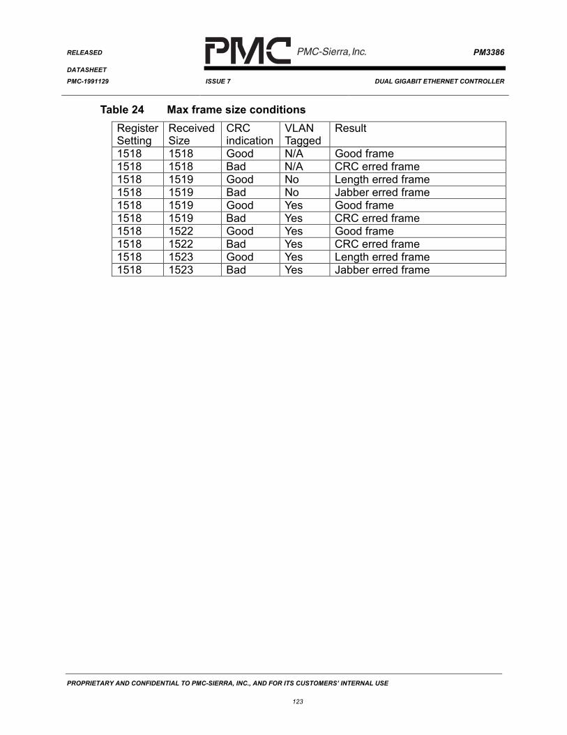
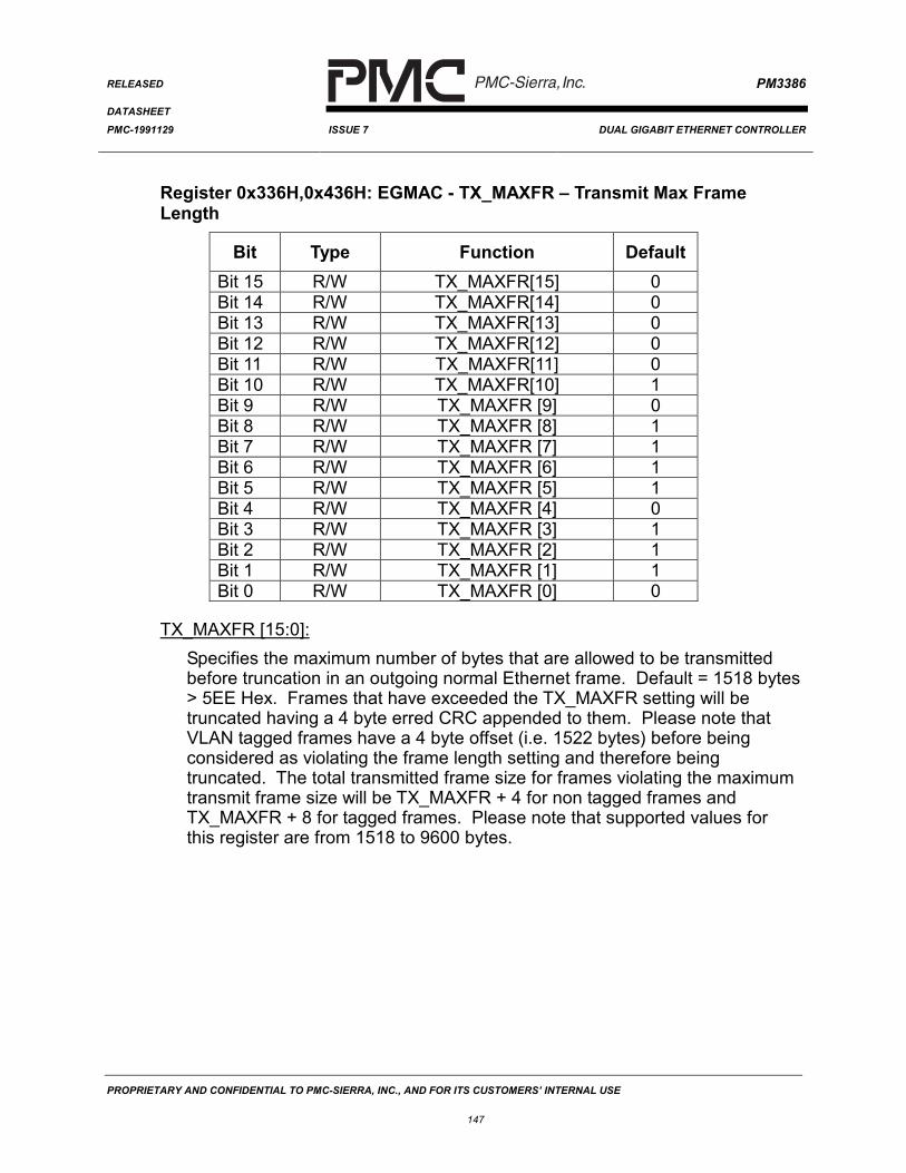
The EGMAC is capable of supporting normal Ethernet frame sizes of 1518bytes, VLAN tagged frame sizes of 1522 bytes, and Jumbo frames sizes up to9.6k bytes. The Transmit Max Frame Length and the Receive Max FrameLength registers contain the values associate with maximum accepted Ethernetframe sizes. By default these registers contain a value of 1518 bytes. Thisallows for normal frame sizes as well as 1522 VLAN tagged frames to beaccepted. The EGMAC will base all frame length calculations and statistics off ofthese registers. The EGMAC takes into account the VLAN tagging of frames toensure their proper representation in the statistics gathering process. Note that itis possible to program the ingress and egress maximum frame sizes separately.
10.2.2 EGMAC Egress Direction
In the egress direction packet data from the PL3EP is presented to the EGMACsynchronizing transmit FIFO. The EGMAC/PL3EP interface is a push styleinterface. If packet data is available for transmit the PL3EP will push (transfer)data to the EGMAC. The PL3EP will notify the EGMAC of the start and end ofpackets by using simple end of packet and start of packet indications. ThePL3EP will also present to the EGMAC an error signal that is asserted when anerror condition is observed on the POS-PHY bus or if an internal error isencountered in the egress data path.
The EGMAC has an upper bound of 9.6k bytes on the size of egress frames.The egress direction of the EGMAC can accept packets of a minimum size of 14bytes. Egress packets sent to the EGMAC that are of the minimum 14 bytes but
PROPRIETARY AND CONFIDENTIAL TO PMC-SIERRA, INC., AND FOR ITS CUSTOMERS’ INTERNAL USE
45
are less than the minimum 64 byte frame length required by 802.3-1998 havethe programmed option to be padded appropriately to 64 bytes (68 bytes forVLAN tagged frames) and optionally have the associated 32 bit CRC appendedto the frame prior to transmit. The user may also elect to program the EGMAC toinsert the Frame Check Sequence (FCS) field.
In the case that the link device disregards the flow control information providedby DTPA0, DTPA1, STPA, or PTPA and continues to write to the PM3386 in anattempt to overflow the egress FIFO the PM3386 will truncate the current packetwhen the FIFO becomes full. At this time the PM3386 will wait until a minimumpacket can be accepted and then resume data transfer.
In the event that the link device can not deliver the data fast enough to thePM3386, placing the PM3386 in a case of FIFO underrun, the current packet willbe truncated sending all bytes currently available and then the PM3386 will re-sync to TSOP. In all error cases the CRC-32 that is kept over the packet will beinvalidated and appended to the frame as it is transmitted thereby signaling anerror.
Following each frame transmission the EGMAC provides a statistical vector tothe MSTAT block that updates statistic collection counters maintained in systemvisible registers. Please refer to the MSTAT functional description and Registersection of this document for a full list of port statistics.
10.2.3 EGMAC Ingress Direction
In the ingress direction the SERDES or GMII presents receive physical packet tothe EGMAC. The EGMAC scans the preamble looking for the Start FrameDelimiter (SFD). By default the preamble and SFD are stripped converting thephysical packet to a frame. The EGMAC will then compare the destinationaddress in the frame to the address filtering logic for the given port. If enabledthe address filtering logic may be programmed to accept or reject incomingframes. The EGMAC is also programmable to accept all frames regardless ofvalidity.
The EGMAC supports ingress frame sizes of up to 9.6k bytes. The EGMACinterfaces to the PL3IP using a simple push style interface. The EGMAC signalsstart of frame and end of frame while transferring data information to the PL3IP.
There are two decision points at which the frame forwarding and filteringdecisions are made. The first decision point is at the beginning of the ingressframe. At this point and once the SA, DA, and the possible VID fields arerecognized the frame may be filtered based on the address filter logic describedlater. If the frame is to be forwarded the incoming data will be written to the
PROPRIETARY AND CONFIDENTIAL TO PMC-SIERRA, INC., AND FOR ITS CUSTOMERS’ INTERNAL USE
46
EGMAC ingress FIFO in preparation for frame transfer. If the frame is to befiltered the frame will not be written to the EGMAC FIFO and the EGMAC will re-sync to the next incoming ingress frame.
The second decision point is at the end of the frame. The EGMAC will performframe integrity checks such as length and CRC. If the frame violates theseintegrity checks the frame will need to be discarded. Discarding a frame can bedone in two possible ways. The cases are described below.
1. If the number of bytes that have been written to the EGMAC ingressFIFO are less than the programmed value within the EGMAC ReceiveFIFO Forwarding Threshold register, the frame in its entirety is storedwithin the FIFO, and will therefore be dropped within the EGMAC. TheEGMAC will flush this frame from the FIFO and resume reception ofingress traffic on the next start of frame indication.
2. If the number of bytes that have been written to the EGMAC ingressFIFO are greater than the programmed value within the EGMAC ReceiveFIFO Forwarding Threshold register the frame will have started drainingfrom the FIFO and therefore can not be dropped within the PM3386. Inthis case the frame will be marked as bad by assertion of the RX_ERR biton the EGMAC PL3IP interface. This indication is carried to the POS-PHY Level 3 interface and will cause the assertion of the RERR bit on thelast byte transfer of the packet.
As mentioned above ingress frames are held in the receive FIFO within theEGMAC until the byte count exceeds the forwarding threshold programmed inthe EGMAC Receive FIFO Forwarding Threshold register or until End OfFrame (EOF). Frames that contain errors and are greater than the programmedvalue within the EGMAC Receive FIFO Forwarding Threshold register will bemarked as erred by the PM3386 but will not be discarded within the PM3386.
The EGMAC will distinguish between unicast, broadcast, and multicast frames.The EGMAC can be programmed to forwarded or filter frames based on unicast,broadcast, or multicast type frames.
10.2.4 EGMAC Flow Control - MAC Control Sublayer
The PM3386 provides loss-less frame flow control for frame sizes up to 9.6kbytes over 1000BASE TX, 1000BASE SX, and 1000BASE LX implementations.
The EGMAC interface contains the MAC Control Sublayer which adheres toIEEE 802.3-1998 and provides support for Control frames. The EGMACperforms the functions out lined in IEEE 802.3-1998 Clause 31 “MAC Control”and Annexes 31A and 31B. Clause 31 introduces the optional MAC Control
PROPRIETARY AND CONFIDENTIAL TO PMC-SIERRA, INC., AND FOR ITS CUSTOMERS’ INTERNAL USE
47
sublayer to the popular layer stack. This sublayer provides for real-time controland manipulation of the MAC operation. The clause defines MAC control framesdistinguishable by their unique Length/Type field identifier.
The EGMAC supports Annex 31A opcode PAUSE by implementing Annex31B’sframe based flow control scheme which utilizes PAUSE Control frames. Thepurpose of flow control is to slow down the aggregate rate of frames that theother end of a link is sending. Finite FIFO depths have a tendency to overflowwhen line-rate frames are being received and the upper layer device cannotkeep up. Thus to prevent the overflow of the FIFOs, flow control is used. A MACControl client wishing to inhibit transmission of data frames from the PM3386generates a PAUSE Control frame which contains the reserved multicastaddress (01-80-C2-00-00-01), the Control frame type field 88-08, the PAUSEopcode, 00-01, and the pauseTimer, a 16-bit value expressed in pause quanta of512 bit times. When the EGMAC receives a PAUSE Control frame, it loads thePause Timer with the value sent in the pauseTime filed. If pauseTime is non-zero and the FCRX bit within the EGMAC GMACC1-Config Register isasserted, the EGMAC will pause from transmitting frames and will wait forpauseTime number of slot times before resuming operation. If, however, thepauseTime value is equal to zero, the EGMAC is allowed to resume transmittingdata frames. At any time if the EGMAC is receiving PAUSE control frames theEGMAC will assert the PAUSED0 or PAUSED1 status pins. These pins will beheld asserted until the EGMAC pauseTime counts down to zero and the EGMACresumes transmitting data frames. It is possible depending on the systemrequirements to allow ingress PAUSE Control frames to be processed or notprocessed at the EGMAC layer (see FCRX bit) and PAUSE Control frames to bedropped at the EGMAC layer or passed to the upper layer device(seePASS_CTRL bit).
If for any reason the upstream device needs to stop incoming frames, it canaccomplish this by four different ways. First, the upper layer device can send802.3-1998 PAUSE Control frames of its own. Second, the upper layer devicecan assert the PAUSE0 or PAUSE1 pins on the device to have the EGMACautomatically send PAUSE Control frames. Third, the system processor caninitiate PAUSE operation via configuration registers in the EGMAC. Fourth, thelink device can de-assert RENB and cause the FIFO fill levels in the PL3IP blockto fill and start automatic flow control. Note that even though the EGMAC can besending egress PAUSE Control frames the ingress channel will still beoperational with the exception of normal blocking of the POS-PHY L3 data-pathfrom the link level. Please refer to the Operations section under PAUSE FlowControl for programming options.
At the end of a PAUSE operation the PM3386 will send a PAUSE frame with anull Pause Timer value allowing quick PAUSE off signaling to downstreamdevices.
PROPRIETARY AND CONFIDENTIAL TO PMC-SIERRA, INC., AND FOR ITS CUSTOMERS’ INTERNAL USE
48
10.2.5 EGMAC Auto-Negotiation
The EGMAC implements Clause 37 of the IEEE 802.3-1998 Standard, Auto-Negotiation function, type 1000BASE-X. The Auto-Negotiation for 1000BASE-Xfunction provides the means to exchange information between two devices thatshare a link segment allowing management the ability to configure both devicesin such a way that takes maximum advantage of their capabilities. After a resetoccurs the EGMAC senses whether or not Auto-Negotiation is enabled. If so theEGMAC will start Auto-Negotiation exactly following the state diagram as outlinedin 802.3-1998 Clause 37. Base page Auto-Negotiation is therefore completelytaken care of by the EGMAC.
Above base page Auto-Negotiation, the EGMAC communicates between thehost processor and an external MII physical device by means of a two wireinterface. The EGMAC block produces the clock (MDC) and the general MII I/Opin MDIO. The host controls the EGMAC MII via the MII management registers.
10.2.6 EGMAC Address Filter Logic
The EGMAC provides a rich set of address filtering options. The hostmicroprocessor has complete programmable access to all filtering features.
The EGMAC can perform 8 separate exact-match MAC/VID unicast filteroperations. Each unicast filter will perform an exact match on either the DA orthe SA, and an optional exact match on the VID. If enabled, each unicast filterchannel can be programmed to indicate ACCEPT or DISCARD upon match.Each unicast filter channel can be enabled separately.
The EGMAC also includes a 64-bin hash-based multicast filter. This hash-basedfilter utilizes 6-bits of the CRC-32 output taken over the MAC DA to provide thestandard imperfect multicast filtering capability. The multicast filter output will beasserted only if the IEEE Group/Functional bit is set in the DA of the frame (Mostsignificant bit of the least significant byte of the MAC DA). If enabled, the filteroutput will indicate ACCEPT only. If not enabled, it will indicate nothing.
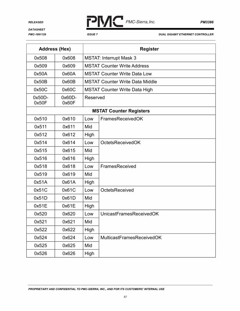
10.3 Management Statistics (MSTAT)
The MSTAT block is used to accumulate Ethernet specific counts used forsupporting management agents such RMON, SNMP, and Etherlike interfaces.The MSTAT provides counter width support for compliance with 802.3-1998
PROPRIETARY AND CONFIDENTIAL TO PMC-SIERRA, INC., AND FOR ITS CUSTOMERS’ INTERNAL USE
49
rollover requirements of 58 minutes. The MSTAT supports full system probingwith counter snapshotting via shadow registers. Incorporated into the MSTATblock is a fully programmable interrupt array enabling per counter rollovermonitoring with interrupt reporting.
10.4 POS-PHY Level 3 Physical Layer Interface
10.4.1 POS-PHY Level 3 General
The PM3386 can connect to a single upper level device through a POS-PHYLevel 3 Interface. The POS-PHY Level 3 interface is a 32-bits wide interfacewith a clock rate of 104 MHz. POS-PHY Level 3 was developed with thecooperation of the SATURN Development Group to cover all application bit ratesup to and including 3.2 Gbit/s. The POS-PHY Level 3 specification defines therequirements for interoperation between devices such as the multi-PHY PM3386and a single Link Layer device. Each channel within the PM3386 contains a 64kbyte ingress and 16k byte egress POS-PHY latency FIFO.
As a POS-PHY slave device, hence in the ingress or receive direction, thePM3386 outputs received packets to the upper layer device whenever data isavailable. The interface accepts a read clock (RFCLK) and read enable signal(RENB) when data is read from the ingress FIFO (using the rising edge of theRFCLK). The start of packet (RSOP) marks the first byte of received packet dataon the RDAT[31:0] bus. The RPRTY signal reports parity on the RDAT[31:0]bus. Parity defaults to odd but may be programmed for even parity. The end ofa packet is indicated by the REOP signal. The RERR signal is provided toindicate that an error in a received packet has occurred. The RVAL signal isused to indicate when RSOP, REOP, RERR, and RDAT[31:0] are valid. RSXindicates the start of transfer and marks the clock cycle where the in-bandchannel address is given on the RDAT[31:0] bus.
In the event that the upper level device cannot accept data it can de-assertRENB. At this point the specific port’s POS-PHY interface ingress 64k byte FIFOwill start to fill up. When the FIFO exceeds the programmed high water markflow control threshold the ingress FIFO will assert an indication to the EGMAC tostart PAUSE flow control. The ingress POS-PHY FIFO will continue to keep theflow control signal high until the number of entries in the FIFO have decreased tothe programmed low water mark flow control threshold level.
PROPRIETARY AND CONFIDENTIAL TO PMC-SIERRA, INC., AND FOR ITS CUSTOMERS’ INTERNAL USE
50
In the event that the link layer device does not re-assert RENB to continue thedata flow the PM3386 will buffer the incoming frames from the line side interfaceuntil all the buffer facilities within the PM3386 are exhausted. At this time thePM3386 will no longer accept data from the line side. All data bits will bedropped at the line interface until resources within the PM3386 becomeavailable. At this time the PM3386 will re-sync to physical packet and continuereception. In the event that the PM3386 truncates a frame because of resourceexhaustion the frame will be marked as erred by asserting the RERR bit on thelast interface transaction for the packet transfer as specified by the PL3 busprotocol.
The POS-PHY ingress FIFO will absorb in-flight frames when the PM3386 isplaced into a PAUSE flow control state from the upper level device. The FIFOwill accept a number of maximum size 9.6k byte frames without loss.
The scheduling of packets through the ingress POS-PHY interface is controlledvia a simple round robin approach that fairly switches between both GigabitEthernet channels. The POS-PHY bursts packets across the interface usingprogrammable burst sizes.
The POS-PHY Level 3 compliant interface consists of a write clock (TFCLK), awrite enable signal (TENB), the start of packet (TSOP) indication, the end ofpacket (TEOP) indication, erred packet (TERR) indication, and the parity bit(TPRTY).
The PM3386 supports all three POS-PHY Level 3 egress status modes. TheSTPA signal reports the selected egress FIFO’s fill status. The PTPA signalshows the FIFO fill status for the polled channel. The DTPA[1:0] signal pinsshow the direct FIFO fill status on a per-channel basis. The TSX signal indicateswhen the in-band channel selection is given on the TDAT[7:0] pins. This is doneat the beginning of each transfer sequence. If the in-band address does notequal 0 or 1 subsequent data transfers on the TENB bus will be dropped.
The TMOD[1:0] signal is provided to indicate whether 1, 2, 3, or 4 bytes are validon the final word transfer of the packet(TEOP is asserted). A packet may beaborted by asserting the TERR signal at the end of the packet.
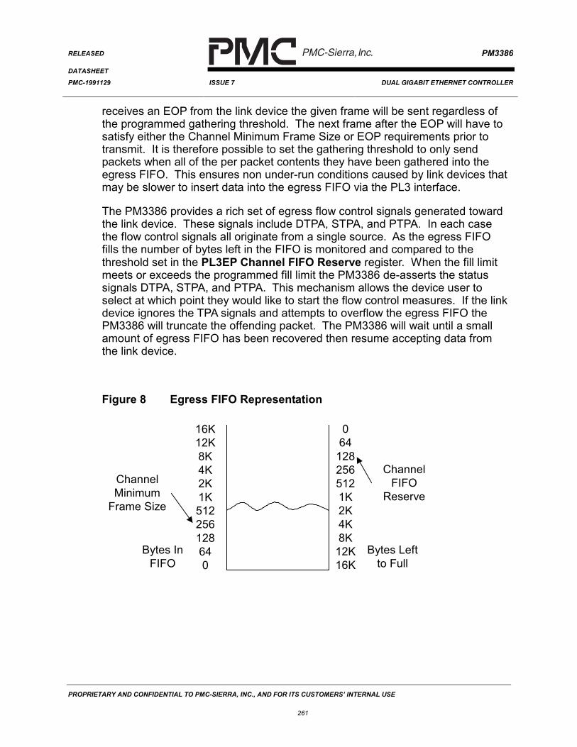
In the egress direction the PM3386 collects packets into the PM3386 egressFIFO and delays data transfer to the PM3386 EGMAC for transmission until thenumber of bytes gathered are equal to or greater than the PL3EP ChannelMinimum Frame Size register or until end of packet (via TEOP) is signaled.Each packet must satisfy one of the two forwarding conditions prior to
PROPRIETARY AND CONFIDENTIAL TO PMC-SIERRA, INC., AND FOR ITS CUSTOMERS’ INTERNAL USE
51
transmission. This allows for programmable MAC underrun protectiondepending upon the application.
10.5 Microprocessor Interface
The PM3386 uses a simple 16 bit multiplexed or non-multiplexed microprocessorinterface that is commonly found on PMC-Sierra devices.
The PM3386 supports complete accessibility to internal resources from the hostmicroprocessor. This allows the host to read and write all host accessibleregisters and chip data structures.
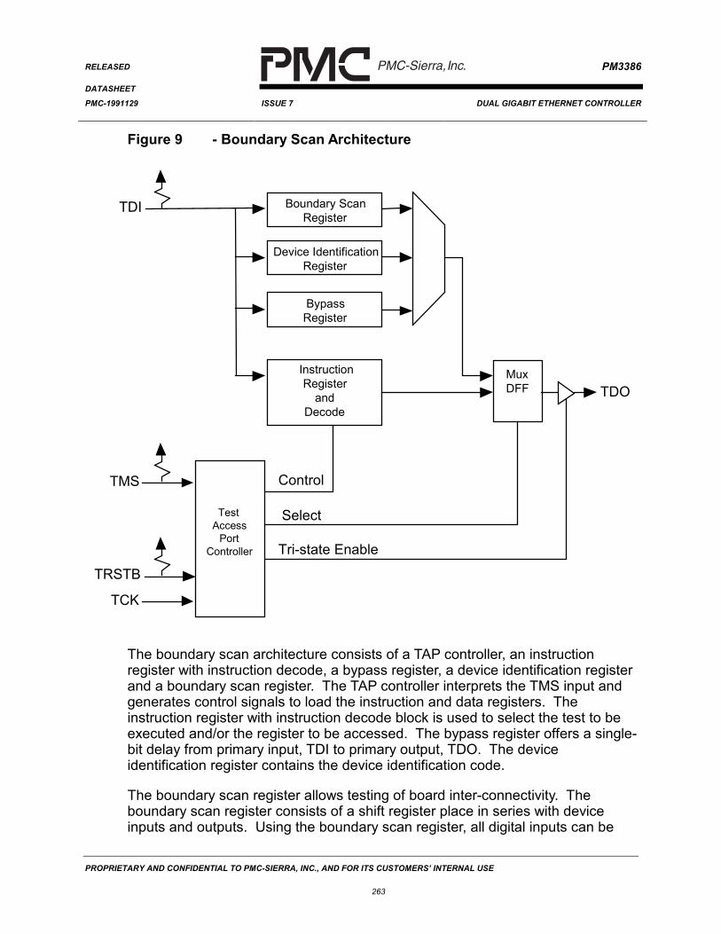
10.6 JTAG Test Access Port Interface
The JTAG Test Access Port block provides JTAG support for boundary scan.The standard JTAG EXTEST, SAMPLE, BYPASS, IDCODE and STCTESTinstructions are supported. The PM3386 identification code is 033860CDhexadecimal.
PROPRIETARY AND CONFIDENTIAL TO PMC-SIERRA, INC., AND FOR ITS CUSTOMERS’ INTERNAL USE
52
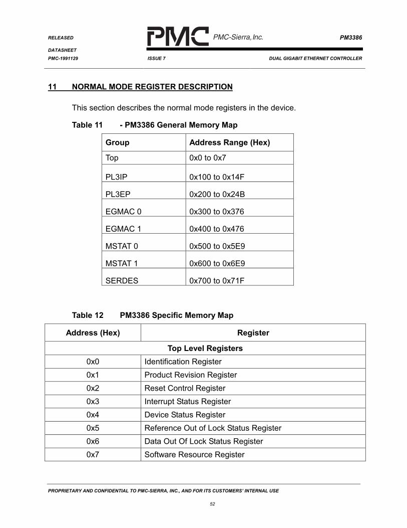
11 NORMAL MODE REGISTER DESCRIPTION
This section describes the normal mode registers in the device.
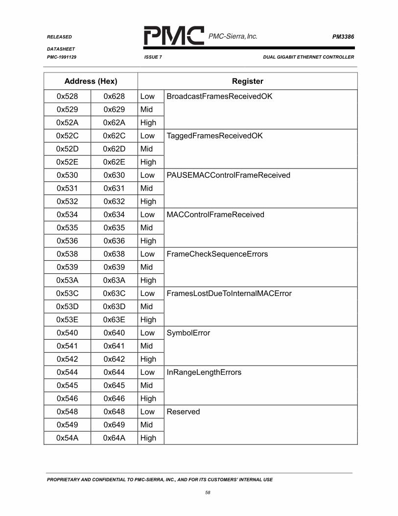
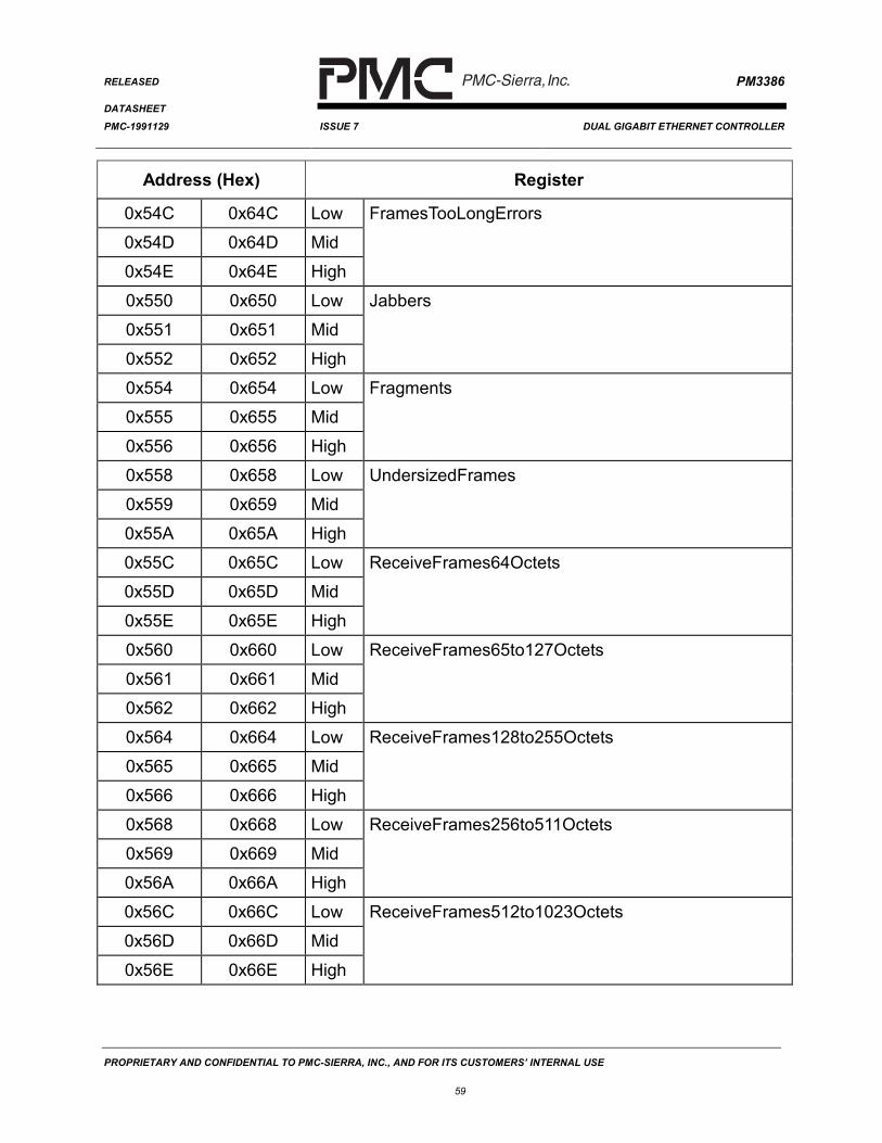
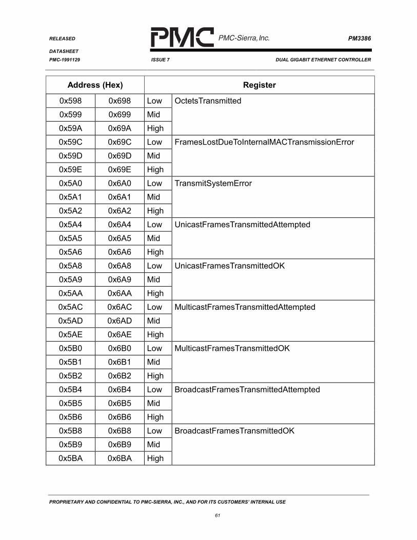
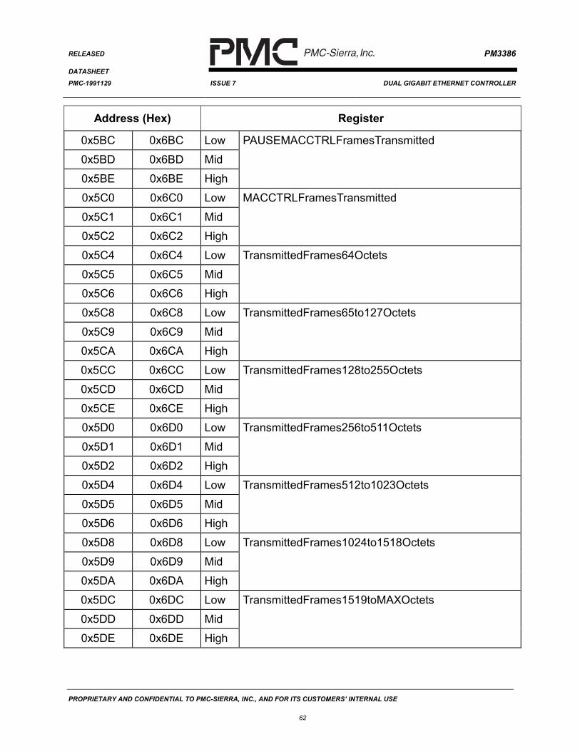
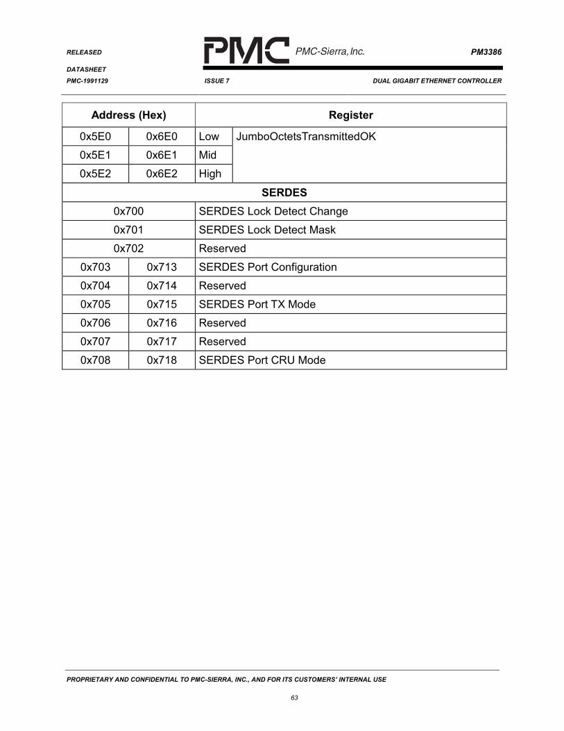
Table 11 - PM3386 General Memory Map
Group Address Range (Hex)
Top 0x0 to 0x7
PL3IP 0x100 to 0x14F
PL3EP 0x200 to 0x24B
EGMAC 0 0x300 to 0x376
EGMAC 1 0x400 to 0x476
MSTAT 0 0x500 to 0x5E9
MSTAT 1 0x600 to 0x6E9
SERDES 0x700 to 0x71F
Table 12 PM3386 Specific Memory Map
Address (Hex) Register
Top Level Registers0x0 Identification Register0x1 Product Revision Register0x2 Reset Control Register0x3 Interrupt Status Register0x4 Device Status Register0x5 Reference Out of Lock Status Register0x6 Data Out Of Lock Status Register0x7 Software Resource Register
PROPRIETARY AND CONFIDENTIAL TO PMC-SIERRA, INC., AND FOR ITS CUSTOMERS’ INTERNAL USE
55
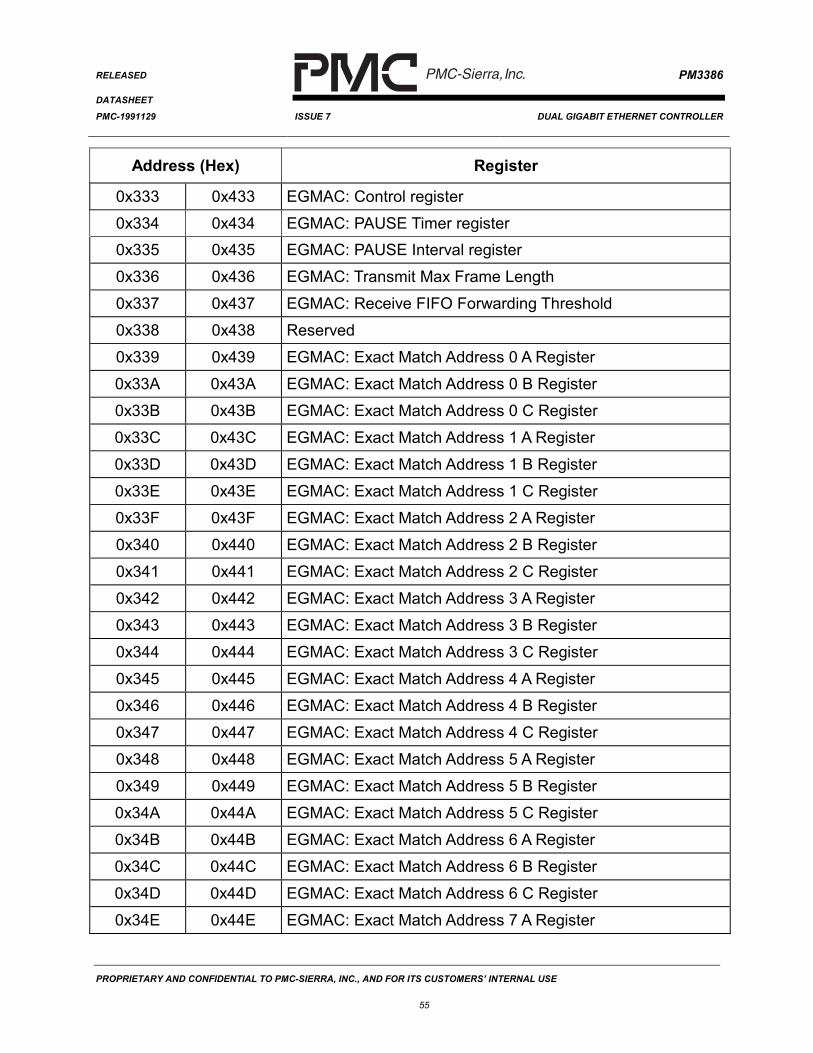
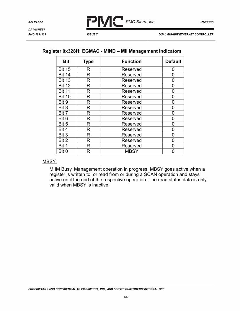
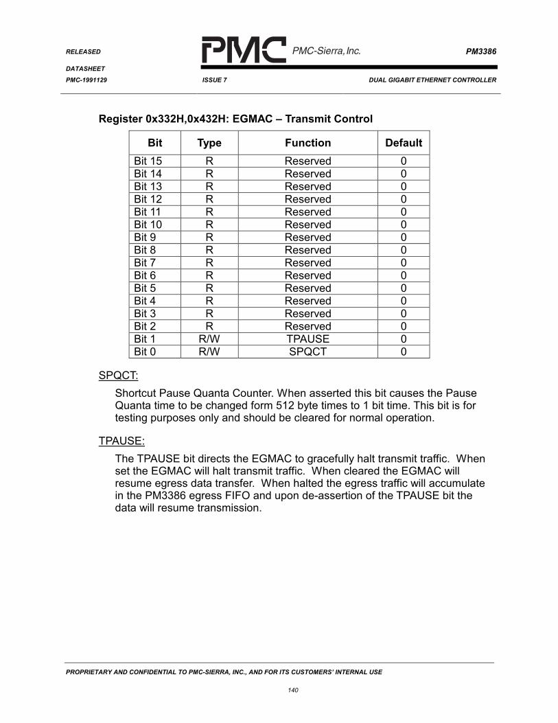
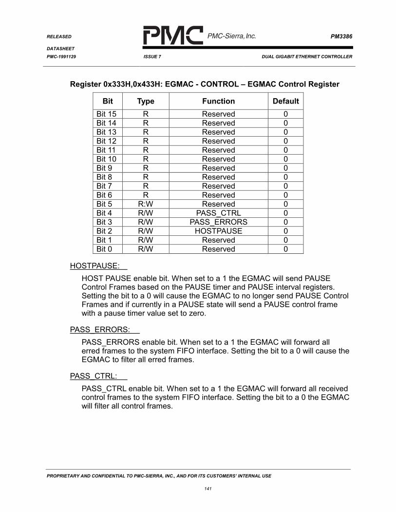
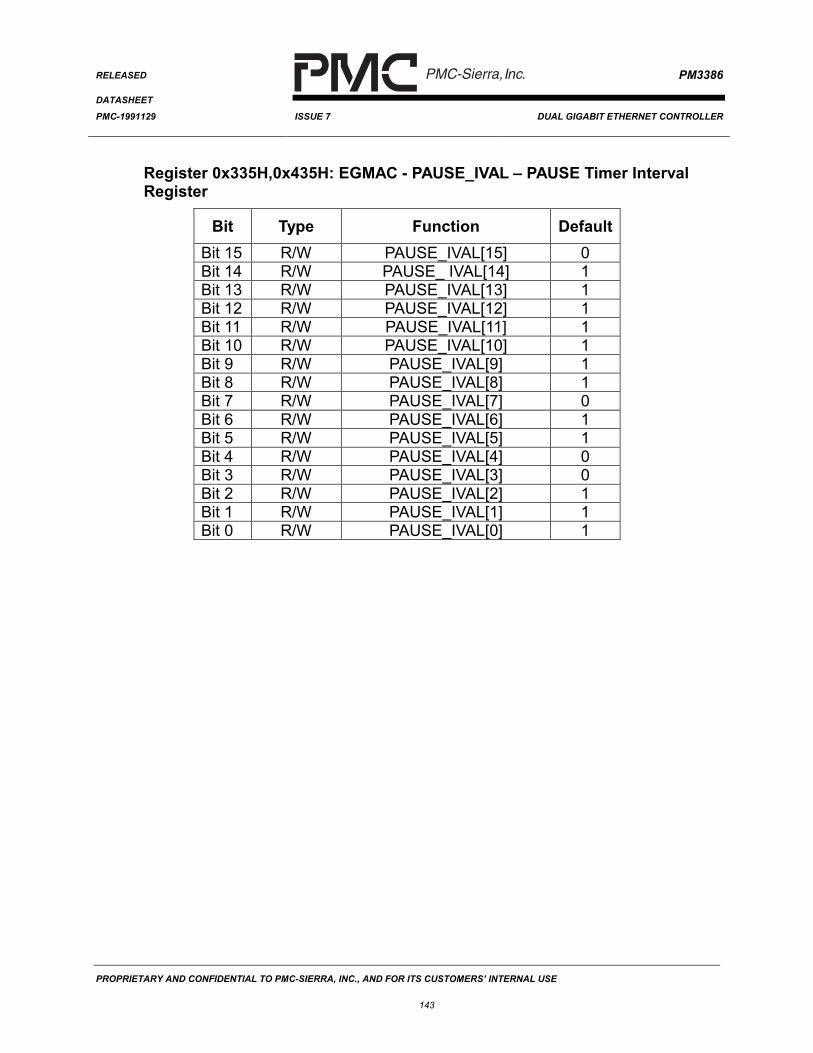
Address (Hex) Register
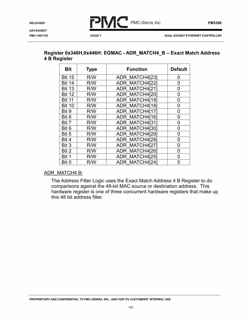
0x333 0x433 EGMAC: Control register0x334 0x434 EGMAC: PAUSE Timer register0x335 0x435 EGMAC: PAUSE Interval register0x336 0x436 EGMAC: Transmit Max Frame Length0x337 0x437 EGMAC: Receive FIFO Forwarding Threshold0x338 0x438 Reserved0x339 0x439 EGMAC: Exact Match Address 0 A Register0x33A 0x43A EGMAC: Exact Match Address 0 B Register0x33B 0x43B EGMAC: Exact Match Address 0 C Register0x33C 0x43C EGMAC: Exact Match Address 1 A Register0x33D 0x43D EGMAC: Exact Match Address 1 B Register0x33E 0x43E EGMAC: Exact Match Address 1 C Register0x33F 0x43F EGMAC: Exact Match Address 2 A Register0x340 0x440 EGMAC: Exact Match Address 2 B Register0x341 0x441 EGMAC: Exact Match Address 2 C Register0x342 0x442 EGMAC: Exact Match Address 3 A Register0x343 0x443 EGMAC: Exact Match Address 3 B Register0x344 0x444 EGMAC: Exact Match Address 3 C Register0x345 0x445 EGMAC: Exact Match Address 4 A Register0x346 0x446 EGMAC: Exact Match Address 4 B Register0x347 0x447 EGMAC: Exact Match Address 4 C Register0x348 0x448 EGMAC: Exact Match Address 5 A Register0x349 0x449 EGMAC: Exact Match Address 5 B Register0x34A 0x44A EGMAC: Exact Match Address 5 C Register0x34B 0x44B EGMAC: Exact Match Address 6 A Register0x34C 0x44C EGMAC: Exact Match Address 6 B Register0x34D 0x44D EGMAC: Exact Match Address 6 C Register0x34E 0x44E EGMAC: Exact Match Address 7 A Register
PROPRIETARY AND CONFIDENTIAL TO PMC-SIERRA, INC., AND FOR ITS CUSTOMERS’ INTERNAL USE
56
Address (Hex) Register
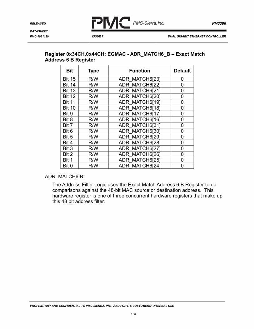
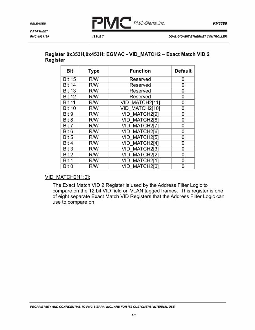
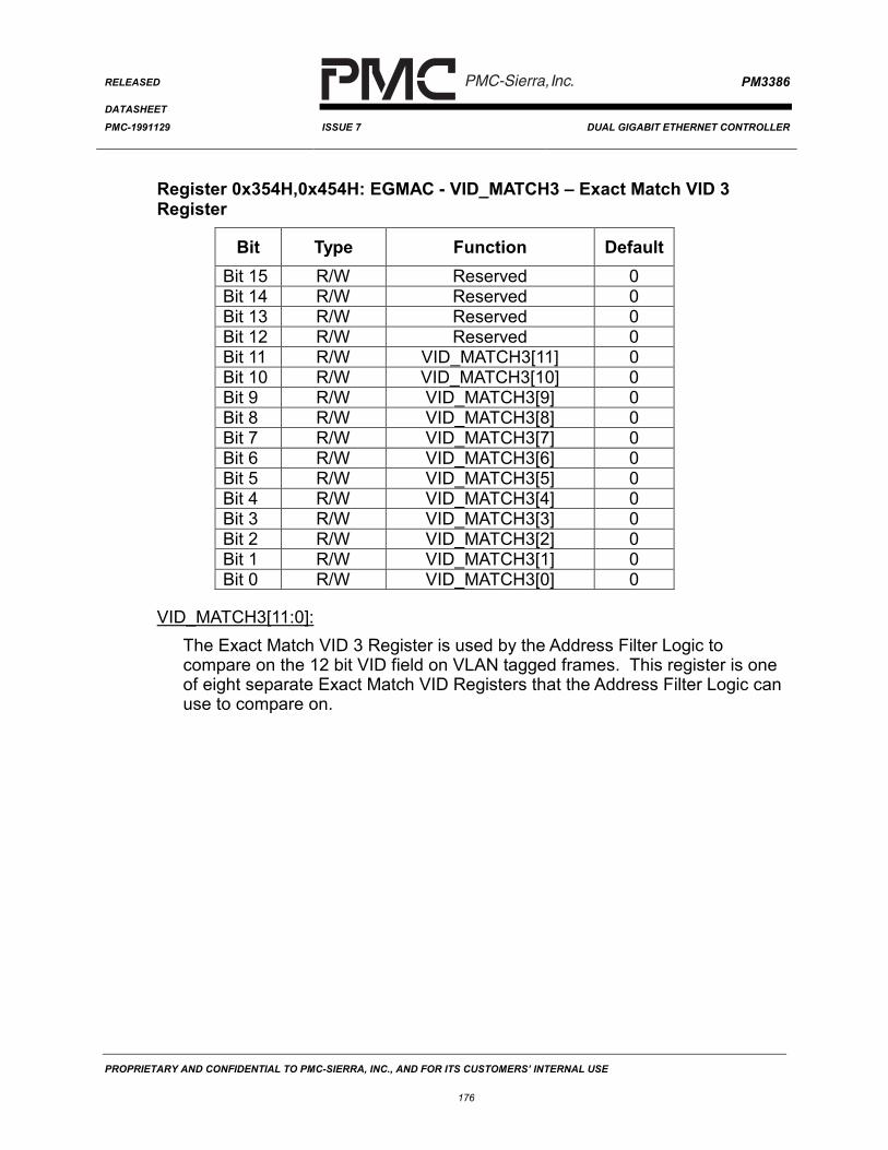
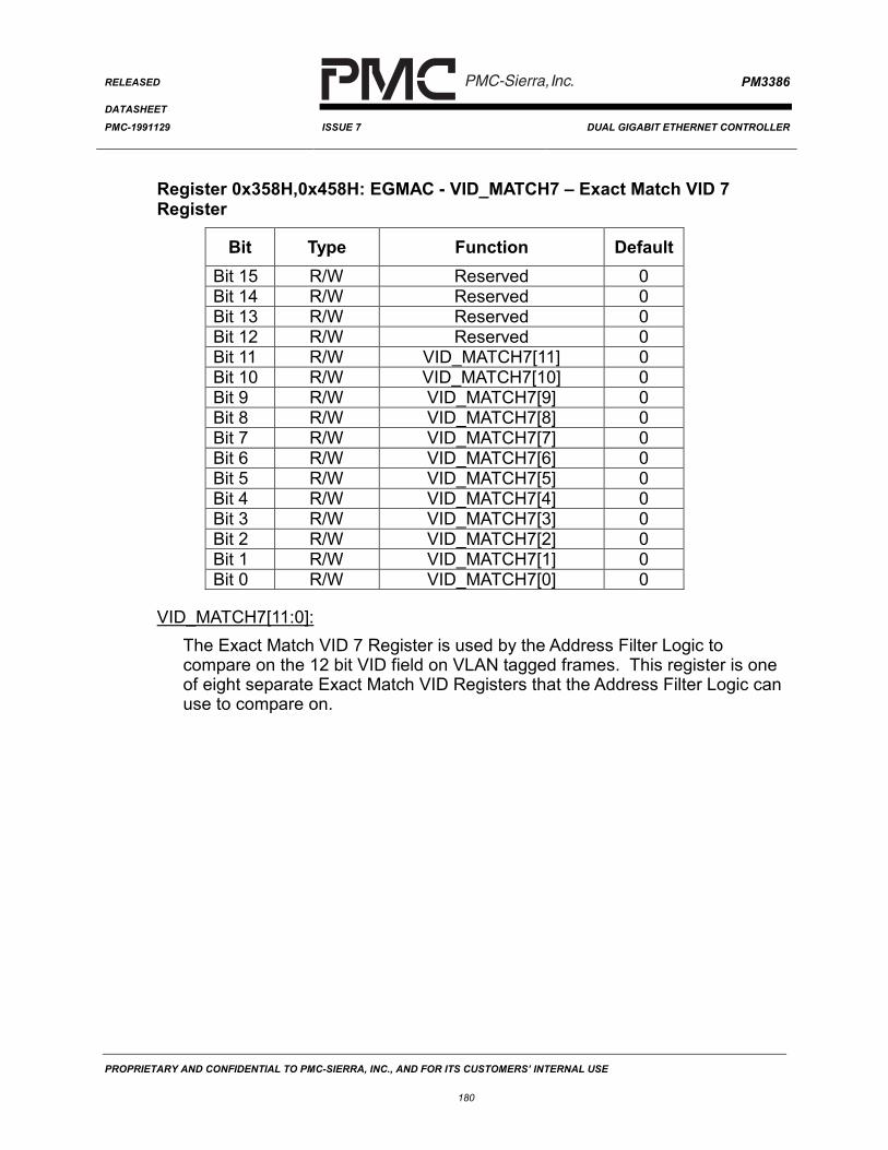
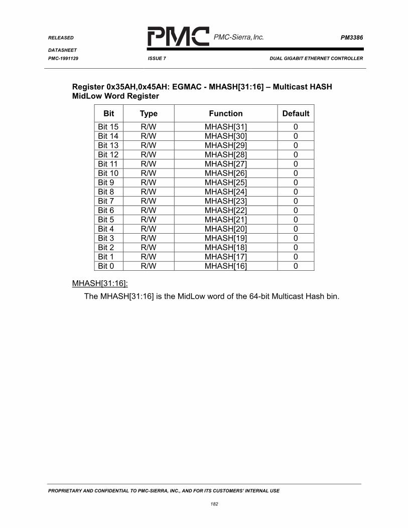
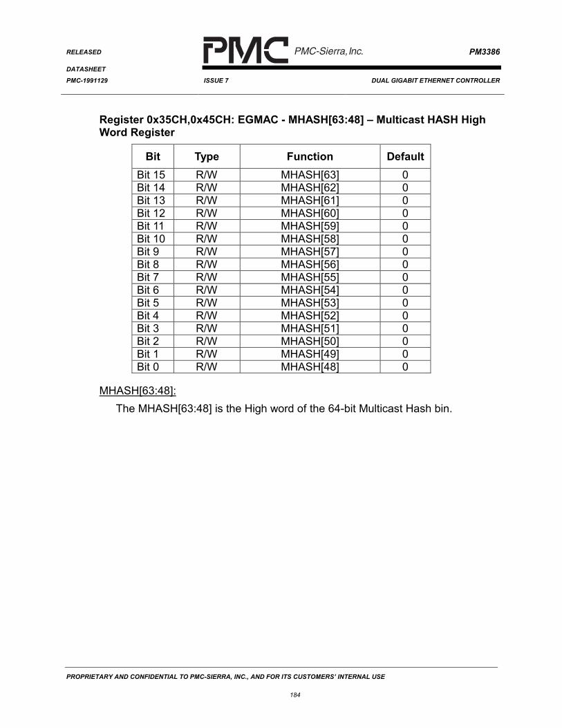
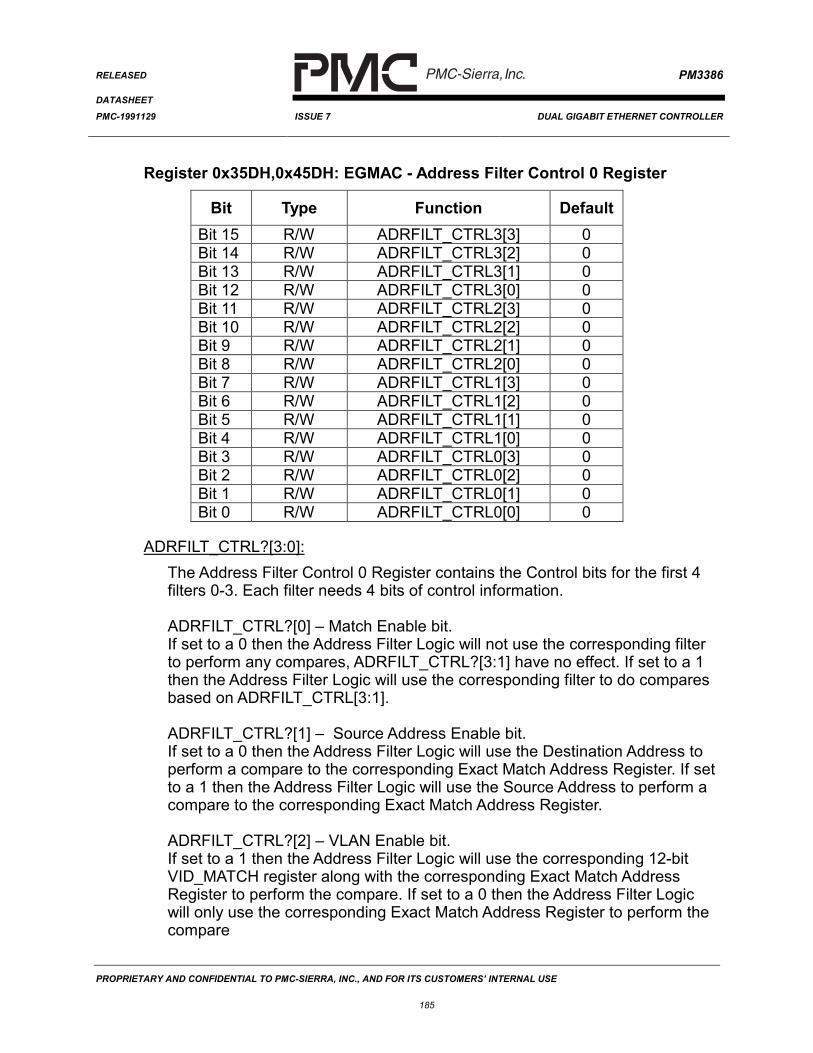
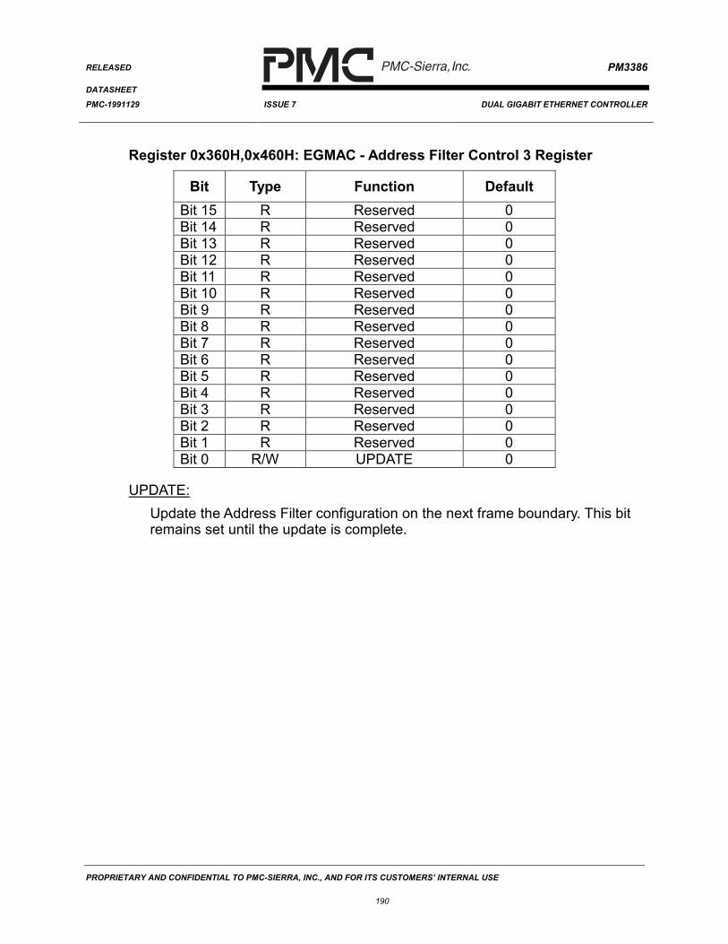
0x34F 0x44F EGMAC: Exact Match Address 7 B Register0x350 0x450 EGMAC: Exact Match Address 7 C Register0x351 0x451 EGMAC: Exact Match VID 0 Register0x352 0x452 EGMAC: Exact Match VID 1 Register0x353 0x453 EGMAC: Exact Match VID 2 Register0x354 0x454 EGMAC: Exact Match VID 3 Register0x355 0x455 EGMAC: Exact Match VID 4 Register0x356 0x456 EGMAC: Exact Match VID 5 Register0x357 0x457 EGMAC: Exact Match VID 6 Register0x358 0x458 EGMAC: Exact Match VID 7 Register0x359 0x459 EGMAC: Multicast Hash Low Word Register0x35A 0x45A EGMAC: Multicast Hash MidLow Word Register0x35B 0x45B EGMAC: Multicast Hash MidHigh Word Register0x35C 0x45C EGMAC: Multicast Hash High Word Register0x35D 0x45D EGMAC: Address Filter Control 0 Register0x35E 0x45E EGMAC: Address Filter Control 1 Register0x35F 0x45F EGMAC: Address Filter Control 2 Register0x360 0x460 EGMAC: Address Filter Control 3 Register
PROPRIETARY AND CONFIDENTIAL TO PMC-SIERRA, INC., AND FOR ITS CUSTOMERS’ INTERNAL USE
64
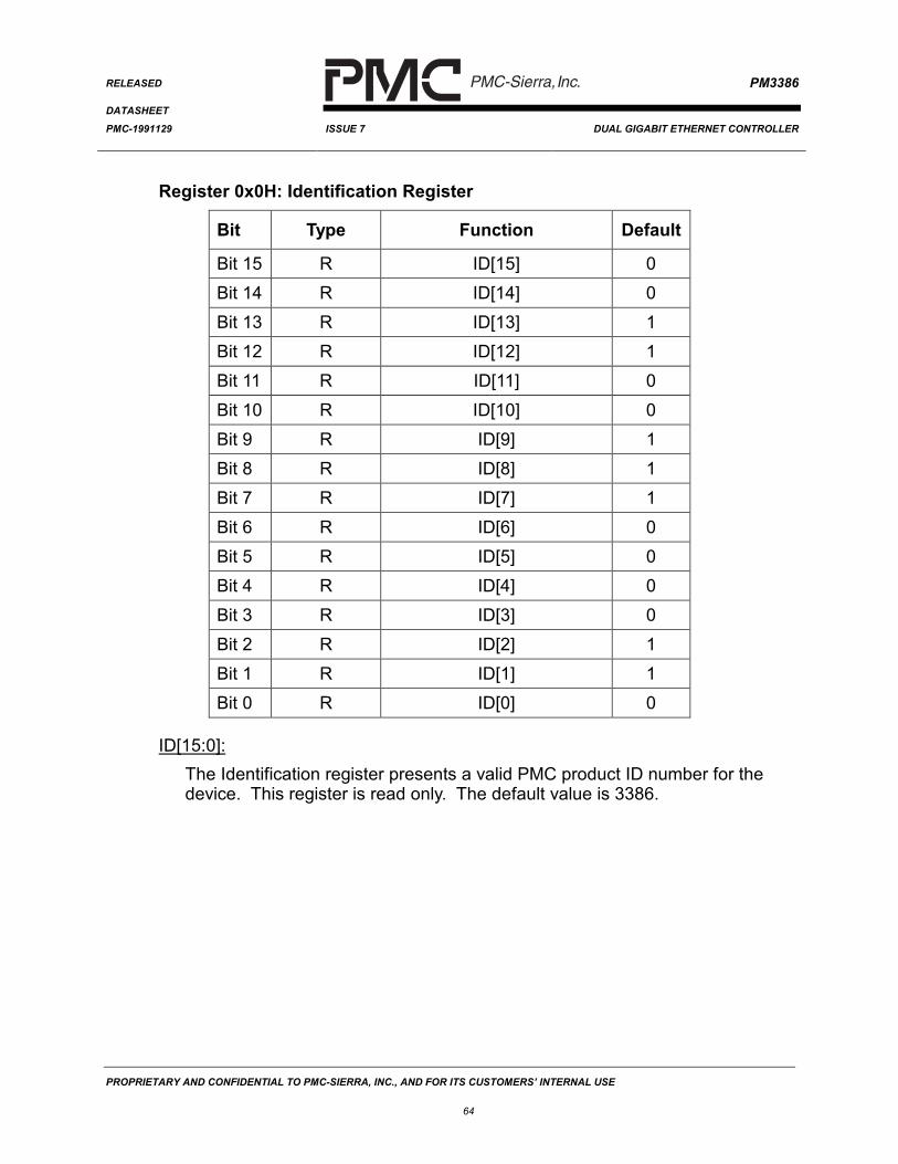
Register 0x0H: Identification Register
Bit Type Function Default
Bit 15 R ID[15] 0Bit 14 R ID[14] 0Bit 13 R ID[13] 1Bit 12 R ID[12] 1Bit 11 R ID[11] 0Bit 10 R ID[10] 0Bit 9 R ID[9] 1Bit 8 R ID[8] 1Bit 7 R ID[7] 1Bit 6 R ID[6] 0Bit 5 R ID[5] 0Bit 4 R ID[4] 0Bit 3 R ID[3] 0Bit 2 R ID[2] 1Bit 1 R ID[1] 1Bit 0 R ID[0] 0
ID[15:0]:The Identification register presents a valid PMC product ID number for thedevice. This register is read only. The default value is 3386.
PROPRIETARY AND CONFIDENTIAL TO PMC-SIERRA, INC., AND FOR ITS CUSTOMERS’ INTERNAL USE
69
Register 0x2H: Reset Control Register
Bit Type Function Default
Bit 15:7 R Reserved 0Bit 6 R/W RESET_PL3EPB 1Bit 5 R/W RESET_PL3IPB 1Bit 4 R/W DIS_STRETCH 0Bit 3:2 R Reserved 0Bit 1 R/W ARESETB 1Bit 0 R/W DRESETB 1
The Reset Control Register generates the reset source output used by blocks inthe PM3386.
DRESETB:Master digital device reset. Performing a hardware reset will clear this bit to a1. Setting this bit to a 0 will cause the digital portion of the device to reset. Itis the responsibility of the programmer to de-assert or set this bit to a one inorder to perform a proper software reset sequence. Please refer to theoperations section of this document for instructions concerning resetting thisdevice using software.
ARESETB:Master analog device reset. Performing a hardware reset will clear this bit toa 1. Setting this bit to a 0 will cause the analog portion of the device to reset.It is the responsibility of the programmer to de-assert or set this bit to a one inorder to perform a proper software reset sequence. Please refer to theoperations section of this document for instructions concerning resetting thisdevice using software.
DIS_STRETCH:By default the internal digital reset is held asserted approximately 10ms afterthe de-assertion of the RSTB pin. To disable this delay the DIS_STRETCHbit can be set to logic 1. This will terminate the internal digital reset delay. Bydefault this bit is disabled. Please refer to the operations section for furtherinformation.
PROPRIETARY AND CONFIDENTIAL TO PMC-SIERRA, INC., AND FOR ITS CUSTOMERS’ INTERNAL USE
70
RESET_PL3IPB:This bit allows for software reset of the PL3IP logic. By default this pin is notasserted or logic 1. To reset the PL3IP the programmer must set this bit tologic 0, wait for a minimum of 100 ns (there is no maximum), and then setthis bit back to logic 1.
RESET_PL3EP:This bit allows for software reset of the PL3EP logic. By default this pin is notasserted or logic 1. To reset the PL3EP the programmer must set this bit tologic 0, wait for a minimum of 100 ns (there is no maximum), and then setthis bit back to logic 1.
PROPRIETARY AND CONFIDENTIAL TO PMC-SIERRA, INC., AND FOR ITS CUSTOMERS’ INTERNAL USE
71
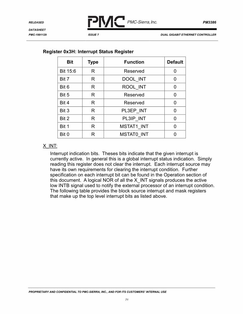
Register 0x3H: Interrupt Status Register
Bit Type Function Default
Bit 15:6 R Reserved 0Bit 7 R DOOL_INT 0Bit 6 R ROOL_INT 0Bit 5 R Reserved 0Bit 4 R Reserved 0Bit 3 R PL3EP_INT 0Bit 2 R PL3IP_INT 0Bit 1 R MSTAT1_INT 0Bit 0 R MSTAT0_INT 0
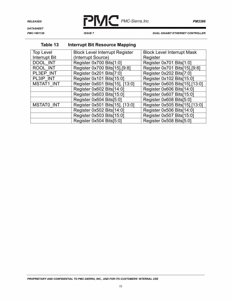
X_INT:Interrupt indication bits. Theses bits indicate that the given interrupt iscurrently active. In general this is a global interrupt status indication. Simplyreading this register does not clear the interrupt. Each interrupt source mayhave its own requirements for clearing the interrupt condition. Furtherspecification on each interrupt bit can be found in the Operation section ofthis document. A logical NOR of all the X_INT signals produces the activelow INTB signal used to notify the external processor of an interrupt condition.The following table provides the block source interrupt and mask registersthat make up the top level interrupt bits as listed above.
PROPRIETARY AND CONFIDENTIAL TO PMC-SIERRA, INC., AND FOR ITS CUSTOMERS’ INTERNAL USE
73
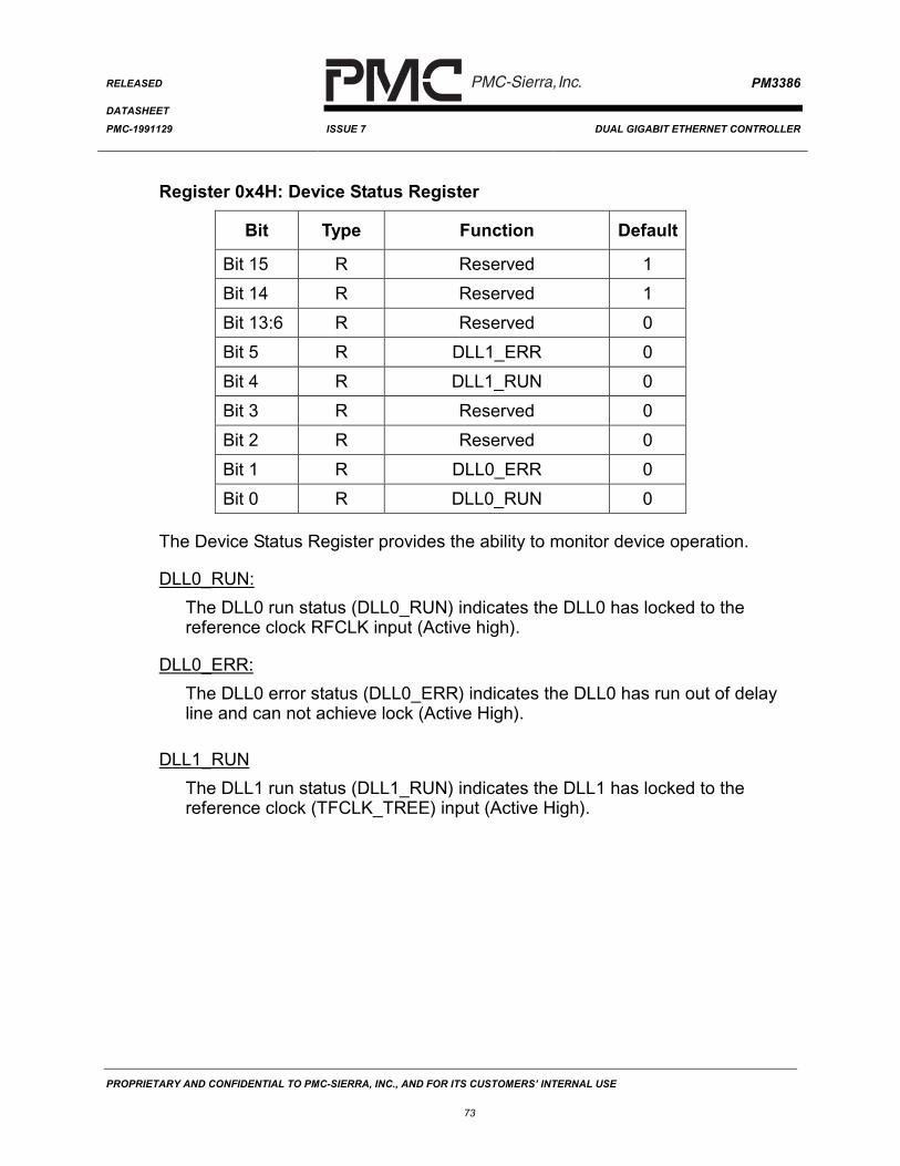
Register 0x4H: Device Status Register
Bit Type Function Default
Bit 15 R Reserved 1Bit 14 R Reserved 1Bit 13:6 R Reserved 0Bit 5 R DLL1_ERR 0Bit 4 R DLL1_RUN 0Bit 3 R Reserved 0Bit 2 R Reserved 0Bit 1 R DLL0_ERR 0Bit 0 R DLL0_RUN 0
The Device Status Register provides the ability to monitor device operation.
DLL0_RUN:The DLL0 run status (DLL0_RUN) indicates the DLL0 has locked to thereference clock RFCLK input (Active high).
DLL0_ERR:The DLL0 error status (DLL0_ERR) indicates the DLL0 has run out of delayline and can not achieve lock (Active High).
DLL1_RUNThe DLL1 run status (DLL1_RUN) indicates the DLL1 has locked to thereference clock (TFCLK_TREE) input (Active High).
PROPRIETARY AND CONFIDENTIAL TO PMC-SIERRA, INC., AND FOR ITS CUSTOMERS’ INTERNAL USE
85
Register 0x7H: Software Resource Register
Bit Type Function Default
Bit 15:0 R/W User_Defined X
User_Defined:The Software Resource register does not control any internal function withinthe PM3386. This register is not reset. This register is read/writeable for useby software.
PROPRIETARY AND CONFIDENTIAL TO PMC-SIERRA, INC., AND FOR ITS CUSTOMERS’ INTERNAL USE
86
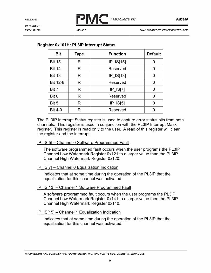
Register 0x101H: PL3IP Interrupt Status
Bit Type Function Default
Bit 15 R IP_IS[15] 0Bit 14 R Reserved 0Bit 13 R IP_IS[13] 0Bit 12-8 R Reserved 0Bit 7 R IP_IS[7] 0Bit 6 R Reserved 0Bit 5 R IP_IS[5] 0Bit 4-0 R Reserved 0
The PL3IP Interrupt Status register is used to capture error status bits from bothchannels. This register is used in conjunction with the PL3IP Interrupt Maskregister. This register is read only to the user. A read of this register will clearthe register and the interrupt.
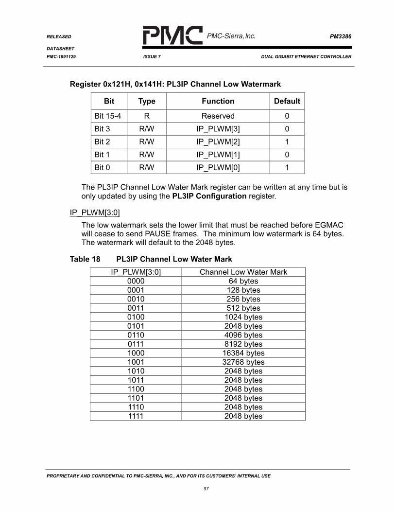
IP_IS[5] – Channel 0 Software Programmed FaultThe software programmed fault occurs when the user programs the PL3IPChannel Low Watermark Register 0x121 to a larger value than the PL3IPChannel High Watermark Register 0x120.
IP_IS[7] – Channel 0 Equalization IndicationIndicates that at some time during the operation of the PL3IP that theequalization for this channel was activated.
IP_IS[13] – Channel 1 Software Programmed FaultA software programmed fault occurs when the user programs the PL3IPChannel Low Watermark Register 0x141 to a larger value then the PL3IPChannel High Watermark Register 0x140.
IP_IS[15] – Channel 1 Equalization IndicationIndicates that at some time during the operation of the PL3IP that theequalization for this channel was activated.
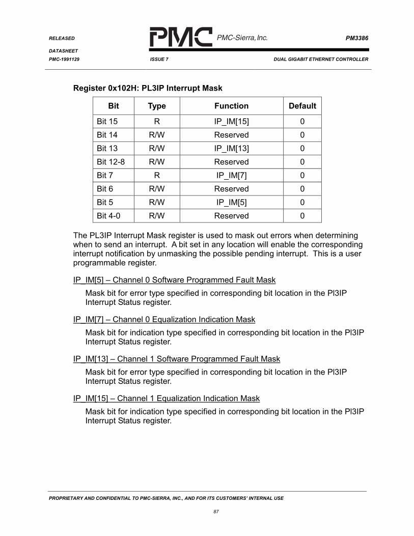
The PL3IP Interrupt Mask register is used to mask out errors when determiningwhen to send an interrupt. A bit set in any location will enable the correspondinginterrupt notification by unmasking the possible pending interrupt. This is a userprogrammable register.
IP_IM[5] – Channel 0 Software Programmed Fault MaskMask bit for error type specified in corresponding bit location in the Pl3IPInterrupt Status register.
IP_IM[7] – Channel 0 Equalization Indication MaskMask bit for indication type specified in corresponding bit location in the Pl3IPInterrupt Status register.
IP_IM[13] – Channel 1 Software Programmed Fault MaskMask bit for error type specified in corresponding bit location in the Pl3IPInterrupt Status register.
IP_IM[15] – Channel 1 Equalization Indication MaskMask bit for indication type specified in corresponding bit location in the Pl3IPInterrupt Status register.
PROPRIETARY AND CONFIDENTIAL TO PMC-SIERRA, INC., AND FOR ITS CUSTOMERS’ INTERNAL USE
88
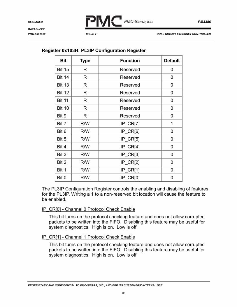
Register 0x103H: PL3IP Configuration Register
Bit Type Function Default
Bit 15 R Reserved 0Bit 14 R Reserved 0Bit 13 R Reserved 0Bit 12 R Reserved 0Bit 11 R Reserved 0Bit 10 R Reserved 0Bit 9 R Reserved 0Bit 7 R/W IP_CR[7] 1Bit 6 R/W IP_CR[6] 0Bit 5 R/W IP_CR[5] 0Bit 4 R/W IP_CR[4] 0Bit 3 R/W IP_CR[3] 0Bit 2 R/W IP_CR[2] 0Bit 1 R/W IP_CR[1] 0Bit 0 R/W IP_CR[0] 0
The PL3IP Configuration Register controls the enabling and disabling of featuresfor the PL3IP. Writing a 1 to a non-reserved bit location will cause the feature tobe enabled.
IP_CR[0] - Channel 0 Protocol Check EnableThis bit turns on the protocol checking feature and does not allow corruptedpackets to be written into the FIFO. Disabling this feature may be useful forsystem diagnostics. High is on. Low is off.
IP_CR[1] - Channel 1 Protocol Check EnableThis bit turns on the protocol checking feature and does not allow corruptedpackets to be written into the FIFO. Disabling this feature may be useful forsystem diagnostics. High is on. Low is off.
PROPRIETARY AND CONFIDENTIAL TO PMC-SIERRA, INC., AND FOR ITS CUSTOMERS’ INTERNAL USE
89
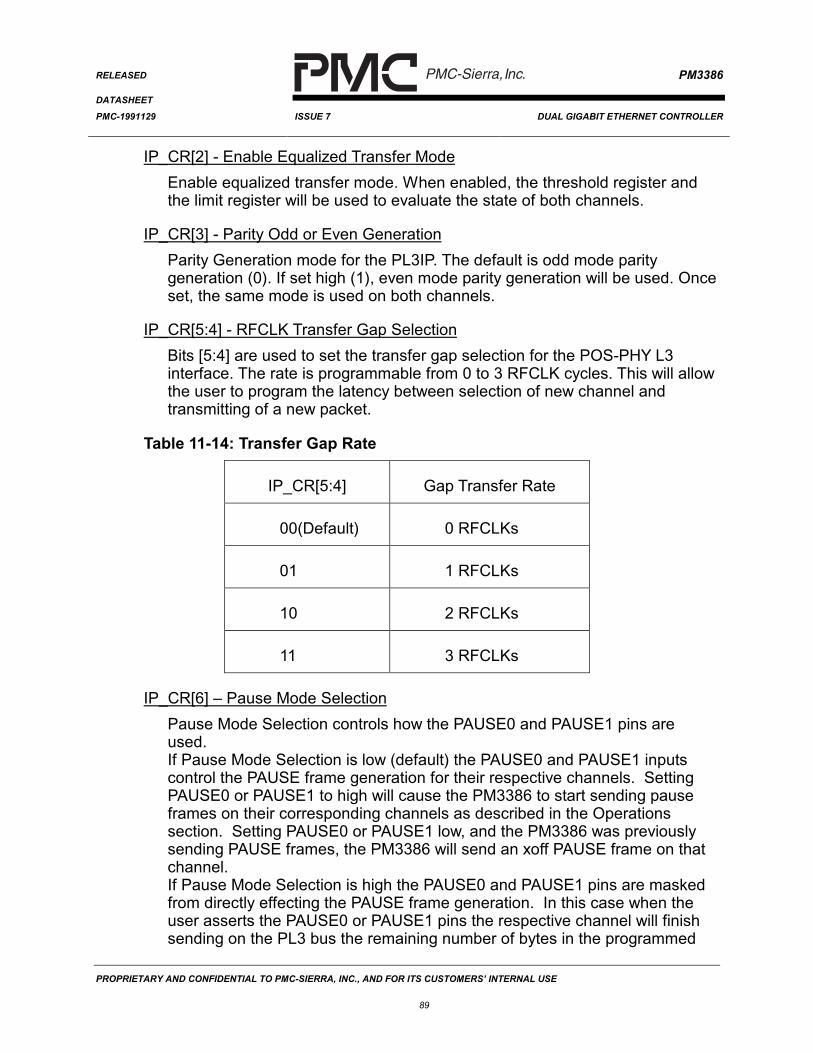
IP_CR[2] - Enable Equalized Transfer ModeEnable equalized transfer mode. When enabled, the threshold register andthe limit register will be used to evaluate the state of both channels.
IP_CR[3] - Parity Odd or Even GenerationParity Generation mode for the PL3IP. The default is odd mode paritygeneration (0). If set high (1), even mode parity generation will be used. Onceset, the same mode is used on both channels.
IP_CR[5:4] - RFCLK Transfer Gap SelectionBits [5:4] are used to set the transfer gap selection for the POS-PHY L3interface. The rate is programmable from 0 to 3 RFCLK cycles. This will allowthe user to program the latency between selection of new channel andtransmitting of a new packet.
Table 11-14: Transfer Gap Rate
IP_CR[5:4] Gap Transfer Rate
00(Default) 0 RFCLKs
01 1 RFCLKs
10 2 RFCLKs
11 3 RFCLKs
IP_CR[6] – Pause Mode SelectionPause Mode Selection controls how the PAUSE0 and PAUSE1 pins areused.If Pause Mode Selection is low (default) the PAUSE0 and PAUSE1 inputscontrol the PAUSE frame generation for their respective channels. SettingPAUSE0 or PAUSE1 to high will cause the PM3386 to start sending pauseframes on their corresponding channels as described in the Operationssection. Setting PAUSE0 or PAUSE1 low, and the PM3386 was previouslysending PAUSE frames, the PM3386 will send an xoff PAUSE frame on thatchannel.If Pause Mode Selection is high the PAUSE0 and PAUSE1 pins are maskedfrom directly effecting the PAUSE frame generation. In this case when theuser asserts the PAUSE0 or PAUSE1 pins the respective channel will finishsending on the PL3 bus the remaining number of bytes in the programmed
PROPRIETARY AND CONFIDENTIAL TO PMC-SIERRA, INC., AND FOR ITS CUSTOMERS’ INTERNAL USE
90
minimum burst size or until EOP is detected and then hold off sending dataon the channel until the PAUSE0 or PAUSE1 pins are de-asserted. Upon de-assertion, if available, data will continue to be transferred across the PL3interface for that channel. Please refer to the Operation section for moredetail on this feature.
IP_CR[7] – Channel EnableChannel Enable is used to update configuration values into the PL3IP whenrequired due to configuration change. The differing PL3IP configurationregisters (0x104, 0x105, 0x120, 0x121, 0x122, 0x140, 0x141, 0x142) may bewritten to at any time but will only update when this bit is cleared. The userprograms the PL3IP configuration registers and then writes a zero to this bitto update the registers within the PL3IP. This bit will automatically return toone when the update is complete..
Bit 15 R Reserved 0Bit 14 R Reserved 0Bit 13 R Reserved 0Bit 12 R Reserved 0Bit 11 R Reserved 0Bit 10 R Reserved 0Bit 9 R Reserved 0Bit 8 R Reserved 0Bit 7 R Reserved 0Bit 6 R Reserved 0Bit 5 R Reserved 0Bit 4 R Reserved 0Bit 3 R Reserved 0Bit 2 R/W IP_ETL[2] 1Bit 1 R/W IP_ETL[1] 1Bit 0 R/W IP_ETL[0] 0
The PL3IP Equalization Threshold Limit is used when the equalized transfermode is enabled. This register can be written at any time but is only updatedinternally by using the PL3IP Configuration register.
IP_ETL[2:0]PL3IP Threshold Limit Register is used to set the upper limit in bytes forequalization support. Please refer to the Operations section for moreinformation on equalization. Table 15 provides the programmable options.
Bit 15 R Reserved 0Bit 14 R Reserved 0Bit 13 R Reserved 0Bit 12 R Reserved 0Bit 11 R Reserved 0Bit 10 R Reserved 0Bit 9 R Reserved 0Bit 8 R Reserved 0Bit 7 R Reserved 0Bit 6 R Reserved 0Bit 5 R Reserved 0Bit 4 R Reserved 0Bit 3 R Reserved 0Bit 2 R/W IP_EDL[2] 1Bit 1 R/W IP_EDL[1] 1Bit 0 R/W IP_EDL[0] 0
The PL3IP Equalization Difference Limit Register is used when the equalizedtransfer mode is enabled. This register can be written at any time but is onlyupdated by using the PL3IP Configuration register.
IP_EDL[2:0]PL3IP Equalization Difference Limit is used to set the maximum difference inbytes between the two channels FIFOs. Default is 32768 bytes, or the 1/2FIFO storage space. The lower limit supported by the hardware is 512 bytes.Please refer to the Operations section for more information on equalization.Table 16 provides the accepted programmable options.
PROPRIETARY AND CONFIDENTIAL TO PMC-SIERRA, INC., AND FOR ITS CUSTOMERS’ INTERNAL USE
95
Register 0x120H, 0x140H: PL3IP Channel High Watermark
Bit Type Function Default
Bit 15 R Reserved 0Bit 14 R Reserved 0Bit 13 R Reserved 0Bit 12 R Reserved 0Bit 11 R Reserved 0Bit 10 R Reserved 0Bit 9 R Reserved 0Bit 8 R Reserved 0Bit 7 R Reserved 0Bit 6 R Reserved 0Bit 5 R Reserved 0Bit 4 R Reserved 0Bit 3 R/W IP_PHWM[3] 0Bit 2 R/W IP_PHWM[2] 1Bit 1 R/W IP_PHWM[1] 1Bit 0 R/W IP_PHWM[0] 0
The PL3IP High Watermark register can be written at any time but is onlyupdated by using the PL3IP Configuration register.
IP_PHWM[3:0]The high water mark sets point at which the EGMAC begins to transmit aPAUSE frame (if enabled). The minimum high watermark is 128 bytes. Thewatermark will default to the 8192 bytes.
The PL3IP Channel Low Water Mark register can be written at any time but isonly updated by using the PL3IP Configuration register.
IP_PLWM[3:0]The low watermark sets the lower limit that must be reached before EGMACwill cease to send PAUSE frames. The minimum low watermark is 64 bytes.The watermark will default to the 2048 bytes.
Table 18 PL3IP Channel Low Water MarkIP_PLWM[3:0] Channel Low Water Mark
The PL3IP Channel Packet Burst Mask register can be written at any time but isonly updated upon channel update using the PL3IP Configuration register.
IP_CFBM[3:0]The packet burst mask determines the amount of data transmitted for onechannel on the PL3 bus before switching to the other channel. If an end ofpacket is detected before the burst limit is reached, the burst will terminateasserting REOP on the PL3 bus. Setting IP_CFBM = 08H enables store-and-forward mode. The PM3386 will store the entire packet into the ingress FIFObefore transmission. The entire packet will be sent on the PL3 bus prior tore-arbitration between the two channels.
0000 16 bytes or EOP0001 32 bytes or EOP0010 64 bytes or EOP0011 128 bytes or EOP0100 256 bytes or EOP0101 512 bytes or EOP0110 1024 bytes or EOP0111 2048 bytes or EOP1XXX Burst till EOP
PROPRIETARY AND CONFIDENTIAL TO PMC-SIERRA, INC., AND FOR ITS CUSTOMERS’ INTERNAL USE
99
Register 0x201H: PL3EP Interrupt Status
Bit Type Function Default
Bit 15 R Reserved 0Bit 14 R Reserved 0Bit 13 R Reserved 0Bit 12 R Reserved 0Bit 11 R Reserved 0Bit 10 R Reserved 0Bit 9 R Reserved 0Bit 8 R Reserved 0Bit 7 R EP_IS[7] 0Bit 6 R Reserved 0Bit 5 R EP_IS[5] 0Bit 4 R Reserved 0Bit 3 R EP_IS[3] 0Bit 2 R Reserved 0Bit 1 R EP_IS[1] 0Bit 0 R Reserved 0
The PL3EP Interrupt Status register is used to capture error status bits from bothPL3EP channels. This register is used in conjunction with the PL3EP InterruptMask register. The register is read only. A read of this register will clear theregister. The status register is written in the same clock domain as the TSB andcan only be written by the TSB. Reads to this register are asynchronous.
EP_IS[1] – Channel 0 FIFO TruncateTruncation occurs when the PL3EP de-asserts DPTA, STPA, or PTPA to theLink Layer and data continues to be sent beyond the programmed limitation,filling all locations in the PL3EP FIFO. The PL3EP will truncate the packet byadding an EOP to the packet internally, assert and internal TERR indication,and ignore all data presented externally until the PL3EP FIFO is capable ofaccepting data.
PROPRIETARY AND CONFIDENTIAL TO PMC-SIERRA, INC., AND FOR ITS CUSTOMERS’ INTERNAL USE
100
EP_IS[3] – Channel 0 PL3 TDAT Parity ErrorTPRTY reported from the PL3 bus interface is different than the internallygenerated parity check for this channel.
EP_IS[5] – Channel 1 FIFO TruncateTruncation occurs when the PL3EP de-asserts DPTA, STPA, or PTPA to theLink Layer and data continues to be sent beyond the programmed limitation,filling all locations in the PL3EP FIFO. The PL3EP will truncate the packet byadding an EOP to the packet internally, assert and internal TERR indication,and ignore all data presented externally until the PL3EP FIFO is capable ofaccepting data.
EP_IS[7] – Channel 1 PL3 TDAT Parity ErrorTPRTY reported from the PL3 bus interface is different than the internallygenerated parity check for this channel.
PROPRIETARY AND CONFIDENTIAL TO PMC-SIERRA, INC., AND FOR ITS CUSTOMERS’ INTERNAL USE
101
Register 0x202H: PL3EP Interrupt Mask
Bit Type Function Default
Bit 15 R Reserved 0Bit 14 R Reserved 0Bit 13 R Reserved 0Bit 12 R Reserved 0Bit 11 R Reserved 0Bit 10 R Reserved 0Bit 9 R Reserved 0Bit 8 R Reserved 0Bit 7 R/W EP_IM[7] 0Bit 6 R/W Reserved 0Bit 5 R/W EP_IM[5] 0Bit 4 R/W Reserved 0Bit 3 R/W EP_IM[3] 0Bit 2 R/W Reserved 0Bit 1 R/W EP_IM[1] 0Bit 0 R/W Reserved 0
The PL3EP Interrupt Mask register is used to mask out errors when determiningwhen to send an interrupt. A bit set in any location other than the reservedlocations, will enable that type of error to cause an interrupt. This is aprogrammable register.
EP_IM[1] – Channel 0 FIFO Truncate MaskMask bit for error type specified in corresponding bit location in the PL3EPInterrupt Status register.
EP_IM[3] – Channel 0 PL3 TDAT Parity Error MaskMask bit for error type specified in corresponding bit location in the PL3EPInterrupt Status register.
PROPRIETARY AND CONFIDENTIAL TO PMC-SIERRA, INC., AND FOR ITS CUSTOMERS’ INTERNAL USE
103
Register 0x203H: PL3EP Configuration Register
Bit Type Function Default
Bit 15 R Reserved 0Bit 14 R Reserved 0Bit 13 R Reserved 0Bit 12 R Reserved 0Bit 11 R Reserved 0Bit 10 R Reserved 0Bit 9 R Reserved 0Bit 8 R Reserved 0Bit 7 R Reserved 0Bit 6 R Reserved 0Bit 5 R Reserved 0Bit 4 R Reserved 0Bit 3 R/W EP_CR[3] 1Bit 2 R/W EP_CR[2] 1Bit 1 R/W EP_CR[1] 0Bit 0 R/W EP_CR[0] 0
The PL3EP Configuration Register controls the enabling and disabling offeatures for the TSB. Writing a 1 to a non-reserved bit location will cause thefeature to be enabled.
EP_CR[0] Parity Checking Enable on TDAT[31:0]This feature will enable the checking of parity on the data from the PL3TDAT[31:0] bus. High is on. Low is off.
EP_CR[1] – Odd or even parity generation and check modeParity Check mode is use to determine whether odd or even mode paritycheck is used across the egress PL3 bus. The default mode is 0 for oddparity. Parity mode applies to both channels.
PROPRIETARY AND CONFIDENTIAL TO PMC-SIERRA, INC., AND FOR ITS CUSTOMERS’ INTERNAL USE
104
EP_CR[2] – Channel 0 UpdateChannel 0 Update is used to update configuration values into the PL3EPwhen required due to configuration change. The differing PL3EPconfiguration registers (0x220, 0x221) may be written to at any time but willonly update when this bit is cleared. The user programs the PL3EPconfiguration registers and then writes a zero to this bit to update theregisters within the channel. This bit will automatically return to one when theupdate is complete.
EP_CR[3] – Channel 1 UpdateChannel 1 Update is used to update configuration values into the PL3EPwhen required due to configuration change. The differing PL3EPconfiguration registers (0x240, 0x241) may be written to at any time but willonly update when this bit is cleared. The user programs the PL3EPconfiguration registers and then writes a zero to this bit to update theregisters within the channel. This bit will automatically return to one when theupdate is complete.
Bit 15-3 R Reserved 0Bit 2 R/W EP_CTR[2] 1Bit 1 R/W EP_CTR[1] 0Bit 0 R/W EP_CTR[0] 1
The PL3EP Channel FIFO Reserve register is user programmable to establishthe amount of reserved FIFO space left once DPTA, STPA, or PTPA have beende-asserted. The default is 2k bytes. This register can be written to at any timebut the internal logic will only be updated by a write to the update bits within thePL3EP configuration register.
EP_CTR[2:0]
Table 20 PM3386 FIFO Reserve Programming OptionsEP_CTR[2:0] Reserve Space in bytes
Bit 15-3 R Reserved 0Bit 2 R/W EP_CMF[2] 0Bit 1 R/W EP_CMF[1] 0Bit 0 R/W EP_CMF[0] 0
The Channel Minimum Frame Size register determines the amount of data togather prior to transmitting the data on the line side via the EGMAC. The logicwill compare the frame size to the frame counter and look at the EOP countbefore pushing data out of the FIFO. If EOP is hit before the minimum framesize is met, the PL3EP will send the completed frame. The default setting is 64bytes of data. This register can be written to at any time but the internal logic willonly be updated by a write to the update bits within the PL3EP Configurationregister.
PROPRIETARY AND CONFIDENTIAL TO PMC-SIERRA, INC., AND FOR ITS CUSTOMERS’ INTERNAL USE
107
Register 0x300H,0x400H: EGMAC - GMACC0 – Config Register Low Word
Bit Type Function DefaultBit 15 R Reserved 0Bit 14 R Reserved 0Bit 13 R Reserved 0Bit 12 R Reserved 0Bit 11 R Reserved 0Bit 10 R Reserved 0Bit 9 R/W L10B 0Bit 8 R/W L32B 0Bit 7 R Reserved 0Bit 6 R Reserved 0Bit 5 R Reserved 0Bit 4 R Reserved 0Bit 3 R Reserved 0Bit 2 R Reserved 0Bit 1 R Reserved 0Bit 0 R/W MIIM PMD_SEL
MIIM:MII Mode select. On reset MIIM takes the value of the PMD_SELx pin. Avalue of logic 1 selects the GMII interface for this channel. A logic value of 0selects the SERDES/TBI interface for this channel.
L32B:Setting this bit will cause the 32-bit transmit packet data to be looped back tothe receive logic in the EGMAC. Clearing this bit results in normal operation,both transmit and receive.
L10B:Setting this bit will cause the 10-bit encoded transmit data to be looped backto the receive logic in the EGMAC. Clearing this bit results in normaloperation, both transmit and receive.
Please note that after updating this register a software reset of the state logic isrequired using the SRST bit in EGMAC GMACC0 – Config Register High WordRegister
PROPRIETARY AND CONFIDENTIAL TO PMC-SIERRA, INC., AND FOR ITS CUSTOMERS’ INTERNAL USE
108
Register 0x301H,0x401H: EGMAC - GMACC0 – Config Register High Word
Bit Type Function DefaultBit 15 R/W SRST 0Bit 14 R Reserved 0Bit 13 R Reserved 0Bit 12 R Reserved 0Bit 11 R Reserved 0Bit 10 R Reserved 0Bit 9 R Reserved 0Bit 8 R Reserved 0Bit 7 R Reserved 0Bit 6 R Reserved 0Bit 5 R Reserved 0Bit 4 R Reserved 0Bit 3 R Reserved 0Bit 2 R Reserved 0Bit 1 R Reserved 0Bit 0 R Reserved 0
SRST:Soft Reset. Setting this bit will reset the internal state of the EGMAC blockand load register settings from registers 0x300-0x305 or 0x400-0x405. Note:Registers 0x300-0x305 or 0x400-0x405 will retain their written value. This bitshould be set whenever changes are made to the register bits found inregister 0x300-0x305 or 0x400-0x405 except for the TXEN0 and RXEN0 bits.To reset / update state first write a 1 to SRST and then write a 0.Note that the address filter registers 0x339-0x35F or 0x439-0x45F are resetby the use of the SRST bit. The pre-update registers within the PM3386 willalways contain the last loaded address filter information so it is possible towrite to register 0x360 or 0x460 Update bit to restore the PM3386 addressfiltering registers to pre-software reset condition.
PROPRIETARY AND CONFIDENTIAL TO PMC-SIERRA, INC., AND FOR ITS CUSTOMERS’ INTERNAL USE
109
Register 0x302H,0x402H: EGMAC - GMACC1 – Config Register Low Word
Bit Type Function DefaultBit 15 R Reserved 0Bit 14 R Reserved 0Bit 13 R Reserved 0Bit 12 R/W LONGP 0Bit 11 R Reserved 0Bit 10 R/W FCRX 0Bit 9 R/W FCTX 0Bit 8 R/W PUREP 1Bit 7 R Reserved 0Bit 6 R Reserved 0Bit 5 R/W FLCHK 0Bit 4 R/W CRCEN 0Bit 3 R Reserved 0Bit 2 R Reserved 0Bit 1 R/W PADEN 1Bit 0 R FULLD 1
FULLD:Full-Duplex. This bit is always set to 1 to indicate that the MAC is always inFull-Duplex mode.
PADEN:Pad Enable. Pad frames including VID field with 0’s to 60 bytes (if necessary)and append CRC thereby ensuring minimum frame size of 64 bytes.
CRCEN:CRC Enable. Set this bit to have the MAC append a CRC on each and everyframe it transmits. Clear this bit when frames from the system already have avalid CRC. Note: Frames are always checked for a valid CRC.
FLCHK:Frame Length Check. Set this bit to allow the MAC to check the length ofreceived frames. The MAC will then check all frames whose length/type fieldrepresents a valid length (46-1500 octets) comparing the value in thelength/type field to the actual LLC data field length.
PROPRIETARY AND CONFIDENTIAL TO PMC-SIERRA, INC., AND FOR ITS CUSTOMERS’ INTERNAL USE
110
PUREP:Pure Preamble. Set this bit to cause the EGMAC to check the content of thepreamble field of the packet, ensuring a data pattern of 0x55. Clear this bit ifno preamble checking is desired. The length of the preamble is not checkedin either case.
FCTX:Flow Control: Transmit Capable. Setting this bit allows the MAC Control sub-layer to transmit PAUSE Control frames. Clearing this bit prevents thetransmission of internally generated PAUSE frames. Please note that it isillegal to enable the FCTX bit without enabling the PADEN bit. However it islegal to enable the PADEN bit without enabling the FCTX bit.
FCRX:Flow Control: Receive Capable. Setting this bit allows the MAC Control sub-layer to respond to PAUSE Control frames by pausing the transmitter fromtransmitting data frames. Transmit pause control frames are still allowed to betransmitted if they are triggered by internal FIFO fill levels or via the PAUSEpin. Clearing this bit prevents any action based on the reception of PAUSEframes. Note that the PM3386 PAUSE counter will always reflect the PAUSEquanta as updated by incoming PAUSE frames. The PM3386 will only actupon (by ceasing transmit traffic) the non zero PAUSE counter if FCRX ishigh. The PAUSED0 or PAUSED1 will always reflect the status of thecorresponding channels PAUSE counter.
LONGP:Accept Preambles Over 12 Bytes. If LONGP is disabled, packets withpreambles > 12 bytes will be dropped.
Please note that after updating this register a software reset of the state logic isrequired using the SRST bit in EGMAC GMACC0 – Config Register High WordRegister
PROPRIETARY AND CONFIDENTIAL TO PMC-SIERRA, INC., AND FOR ITS CUSTOMERS’ INTERNAL USE
111
Register 0x303H,0x403H: EGMAC - GMACC1 – Config Register High Word
Bit Type Function DefaultBit 15 R Reserved 0Bit 14 R/W TXEN0 0Bit 13 R Reserved 0Bit 12 R/W RXEN0 0Bit 11 R Reserved 0Bit 10 R Reserved 0Bit 9 R Reserved 0Bit 8 R Reserved 0Bit 7 R Reserved 0Bit 6 R Reserved 0Bit 5 R Reserved 0Bit 4 R Reserved 0Bit 3 R Reserved 0Bit 2 R Reserved 0Bit 1 R/W Reserved 0Bit 0 R/W Reserved 0
RXEN0:Receive Enable. Enables device receive operations. When set low (resetdefault) the receive or ingress direction of the device will cease to transferdata. Traffic will be dropped at the EGMAC interface until the assertion ofRXEN0. When set high the PM3386 will allow frame data to be transferred.
TXEN0:Transmit Enable. Enables possible transmit operations. Upon device resetthis bit will be set low. This will disable all transmit or egress traffic flow forthis port. To enable possible egress traffic flow this bit must be set to one.This bit should not be used by the programmer to halt transmit data flow asthe TPAUSE bit within the EGMAC Transmit Control register is responsiblefor this function. Please see enabling and disabling data flows in theOperation section for more in formation.
PROPRIETARY AND CONFIDENTIAL TO PMC-SIERRA, INC., AND FOR ITS CUSTOMERS’ INTERNAL USE
112
Register 0x304H,0x404H: EGMAC - GMACC2 – Config Register Low Word
Bit Type Function DefaultBit 15 R Reserved 0Bit 14 R Reserved 0Bit 13 R Reserved 0Bit 12 R Reserved 0Bit 11 R Reserved 0Bit 10 R Reserved 0Bit 9 R Reserved 0Bit 8 R Reserved 0Bit 7 R Reserved 0Bit 6 R Reserved 0Bit 5 R/W IPGT[5] 0Bit 4 R/W IPGT[4] 0Bit 3 R/W IPGT[3] 1Bit 2 R/W IPGT[2] 1Bit 1 R/W IPGT[1] 0Bit 0 R/W IPGT[0] 0
IPGT[5:0]:Back-to-Back Transmit IPG. This is a programmable field representing theIPG between back-to-back packets. Set this field to the number of octets ofIPG desired. A setting of 12 decimal represents the minimum IPG of 0.096µs.
Please note that after updating this register a software reset of the state logic isrequired using the SRST bit in EGMAC GMACC0 – Config Register High WordRegister
PROPRIETARY AND CONFIDENTIAL TO PMC-SIERRA, INC., AND FOR ITS CUSTOMERS’ INTERNAL USE
114
Register 0x305H,0x405H: EGMAC - GMACC2 – Config Register High Word
Bit Type Function DefaultBit 15 R Reserved 0Bit 14 R Reserved 0Bit 13 R Reserved 0Bit 12 R Reserved 0Bit 11 R Reserved 0Bit 10 R Reserved 0Bit 9 R Reserved 0Bit 8 R Reserved 0Bit 7 R Reserved 0Bit 6 R Reserved 0Bit 5 R Reserved 0Bit 4 R/W SPRE 0Bit 3 R Reserved 0Bit 2 R Reserved 0Bit 1 R Reserved 0Bit 0 R Reserved 0
SPRESuppress Preamble bit. This bit if set to 1 will suppress the MII Managementpreamble on the MDIO pin.
Please note that after updating this register a software reset of the state logic isrequired using the SRST bit in EGMAC GMACC0 – Config Register High WordRegister
PROPRIETARY AND CONFIDENTIAL TO PMC-SIERRA, INC., AND FOR ITS CUSTOMERS’ INTERNAL USE
115
Register 0x306H,0x406H: EGMAC - GPCSC – PHY Config Low Word
Bit Type Function DefaultBit 15 R Reserved 0Bit 14 R/W Reserved 0Bit 13 R/W Reserved 0Bit 12 R/W Reserved 0Bit 11 R Reserved 0Bit 10 R Reserved 0Bit 9 R Reserved 0Bit 8 R/W AUTOS 0Bit 7 R Reserved 0Bit 6 R Reserved 0Bit 5 R Reserved 0Bit 4 R Reserved 0Bit 3 R Reserved 0Bit 2 R Reserved 0Bit 1 R Reserved 0Bit 0 R Reserved 0
AUTOS:Auto Sense Auto-Neg Status. When asserted this bit will cause the MAC toauto sense if Link Partner is in Link Bypass mode or in Auto-negotiationmode.
JTRPT[9:0]:Custom Jitter Pattern. Used in conjunction with JITTERN PATTERN SELECTand JITTER DIAGNOSTIC ENABLE, set this field to the desired custompattern which will be continuously transmitted.
Table 23 Jitter Pattern TableJTRPS[2:0] 40 bit Data Transmitted to SERDES Comments
000b 1111100000111110000011111000001111100000… Low Freq.001b 1111101011000001010011111010110000010100… Mixed Freq.010b 1010101010101010101010101010101010101010… High Freq.011b See Custom Jitter Pattern, bits [25:16] User Def’d.1XXb Reserved Reserved
JTRPS[2:0]:Jitter Pattern Select. Selects the jitter pattern to be transmitted in diagnosticsmode. See Jitter Table above.
PROPRIETARY AND CONFIDENTIAL TO PMC-SIERRA, INC., AND FOR ITS CUSTOMERS’ INTERNAL USE
117
JTRDE:Jitter Diagnostic Enable. Set this bit to enable the GMAC to transmit the jittertest patterns defined in IEEE 802.3z 36A. Clear this bit to enable normaltransmit operation.
PROPRIETARY AND CONFIDENTIAL TO PMC-SIERRA, INC., AND FOR ITS CUSTOMERS’ INTERNAL USE
118
Register 0x308H,0x408H: EGMAC - SA – Station Address [15:0]
Bit Type Function DefaultBit 15 R/W SA[15] 0Bit 14 R/W SA [14] 0Bit 13 R/W SA [13] 0Bit 12 R/W SA [12] 0Bit 11 R/W SA [11] 0Bit 10 R/W SA [10] 0Bit 9 R/W SA [9] 0Bit 8 R/W SA [8] 0Bit 7 R/W SA [7] 0Bit 6 R/W SA [6] 0Bit 5 R/W SA [5] 0Bit 4 R/W SA [4] 0Bit 3 R/W SA [3] 0Bit 2 R/W SA [2] 0Bit 1 R/W SA [1] 0Bit 0 R/W SA [0] 0
SA[15:0]:Station Address Low word.
Please note that a station address (SA) of SA[47:0] = 0x1234_5678_9ABC would beseen on the wire and by the MAC with the least significant bit of the least significantbyte of SA[7:0] being first. In this case the MAC will receive and transmit data with theabove example SA as BC_9A_78_56_34_12. Please refer to Table 32 and Table 33 inthis document and IEEE 802.3-1998 Section 3.2.3 for reference.
PROPRIETARY AND CONFIDENTIAL TO PMC-SIERRA, INC., AND FOR ITS CUSTOMERS’ INTERNAL USE
119
Register 0x309H,0x409H: EGMAC - SA – Station Address [31:16]
Bit Type Function DefaultBit 15 R/W SA[31] 0Bit 14 R/W SA [30] 0Bit 13 R/W SA [29] 0Bit 12 R/W SA [28] 0Bit 11 R/W SA [27] 0Bit 10 R/W SA [26] 0Bit 9 R/W SA [25] 0Bit 8 R/W SA [24] 0Bit 7 R/W SA [23] 0Bit 6 R/W SA [22] 0Bit 5 R/W SA [21] 0Bit 4 R/W SA [20] 0Bit 3 R/W SA [19] 0Bit 2 R/W SA [18] 0Bit 1 R/W SA [17] 0Bit 0 R/W SA [16] 0
PROPRIETARY AND CONFIDENTIAL TO PMC-SIERRA, INC., AND FOR ITS CUSTOMERS’ INTERNAL USE
120
Register 0x30aH,0x40aH: EGMAC - SA – Station Address [47:32]
Bit Type Function DefaultBit 15 R/W SA[47] 0Bit 14 R/W SA [46] 0Bit 13 R/W SA [45] 0Bit 12 R/W SA [44] 0Bit 11 R/W SA [43] 0Bit 10 R/W SA [42] 0Bit 9 R/W SA [41] 0Bit 8 R/W SA [40] 0Bit 7 R/W SA [39] 0Bit 6 R/W SA [38] 0Bit 5 R/W SA [37] 0Bit 4 R/W SA [36] 0Bit 3 R/W SA [35] 0Bit 2 R/W SA [34] 0Bit 1 R/W SA [33] 0Bit 0 R/W SA [32] 0
TPID[15:0]:Tag Protocol Identifier. Program this field with the 16-bit VLAN TPID. TheMAC will detect VLAN tagged frames by comparing the two bytes followingthe Source Address with this field. The VLAN TPID defined by 802.1Q is0x8100.
RX_MAXFR[15:0]:This field defaults to 0x05EE, which represents a maximum receive frame of1518 octets. An untagged maximum size Ethernet frame is 1518 octets inlength. A tagged frame adds four octets for a total of 1522 octets. The framewill be truncated to match the specified length. Note: This field only affectsthe reception of frames. Also note the addition of 4 bytes for a VLAN taggedframe.
PROPRIETARY AND CONFIDENTIAL TO PMC-SIERRA, INC., AND FOR ITS CUSTOMERS’ INTERNAL USE
123
Table 24 Max frame size conditionsRegisterSetting
ReceivedSize
CRCindication
VLANTagged
Result
1518 1518 Good N/A Good frame1518 1518 Bad N/A CRC erred frame1518 1519 Good No Length erred frame1518 1519 Bad No Jabber erred frame1518 1519 Good Yes Good frame1518 1519 Bad Yes CRC erred frame1518 1522 Good Yes Good frame1518 1522 Bad Yes CRC erred frame1518 1523 Good Yes Length erred frame1518 1523 Bad Yes Jabber erred frame
PROPRIETARY AND CONFIDENTIAL TO PMC-SIERRA, INC., AND FOR ITS CUSTOMERS’ INTERNAL USE
124
Register 0x318H,0x418H: EGMAC - ANCTL – Auto-Negotiation Control
Bit Type Function DefaultBit 15 R Reserved 0Bit 14 R Reserved 0Bit 13 R Reserved 0Bit 12 R Reserved 0Bit 11 R Reserved 0Bit 10 R Reserved 0Bit 9 R Reserved 0Bit 8 R Reserved 0Bit 7 R Reserved 0Bit 6 R Reserved 0Bit 5 R Reserved 0Bit 4 R Reserved 0Bit 3 R Reserved 0Bit 2 R Reserved 0Bit 1 R/W ANEN 0Bit 0 R/W RSTAN 0
RSTAN:Restart Auto-Negotiation. Setting this bit to a 1 then to a 0 will restart theAuto-Negotiation Process..
ANEN:Auto-Negotiation Enable. Setting this bit enables Auto-Negotiation Process.Clearing it will prevent auto negotiation and puts the EGMAC in LINKBYPASS mode.
PROPRIETARY AND CONFIDENTIAL TO PMC-SIERRA, INC., AND FOR ITS CUSTOMERS’ INTERNAL USE
125
Register 0x31AH,0x41AH: EGMAC - ANSTT – Auto-Negotiation Status
Bit Type Function DefaultBit 15 R Reserved 0Bit 14 R Reserved 0Bit 13 R Reserved 0Bit 12 R Reserved 0Bit 11 R Reserved 0Bit 10 R Reserved 0Bit 9 R Reserved 0Bit 8 R Reserved 0Bit 7 R Reserved 0Bit 6 R Reserved 0Bit 5 R Reserved 0Bit 4 R RFIND 0Bit 3 R ANCPLT 0Bit 2 R PGRX 0Bit 1 R LINKOK 0Bit 0 R SYNCOK 0
SYNCOK:Synchronization Status. Asserted after receiving three valid Idle ordered setssignaling comma detect lock achieved.
LINKOK:Link OK. This can be asserted by two different means.1. The SYNCOK bit is asserted (I.E. comma detect achieved) and the ANENbit in the Auto Negotiation Status register is 1 and auto-negotiation iscomplete.2. The SYNCOK bit is asserted (I.E> comma detect achieved) and the ANENbit in the Auto Negotiation Status register is 0. (Auto-negotiation status isignored).Please note that the LINKOK bit is implemented with a latch implementation.To get the current status the LINKOK must be read once for past status andtwice to get current status.
PGRX:Page Received. MII Mgmt register 6 bit [1]. When ‘1’ – a new page has beenreceived. When ‘0’ – a new page has not been received. This bit is clearedupon reading this register.
Bit Type Function DefaultMII Mgmt Register 4: Base Page
Bit 15 R/W NEXTP 0Bit 14 R Reserved 0Bit 13 R/W ANERR[1] 0Bit 12 R/W ANERR[0] 0Bit 11 R Reserved 0Bit 10 R Reserved 0Bit 9 R Reserved 0Bit 8 R/W ASMDR/PAUSE[1] 1Bit 7 R/W ASMDR/PAUSE[0] 1Bit 6 R Reserved 0Bit 5 R/W FD 1Bit 4 R Reserved 0Bit 3 R Reserved 0Bit 2 R Reserved 0Bit 1 R Reserved 0Bit 0 R Reserved 0
FD:Full-Duplex. Setting this bit means local device is capable of full-duplexoperation. This bit should be set to a ‘1’ for normal operation.
ASMDR/PAUSE[1:0]:Local PAUSE Capabilities. The local device’s PAUSE capability is encoded inbits 8:7, and the decodes are shown in Pause Encoding Table below. Forpriority resolution between link partner and local pause capabilities, consultPause Priority Resolution Table.
PROPRIETARY AND CONFIDENTIAL TO PMC-SIERRA, INC., AND FOR ITS CUSTOMERS’ INTERNAL USE
128
ANERR[1:0]:Auto-Neg Error. The local device’s remote fault condition may be encoded inbits 13:12 of the base page. Values are shown in Remote Fault EncodingTable 26 shown below. The default value is 0b00. Local device may indicate afault by setting a non-zero Remote Fault encoding and re-negotiating.
0 0 No error, link OK0 1 Offline1 0 Link_Failure1 1 Auto-Negotiation_Error
NEXTP:Next Page Capable. The local device asserts this bit to request next pagetransmission. Clear this bit when local device has no subsequent next pages.
NPLPCF[10:0]:Next Page Local Code Field. This field contains the data that is sent in thenext page. Message pages are formatted pages that carry a predefinedMessage Code, which is enumerated in IEE 802.3u/Annex 28C. UnformattedCode Fields take on an arbitrary value.
ANTOG:Link Partner Toggle. Used to ensure synchronization with the Link Partnerduring Next Page exchange. This bit always takes opposite value of theToggle bit of the previously exchanged Link Code Word. The initial value inthe first Next Page transmitted is the inverse of bit 11 in the base Link CodeWord.
ANACK2:Auto-Neg Acknowledge 2. Used by next page function to indicate device hasability to comply with the message. Assert bit if local device will comply withmessage. Clear bit if local device cannot comply with message.
PROPRIETARY AND CONFIDENTIAL TO PMC-SIERRA, INC., AND FOR ITS CUSTOMERS’ INTERNAL USE
131
Register 0x31EH,0x41EH: EGMAC - ANLPA – Auto-Negotiation Link PartAble Low Word
Bit Type Function DefaultMII Mgmt Register 5
Bit 15 R LPNEXTP 0Bit 14 R ACKNOWLEDGE 0Bit 13 R LPANERR[1] 0Bit 12 R LPANERR[0] 0Bit 11 R Reserved 0Bit 10 R Reserved 0Bit 9 R Reserved 0Bit 8 R LPASMDR/
LPPAUSE[1]0
Bit 7 R LPASMDR/LPPAUSE[0]
0
Bit 6 R Reserved 0Bit 5 R LPFD 0Bit 4 R Reserved 0Bit 3 R Reserved 0Bit 2 R Reserved 0Bit 1 R Reserved 0Bit 0 R Reserved 0
LPFD:LP Full-Duplex. When ‘1’ – link partner is capable of Full-Duplex operation.When ‘0’ – link partner is incapable of Full-Duplex mode.
LPASMDR/LPPAUSE[1:0]:LP Asymmetric Direction / LP Pause. Encoding of the link partner’s PAUSEcapability is shown in Pause Encoding Table. For priority resolution betweenlink partner and local pause capabilities consult Pause Priority ResolutionTable.
LPANERR[1:0]:LP Remote Fault. The link partner’s remote fault condition is encoded in bits13:12 of the base page. Values are shown in Remote Fault Encoding Table.
ACKNOWLEDGE:The ACKNOWLEDGE bit in the Link Partner’s base page indicates that adevice has successfully received its link partner’s base page.
PROPRIETARY AND CONFIDENTIAL TO PMC-SIERRA, INC., AND FOR ITS CUSTOMERS’ INTERNAL USE
133
Register 0x31FH,0x41FH: EGMAC - ANLPA – Auto-Negotiation Link PartAble High Word
Bit Type Function DefaultMII Mgmt Register 8
Bit 15 R LPNP 0Bit 14 R ACKNOWLEDGE 0Bit 13 R LPMSG 0Bit 12 R LPACK2 0Bit 11 R LPTOG 0Bit 10 R LPCF[10] 0Bit 9 R LPCF[9] 0Bit 8 R LPCF[8] 0Bit 7 R LPCF[7] 0Bit 6 R LPCF[6] 0Bit 5 R LPCF[5] 0Bit 4 R LPCF[4] 0Bit 3 R LPCF[3] 0Bit 2 R LPCF[2] 0Bit 1 R LPCF[1] 0Bit 0 R LPCF[0] 0
LPCF[10:0]:LP Code Field. Message Pages are formatted pages that carry a predefinedMessage Code, which is enumerated in IEEE 802.3u/Annex 28C.
LPTOG:LP Toggle. Used to ensure synchronization with the Link Partner during NextPage exchange. This bit always takes opposite value of the Toggle bit of thepreviously exchanged Link Code Word. The initial value in the first Next Pagetransmitted is the inverse of bit 11 in the base Link Code Word.
LPACK2:LP Acknowledge 2. Indicates link partner’s ability to comply with themessage. When ‘1’ – link partner will comply with message. When ‘0’ – linkpartner cannot comply with message.
LPMSG:LP Message Page. When ‘1’ – indicates Message Page. When ‘0’ – indicatesUnformatted Page.
PROPRIETARY AND CONFIDENTIAL TO PMC-SIERRA, INC., AND FOR ITS CUSTOMERS’ INTERNAL USE
134
ACKNOWLEDGE:The ACKNOWLEDGE bit in the Link Partner’s next page register is used toindicate that the device has successfully received its link partner’s next page.
LPNP:LP Next Page. The link partner asserts this bit to request next pagetransmission. When ‘0’ – link partner has no subsequent next pages.
PROPRIETARY AND CONFIDENTIAL TO PMC-SIERRA, INC., AND FOR ITS CUSTOMERS’ INTERNAL USE
135
Register 0x320H: EGMAC - MCMD – MII Management Command
Bit Type Function DefaultBit 15 R Reserved 0Bit 14 R Reserved 0Bit 13 R Reserved 0Bit 12 R Reserved 0Bit 11 R Reserved 0Bit 10 R Reserved 0Bit 9 R Reserved 0Bit 8 R Reserved 0Bit 7 R Reserved 0Bit 6 R Reserved 0Bit 5 R Reserved 0Bit 4 R Reserved 0Bit 3 R Reserved 0Bit 2 R Reserved 0Bit 1 R Reserved 0Bit 0 R/W RSTAT 0
RSTAT:MII Management Read Status. Writting this bit to a 1 causes a read operationon the register addressed by EGMAC MADR: MII Management PHY Address.Upon completion of the MII read as outlined within the Operations section MIIRead Access instructions the RSTAT bit must be cleared to 0.
PROPRIETARY AND CONFIDENTIAL TO PMC-SIERRA, INC., AND FOR ITS CUSTOMERS’ INTERNAL USE
138
Register 0x326H: EGMAC - MRDD – MII Management Read Data
Bit Type Function DefaultBit 15 R PRSD[15] 0Bit 14 R PRSD [14] 0Bit 13 R PRSD [13] 0Bit 12 R PRSD [12] 0Bit 11 R PRSD [11] 0Bit 10 R PRSD [10] 0Bit 9 R PRSD [9] 0Bit 8 R PRSD [8] 0Bit 7 R PRSD [7] 0Bit 6 R PRSD [6] 0Bit 5 R PRSD [5] 0Bit 4 R PRSD [4] 0Bit 3 R PRSD [3] 0Bit 2 R PRSD [2] 0Bit 1 R PRSD [1] 0Bit 0 R PRSD [0] 0
PRSD[15:0]:Read Status Data. The 16-bit results from the read operation of registeraddressed using the EGMAC – MADR: MII Management PHY register.
PROPRIETARY AND CONFIDENTIAL TO PMC-SIERRA, INC., AND FOR ITS CUSTOMERS’ INTERNAL USE
139
Register 0x328H: EGMAC - MIND – MII Management Indicators
Bit Type Function DefaultBit 15 R Reserved 0Bit 14 R Reserved 0Bit 13 R Reserved 0Bit 12 R Reserved 0Bit 11 R Reserved 0Bit 10 R Reserved 0Bit 9 R Reserved 0Bit 8 R Reserved 0Bit 7 R Reserved 0Bit 6 R Reserved 0Bit 5 R Reserved 0Bit 4 R Reserved 0Bit 3 R Reserved 0Bit 2 R Reserved 0Bit 1 R Reserved 0Bit 0 R MBSY 0
MBSY:MIIM Busy. Management operation in progress. MBSY goes active when aregister is written to, or read from or during a SCAN operation and staysactive until the end of the respective operation. The read status data is onlyvalid when MBSY is inactive.
PROPRIETARY AND CONFIDENTIAL TO PMC-SIERRA, INC., AND FOR ITS CUSTOMERS’ INTERNAL USE
140
Register 0x332H,0x432H: EGMAC – Transmit Control
Bit Type Function DefaultBit 15 R Reserved 0Bit 14 R Reserved 0Bit 13 R Reserved 0Bit 12 R Reserved 0Bit 11 R Reserved 0Bit 10 R Reserved 0Bit 9 R Reserved 0Bit 8 R Reserved 0Bit 7 R Reserved 0Bit 6 R Reserved 0Bit 5 R Reserved 0Bit 4 R Reserved 0Bit 3 R Reserved 0Bit 2 R Reserved 0Bit 1 R/W TPAUSE 0Bit 0 R/W SPQCT 0
SPQCT:Shortcut Pause Quanta Counter. When asserted this bit causes the PauseQuanta time to be changed form 512 byte times to 1 bit time. This bit is fortesting purposes only and should be cleared for normal operation.
TPAUSE:The TPAUSE bit directs the EGMAC to gracefully halt transmit traffic. Whenset the EGMAC will halt transmit traffic. When cleared the EGMAC willresume egress data transfer. When halted the egress traffic will accumulatein the PM3386 egress FIFO and upon de-assertion of the TPAUSE bit thedata will resume transmission.
PROPRIETARY AND CONFIDENTIAL TO PMC-SIERRA, INC., AND FOR ITS CUSTOMERS’ INTERNAL USE
141
Register 0x333H,0x433H: EGMAC - CONTROL – EGMAC Control Register
Bit Type Function DefaultBit 15 R Reserved 0Bit 14 R Reserved 0Bit 13 R Reserved 0Bit 12 R Reserved 0Bit 11 R Reserved 0Bit 10 R Reserved 0Bit 9 R Reserved 0Bit 8 R Reserved 0Bit 7 R Reserved 0Bit 6 R Reserved 0Bit 5 R:W Reserved 0Bit 4 R/W PASS_CTRL 0Bit 3 R/W PASS_ERRORS 0Bit 2 R/W HOSTPAUSE 0Bit 1 R/W Reserved 0Bit 0 R/W Reserved 0
HOSTPAUSE: HOST PAUSE enable bit. When set to a 1 the EGMAC will send PAUSEControl Frames based on the PAUSE timer and PAUSE interval registers.Setting the bit to a 0 will cause the EGMAC to no longer send PAUSE ControlFrames and if currently in a PAUSE state will send a PAUSE control framewith a pause timer value set to zero.
PASS_ERRORS: PASS_ERRORS enable bit. When set to a 1 the EGMAC will forward allerred frames to the system FIFO interface. Setting the bit to a 0 will cause theEGMAC to filter all erred frames.
PASS_CTRL: PASS_CTRL enable bit. When set to a 1 the EGMAC will forward all receivedcontrol frames to the system FIFO interface. Setting the bit to a 0 the EGMACwill filter all control frames.
PAUSE_TIME[15:0]:Pause Timer value that is used on the PAUSE Control Frames that are sentto the downstream PHY. The default is 0xFFFF for a XON/XOFF type ofprotocol.
TX_MAXFR [15:0]:Specifies the maximum number of bytes that are allowed to be transmittedbefore truncation in an outgoing normal Ethernet frame. Default = 1518 bytes> 5EE Hex. Frames that have exceeded the TX_MAXFR setting will betruncated having a 4 byte erred CRC appended to them. Please note thatVLAN tagged frames have a 4 byte offset (i.e. 1522 bytes) before beingconsidered as violating the frame length setting and therefore beingtruncated. The total transmitted frame size for frames violating the maximumtransmit frame size will be TX_MAXFR + 4 for non tagged frames andTX_MAXFR + 8 for tagged frames. Please note that supported values forthis register are from 1518 to 9600 bytes.
Bit Type Function DefaultBit 15 R Reserved 0Bit 14 R Reserved 0Bit 13 R Reserved 0Bit 12 R Reserved 0Bit 11 R/W RXFIFO_FWD[11] 0Bit 10 R/W RXFIFO_FWD[10] 0Bit 9 R/W RXFIFO_FWD[9] 0Bit 8 R/W RXFIFO_FWD[8] 1Bit 7 R/W RXFIFO_FWD[7] 1Bit 6 R/W RXFIFO_FWD[6] 0Bit 5 R/W RXFIFO_FWD[5] 0Bit 4 R/W RXFIFO_FWD[4] 0Bit 3 R/W RXFIFO_FWD[3] 0Bit 2 R/W RXFIFO_FWD[2] 0Bit 1 R/W RXFIFO_FWD[1] 0Bit 0 R/W RXFIFO_FWD[0] 1
RXFIFO_FWD [11:0]:EGMAC Receive FIFO Forwarding Threshold. Sets the forwarding thresholdin the EGMAC Receive FIFO. The value set in this register is units of 32 bits(4 bytes). Default is 0x181 hex double words or 1540 bytes. Please refer tothe Operations section for further information on frame forwarding.
ADR_MATCH0 A:The Address Filter Logic uses the Exact Match Address 0 A Register to docomparisons against the 48-bit MAC source or destination address. Thishardware register is one of three concurrent hardware registers that make upthis 48 bit address filter.
ADR_MATCH0 B:The Address Filter Logic uses the Exact Match Address 0 B Register to docomparisons against the 48-bit MAC source or destination address. Thishardware register is one of three concurrent hardware registers that make upthis 48 bit address filter.
ADR_MATCH0 C:The Address Filter Logic uses the Exact Match Address 0 C Register to docomparisons against the 48-bit MAC source or destination address. Thishardware register is one of three concurrent hardware registers that make upthis 48 bit address filter.
ADR_MATCH1_A:The Address Filter Logic uses the Exact Match Address 1 A Register to docomparisons against the 48-bit MAC source or destination address. Thishardware register is one of three concurrent hardware registers that make upthis 48 bit address filter.
ADR_MATCH1_B:The Address Filter Logic uses the Exact Match Address 1 B Register to docomparisons against the 48-bit MAC source or destination address. Thishardware register is one of three concurrent hardware registers that make upthis 48 bit address filter.
ADR_MATCH1_C:The Address Filter Logic uses the Exact Match Address 1 C Register to docomparisons against the 48-bit MAC source or destination address. Thishardware register is one of three concurrent hardware registers that make upthis 48 bit address filter.
ADR_MATCH2 A:The Address Filter Logic uses the Exact Match Address 2 A Register to docomparisons against the 48-bit MAC source or destination address. Thishardware register is one of three concurrent hardware registers that make upthis 48 bit address filter.
ADR_MATCH2 B:The Address Filter Logic uses the Exact Match Address 2 B Register to docomparisons against the 48-bit MAC source or destination address. Thishardware register is one of three concurrent hardware registers that make upthis 48 bit address filter.
ADR_MATCH2 C:The Address Filter Logic uses the Exact Match Address 2 C Register to docomparisons against the 48-bit MAC source or destination address. Thishardware register is one of three concurrent hardware registers that make upthis 48 bit address filter.
ADR_MATCH3 A:The Address Filter Logic uses the Exact Match Address 3 A Register to docomparisons against the 48-bit MAC source or destination address. Thishardware register is one of three concurrent hardware registers that make upthis 48 bit address filter.
ADR_MATCH3 B:The Address Filter Logic uses the Exact Match Address 3 B Register to docomparisons against the 48-bit MAC source or destination address. Thishardware register is one of three concurrent hardware registers that make upthis 48 bit address filter.
ADR_MATCH3 C:The Address Filter Logic uses the Exact Match Address 3 C Register to docomparisons against the 48-bit MAC source or destination address. Thishardware register is one of three concurrent hardware registers that make upthis 48 bit address filter.
ADR_MATCH4 A:The Address Filter Logic uses the Exact Match Address 4 A Register to docomparisons against the 48-bit MAC source or destination address. Thishardware register is one of three concurrent hardware registers that make upthis 48 bit address filter.
ADR_MATCH4 B:The Address Filter Logic uses the Exact Match Address 4 B Register to docomparisons against the 48-bit MAC source or destination address. Thishardware register is one of three concurrent hardware registers that make upthis 48 bit address filter.
ADR_MATCH4 C:The Address Filter Logic uses the Exact Match Address 4 C Register to docomparisons against the 48-bit MAC source or destination address. Thishardware register is one of three concurrent hardware registers that make upthis 48 bit address filter.
ADR_MATCH5 A:The Address Filter Logic uses the Exact Match Address 5 A Register to docomparisons against the 48-bit MAC source or destination address. Thishardware register is one of three concurrent hardware registers that make upthis 48 bit address filter.
ADR_MATCH5 B:The Address Filter Logic uses the Exact Match Address 5 B Register to docomparisons against the 48-bit MAC source or destination address. Thishardware register is one of three concurrent hardware registers that make upthis 48 bit address filter.
ADR_MATCH5 C:The Address Filter Logic uses the Exact Match Address 5 C Register to docomparisons against the 48-bit MAC source or destination address. Thishardware register is one of three concurrent hardware registers that make upthis 48 bit address filter.
ADR_MATCH6 A:The Address Filter Logic uses the Exact Match Address 6 A Register to docomparisons against the 48-bit MAC source or destination address. Thishardware register is one of three concurrent hardware registers that make upthis 48 bit address filter.
ADR_MATCH6 B:The Address Filter Logic uses the Exact Match Address 6 B Register to docomparisons against the 48-bit MAC source or destination address. Thishardware register is one of three concurrent hardware registers that make upthis 48 bit address filter.
ADR_MATCH6 C:The Address Filter Logic uses the Exact Match Address 6 C Register to docomparisons against the 48-bit MAC source or destination address. Thishardware register is one of three concurrent hardware registers that make upthis 48 bit address filter.
ADR_MATCH7 A:The Address Filter Logic uses the Exact Match Address 7 A Register to docomparisons against the 48-bit MAC source or destination address. Thishardware register is one of three concurrent hardware registers that make upthis 48 bit address filter.
ADR_MATCH7 B:The Address Filter Logic uses the Exact Match Address 7 B Register to docomparisons against the 48-bit MAC source or destination address. Thishardware register is one of three concurrent hardware registers that make upthis 48 bit address filter.
ADR_MATCH7 C:The Address Filter Logic uses the Exact Match Address 7 C Register to docomparisons against the 48-bit MAC source or destination address. Thishardware register is one of three concurrent hardware registers that make upthis 48 bit address filter.
VID_MATCH0[11:0]:The Exact Match VID 0 Register is used by the Address Filter Logic tocompare on the 12 bit VID field on VLAN tagged frames. This register is oneof eight separate Exact Match VID Registers that the Address Filter Logic canuse to compare on.
VID_MATCH1[11:0]:The Exact Match VID 1 Register is used by the Address Filter Logic tocompare on the 12 bit VID field on VLAN tagged frames. This register is oneof eight separate Exact Match VID Registers that the Address Filter Logic canuse to compare on.
VID_MATCH2[11:0]:The Exact Match VID 2 Register is used by the Address Filter Logic tocompare on the 12 bit VID field on VLAN tagged frames. This register is oneof eight separate Exact Match VID Registers that the Address Filter Logic canuse to compare on.
VID_MATCH3[11:0]:The Exact Match VID 3 Register is used by the Address Filter Logic tocompare on the 12 bit VID field on VLAN tagged frames. This register is oneof eight separate Exact Match VID Registers that the Address Filter Logic canuse to compare on.
VID_MATCH4[11:0]:The Exact Match VID 4 Register is used by the Address Filter Logic tocompare on the 12 bit VID field on VLAN tagged frames. This register is oneof eight separate Exact Match VID Registers that the Address Filter Logic canuse to compare on.
VID_MATCH5[11:0]:The Exact Match VID 5 Register is used by the Address Filter Logic tocompare on the 12 bit VID field on VLAN tagged frames. This register is oneof eight separate Exact Match VID Registers that the Address Filter Logic canuse to compare on.
VID_MATCH6[11:0]:The Exact Match VID 6 Register is used by the Address Filter Logic tocompare on the 12 bit VID field on VLAN tagged frames. This register is oneof eight separate Exact Match VID Registers that the Address Filter Logic canuse to compare on.
VID_MATCH7[11:0]:The Exact Match VID 7 Register is used by the Address Filter Logic tocompare on the 12 bit VID field on VLAN tagged frames. This register is oneof eight separate Exact Match VID Registers that the Address Filter Logic canuse to compare on.
MHASH[15:0]:The MHASH[15:0] is the Low word of the 64-bit Multicast Hash bin. This andthe following registers are used with a 6-bit CRC value computed from a 9-bitCRC over the Destination Address. This 6-bit CRC is used to index into the64-bit Multicast Hash register, index[5:0] = 0 corresponds to bit-0 of the 64-bitMulticast Hash register, index[5:0] = 1 corresponds to bit-1 of the 64-bitregister and so on. If the computed index bit in the Multicast Hash register isset to one the multicast addressed frame is forwarded, if the bit is set to azero then the multicast addressed frame is filtered.
ADRFILT_CTRL?[3:0]:The Address Filter Control 0 Register contains the Control bits for the first 4filters 0-3. Each filter needs 4 bits of control information.
ADRFILT_CTRL?[0] – Match Enable bit.If set to a 0 then the Address Filter Logic will not use the corresponding filterto perform any compares, ADRFILT_CTRL?[3:1] have no effect. If set to a 1then the Address Filter Logic will use the corresponding filter to do comparesbased on ADRFILT_CTRL[3:1].
ADRFILT_CTRL?[1] – Source Address Enable bit.If set to a 0 then the Address Filter Logic will use the Destination Address toperform a compare to the corresponding Exact Match Address Register. If setto a 1 then the Address Filter Logic will use the Source Address to perform acompare to the corresponding Exact Match Address Register.
ADRFILT_CTRL?[2] – VLAN Enable bit.If set to a 1 then the Address Filter Logic will use the corresponding 12-bitVID_MATCH register along with the corresponding Exact Match AddressRegister to perform the compare. If set to a 0 then the Address Filter Logicwill only use the corresponding Exact Match Address Register to perform thecompare
PROPRIETARY AND CONFIDENTIAL TO PMC-SIERRA, INC., AND FOR ITS CUSTOMERS’ INTERNAL USE
186
ADRFILT_CTRL?[3] – Forward Enable bit.If set to a 1 then the Address Filter Logic will only accept frames that matchthe corresponding Exact Match Address Register, and if the VLAN enable bitis set the corresponding VID_MATCH register all other frame are filtered. Ifset to a 0 then the Address Filter Logic will only discard frames that matchthe corresponding Exact Match Address Register, and if the VLAN enable bitis set the corresponding VID_MATCH register all other frames are forwarded.
ADRFILT_CTRL?[3:0]:The Address Filter Control 0 Register contains the Control bits for the last 4filters 4-7, each filter needs 4 bits of control information.
ADRFILT_CTRL?[0] – Match Enable bit.If set to a 0 then the Address Filter Logic will not use the corresponding filterto perform any compares, ADRFILT_CTRL?[3:1] have no effect. If set to a 1then the Address Filter Logic will use the corresponding filter to do comparesbased on ADRFILT_CTRL[3:1].
ADRFILT_CTRL?[1] – Source Address Enable bit.If set to a 0 then the Address Filter Logic will use the Destination Address toperform a compare to the corresponding Exact Match Address Register. If setto a 1 then the Address Filter Logic will use the Source Address to perform acompare to the corresponding Exact Match Address Register.
ADRFILT_CTRL?[2] – VLAN Enable bit.If set to a 1 then the Address Filter Logic will use the corresponding 12-bitVID_MATCH register along with the corresponding Exact Match AddressRegister to perform the compare. If set to a 0 then the Address Filter Logicwill only use the corresponding Exact Match Address Register to perform thecompare
PROPRIETARY AND CONFIDENTIAL TO PMC-SIERRA, INC., AND FOR ITS CUSTOMERS’ INTERNAL USE
188
ADRFILT_CTRL?[3] – Forward Enable bit.If set to a 1 then the Address Filter Logic will only accept frames that matchthe corresponding Exact Match Address Register, and if the VLAN enable bitis set the corresponding VID_MATCH register all other frame are filtered. Ifset to a 0 then the Address Filter Logic will only discard frames that matchthe corresponding Exact Match Address Register, and if the VLAN enable bitis set the corresponding VID_MATCH register all other frames are forwarded.
PROPRIETARY AND CONFIDENTIAL TO PMC-SIERRA, INC., AND FOR ITS CUSTOMERS’ INTERNAL USE
189
Register 0x35FH,0x45FH: EGMAC - Address Filter Control 2 Register
Bit Type Function DefaultBit 15 R Reserved 0Bit 14 R Reserved 0Bit 13 R Reserved 0Bit 12 R Reserved 0Bit 11 R Reserved 0Bit 10 R Reserved 0Bit 9 R Reserved 0Bit 8 R Reserved 0Bit 7 R Reserved 0Bit 6 R Reserved 0Bit 5 R Reserved 0Bit 4 R Reserved 0Bit 3 R Reserved 0Bit 2 R Reserved 0Bit 1 R/W PMODE 1Bit 0 R/W MHASH_EN 0
MHASH_EN:Multicast Hash filter enable bit. If set to a 1 the 64-bin Multicast Hash Filterfunction will look at all Multicast Addressed Frames for filter processing. If setto a 0 no Multicast Hash look-ups are performed.
PMODE:Promiscuous Mode bit. If set to a 1 the EGMAC performs all filtering basedon promiscuous mode. If set to a 0 the EGMAC performs all filtering basedon Non-Promiscuous mode.
PROPRIETARY AND CONFIDENTIAL TO PMC-SIERRA, INC., AND FOR ITS CUSTOMERS’ INTERNAL USE
190
Register 0x360H,0x460H: EGMAC - Address Filter Control 3 Register
Bit Type Function DefaultBit 15 R Reserved 0Bit 14 R Reserved 0Bit 13 R Reserved 0Bit 12 R Reserved 0Bit 11 R Reserved 0Bit 10 R Reserved 0Bit 9 R Reserved 0Bit 8 R Reserved 0Bit 7 R Reserved 0Bit 6 R Reserved 0Bit 5 R Reserved 0Bit 4 R Reserved 0Bit 3 R Reserved 0Bit 2 R Reserved 0Bit 1 R Reserved 0Bit 0 R/W UPDATE 0
UPDATE:Update the Address Filter configuration on the next frame boundary. This bitremains set until the update is complete.
PROPRIETARY AND CONFIDENTIAL TO PMC-SIERRA, INC., AND FOR ITS CUSTOMERS’ INTERNAL USE
191
Register 0x500H and 0x600H: MSTAT Control
Bit Type Function Default
Bit 15 R Reserved 0Bit 14 R Reserved 0Bit 13 R Reserved 0Bit 12 R Reserved 0Bit 11 R Reserved 0Bit 10 R Reserved 0Bit 9 R Reserved 0Bit 8 R Reserved 0Bit 7 R Reserved 0Bit 6 R Reserved 0Bit 5 R Reserved 0Bit 4 R Reserved 0Bit 3 R Reserved 0Bit 2 R/W WRITE 0Bit 1 R/W CLEAR 0Bit 0 R/W SNAP 0
The MSTAT Control Register is provides general control over the MSTAT.
SNAP:The SNAP bit is used to snap all management statistics counters into theircomplimentary system probe shadow registers for full static system probes.The SNAP bit will perform the copy operation when set high (logic 1). TheSNAP bit will automatically clear itself to low (logic 0) after the operationcompletes.
CLEAR:The CLEAR bit is used to clear all management statistic registers. TheCLEAR bit clear all registers when set high (logic 1). The CLEAR bit willautomatically clear itself to low (logic 0) after the operation completes.
PROPRIETARY AND CONFIDENTIAL TO PMC-SIERRA, INC., AND FOR ITS CUSTOMERS’ INTERNAL USE
192
WRITEThe WRITE bit is used to initiate a data update write to the selected counterindicated by the MSTAT Counter Write Address Register. The contents of theMSTAT Counter Write Data Registers will be copied into the associativecounter. The write is initiated by setting this bit high (logic 1). The WRITE bitwill automatically clear itself to low (logic 0) after the operation completes.
PROPRIETARY AND CONFIDENTIAL TO PMC-SIERRA, INC., AND FOR ITS CUSTOMERS’ INTERNAL USE
193
Register 0x501H 0x601H: MSTAT Counter Rollover 0
Bit Type Function Default
Bit 15 R FramesTooLongErrors 0Bit 14 R Reserved 0Bit 13 R InRangeLengthErrors 0Bit 12 R SymbolError 0Bit 11 R FramesLostDueToInternalMACError 0Bit 10 R FrameCheckSequenceErrors 0Bit 9 R MACControlFrameReceived 0Bit 8 R PAUSEMACControlFrameReceived 0Bit 7 R TaggedFramesReceivedOK 0Bit 6 R BroadcastFramesReceivedOK 0Bit 5 R MulticastFramesReceivedOK 0Bit 4 R UnicastFramesReceivedOK 0Bit 3 R OctetsReceived 0Bit 2 R FramesReceived 0Bit 1 R OctetsReceivedOK 0Bit 0 R FramesReceivedOK 0
The MSTAT Counter Rollover Registers provide indication of counter roll overconditions. The register bit remains set until the register is read. Reading thisregister clears all bits within this register.
PROPRIETARY AND CONFIDENTIAL TO PMC-SIERRA, INC., AND FOR ITS CUSTOMERS’ INTERNAL USE
194
Register 0x502H and 0x602H: MSTAT Counter Rollover 1
Bit Type Function Default
Bit 15 R Reserved 0Bit 14 R FilteredBroadcastFrames 0Bit 13 R FilteredMulticastFrames 0Bit 12 R FilteredUnicastFrames 0Bit 11 R FilteredOctets 0Bit 10 R JumboOctetsReceivedOK 0Bit 9 R ReceiveFrames1519toMAXOctets 0Bit 8 R ReceiveFrames1024to1518Octets 0Bit 7 R ReceiveFrames512to1023Octets 0Bit 6 R ReceiveFrames256to511Octets 0Bit 5 R ReceiveFrames128to255Octets 0Bit 4 R ReceiveFrames65to127Octets 0Bit 3 R ReceiveFrames64Octets 0Bit 2 R UndersizedFrames 0Bit 1 R Fragments 0Bit 0 R Jabbers 0
The MSTAT Counter Rollover Registers provide indication of counter roll overconditions. The register bit remains set until the register is read. Reading thisregister clears all bits within this register.
PROPRIETARY AND CONFIDENTIAL TO PMC-SIERRA, INC., AND FOR ITS CUSTOMERS’ INTERNAL USE
195
Register 0x503H and 0x603H: MSTAT Counter Rollover 2
Bit Type Function Default
Bit 15 R TransmittedFrames128to255Octets 0Bit 14 R TransmittedFrames65to127Octets 0Bit 13 R TransmittedFrames64Octets 0Bit 12 R MACCTRLFramesTransmitted 0Bit 11 R PAUSEMACCTRLFramesTransmitted 0Bit 10 R BroadcastFramesTransmittedOK 0Bit 9 R BroadcastFramesTranmittedAttempted 0Bit 8 R MulticastFramesTransmittedOK 0Bit 7 R MulticastFramesTransmittedAttempted 0Bit 6 R UnicastFramesTransmittedOK 0Bit 5 R UnicastFramesTransmittedAttempted 0Bit 4 R TransmitSystemError 0Bit 3 R FramesLostDueToInternalMacTransmis
sionError0
Bit 2 R OctetsTransmitted 0Bit 1 R OctetsTransmittedOK 0Bit 0 R FramesTransmitteOK 0
The MSTAT Counter Rollover Registers provide indication of counter roll overconditions. The register bit remains set until the register is read. Reading thisregister clears all bits within this register.
PROPRIETARY AND CONFIDENTIAL TO PMC-SIERRA, INC., AND FOR ITS CUSTOMERS’ INTERNAL USE
196
Register 0x504H and 0x604H: MSTAT Counter Rollover 3
Bit Type Function Default
Bit 15 R Reserved 0Bit 14 R Reserved 0Bit 13 R Reserved 0Bit 12 R Reserved 0Bit 11 R Reserved 0Bit 10 R Reserved 0Bit 9 R Reserved 0Bit 8 R Reserved 0Bit 7 R Reserved 0Bit 6 R Reserved 0Bit 5 R TaggedFramesTransmittedOK 0Bit 4 R JumboOctetsTransmittedOK 0Bit 3 R TransmittedFrames1519toMAXOctets 0Bit 2 R TransmittedFrames1024to1518Octets 0Bit 1 R TransmittedFrames512to1023Octets 0Bit 0 R TransmittedFrames256to511Octets 0
The MSTAT Counter Rollover Registers provide indication of counter roll overconditions. The register bit remains set until the register is read. Reading thisregister clears all bits within this register.
The MSTAT Interrupt Mask Registers provide programmable interrupt masking ofthe MSTAT Counter Rollover Register bits.
MASK[15:0]:The MASK[15:0] bits are used as a logical mask for each corresponding bit inthe MSTAT Counter Rollover 0 register. If the MASK bit is high (logic 1) thegiven counter overflow condition in the MSTAT Counter Rollover 0 registerwill cause the MSTAT to assert the INTB pin. If the MASK bit is low (logic 0)the corresponding MSTAT Counter Rollover 0 register bit state has no effecton the INTB pin.
The MSTAT Interrupt Mask Registers provide programmable interrupt masking ofthe MSTAT Counter Rollover Register bits.
MASK[14:0]:The MASK[14:0] bits are used as a logical mask for each corresponding bit inthe MSTAT Counter Rollover 1 register. If the MASK bit is high (logic 1) thegiven counter overflow condition in the MSTAT Counter Rollover 1 registerwill cause the MSTAT to assert the INTB pin. If the MASK bit is low (logic 0)the corresponding MSTAT Counter Rollover 1 register bit state has no effecton the INTB pin.
The MSTAT Interrupt Mask Registers provide programmable interrupt masking ofthe MSTAT Counter Rollover Register bits.
MASK2[15:0]:The MASK2[15:0] bits are used as a logical mask for each corresponding bitin the MSTAT Counter Rollover 2 register. If the MASK bit is high (logic 1)the given counter overflow condition in the MSTAT Counter Rollover 2register will cause the MSTAT to assert the INTB pin. If the MASK bit is low(logic 0) the corresponding MSTAT Counter Rollover 2 register bit state hasno effect on the INTB pin.
PROPRIETARY AND CONFIDENTIAL TO PMC-SIERRA, INC., AND FOR ITS CUSTOMERS’ INTERNAL USE
200
Register 0x508H and 0x608H: MSTAT Interrupt Mask 3
Bit Type Function Default
Bit 15 R Reserved 0Bit 14 R Reserved 0Bit 13 R Reserved 0Bit 12 R Reserved 0Bit 11 R Reserved 0Bit 10 R Reserved 0Bit 9 R Reserved 0Bit 8 R Reserved 0Bit 7 R Reserved 0Bit 6 R Reserved 0Bit 5 R/W MASK3[5] 0Bit 4 R/W MASK3[4] 0Bit 3 R/W MASK3[3] 0Bit 2 R/W MASK3[2] 0Bit 1 R/W MASK3[1] 0Bit 0 R/W MASK3[0] 0
The MSTAT Interrupt Mask Registers provide programmable interrupt masking ofthe MSTAT Counter Rollover Register bits.
MASK3[15:0]:The MASK3[15:0] bits are used as a logical mask for each corresponding bitin the MSTAT Counter Rollover 3 register. If the MASK bit is high (logic 1)the given counter overflow condition in the MSTAT Counter Rollover 3register will cause the MSTAT to assert the INTB pin. If the MASK bit is low(logic 0) the corresponding MSTAT Counter Rollover 3 register bit state hasno effect on the INTB pin.
Bit 15 R Reserved 0Bit 14 R Reserved 0Bit 13 R Reserved 0Bit 12 R Reserved 0Bit 11 R Reserved 0Bit 10 R Reserved 0Bit 9 R Reserved 0Bit 8 R Reserved 0Bit 7 R Reserved 0Bit 6 R Reserved 0Bit 5 R/W ADDRESS[5] 0Bit 4 R/W ADDRESS[4] 0Bit 3 R/W ADDRESS[3] 0Bit 2 R/W ADDRESS[2] 0Bit 1 R/W ADDRESS[1] 0Bit 0 R/W ADDRESS[0] 0
The MSTAT Counter Write Address Register provides the write address usedduring a write operation to the MSTAT counters.
ADDRESS[5:0]:The ADDRESS[5:0] bits are used as the write address during a writeoperation to the MSTAT counters. A proper counter address must be writtento the MSTAT Counter Write Address prior to initiating a write operation viathe WRITE bit in the MSTAT Control register. Please refer to Table 28 forthe correct counter write address.
The MSTAT Counter Write Data Registers provide the write data used during awrite operation to the MSTAT counters. The MSTAT Counter Write DataRegisters are partitioned into low, middle, and high register entities.
DATA[15:0]:The DATA[15:0] bits are used as the write data during a write operation to theMSTAT counters. The proper counter data must be written to the MSTATCounter Write Data Register prior to initiating a write operation via the WRITEbit in the MSTAT Control register.
The MSTAT Counter Write Data Registers provide the write data used during awrite operation to the MSTAT counters. The MSTAT Counter Write DataRegisters are partitioned into low, middle, and high register entities.
DATA[31:16]:The DATA[15:0] bits are used as the write data during a write operation to theMSTAT counters. The proper counter data must be written to the MSTATCounter Write Data Register prior to initiating a write operation via the WRITEbit in the MSTAT Control register.
PROPRIETARY AND CONFIDENTIAL TO PMC-SIERRA, INC., AND FOR ITS CUSTOMERS’ INTERNAL USE
204
Register 0x50CH, 0x60CH: MSTAT Counter Write Data High
Bit Type Function Default
Bit 15 R Reserved 0Bit 14 R Reserved 0Bit 13 R Reserved 0Bit 12 R Reserved 0Bit 11 R Reserved 0Bit 10 R Reserved 0Bit 9 R Reserved 0Bit 8 R Reserved 0Bit 7 R/W DATA[39] 0Bit 6 R/W DATA[38] 0Bit 5 R/W DATA[37] 0Bit 4 R/W DATA[36] 0Bit 3 R/W DATA[35] 0Bit 2 R/W DATA[34] 0Bit 1 R/W DATA[33] 0Bit 0 R/W DATA[32] 0
The MSTAT Counter Write Data Registers provide the write data used during awrite operation to the MSTAT counters. The MSTAT Counter Write DataRegisters are partitioned into low, middle, and high register entities.
DATA[39:32]:The DATA[39:32] bits are used as the write data during a write operation tothe MSTAT counters. The proper counter data must be written to the MSTATCounter Write Data Register prior to initiating a write operation via the WRITEbit in the MSTAT Control register.
PROPRIETARY AND CONFIDENTIAL TO PMC-SIERRA, INC., AND FOR ITS CUSTOMERS’ INTERNAL USE
205
Register 0x510H to 0x58AH: MSTAT0 Receive Statistical Counters
Bit Type Function Default
Bit 39:0 R/W COUNT[39:0] 0
The MSTAT Statistical Counters are defined in Table 12. The MSTAT StatisticalCounters are 40 bits. The MSTAT Statistical Counters represent the individualcounters split between high, middle, and low registers. The low register containsbits 15:0, the middle register contains bits 31:16, and the high register containsbits 39:32 as well as 8 unused or reserved bits in the MSB of the high register.Please see Table 28 for a description of each counter.
COUNT[39:0]:The COUNT[39:0] bits are used as the 40 bit counter.
PROPRIETARY AND CONFIDENTIAL TO PMC-SIERRA, INC., AND FOR ITS CUSTOMERS’ INTERNAL USE
206
Register 0x590H to 0x5E6H: MSTAT0 Transmit Statistical Counters
Bit Type Function Default
Bit 39:0 R/W COUNT[39:0] 0
The MSTAT Statistical Counters are defined in Table 12. The MSTAT StatisticalCounters are 40 bits. The MSTAT Statistical Counters represent the individualcounters split between high, middle, and low registers. The low register containsbits 15:0, the middle register contains bits 31:16, and the high register containsbits 39:32 as well as 8 unused or reserved bits in the MSB of the high register.Please see Table 28 for a description of each counter.
COUNT[39:0]:The COUNT[39:0] bits are used as the 40 bit counter.
PROPRIETARY AND CONFIDENTIAL TO PMC-SIERRA, INC., AND FOR ITS CUSTOMERS’ INTERNAL USE
207
Register 0x610H to 0x68AH: MSTAT1 Receive Statistical Counters
Bit Type Function Default
Bit 39:0 R/W COUNT[39:0] 0
The MSTAT Statistical Counters are defined in Table 12. The MSTAT StatisticalCounters are 40 bits. The MSTAT Statistical Counters represent the individualcounters split between high, middle, and low registers. The low register containsbits 15:0, the middle register contains bits 31:16, and the high register containsbits 39:32 as well as 8 unused or reserved bits in the MSB of the high register.Please see Table 28 for a description of each counter.
COUNT[39:0]:The COUNT[39:0] bits are used as the 40 bit counter.
PROPRIETARY AND CONFIDENTIAL TO PMC-SIERRA, INC., AND FOR ITS CUSTOMERS’ INTERNAL USE
208
Register 0x690H to 0x6E6H: MSTAT1 Transmit Statistical Counters
Bit Type Function Default
Bit 39:0 R/W COUNT[39:0] 0
The MSTAT Statistical Counters are defined in Table 12. The MSTAT StatisticalCounters are 40 bits. The MSTAT Statistical Counters represent the individualcounters split between high, middle, and low registers. The low register containsbits 15:0, the middle register contains bits 31:16, and the high register containsbits 39:32 as well as 8 unused or reserved bits in the MSB of the high register.Please see Table 28 for a description of each counter.
COUNT[39:0]:The COUNT[39:0] bits are used as the 40 bit counter.
The following table presents a description of the count contained within therespective receive or transmit statistical counter.
PROPRIETARY AND CONFIDENTIAL TO PMC-SIERRA, INC., AND FOR ITS CUSTOMERS’ INTERNAL USE
209
0x514 0x614 Low0x515 0x615 Mid0x516 0x616 High
OctetsReceivedOKContains a count of data and padding octets in frames(not including Preamble, SFD, destination/sourceaddress, type/length field, Q-Tag prefix or FCS) that aresuccessfully received. This does not include octets inframes received that are classified under:FrameCheckSequenceErrors,FramesLostDueToInternalMACError, SymbolError,InRangeLengthErrors, OutofRangeLengthErrors,FramesTooLongErrors, Jabbers, Fragments, orUndersizedFrames.
ifInOctets (MIB-II) can be computed using the following:ifInOctets = OctetsReceivedOK + (18 *FramesReceivedOK) + (TaggedFramesReceivedOK * 4)ifInOctets includes the count of data, padding,destination/source address, length/type field, Q-Tagprefix, and FCS. (excludes preamble and SFD).
MSTAT Counter Write Address = 0x1
0x518 0x618 Low0x519 0x619 Mid0x51A 0x61A High
FramesReceivedThe total number of frames (including bad frames,unicast frames, broadcast frames, and multicast frames)received. This count includes those frames of JumboSize.
MSTAT Counter Write Address = 0x2
0x51C 0x61C Low0x51D 0x61D Mid0x51E 0x61E High
OctetsReceivedThe total number of octets of data (including those in badframes) received (excluding framing bits but includingFCS octets). This includes the count of bytes from thefirst byte of the Destination address to the last byte of theFCS field.
PROPRIETARY AND CONFIDENTIAL TO PMC-SIERRA, INC., AND FOR ITS CUSTOMERS’ INTERNAL USE
210
0x520 0x620 Low0x521 0x621 Mid0x522 0x622 High
UnicastFramesReceivedOKContains a count of frames that are successfully receivedand are directed to a unicast group address. This doesnot include octets in frames received that are classifiedunder:FrameCheckSequenceErrors,FramesLostDueToInternalMACError, SymbolError,InRangeLengthErrors, OutofRangeLengthErrors,FramesTooLongErrors, Jabbers, Fragments, orUndersizedFrames.
MSTAT Counter Write Address = 0x4
0x524 0x624 Low0x525 0x625 Mid0x526 0x626 High
MulticastFramesReceivedOKContains count of frames that are successfully receivedand are directed to a multicast group address. Thiscounter will not increment for frames classified as unicastor broadcast. This does not include frames received thatare classified under:
BroadcastFramesReceivedOKContains a count of frames that are successfully receivedand are directed to the broadcast group address. Thiscounter will not increment for frames classified as unicastor multicast. This does not include frames received thatare classified under:
PROPRIETARY AND CONFIDENTIAL TO PMC-SIERRA, INC., AND FOR ITS CUSTOMERS’ INTERNAL USE
211
0x52C 0x62C Low0x52D 0x62D Mid0x52E 0x62E High
TaggedFramesReceivedOKContains a count of tagged frames that are successfullyreceived. This does not include tagged frames receivedthat are classified under:
Contains a count of MAC Control frames passed by theMAC sublayer to the MAC Control sublayer. This counteris incremented when a ReceiveFrame function callreturns a valid frame with:
(1) A lengthOrType field value equal to the reservedType for 802.3_MAC_Control as specified in 802.3-1998 (31.4.1.3), and
(2) An opcode indicating the PAUSE operation.
This does not include frames received that are classifiedunder:
PROPRIETARY AND CONFIDENTIAL TO PMC-SIERRA, INC., AND FOR ITS CUSTOMERS’ INTERNAL USE
212
0x534 0x634 Low0x535 0x635 Mid0x536 0x636 High
MACControlFrameReceived
Contains a count of MAC Control frames passed by theMAC sublayer to the MAC Control sublayer. This counteris incremented when a ReceiveFrame function callreturns a valid frame with:
(1) a lengthOrType field value equal to the reserved Typefor 802.3_MAC_Control as specified in 802.3-1998(31.4.1.3).
This does not include frames received that are classifiedunder:
FrameCheckSequenceErrorsContains a count of receive frames that are an integralnumber of octets in length and do not pass the FCScheck. This does not include frames received that are toolong(jabbers), or too short (fragments).
MSTAT Counter Write Address = 0xA
0x53C 0x63C Low0x53D 0x63D Mid0x53E 0x63E High
FramesLostDueToInternalMACErrorContains a count of frames that would otherwise bereceived by the device, but could not be accepted due toan internal MAC sublayer receive error (I.E. FIFOoverrun). If this counter is incremented, then none of theother error counters in this section are incremented.
MSTAT Counter Write Address = 0xB
0x540 0x640 Low0x541 0x641 Mid0x542 0x642 High
SymbolErrorA count of the number of times when valid length framewas received at the port and during which time there wasat least one occurrence of an event that causes the PHYto indicate “Data reception error” or invalid “Data symbolerror.” This counter shall be incremented only once pervalid CarrierEvent.
PROPRIETARY AND CONFIDENTIAL TO PMC-SIERRA, INC., AND FOR ITS CUSTOMERS’ INTERNAL USE
213
0x544 0x644 Low0x545 0x645 Mid0x546 0x646 High
InRangeLengthErrorsContains a count of frames with a length/type field valuebetween 46 and 1500 that does not match the number ofMAC client data octets received. The counter alsoincrements for frames whose length/type field value isfrom 0 to 45 regardless of the number of MAC client dataoctets received.
MSTAT Counter Write Address = 0xD
0x54C 0x64C Low0x54D 0x64D Mid0x54E 0x64E High
FramesTooLongErrorsContains a count of frames received that exceed themaximum permitted frame size and have no other errors.This counter is aware of both tagged and non taggedframes as well as frames of Jumbo size.
MSTAT Counter Write Address = 0xF
0x550 0x650 Low0x551 0x651 Mid0x552 0x652 High
JabbersContains a count of the total number of frames receivedthat were longer than the maximum permitted frame sizeand had a bad Frame Check Sequence (FCS).
MSTAT Counter Write Address = 0x10
0x554 0x654 Low0x555 0x655 Mid0x556 0x656 High
FragmentsThe total number of frames received that were less thanminimum permitted frame size (64 octets long excludingframing bits, but including FCS octets) and had a badframe check sequence (FCS).
MSTAT Counter Write Address = 0x11
0x558 0x658 Low0x559 0x659 Mid0x55A 0x65A High
UndersizedFramesThe total number of frames received that were less thanthe minimum permitted frame size (64 octets longexcluding framing bits, but including FCS octets) andwere otherwise well formed.
MSTAT Counter Write Address = 0x12
0x55C 0x65C Low0x55D 0x65D Mid0x55E 0x65E High
ReceiveFrames64OctetsThe total number of frames (including bad frames)received that were 64 octets in length (excluding framingbits but including FCS octets).
PROPRIETARY AND CONFIDENTIAL TO PMC-SIERRA, INC., AND FOR ITS CUSTOMERS’ INTERNAL USE
214
0x560 0x660 Low0x561 0x661 Mid0x562 0x662 High
ReceiveFrames65to127OctetsThe total number of frames (including bad frames)received that were between 65 and 127 octets in lengthinclusive (excluding framing bits but including FCSoctets).
MSTAT Counter Write Address = 0x14
0x564 0x664 Low0x565 0x665 Mid0x566 0x666 High
ReceiveFrames128to255OctetsThe total number of frames (including bad frames)received that were between 128 and 255 octets in lengthinclusive (excluding framing bits but including FCSoctets).
MSTAT Counter Write Address = 0x15
0x568 0x668 Low0x569 0x669 Mid0x56A 0x66A High
ReceiveFrames256to511OctetsThe total number of frames (including bad frames)received that were between 256 and 511 octets in lengthinclusive (excluding framing bits but including FCSoctets).
MSTAT Counter Write Address = 0x16
0x56C 0x66C Low0x56D 0x66D Mid0x56E 0x66E High
ReceiveFrames512to1023OctetsThe total number of frames (including bad frames)received that were between 512 and 1023 octets inlength inclusive (excluding framing bits but including FCSoctets).
MSTAT Counter Write Address = 0x17
0x570 0x670 Low0x571 0x671 Mid0x572 0x672 High
ReceiveFrames1024to1518OctetsThe total number of frames (including bad frames)received that were between 1024 and (1518 octets foruntagged frames and 1522 octets for VLAN taggedframes) in length inclusive (excluding framing bits butincluding FCS octets).
PROPRIETARY AND CONFIDENTIAL TO PMC-SIERRA, INC., AND FOR ITS CUSTOMERS’ INTERNAL USE
215
0x574 0x674 Low0x575 0x675 Mid0x576 0x676 High
ReceiveFrames1519toMAXOctetsThe total number of frames (including bad frames)received that were between the maximum normal framelengths (1518 octets for untagged frames and 1522octets for tagged frames) and maximum Jumbo framelengths (i.e. 9600 octets) (excluding framing bits butincluding FCS octets).
MSTAT Counter Write Address = 0x19
0x578 0x678 Low0x579 0x679 Mid0x57A 0x67A High
JumboOctetsReceivedOKThe total number of octets received in frames (excludingbad frames) received that were between the maximumnormal frame lengths (1518 octets for untagged framesand 1522 octets for tagged frames) and maximumJumbo frame lengths (i.e. up to MaxFrameSize)(excluding framing bits but including FCS octets).
MSTAT Counter Write Address = 0x1A
0x57C 0x67C Low0x57D 0x67D Mid0x57E 0x67E High
FilteredOctetsThe total number of octets that would normally be passedto the link that are dropped because of filtering rules.
MSTAT Counter Write Address = 0x1B
0x580 0x680 Low0x581 0x681 Mid0x582 0x682 High
FilteredUnicastFramesThe total number of Unicast classified fames that wouldnormally be passed to the link that are dropped becauseof filtering rules.
MSTAT Counter Write Address = 0x1C
0x584 0x684 Low0x585 0x685 Mid0x586 0x686 High
FilteredMulticastFramesThe total number of Multicast frames that would normallybe passed to the link that are dropped because offiltering rules.
MSTAT Counter Write Address = 0x1D
0x588 0x688 Low0x589 0x689 Mid0x58A 0x68A High
FilteredBroadcastFramesThe total number of Broadcast frames that wouldnormally be passed to the link that are dropped becauseof filtering rules.
PROPRIETARY AND CONFIDENTIAL TO PMC-SIERRA, INC., AND FOR ITS CUSTOMERS’ INTERNAL USE
216
0x590 0x690 Low0x591 0x691 Mid0x592 0x692 High
FramesTransmittedOKContains the count of frames that are successfullytransmitted over the MAC interface.
MSTAT Counter Write Address = 0x20
0x594 0x694 Low0x595 0x695 Mid0x596 0x696 High
OctetsTransmittedOKContains a count of data and padding (excludingpreamble, SFD, destination/source address, length/typefield, Q-Tag prefix, and FCS) octets of frames that aresuccessfully transmitted over the MAC interface.
ifOutOctets (MIB-II) can be computed using the following:ifOutOctets = OctetsTransmittedOK +JumboOctetsTransmittedOK + (18 *FramesTransmittedOK) + (TaggedFramesTransmittedOK* 4)ifOutOctets includes the count of data, padding,destination/source address, length/type field, Q-Tagprefix, and FCS. (excludes preamble and SFD).
MSTAT Counter Write Address = 0x21
0x598 0x698 Low0x599 0x699 Mid0x59A 0x69A High
OctetsTransmittedContains a count of data and padding (excludingpreamble, SFD, destination/source address, length/typefield, Q-Tag prefix, and FCS) octets of frames that areattempted to be transmitted over the MAC interface.
MSTAT Counter Write Address = 0x22
0x59C 0x69C Low0x59D 0x69D Mid0x59E 0x69E High
FramesLostDueToInternalMACTransmissionErrorContains a count of frames that would otherwise betransmitted by the device but could not be sent correctlybecause of :a) A MAC FIFO underrun.b) A POS-PHY Level 3 TERR signal assertion on the lastword of the current frame without any further immediatelyfollowing frames.If this counter is incremented, then none of the othererror counters in this section are incremented.
PROPRIETARY AND CONFIDENTIAL TO PMC-SIERRA, INC., AND FOR ITS CUSTOMERS’ INTERNAL USE
217
0x5A0 0x6A0 Low0x5A1 0x6A1 Mid0x5A2 0x6A2 High
TransmitSystemErrorContains a count of frames that would otherwise betransmitted by the device, but could not be sent due to anindication from the POS-PHY Level 3 TERR signal beingasserted(other than that already counted byFramesLostDueToInternalMACTransmissionError), anoversize frame being transmitted, or an internal CRCerror discovered that was generated from the upstreamdevice. If this counter is incremented, then none of theother error counters in this section are incremented.
MSTAT Counter Write Address = 0x24
0x5A4 0x6A4 Low0x5A5 0x6A5 Mid0x5A6 0x6A6 High
UnicastFramesTransmittedAttemptedContains a count of frames that are requested to betransmitted to a group unicast destination address. Thiscount includes those frames that were discarded or notsent.
MSTAT Counter Write Address = 0x25
0x5A8 0x6A8 Low0x5A9 0x6A9 Mid0x5AA 0x6AA High
UnicastFramesTransmittedOKContains a count of frames that are successfullytransmitted via the MAC interface to a group unicastdestination address.
MSTAT Counter Write Address = 0x26
0x5AC 0x6AC Low0x5AD 0x6AD Mid0x5AE 0x6AE High
MulticastFramesTransmittedAttemptedContains a count of frames that are requested to betransmitted to a group multicast destination address.This count includes those frames that were discarded ornot sent. This count is not updated by broadcast frametransmission.
MSTAT Counter Write Address = 0x27
0x5B0 0x6B0 Low0x5B1 0x6B1 Mid0x5B2 0x6B2 High
MulticastFramesTransmittedOKContains a count of frames that are successfullytransmitted to a group multicast destination. This countis not updated by broadcast frame transmission.
PROPRIETARY AND CONFIDENTIAL TO PMC-SIERRA, INC., AND FOR ITS CUSTOMERS’ INTERNAL USE
218
0x5B4 0x6B4 Low0x5B5 0x6B5 Mid0x5B6 0x6B6 High
BroadcastFramesTransmittedAttemptedContains a count of the frames that were requested to betransmitted to a broadcast address. This count includesthose frames that were discarded or not sent. This countis not updated by multicast frame transmission.
MSTAT Counter Write Address = 0x29
0x5B8 0x6B8 Low0x5B9 0x6B9 Mid0x5BA 0x6BA High
BroadcastFramesTransmittedOKContains a count of the frames that were successfullytransmitted to the broadcast address. This count is notupdated by multicast frame transmission.
MSTAT Counter Write Address = 0x2A
0x5BC 0x6BC Low0x5BD 0x6BD Mid0x5BE 0x6BE High
PAUSEMACCTRLFramesTransmittedContains a count of PAUSE frames passed to the MACsublayer for transmission. This counter is incrementedwhen a request to send the PAUSE control frame isgenerated.
MSTAT Counter Write Address = 0x2B
0x5C0 0x6C0 Low0x5C1 0x6C1 Mid0x5C2 0x6C2 High
MACCTRLFramesTransmittedContains a count of frames passed to the MAC sublayerfor transmission. This counter is incremented when acontrol frame is transmitted out of the MAC.
MSTAT Counter Write Address = 0x2C
0x5C4 0x6C4 Low0x5C5 0x6C5 Mid0x5C6 0x6C6 High
TransmittedFrames64OctetsThe total number of frames (including bad frames)transmitted that were 64 octets in length (excludingframing bits but including FCS octets).
MSTAT Counter Write Address = 0x2D
0x5C8 0x6C8 Low0x5C9 0x6C9 Mid0x5CA 0x6CA High
TransmittedFrames65to127OctetsThe total number of frames (including bad frames)transmitted that were between 65 and 127 octets inlength inclusive (excluding framing bits but including FCSoctets).
PROPRIETARY AND CONFIDENTIAL TO PMC-SIERRA, INC., AND FOR ITS CUSTOMERS’ INTERNAL USE
219
0x5CC 0x6CC Low0x5CD 0x6CD Mid0x5CE 0x6CE High
TransmittedFrames128to255OctetsThe total number of frames (including bad frames)transmitted that were between 128 and 255 octets inlength inclusive (excluding framing bits but includingFCS octets).
MSTAT Counter Write Address = 0x2F
0x5D0 0x6D0 Low0x5D1 0x6D1 Mid0x5D2 0x6D2 High
TransmittedFrames256to511OctetsThe total number of frames (including bad frames)transmitted that were between 256 and 511 octets inlength inclusive (excluding framing bits but including FCSoctets).
MSTAT Counter Write Address = 0x30
0x5D4 0x6D4 Low0x5D5 0x6D5 Mid0x5D6 0x6D6 High
TransmittedFrames512to1023OctetsThe total number of frames (including bad frames)transmitted that were between 512 and 1023 octets inlength inclusive (excluding framing bits but including FCSoctets).
MSTAT Counter Write Address = 0x31
0x5D8 0x6D8 Low0x5D9 0x6D9 Mid0x5DA 0x6DA High
TransmittedFrames1024to1518OctetsThe total number of frames (including bad frames)transmitted that were between 1024 and (1518 octets foruntagged frames and 1522 octets for VLAN taggedframes) in length inclusive (excluding framing bits butincluding FCS octets).
MSTAT Counter Write Address = 0x32
0x5DC 0x6DC Low0x5DD 0x6DD Mid0x5DE 0x6DE High
TransmittedFrames1519toMAXOctetsThe total number of frames (including bad frames)transmitted that were between the normal maximumlength (1518 octets for un-tagged frames and 1522octets for tagged frames) and the max Jumbo framelength (i.e. up to MaxFrameSize) (excluding framing bitsbut including FCS octets).
PROPRIETARY AND CONFIDENTIAL TO PMC-SIERRA, INC., AND FOR ITS CUSTOMERS’ INTERNAL USE
220
0x5E0 0x6E0 Low0x5E1 0x6E1 Mid0x5E2 0x6E2 High
JumboOctetsTransmittedOKThe total number of octets (excluding bad frames)transmitted that were between the normal maximumlength (1518 octets for un-tagged frames and 1522octets for tagged frames) and the max Jumbo framelength (i.e. up to MaxFrameSize) (excluding framing bitsbut including FCS octets).
PROPRIETARY AND CONFIDENTIAL TO PMC-SIERRA, INC., AND FOR ITS CUSTOMERS’ INTERNAL USE
221
Register 0x700H: SERDES Lock Detect Change
Bit Type Function Default
Bit 15 R TX_ROOL_INT 0Bit 14:10 R Reserved 0Bit 9 R RX_ROOL_INT[1] 0Bit 8 R RX_ROOL_INT[0] 0Bit 7:2 R Reserved 0Bit 1 R RX_DOOL_INT[1] 0Bit 0 R RX_DOOL_INT[0] 0
Indicates whether the values of the TX_ROOL, RX_ROOL0, RX_ROOL1,RX_DOOL0, or RX_DOOL1 status bits within the Reference Out of Lock andData Out of Lock Status registers have changed since the previous read fromthe SERDES Lock Detect Change register. An interrupt request (ROOL_INT orDOOL_INT) to the top level of the device will be asserted when any pair ofcorresponding bits in the Lock Detect Change and Lock Detect Mask registersare both set to logic 1. This in turn will assert the device INTB pin.
RX_DOOL_INT[1:0]The Receive Data Out Of Lock condition has changed. RX_DOOL_INT[1:0]bits are set to logic 1 when the value of the corresponding RX_DOOL0 and/orRX_DOOL1 status bits in the Data Out of Lock Status register changesstate. RX_DOOL_INT[1:0] is cleared to logic "00" by a read from theSERDES Lock Detect Change register.
RX_ROOL_INT[1:0]The Receive Reference Out Of Lock condition has changed.RX_ROOL_INT[1:0] bits are set to logic 1 when the value of thecorresponding RX_ROOL0 and/or RX_ROOL1 status bits in the ReferenceOut of Lock Status register changes state. RX_ROOL_INT[1:0] is cleared tologic "00" by a read from the SERDES Lock Detect Change register.
TX_ROOL_INTThe Transmit Reference Out Of Lock condition has changed. TX_ROOL_INTis set to logic 1 when the corresponding TX_ROOL status bit in theReference Out of Lock Status register changes state. TX_ROOL_INT iscleared to logic 0 by a read from the SERDES Lock Detect Change register.
PROPRIETARY AND CONFIDENTIAL TO PMC-SIERRA, INC., AND FOR ITS CUSTOMERS’ INTERNAL USE
222
Register 0x701H: SERDES Lock Detect Mask
Bit Type Function Default
Bit 15 R/W TX_ROOL_MASK 0Bit 14:10 R Reserved 0Bit 9 R/W RX_ROOL_MASK[1] 0Bit 8 R/W RX_ROOL_MASK[0] 0Bit 7:2 R Reserved 0Bit 1 R/W RX_DOOL_MASK[1] 0Bit 0 R/W RX_DOOL_MASK[0] 0
Arms the SERDES interrupt requests (ROOL_INT and DOOL_INT) when anypair of corresponding bits in the SERDES Lock Detect Change and SERDESLock Detect Mask registers are both set to logic 1.
RX_DOOL_MASK[1:0]Enables the triggering of DOOL_INT. The DOOL_INT signal is assertedwhen any pair of corresponding RX_DOOL_INT[1:0] bits in the SERDESLock Detect Change and SERDES Lock Detect Mask registers are both setto logic 1.
RX_ROOL_MASK[1:0]Enables the triggering of ROOL_INT. The ROOL_INT signal is assertedwhen any pair of corresponding RX_ROOL_INT[1:0] bits in the SERDESLock Detect Change and SERDES Lock Detect Mask registers are both setto logic 1.
TX_ROOL_MASKEnables the triggering of ROOL_INT. The ROOL_INT signal is assertedwhen the TX_ROOL_INT bits in the SERDES Lock Detect Change registerand SERDES Lock Detect Mask registers are both set to logic 1.
PROPRIETARY AND CONFIDENTIAL TO PMC-SIERRA, INC., AND FOR ITS CUSTOMERS’ INTERNAL USE
223
Register 0x703H, 0x713H: SERDES Port Configuration
Bit Type Function Default
Bit 15 R Reserved 0Bit 14 R/W Reserved 0Bit 13 R/W Reserved 0Bit 12 R/W ENABLE PBit 11:7 R Reserved 0Bit 6 R/W SDSEL 0Bit 5 R/W RXSEL 0Bit 4 R/W Reserved 0Bit 3:2 R Reserved 0Bit 1 R/W TXSEL[1] 0Bit 0 R/W TXSEL[0] P
Specifies the requested configuration of the SERDES port. In normal operationthe SERDES control logic will sequence the internal SERDES componentstoward the configuration specified in this register.
TXSEL[1:0]Selects the source of the 10 bit parallel data stream for the transmit section.
00 None01 MAC transmit data stream (TDS[9:0])10 Reserved11 FIFO read data stream
– enables line-side (remote) loopback
TXSEL[1] is cleared to logic 0 when RESETB is asserted.TXSEL[0] is loaded from the (inverted) PMD_SEL pin when reset is asserted.
RXSELSelects the source of the serial data stream for the receive section.
PROPRIETARY AND CONFIDENTIAL TO PMC-SIERRA, INC., AND FOR ITS CUSTOMERS’ INTERNAL USE
228
Register 0x704H, 0x714H: SERDES Port RX Mode
Bit Type Function Default
Bit 15 R/W FORCE 0Bit 14 R Reserved 0Bit 13 R/W Reserved CBit 12 R/W Reserved CBit 11 R/W RXSD PBit 10:0 R Reserved 0
Provides the ability to observe and coerce the control interface to the PECL RX.In normal operation there is no need to reference this register. It is provided fordiagnostic purposes.
RXSDWhen RXSD is cleared to logic 0 processing of the RXD data stream isdisabled.
When FORCE is set to logic 1 the RXSD signal is driven from this bit,otherwise it is driven from the RXSD pin.
FORCEWhen FORCE is set to logic 1 the IDDQ, ENABLE and RXSD bits are writtenfrom the ECBI register write, otherwise writes to these bits are ignored. Fornormal operation FORCE should be cleared to logic 0.
Provides the ability to observe and coerce the control interface to the PECL TX.In normal operation there is no need to reference this register. It is provided fordiagnostic purposes.
MODE[1:0]Selects the bias current for the PECL TX.
00 30.5 mA (nominal) PECL01 16.0 mA (nominal) CML10 Unsupported11 Unsupported
TXHIGHWhen TXHIGH is set to logic 0 the TX_ENx output pin is active low. WhenTXHIGH is set to logic 1 the TX_ENx output pin is active high.
Provides the ability to observe and coerce the control interface to the CRU. Innormal operation there is no need to reference this register. It is provided fordiagnostic purposes.
MODE[1:0]These bits are currently unused.MODE[1:0] is always read as logic "01".
MODE[2]Selects the input to the phase / frequency comparator for the CRU.
PROPRIETARY AND CONFIDENTIAL TO PMC-SIERRA, INC., AND FOR ITS CUSTOMERS’ INTERNAL USE
232
When FORCE is set to logic 1 the MODE[7] signal to the PISO is driven fromthis bit, otherwise it is driven from SERDES control logic.
In normal operation MODE[7] is loaded from RXSEL when MODE[2] iscleared to logic 0 and it is cleared to logic 0 otherwise.
ALIGNEDThe receive clock is aligned to the incoming data stream.
When FORCE is set to logic 1 the ALIGNED signal is driven from this bit,otherwise it is driven from SERDES control logic.
In normal operation ALIGNED is set to logic 1 when:MODE[2] is cleared to logic 0 andthe TRAN bit in the SIPO Mode register is set to logic 1 andthe recovered CRU clock is within +/-330 ppm (nominal) of the referencefrequency,
and it is cleared to logic 0 otherwise.
LOCKEDThe receive clock is locked to the reference frequency.
When FORCE is set to logic 1 the LOCKED signal is driven from this bit,otherwise it is driven from SERDES control logic.
In normal operation LOCKED is set to logic 1 when:the recovered CRU clock is within +/-60 ppm (nominal) of the referencefrequency or MODE[2] is cleared to logic 0 and the recovered CRU clockis within +/-330 ppm (nominal) of the reference frequency,
and it is cleared to logic 0 otherwise.
ENABLEWhen ENABLE is set to logic 1 the ENB signal to the CRU is asserted.
When ENB is de-asserted the CRU is forced into low power configuration.While ARSTB is asserted ENB must be asserted to properly initialize theCRU. The CRU requires 1 ms to acquire frequency lock after ENB isasserted with ARSTB de-asserted.
When FORCE is set to logic 1 the ENB signal to the CRU is driven from thisbit, otherwise it is driven from SERDES control logic.
PROPRIETARY AND CONFIDENTIAL TO PMC-SIERRA, INC., AND FOR ITS CUSTOMERS’ INTERNAL USE
233
RESETWhen RESET is set to logic 1 the ARSTB signal to the CRU is asserted.
ARSTB must be asserted for 1 ms with IDDQ de-asserted and ENB assertedto properly reset the CRU. The CRU requires 1 ms to acquire frequency lockafter ARSTB is deasserted with ENB asserted.
When FORCE is set to logic 1 the ARSTB signal to the CRU is driven fromthis bit, otherwise it is driven from the ARSTB input to the SERDES.
FORCEWhen FORCE is set to logic 1 the RESET, IDDQ, ENABLE, LOCKED,ALIGNED, MODE[7] and MODE[2] bits are written from the ECBI registerwrite, otherwise writes to these bits are ignored. For normal operationFORCE should be cleared to logic 0.
PROPRIETARY AND CONFIDENTIAL TO PMC-SIERRA, INC., AND FOR ITS CUSTOMERS’ INTERNAL USE
234
12 TEST FEATURES DESCRIPTION
Simultaneously asserting (low) the CSB, RDB and WRB inputs causes all digitaloutput pins and the data bus to be held in a high-impedance state. This testfeature may be used for board testing.
In addition, the PM3386 also supports a standard IEEE 1149.1 five-signal JTAGboundary scan test port for use in board testing. All digital device inputs may beread and all digital device outputs may be forced via the JTAG test port.
PROPRIETARY AND CONFIDENTIAL TO PMC-SIERRA, INC., AND FOR ITS CUSTOMERS’ INTERNAL USE
235
12.1 JTAG Test Port
The PM3386 JTAG Test Access Port (TAP) allows access to the TAP controllerand the 4 TAP registers: instruction, bypass, device identification and boundaryscan. Using the TAP, device input logic levels can be read, device outputs canbe forced, the device can be identified and the device scan path can bebypassed. For more details on the JTAG port, please refer to the Operationssection.
PROPRIETARY AND CONFIDENTIAL TO PMC-SIERRA, INC., AND FOR ITS CUSTOMERS’ INTERNAL USE
236
13 OPERATION
In the following discussion general terms are used to describe how the PM3386may be configured.
13.1 Power on Sequence
The PM3386 uses six separate power sources VDDQ, VDDO, VDDI, AVDQ,AVDH, and AVDL. The PM3386 shares a single ground VSS. Analog powerAVDQ, AVDH and AVDL must be connected to properly decoupled independent+3.3V and +1.8V DC supplies respectively. The power-on sequence is asfollows.
Power to AVDQ and AVDH must be either applied simultaneously or that AVDQbe applied before AVDH. AVDL must come up before or simultaneously withAVDH.
Power to VDDQ and VDDO must be either applied simultaneously or that VDDQbe applied before VDDO. VDDI must come up after or simultaneously withVDDO.
VDDI and AVDL may have power supplied simultaneously. VDDO and AVDHmay have power supplied simultaneously.
13.2 System Reset
System reset for the PM3386 is accomplished via the RSTB pin. RSTB has aminimum reset pulse width of 1 ms. Prior to the de-assertion of RSTB thePMD_SEL pins must be in a stable state(strapped high or low) and all clocks forthe device are required to be present for a minimum of 1ms. Internally when theRSTB signal is de-asserted the analog portion of the device will start to lock onto the various reference clocks. The digital portion of the device will be held inreset for 10 ms more by an internal timer. System status of analog training andprogress can be viewed via the top level Device Status register.
The system programmer may also elect to reset the PM3386 via softwarecommands. This is accomplished by writing to the Reset Control register. Theprogrammer is to write both the ARESETB and DRESETB to a 0. This assertssoftware reset. The programmer must pause no less than 1ms (there is noupper limit) then de-assert ARESETB by writing to the Reset Control registerARESETB bit with a 1. The programmer is to wait no less than 10ms (there is noupper limit) then de-assert DRESETB by writing to the Reset Control registerDRESETB bit with a 1. As with assertion of the RSTB pin the programmer must
PROPRIETARY AND CONFIDENTIAL TO PMC-SIERRA, INC., AND FOR ITS CUSTOMERS’ INTERNAL USE
237
also insure that the PMD_SEL pins are in a stable state(strapped high or low)and all clocks for the device are present for a minimum of 1ms prior to initiating asoftware reset sequence.
The internal digital reset delay may be overwritten using the DIS_STRETCH bitwithin the Reset Control register. This can be accomplished after a RSTB pinreset sequence and is not necessary when under software reset control.
Note that the internal 10ms digital reset delay timer is only initiated after anappropriate RSTB pin reset sequence. Asserting software reset via ARESETB orDRESETB will not properly sequence the delay timer.
13.3 GMII vs. SERDES Configuration
Each port within the PM3386 can be configured to use either the GMII orSERDES interfaces. The PMD_SEL0 and PMD_SEL1 pins are used for thispurpose. Note that each port can be configured independently of the other. Bytying the PMD_SELx pin to ground the device port will be placed in SERDESmode. By tying the PMD_SELx pin to 3.3v power the device port will be placedin GMII mode.
13.4 System Clocking
13.4.1 PHY-Link Frequency Selection
The POS-PHY Level 3 bus (RFCLK and TFCLK) may be clocked from 60 to104MHz. For two channel operation to allow for full bandwidth it is suggestedthat the bus be clocked at 104MHz. For single channel operation to allow for fullbandwidth it is suggested that the bus be clocked at 75 MHz or greater.
RFCLK and TFCLK go to separate clock domains within the PM3386. It isallowable for the system integrator to use the same or separate clock sources forboth the RFCLK and TFCLK.
RFCLK and TFCLK must be present during both GMII and SERDES mode ofoperation.
13.4.2 GMII Mode Clocking
In GMII mode the PM3386 requires 3 separate clock inputs for proper operation.The RX_CLK0 and RX_CLK1 must be present for their respective PHY devices.The CLK125 must be present and valid from the clock generation source. ThePM3386 will provide GTX_CLK0 and GTX_CLK1 that is properly aligned to theTXD0[7:0] and TXD1[7:0] data busses respectively. GTX_CLK0 and GTX_CLK1
PROPRIETARY AND CONFIDENTIAL TO PMC-SIERRA, INC., AND FOR ITS CUSTOMERS’ INTERNAL USE
238
are derived from the CLK125 input. Please see 13.6 for an example of thisconfiguration.
13.4.3 SERDES Mode Clocking
During SERDES mode the PM3386 requires only one clock source. CLK125must be supplied from a reliable source. Note that it is possible to have onechannel in SERDES mode and one channel in GMII mode. In this case thePM3386 shares the CLK125 input for both channels. The GMII mode port muststill receive the RX_CLKx for that specific channel.
13.5 Interfacing to ODL
The PM3386 interfaces to many common Fiber Optic Transceivers by way of ahigh speed PECL interface. The PECL transmit TXD+/- and the receive RXD+/-signals require AC coupling.
Figure 4 PM3386 SERDES to Fiber-Optic Transmitter
50 Ω
50 Ω
AVDHPM3386 Fiber-OpticTransmitter
TX + TX +
TX -
TX -PECLOutput
PECLInput
50 Ω
50 Ω
AVDHPM3386 Fiber-OpticTransmitter
TX + TX +
TX -
TX -PECLOutput
PECLInput
VBIASODL
49.9 Ω
49.9 Ω
100 Ω
C1
C2
C3
C4
Figure 4 represents a typical application showing the transmit datapathtermination. Note that the characteristic impedance for the termination is 50 Ωsingle ended or 100 Ω differential. Values for C1, C2, C3, and C4 arerecommended to be 100nF. Please note that many of the transceivers on themarket may contain the needed termination resistors and capacitors. In addition
PROPRIETARY AND CONFIDENTIAL TO PMC-SIERRA, INC., AND FOR ITS CUSTOMERS’ INTERNAL USE
239
the TX_EN0 or TX_EN1 signal may be used as the transmit enable while inSERDES mode.
Figure 5 PM3386 SERDES to Fiber-Optic Receiver
50 Ω
50 Ω
PM3386Fiber-OpticReceiver
TX + TX +
TX -
TX -
R1
R2
C1
C2PECLOutput
PECLInput
Figure 5 represents a typical application showing the receive datapathtermination. Please note the internal 50 Ω single ended termination within thePM3386 receive PECL cells. Please follow the manufactures recommendedrequirements when interfacing the Fiber-Optic Receiver to the PM3386. DifferingFiber-Optic Receivers require differing values for the R1 and R2 terminationresistors. RXSD0 and RXSD1 may be used as the input signal detect fortransceivers that support this feature.
In general component placement should be carefully considered. The differentialimpedance of the line should be kept to 100 Ω. This requires good separation ofthe board lines to provide for proper impedance matching and reduction of signalreflection. Please refer to the AC timing specification section of this documentfor clock and data signal specifications.
13.6 GMII Interfacing
The PM3386 may receive the 125MHz CLK125 reference clock input from eithera stand alone high precision clock oscillator or via the output from a common802.3 compliant Gigabit Ethernet transceiver. In either case the PM3386 usesthe 125MHz CLK125 input to produce the GTX_CLK0 and GTX_CLK1 outputs tothe Gigabit Ethernet transceiver. GTX_CLKx is aligned with the TXD0[7:0] andTXD1[7:0] output pins.
In the case of using the PM3386 with one channel in SERDES mode and onechannel in GMII mode the timing requirements for the CLK125 must still beachieved.
PROPRIETARY AND CONFIDENTIAL TO PMC-SIERRA, INC., AND FOR ITS CUSTOMERS’ INTERNAL USE
240
13.7 TBI Interfacing
If desired the PM3386 can be configured to use a Ten Bit Interface(TBI) tointerface to a given copper PHY or other device. The TBI passes encoded8B/10B data to and from the PM3386 over the same lines as used for GMII. Apin relationship can be made by referencing the below table.
Table 31 GMII to TBI Pin Mapping
Receive Transmit
GMII TBI GMII TBI
TX_ER TX[9] RX_ER RX[9]
TX_EN TX[8] RX_DV RX[8]
TXD[7] TX[7] RXD[7] RX[7]
TXD[6] TX[6] RXD[6] RX[6]
TXD[5] TX[5] RXD[5] RX[5]
TXD[4] TX[4] RXD[4] RX[4]
TXD[3] TX[3] RXD[3] RX[3]
TXD[2] TX[2] RXD[2] RX[2]
TXD[1] TX[1] RXD[1] RX[1]
TXD[0] TX[0] RXD[0] RX[0]
GTX_CLK GTX_CLK RX_CLK RX_CLK
The following process is required to initialize the PM3386 into TBI mode. It isassumed that the given PM3386 port has it’s PMD_SELx pin pulled high for GMIImode. This sequence should be executed immediately after power-up or ahardware reset.
1. Write bit 0 (MIIM) of register 0x300 (hex) or 0x400 (hex) for ports 0 and 1respectfully to a 0.
2. Write bit 6 (SDSEL) of register 0x703 (hex) or 0x713 (hex) for ports 0 and 1respectfully to a 1.
PROPRIETARY AND CONFIDENTIAL TO PMC-SIERRA, INC., AND FOR ITS CUSTOMERS’ INTERNAL USE
241
3. Write bit 11 (RXSD) and bit 15 (FORCE) of register 0x704 (hex) or 0x714(hex) for ports 0 and 1 respectfully to a 1.
13.8 Enabling and Disabling Data Flows
Data flows within the PM3386 can be halted or enabled via programmablecontrol. The RXEN0 and TXEN0 bits within each EGMAC GMCC1 register alongwith the TPAUSE bit in the EGMAC Transmit Control register enables anddisables the receive and transmit data flows respectively.
13.8.1 Enabling and Disabling Ingress Data Flow
When the RXEN0 bit is low, the given channel will cease data transfer for thereceive or ingress direction of the deice. If the device is in the middle ofreceiving a frame, the frame reception will complete. All further frames on theline side interface will be dropped. All frames that have been received prior tohalting will be allowed to be sent to the link via the ingress PL3 bus. By defaultthe PM3386 comes out of reset with the RXEN0 bit low (i.e. traffic halted). Toenable the data flow set the RXEN0 bit for the given channel high.
13.8.2 Enabling and Disabling Egress Data Flow
The TXEN0 and TPAUSE bits control data flow in the egress or transmitdirection. Upon reset the TXEN0 and TPAUSE bits will be low. To enable dataflow after reset the TXEN0 bit must be asserted high. To enable or disable datatransfer in cases other than reset the TPAUSE bit must be used. To disableegress or transmit data set the TPAUSE bit to high. If the PM3386 is in themiddle of sending a frame, that frame will be finished without error. With theframe transmitted the PM3386 will cease to transmit any more frames. If the linkdevices continues to write data to the PM3386, that data will be buffered until allegress buffer resources have been used. When the egress buffer resourceshave been used up, flow control signals will be presented to the link device viathe DTPA, STPA, and PTPA signals. To re-enable data flow set the TPAUSE bitlow.
13.9 Register Access Procedures
The PM3386 register map allows for direct access to all device register viasimple microprocessor reads and writes. Most register do not have side effectswhen read or written to other that that which is specified within the registerdescription. There are some register within the device that require specificaccess procedures to allow for proper operation. These special procedures willbe noted below and within the corresponding register descriptions. Upon chip
PROPRIETARY AND CONFIDENTIAL TO PMC-SIERRA, INC., AND FOR ITS CUSTOMERS’ INTERNAL USE
242
initialization it is recommended that the differing configuration register be writtento the appropriate values for the application before traffic transfer is enabled.
13.9.1 PL3IP Register Access Procedure
The differing PL3IP configuration registers (0x104, 0x105, 0x120, 0x121, 0x122,0x140, 0x141, 0x142) may be written to at any time but will only be updatedwhen the Channel Enable (IP_CR[7]) bit is set to zero.
13.9.2 PL3EP Register Access Procedure
The differing PL3EP configuration register (0x220, 0x221, 0x240, 0x241) may bewritten to at any time but will only be updated when the Channel 0 Update(EP_CR[2]) or Channel 1 Update Register(EP_CR[3]) bits are set to zerorespectively.
13.9.3 EGMAC Register Access Procedure
The differing EGMAC configuration registers (0x300, 0x301, 0x302, 0x303,0x304,0x305, 0x400, 0x401, 0x402, 0x403, 0x404, 0x405) require an EGMACsoftware reset to enable the state machines within the EGMAC to obtain the newconfiguration value. The software reset is done with the SRST bit in the EGMACGMACC0 Config Register High Word Register(0x301, 0x401).
The EGMAC address filter configuration registers can be written to at any timebut will only be updated when the Update bit is set within the EGMAC AddressFilter Control 3 Register(0x360, 0x460).
PROPRIETARY AND CONFIDENTIAL TO PMC-SIERRA, INC., AND FOR ITS CUSTOMERS’ INTERNAL USE
243
13.10 Frame Data and Byte Format
The PM3386 provides support for big endian data transfer on the POS-PHY L3bus. However, Ethernet data is always transmitted and received via the EGMACline side in the following format. Bits are transmitted and received from the topto bottom and from left to right. For example, for the destination address(DA[47:0]), bit DA[0] is transmitted first and bit DA[47] is transmitted last.
Table 32 MAC Frame Format
7 Octets Preamble
1 Octet SFD
6 Octets Destination Address
6 Octets Source Address
2 Octets Length/Type
MAC Client Data
PAD
4 Octets Frame Check Sequence
Extension
LSB MSBb0 b7
The PM3386 can present or obtain the frame data to or from the system POS-PHY interface in big endian mode. Below is the format for big endian datatransfer. Note that both the system side POS-PHY interface and the ingress oregress FIFOs contain the same data mapping.
PROPRIETARY AND CONFIDENTIAL TO PMC-SIERRA, INC., AND FOR ITS CUSTOMERS’ INTERNAL USE
244
Table 33 - PM3386 Big Endian POS-PHY L3 Configuration
Bits 31:24 Bits 23:16 Bits 15:8 Bits 7:0
DA[7:0] DA[15:8] DA[23:16] DA[31:24]
DA[39:32] DA[47:40] SA[7:0] SA[15:8]
SA[23:16] SA[31:24] SA[39:32] SA[47:40]
L/T[15:8] L/T[7:0] Data[7:0] Data[15:8]
Data[23:16] … … …
… … … …
FCS[24:31] FCS[16:23] FCS[8:15] FCS[0:7]
13.11 SERDES Loopback
The PM3386 can perform system and line side loop back using differing sectionsof the SERDES to complete the loop back path. As noted in the SERDES PortConfiguration register, by setting bits TXSEL[1:0] to 11 the PM3386 will beenabled in a line side loop back configuration. Note that to use this feature theexternal reference clock (CLK125) and the recovered data clock must beexternally locked to the same frequency source. The use of different referencefrequencies will ultimately cause the internal SERDES FIFO to underflow oroverflow. Upon detection of the underflow or overflow the SERDES FIFO willautomatically re-center itself, however, the re-centering action will cause adiscontinuity in the repeated data stream. When the reference clock (CLK125)and the receive data stream are derived for the same frequency source(synchronous operation) and meet all other SERDES input timing requirements,and their peak relative jitter is less than +/-8ns, no FIFO slips should occur.
By setting bit RXSEL to 1 in the PM3386 SERDES Port Configuration registerthe device will be enabled into a system side loop back mode. This feature willexercise the entire datapath through the PM3386.
13.12 GMII Loopback
The PM3386 can perform system side loop back using the differing sections ofthe EGMAC to complete the loop back path. As noted in the EGMAC GMACC0
PROPRIETARY AND CONFIDENTIAL TO PMC-SIERRA, INC., AND FOR ITS CUSTOMERS’ INTERNAL USE
245
register by setting either bits L32B or L10B the EGMAC will loop back the egressdata coming from the PL3 bus to the ingress data going out of the PM3386 viathe PL3 bus. The L32B bit causes the 32 bit data bus prior to the GMII or8B/10B encoder/decoder to be looped back. The L10B bit causes the 10 bit datain the GMII or 8B10B encoder/decoder to be looped back. If both L32B andL10B bits are set the 32 bit path will be used. From the system level perspectivethere is no difference between the L10B and L32B looped back data
13.13 IFG Manipulation
The PM3386 can receive frames continuously at the normal receive interval ofequal to or greater than 96 ns. The normal receive interval is specified as thetime between the last byte of the previous frames CRC and the sampling of theStart of Frame Delimiter (SFD) as shown in Figure 6
Figure 6 GMII minimum receive interval
55 55 55 D5 01 02
SFDSFDPREAMBLEPREAMBLE
Receive Interval
RX_DV DE-ASSERTION
Receive Interval
RX_DV DE-ASSERTIONrx125
rx_dv
rxd[7:0]
For transmit or egress traffic the PM3386 will insert the appropriate IFG of 96nsby default. The transmit IFG is also programmable allowing frame traffic shapingon back-to-back frames. The IPGT[5:0] field in the EGMAC GMACC2 registerdefines the programmable back-to-back IFG between frames. This field isprogrammed to the number of octets of IFG desired. A setting of 12 decimalrepresents the minimum IFG of 96 ns. Note that this register is expressed inbyte times.
13.14 Frame Length Support
The PM3386 supports jumbo frames up to 9.6k bytes. The EGMAC MaxReceive Frame Length register controls the maximum size of the ingress frame.If the frame is greater than the programmed size the frame will be treated as along or jabber frame. The minimum frame size on the ingress channel is 64bytes. The EGMAC Transmit Max Frame Length register controls the
PROPRIETARY AND CONFIDENTIAL TO PMC-SIERRA, INC., AND FOR ITS CUSTOMERS’ INTERNAL USE
246
maximum size of the egress frame. If the frame is greater than the programmedsize the frame will be treated as long and thus truncated. The minimum framesize on the egress channel is 64 bytes.
The EGMAC Receive FIFO Forwarding Threshold register sets the forwardingthreshold used for ingress frame gathering and error reporting. Frames arepassed from the EGMAC to the PL3 ingress FIFO if an end of frame indicationhas been received by the EGMAC or the number of bytes received by theEGMAC is greater than the EGMAC Receive FIFO Forwarding Thresholdregister.
This mechanism provides for two different frame error handling capabilities. Firstif the forwarding threshold is set higher than the received frame size the EGMACwill drop and not forward the erred frame. Second if the forwarding threshold isset lower than the received frame size the EGMAC will immediately start passingthe incoming frame as soon as the threshold is reached. When the EGMACdetermines the end of frame and an error is detected the EGMAC marks theframe as erred and the PM3386 will assert RERR on the data transfer of thepacket on the PL3 bus.
The PL3EP Channel Minimum Frame Size register sets the forwardingthreshold used for egress frame gathering. Packets passed to the PM3386 onthe PL3 bus will be gathered in the egress FIFO until an end of packet indicationor until the number bytes transferred to the PM3386 are greater than or equal tothe PL3EP Channel Minimum Frame Size register. This allows a slow linkdevice to ensure that an entire packet is prepared within the PM3386 before thetransmitting the packet on the line. For faster link devices the threshold can beset to the minimum 64 bytes to remove system latency penalties.
13.15 Transmit Padding and CRC Generation
The PM3386 can pad transmit or egress frames to minimum legal frame lengthsand append a proper FCS to the frame prior to transmit. This is accomplishedonly if the PADEN bit is set in the EGMAC GMACC1 register. Note that in thismode that all frames less than the minimum frame size of 64 bytes will beconsidered to not have a valid CRC and will have a FCS appended afterpadding.
The PM3386 can append a proper FCS to each and every frame prior totransmission if the CRCEN bit within the EGMAC GMACC1 register is set.
The resulting minimum egress frames transmitted by the PM3386 can beunderstood through the following table.
<60 bytes Normal 0 0 No Pad No CRC Append<60 bytes Normal 0 1 No Pad Append 4 byte CRC<60 bytes Normal 1 0 Pad with 0’s to
60 bytesAppend 4 byte CRC
<60 bytes Normal 1 1 Pad with 0’s to60 bytes
Append 4 byte CRC
60,61,62,63bytes
Normal 0 0 No Pad No CRC Append
60,61,62,63bytes
Normal 0 1 No Pad Append 4 byte CRC
60,61,62,63bytes
Normal 1 0 No Pad Append 4 byte CRC
60,61,62,63bytes
Normal 1 1 No Pad Append 4 byte CRC
>=64 bytes Normal 0 0 No Pad No CRC Append>=64 bytes Normal 0 1 No Pad Append 4 byte CRC>=64 bytes Normal 1 0 No Pad No CRC Append>=64 bytes Normal 1 1 No Pad Append 4 byte CRC<64 bytes Tagged 0 0 No Pad No CRC Append<64 bytes Tagged 0 1 No Pad Append 4 byte CRC<64 bytes Tagged 1 0 Pad with 0’s to
64 bytesAppend 4 byte CRC
<64 bytes Tagged 1 1 Pad with 0’s to64 bytes
Append 4 byte CRC
>=64 bytes Tagged 0 0 No Pad No CRC Append>=64 bytes Tagged 0 1 No Pad Append 4 byte CRC>=64 bytes Tagged 1 0 No Pad No CRC Append>=64 bytes Tagged 1 1 No Pad Append 4 byte CRC
PROPRIETARY AND CONFIDENTIAL TO PMC-SIERRA, INC., AND FOR ITS CUSTOMERS’ INTERNAL USE
248
13.16 MII Operations
This section describes how the host can use on-chip registers to access theexternal gigabit PHY’s. There are five registers that are used to read and write tothe external gigabit PHY’s. These are EGMAC MCMD, EGMAC MADR, EGMACMWTD, EGMAC MRDD and EGMAC MIND. The bit definitions and details ofthese registers are defined in the Normal Mode Register Description. The accessto the PHY’s are separated into Read Access and Write Access. These Accessesare described below:
13.16.1 MII Read Access
1) Write the PHY Address and PHY Register Address to the EGMAC MADRregister.
2) Write the RSTAT bit (bit – 0) in the EGMAC MCDM register with a 1. This willstart the read process and set the MBSY bit in the EGMAC MIND register.
3) Wait for or poll the MBSY bit in the EGMAC MIND register until the MBSY bitis low.
4) Once the MBSY bit is low then the data in EGMAC MRDD is valid. Read theEGMAC MRDD register for the data.
5) Write the RSTAT bit (bit – 0) in the EGMAC MCDM register with a 0.
13.16.2 MII Write Access
1) Write the PHY Address and PHY Register Address to the EGMAC MADRregister.
2) Write the data to be written to the EGMAC MWTD register. The MBSY bit inthe EGMAC MIND register will be asserted until the write access is complete.
13.17 Auto-Negotiation
The PM3386 implements Clause 37 of IEEE 802.3-1998 Auto-Negotiationfunction type 1000BASE-X. The Auto Negotiation for the 1000BASE-X functionprovides the means to exchange information between two devices that share alink segment allowing management the ability to configure both devices in such away that takes maximum advantage of their capabilities. Auto-Negotiation isperformed using special 10-bit ordered sets defined within Clause 36 of the IEEE
PROPRIETARY AND CONFIDENTIAL TO PMC-SIERRA, INC., AND FOR ITS CUSTOMERS’ INTERNAL USE
249
802.3 Standard. The EGMAC module takes care of all Auto-Negotiationfunctions inside of the PM3386. After reset the PM3386 senses Auto-Negotiation Enable bit (ANEN) from the EGMAC Auto-Negotiation Controlregister to determine whether or not the Auto-Negotiation is enabled. If notenabled, the PM3386 transmits frames normally interspersed with idles. If,however, the ANEN control signal is active, the PM3386 starts the Auto-Negotiation State Machine. The Auto-Negotiation State Machine follows thestate diagram exactly as outlined in 802.3-1998 Clause 37. The configurationword to be transmitted is set to 0x0000h. The “all zero” configuration word istransmitted to the Link Partner as a /C/ (Configuration) ordered set to the linkpartner for a duration of 10ms as governed by the Link Timer in the EGMACmodule. After 10ms is complete, the PM3386 transmits /C/ ordered setscontaining the EGMAC Base Page register, with ACK not set. This is donecontinuously until the PM3386 detects Ability Match Received (ABMRX) whichindicates that three consecutive matching /C/ ordered sets have been receivedignoring the ACK bit.
The PM3386 then continuously transmits /C/ ordered sets containing theEGMAC Base Page register, with ACK set. This is done until the PM3386detects Acknowledge Match Received (ACMRX) which indicates that threeconsecutive matching /C/ ordered sets have been received with the ACK bit set.The PM3386 then determines if there has been consistency in the /C/ orderedsets received. If so, it proceeds to start the Link Timer once more. When theLink Timer finishes and if either device does not advertise an ability to exchangeNext Pages, the PM3386 transmits idles /I/. The Link Timer is then stared oncemore.
When the Link Timer is done, the PM3386 verifies that IDMRX is active(receiving idles), which verifies that the link partner has gone through its Auto-Negotiation process and is ready to start sending and receiving frame data.IDMRX active prompts the Auto-Negotiation State Machine to transition into itsfinal state and to assert the Auto-Negotiation Complete (ANCPLT) signal. Thisinforms the system that packet data can be sent across the link.
The Auto-Negotiation state machine will stay in this final state until any of thesefollowing events occur:
1. The Auto-Negotiation is restarted by the EGMAC Management register(RSTAN) bit being asserted.
2. The EGMAC or PM3386 is reset.
3. The synchronization state machine in the EGMAC flags a loss of codesynchronicity.
PROPRIETARY AND CONFIDENTIAL TO PMC-SIERRA, INC., AND FOR ITS CUSTOMERS’ INTERNAL USE
250
4. The Link Partner remotely re-initiates the Auto-Negotiation process bysending /C/ order sets containing the “all zero” configuration codeword.
When any of the above events occur, the EGMAC Auto-Negotiation statemachine will transition from its final state to its starting state and the process willstart from the beginning.
13.17.1 Monitoring Auto-negotiation
To monitor Auto-negotiation the host reads the EGMAC ANSTT register forstatus and can also read the EGMAC ANLPA register to get information on thelink partner. The register and bit definitions for these registers are defined in theNormal Mode Register Description section.
13.17.2 Modifying Auto-negotiation
To modify Auto-negotiation the host reads and writes the EGMACANNPG/ANADV register for Advertisement on this device. The register and bitdefinitions for these registers are defined in the Normal Mode RegisterDescription section.
13.17.3 Control of Auto-negotiation
To control Auto-negotiation the host reads and writes the EGMAC ANCTLregister for control of enabling/disabling or re-starting auto-negotiation on thisdevice. The other control is the AUTOS bit (bit – 8) in the EGMAC GPCSCregister, when asserted this bit will cause the MAC to auto sense if the LinkPartner is in Link Bypass or Auto-neg is disabled. The register and bit definitionsfor these registers are defined in the Normal Mode Register Description section.
13.18 TX_ER Assertion Criteria
TX_ER on the PM3386 line side will be asserted if any of the following conditionsare present:
1. If the link asserts TX_ERR on the last word of a PL3 egress datatransfer.
2. If parity checking is enabled in the PL3EP Configuration register andinvalid parity is determined on any PL3 egress data transfer word.
3. If parity checking is enabled in the PL3EP Configuration register andinvalid parity is determined on a valid TSX address cycle.
PROPRIETARY AND CONFIDENTIAL TO PMC-SIERRA, INC., AND FOR ITS CUSTOMERS’ INTERNAL USE
251
4. If the egress frame to be transmitted is considered short, long, without avalid CRC, or any type of internal transmit MAC error.
13.19 Frame Filtering
The PM3386 has simple programmable options to filter or forward ingressframes to the upstream link device. The PM3386 EGMAC Receive AddressFiltering Logic consists of eight exact-match MAC/VID filters, one 64-bin hashbased multicast filter and four address filtering control registers that control thestate of the forwarding for each filter. Each exact match filter includes one 48-bitMAC Address register and one 12-bit VID register that can be programmedthrough the microprocessor interface to the appropriate values. The filter logic iscontrolled by the four EGMAC Address Filter Control registers. The hostmicroprocessor has complete programmable access to all filtering features.
13.19.1 Group Multicast Address Filtering
In parallel with the exact address match, the PM3386 performs multicast filterlookups. Within the PM3386 there resides a 64-bin hash based multicast filterper channel consisting of one 64-bit mask register that is programmable from theMicroprocessor interface (EGMAC Multicast Hash register). This register isused in conjunction with a 6-bit value which is derived from bits [28:23] of the 32-bit CRC computed over the Destination Address. This 6-bit value is used toindex into the 64-bit mask register. The 64-bit mask register is used to determineif a multicast address that hashes to a given bin will be accepted for forwardingThe 64-bin hash based multicast filtering is enabled by the MHASH_EN bit in theEGMAC Address Control 2 register. If the MHASH_EN bit is 0 then there is nohash based multicast filtering, however if MHASH_EN is 1 then hash basedmulticast filtering is enabled.
The multicast hash filter operation operates only on multicast-type frames: thosewith the IEEE Group/Functional bit set in the DA of the frame (most significant bitof the least significant byte of the MAC DA). The 48-bit destination address ofthe received frame is passed through the standard 802.3 CRC function in thesame order in which the destination address octets are received. Makingreference to the 802.3 specification, section 3.2.8 Frame Check Sequence field,the CRC function generating polynomial and function is:
PROPRIETARY AND CONFIDENTIAL TO PMC-SIERRA, INC., AND FOR ITS CUSTOMERS’ INTERNAL USE
252
2. The 48 bits of the destination address are then considered to be thecoefficients of a polynomial M(x) of degree 47
3. M(x) is multiplied by x32 and divided by G(x), producing a remainder R(x) ofdegree <= 31.
4. The coefficients of R(x) are considered to be a 32-bit sequence.
Bits [28:23] of the resultant 32-bit CRC remainder (call this crc_rem[28:23]) areused as the index into the MHASH[63:0] register. The result of the GroupMulticast address filter is logically represented by the variable MHASH_ACCEPT:
Each of the eight exact match filters on each EGMAC has four bits of associatedconfiguration. These are found in the Address Filter Control 0 and Address FilterControl 1 registers:
1. ADRFILT_CTRLx[0] enables the exact match operation. If this bit is alogic 0 then the EXACT_MATCH operation returns a logic 0.
2. ADRFILT_CTRLx[1] enables the match function to also compare theVLAN Tag VID[11:0] field of the receive frame if the two bytes followingthe receive frame source address are equal to the VLAN Tag ID register
3. ADRFILT_CTRLx[2] selects whether the source address or destinationaddress of the received frame is used as the address for matching.
4. ADRFILT_CTLRx[3] is a configuration bit that determines whether anexact match will affect the variable ACCEPT or DISCARD.
PROPRIETARY AND CONFIDENTIAL TO PMC-SIERRA, INC., AND FOR ITS CUSTOMERS’ INTERNAL USE
253
13.19.3 Exact Match Filter Operation
The exact match filter operation is a two step process. The first step is todetermine whether the address match criteria is logically true:
EXACT_MATCH is logic 1 if the exact match filter is enabled and the selectedframe address (and optional VID field of a VLAN tagged frame) are equal;otherwise, EXACT_MATCH is logic 0.
The second step is to set the EXACT_MATCH_ACCEPT orEXACT_MATCH_DISCARD variable for the given (one of eight) exact matchfilters based on the setting of ADRFILT_CTRLx[3] register bit:
The final result of the address filter function is a single filter versus forwarddecision. This again is a two step process. First the result of the GroupMulticast Address filter is combined with the result of the eight possible exactmatch filter operations to determine a final filter versus forward decision. LetEXACT_MATCH_ACCEPT[7:0] and EXACT_MATCH_DISCARD[7:0] representthe ACCEPT and DISCARD variables for the eight independent exact matchfilters respectively. The final combined value of ACCEPT and DISCARD for alladdress filters is logically:
Secondly the address filter logic can be configured so that a frame has a higherpriority for being forwarded or filtered: this decision is based on the configurationbit PMODE in the Address Filter Control 2 register.
PROPRIETARY AND CONFIDENTIAL TO PMC-SIERRA, INC., AND FOR ITS CUSTOMERS’ INTERNAL USE
254
13.19.4.1 Address Filtering in Non-Promiscuous Mode (PMODE = 0)
DISCARD has priority over ACCEPT in non-Promiscuous mode (PMODE a logic0). A frame will be filtered only if ACCEPT is true and DISCARD is false. This isshown in the following table. It should be noted that if all filters are disabled,then all frames are filtered.
Table 35 Address Filter Result in Non-Promiscuous Mode
PMODE DISCARD ACCEPT Result of AddressFilter Function
0 0 0 Filter frame
0 0 1 Forward frame
0 1 0 Filter frame
0 1 1 Filter frame
13.19.4.2 Address Filtering in Promiscuous Mode (PMODE = 1)
ACCEPT has priority over DISCARD in Promiscuous mode (PMODE a logic 1).A frame will be filtered only if DISCARD is true and ACCEPT is false. This isshown in the following table. It should be noted that if all filters are disabled,then all frames are accepted.
Table 36 Address Filter Result in Promiscuous Mode
PMODE DISCARD ACCEPT Result of AddressFilter Function
1 0 0 Forward frame
1 0 1 Forward frame
1 1 0 Filter frame
1 1 1 Forward frame
13.19.5 Address Filter Programming
The EGMAC frame filtering is programmed in the following manner.
PROPRIETARY AND CONFIDENTIAL TO PMC-SIERRA, INC., AND FOR ITS CUSTOMERS’ INTERNAL USE
255
1. Program all desired filters with the desired contents.
a. Program the EGMAC Exact Match Address and EXACT Match VIDregisters and respective EGMAC Address Control 0 or EGMAC AddressControl 1 registers for the desired Exact match options.
b. Program the EGMAC Multicast Hash register with the desired bitmask and enable by programming the EGMAC Address Filter Control 2register.
2. Enable the programmed values to take effect by writing to the UPDATE bitwithin the EGMAC Address Filter Control 3 register. Upon a write to thisregister the EGMAC updates all of the filter information for the device upon theend of the reception of the current frame. If not currently receiving frames thefilter logic will be updated immediately. When the update has happened theUPDATE bit will be self-cleared by the EGMAC.
13.20 PAUSE Flow Control
The PM3386 allows 802.3 PAUSE frames to be transmitted out the egress MACport based on three separate PAUSE frame catalysts aside from client basedPAUSE frame injection. These conditions are discussed further in this sectionbut first a general description of the PM3386 PAUSE frame generation isdesired.
The Transmit PAUSE Control Frame logic responds to a Transmit PAUSEControl Request caused from either:
1. Internal FIFO Flow Control.
2. External side-band PAUSE Request.
3. External host based PAUSE Request.
In each case the PM3386 responds by initiating a Transmit PAUSE Frame State.The logic, if need be, waits for the current frame transmission to end beforeattempting to send a PAUSE control frame. The PAUSE control frame isformatted as follows:
AddressAuto-generated (01-80-c2-00-00-01)Note that DA[7:0] = 01, DA[15:8] = 80…etc.
6 Octets Source Address EGMAC Station Address register. Userdefined
2 Octets Length/Type Field Auto-generated (88-08)
2 Octets Opcode Field Auto-generated (00-01)
2 Octets PAUSETimerField
EGMAC PAUSE Timer register: By defaultFF-FF
42 Octets PAD Auto-generated
4 Octets FCS Auto-generated
The PAUSE frame is stitched together using register based information and aseries of auto-generated fields. As long as the PM3386 is in the TransmitPAUSE Frame State the EGMAC will continually send a PAUSE control frameeach time the internal EGMAC PAUSE Timer Interval register counts down tozero. In this fashion the egress data-pipe will not be blocked for normal egressdata traffic. The EGMAC PAUSE Timer and EGMAC PAUSE Timer Intervalregisters are both programmable. By default the EGMAC PAUSE Timer registerdefaults to 0xFFFF and the EGMAC PAUSE Timer Interval register defaults to0x7F67. Both are representative of the number of PAUSE Quanta used in thesystem. Note that PAUSE Quanta is defined as 512 bits. The EGMAC PAUSETimer Interval will reload to the programmed state when it reaches zero. It isthe responsibility of the PAUSE catalyst to hold the input to the EGMAC untilnormal ingress traffic can be resumed. When the catalyst removes the requestfor PAUSE the EGMAC will send out a PAUSE Control frame with the PAUSEtimer value of zero.
Aside from the POS-PHY Level 3 client sending PAUSE Control frames there arethree different PAUSE frame catalysts. These are discussed below.
PROPRIETARY AND CONFIDENTIAL TO PMC-SIERRA, INC., AND FOR ITS CUSTOMERS’ INTERNAL USE
257
13.20.1 Internal FIFO Flow Control
The ingress FIFO logic is programmable via the PL3IP Channel HighWatermark register to the FIFO fill level that will trigger a PAUSE flow controlsignal. When the POS-PHY ingress FIFO exceeds this level the PL3IP moduleasserts an internal signal to the EGMAC requesting PAUSE flow control. TheEGMAC can be programmed to accept POS-PHY FIFO PAUSE flow controlrequests for egress traffic if the FCTX bit is set in the EGMAC GMACC1 register.When enabled and the internal signal is asserted the EGMAC will commencesending 802.3 PAUSE frames. The PL3IP logic will continue to hold the pauserequest signal to the EGMAC until the separate PL3IP Channel Low Watermarkregister threshold has been achieved. At this time the pause request signal willbe de-asserted informing the EGMAC to cease PAUSE frame flow control bysending a PAUSE Control frame with the PAUSE timer value of zero.
13.20.2 External Side-Band PAUSE Request
The PAUSE0 and PAUSE1 signals are sideband PAUSE request signalssynchronous to RFCLK.When the IP_CR[6] PAUSE Mode Selection bit in the PL3IP ConfigurationRegister is set to zero the PAUSE0 and PAUSE1 signals, when asserted, willactivate the same PAUSE mechanism in the EGMAC that the internal FIFO filllevels would have accomplish. These signals are useful when lack of resourcesin the upper level device becomes critical and the upper level device would liketo send PAUSE frames on the egress data-path while continuing to receiveframe data on the ingress datapath without blockage. These signals areasserted and held as long as PAUSE frames are required to be sent out theegress interface. When normal frame reception is desired the PAUSE0 orPAUSE1 signals can be de-asserted. Upon de-assertion the given channel willtransmit a PAUSE Control frame with the PAUSE timer value of zero.When the IP_CR[6] PAUSE Mode Selection bit in the PL3IP ConfigurationRegister is set to one the PAUSE0 and PAUSE1 signals, when asserted, willallow the given programmed data burst on the corresponding channel tocomplete and then halt data traffic on that channel until the PAUSE0 or PAUSE1for the corresponding channel is de-asserted. Uner this mode the PAUSEControl frame generation defaults to Internal FIFO Flow Control as describedabove. This mode allows the upper layer POS-PHY Level 3 device to bypassRENB (always assert RENB). This removes a possible head-of-line blockproblem that might be inherint in the system design. In this mode PAUSE0 andPAUSE1 become the individule RENB signals for the PM3386.
PROPRIETARY AND CONFIDENTIAL TO PMC-SIERRA, INC., AND FOR ITS CUSTOMERS’ INTERNAL USE
258
13.20.3 External Host Based PAUSE Request
The PM3386 allows and external microprocessor to initiate transmission ofPAUSE frames by programming the internal HOSTPAUSE bit in the EGMACControl register. When the HOSTPAUSE bit is set the EGMAC is placed in aTransmit PAUSE Frame State. When cleared no PAUSE frames will betransmitted. Again when transitioning from a Transmit PAUSE Frame State to noPAUSE a PAUSE Control frame will be sent with a PAUSE timer value of zero.
13.20.4 Reception of 802.3 PAUSE frames.
The PM3386 can be programmed to handle ingress PAUSE control frames in themanner as outlined below. This programming is done via the PASS_CTRL bit inthe EGMAC Control register and the FCRX bit in the EGMAC GMACC1 register.The PASS_CTRL bit programs whether or not control frames are passed to theupper layer device. The FCRX bit programs whether or not the PM3386 follows802.3 PAUSE flow control.
Table 38 PAUSE Frame Programmable Control
PASS_CTRL FCRX PM3386 Action
0 0 PAUSE Frames are ignored and dropped at thePM3386 level.
0 1 PAUSE Frames are executed but are no passedto the upper layer.
1 0 PAUSE Frames are ignored and forwarded tothe upper layer device.
1 1 PAUSE Frames are executed and forwarded tothe upper layer device.
Please note as per 802.3-1998 that if the PM3386 is currently executingreception of a PAUSE frame and is currently blocking the egress data-path fromtransmission of normal data traffic that it is still possible to send PAUSE controlframes by following the prescribed flow control methods in 13.20.
13.21 Ingress POS-PHY Buffer Thresholds
The PM3386 contains 64k bytes per channel ingress buffers. Each buffer isorganized in standard FIFO format. The FIFO’s are filled with data from the
PROPRIETARY AND CONFIDENTIAL TO PMC-SIERRA, INC., AND FOR ITS CUSTOMERS’ INTERNAL USE
259
ingress EGMAC interface and are drained on the PL3 side by the link device.Each FIFO has programmable threshold to provide for system ingress flowcontrol and hysteresis. Figure 7 represents the PM3386 ingress FIFO structureas a simple bucket for easier explanation. The pm3386 will fill the FIFO withdata coming in from the EGMAC line side interface. When the number of bytesin the FIFO are greater than the programmed threshold in the PL3IP PL3IP HighWatermark register a signal is sent to the EGMAC from the FIFO to start flowcontrol. If enabled the EGMAC will start sending PAUSE frames out on themedia. When the ingress FIFO is drained past the threshold programmed in thePL3IP PL3IP Low Watermark register the signal to the EGMAC telling it to flowcontrol will become de-asserted. The EGMAC will cease to send PAUSE frameswith the transmission of a final PAUSE Control frame with the PAUSE timer valueset to zero.
If the FIFO fills to the programmable level as contained within the PL3IPEqualization Threshold Limit register the PM3386, if enabled, will startmonitoring for channel starvation. This feature allows the PM3386 tocompensate for lack luster channel performance caused by a slow link drainingdevices or radically unmatched data sizes between channels. Channelequalization allows for a more fair data flow across the PL3 bus promotinggreater bandwidth optimization. Once the Equalization Threshold Limit isreached the PM3386 monitors the difference in bytes between the two internalingress FIFOs. If this byte difference becomes greater than or equal to thePL3IP Equalization Difference Limit register the PM3386 will initiate channelequalization. During channel equalization all know rules of burst size and packethandling will still be observed but the arbitration will take into account thedifferential fill levels of the FIFOs favoring the FIFO that has the fullest level.This mode of operation is transparent to the link device. All PL3 bus protocolsare still observed.
PROPRIETARY AND CONFIDENTIAL TO PMC-SIERRA, INC., AND FOR ITS CUSTOMERS’ INTERNAL USE
260
Figure 7 Ingress FIFO Representation
64K48K32K24K16K12K8K4K2K1K512256128640
PL3IP HighWatermark
Bytes InFIFO
PL3IP LowWatermark
FULL 64K48K32K24K16K12K8K4K2K1K512256128640
EqualizationThreshold
Limit
13.22 Egress POS-PHY Buffer Thresholds
The PM3386 contains 16k byte per channel egress buffers. Each buffer isorganized in standard FIFO format. The FIFO’s are filled with data from theegress PL3 interface and are drained at the internal chip side by the EGMAC.Each FIFO has programmable thresholds to provide frame gathering and PL3bus flow control. Figure 8 represents the PM3386 egress FIFO structure as asimple bucket for easier explanation. The PL3EP Channel Minimum FrameSize register is used to promote the gathering mechanism of the egress FIFO.As the FIFO is filling with a packet, the FIFO will not start draining packet datauntil either the fill level is greater than or equal to the threshold programmed inthe PL3EP Channel Minimum Frame Size register or until an End of Packet(via TEOP) has been written to the FIFO. This allows the down stream linkdevice to deposit the entire packet into the EGRESS channel prior totransmission by the PM3386 on to the wire. The programmer may prefer,depending on the application, to set the gathering threshold low in order topromote lower system latencies. In this case of a small gather thresholdprogrammed in the PL3EP Channel Minimum Frame Size register the linkdevice must keep the egress PL3 FIFO full in order to not under-run the PM3386transmission datapath. In the event that an under-run condition does happen thePM3386 will recover gracefully incrementing all appropriate counters andmarking the outgoing frame as being in error. When the PM3386 egress FIFO
PROPRIETARY AND CONFIDENTIAL TO PMC-SIERRA, INC., AND FOR ITS CUSTOMERS’ INTERNAL USE
261
receives an EOP from the link device the given frame will be sent regardless ofthe programmed gathering threshold. The next frame after the EOP will have tosatisfy either the Channel Minimum Frame Size or EOP requirements prior totransmit. It is therefore possible to set the gathering threshold to only sendpackets when all of the per packet contents they have been gathered into theegress FIFO. This ensures non under-run conditions caused by link devices thatmay be slower to insert data into the egress FIFO via the PL3 interface.
The PM3386 provides a rich set of egress flow control signals generated towardthe link device. These signals include DTPA, STPA, and PTPA. In each casethe flow control signals all originate from a single source. As the egress FIFOfills the number of bytes left in the FIFO is monitored and compared to thethreshold set in the PL3EP Channel FIFO Reserve register. When the fill limitmeets or exceeds the programmed fill limit the PM3386 de-asserts the statussignals DTPA, STPA, and PTPA. This mechanism allows the device user toselect at which point they would like to start the flow control measures. If the linkdevice ignores the TPA signals and attempts to overflow the egress FIFO thePM3386 will truncate the offending packet. The PM3386 will wait until a smallamount of egress FIFO has been recovered then resume accepting data fromthe link device.
PROPRIETARY AND CONFIDENTIAL TO PMC-SIERRA, INC., AND FOR ITS CUSTOMERS’ INTERNAL USE
262
13.23 POS-PHY Parity Selection
By default the PM3386 supports odd parity as specified in the PL3 specification.If desired the PM3386 can be programmed to use even parity. Please see thePL3IP Configuration and PL3EP Configuration registers for selection options.
13.24 POS-PHY Frame Burst Sizes
The ingress datapath of the PM3386 has a programmable PHY-to-Link byte burstcapability. The PM3386 can be programmed to send ingress data transfers inmultiple byte bursts as programmed by the PL3IP Channel Packet Burst Maskregisters within the PL3IP block.
13.25 Interrupt Handling
The PM3386 signals the host processor via the use of the INTB active lowsignal. When INTB is asserted the host processor can interrogate the PM3386for the source of the interrupt by reading the Interrupt Status register. Theresulting information will provide the programmer with the block from which theinterrupt originated. To clear the interrupt the host processor reads the blockinterrupt as decoded by Table 13. A read from this block register will clear theblock level interrupt. Note that there may be more than one block level interrupt.To clear the device level interrupt all block level interrupts must be cleared ormasked off.
13.26 JTAG Support
The PM3386 supports the IEEE Boundary Scan Specification as described in theIEEE 1149.1 standards. The Test Access Port (TAP) consists of the fivestandard pins, TRSTB, TCK, TMS, TDI and TDO used to control the TAPcontroller and the boundary scan registers. The TRSTB input is the active-lowreset signal used to reset the TAP controller. TCK is the test clock used tosample data on input, TDI and to output data on output, TDO. The TMS input isused to direct the TAP controller through its states. The basic boundary scanarchitecture is shown below.
PROPRIETARY AND CONFIDENTIAL TO PMC-SIERRA, INC., AND FOR ITS CUSTOMERS’ INTERNAL USE
263
Figure 9 - Boundary Scan Architecture
Boundary ScanRegister
Control
TDI
TDO
Device IdentificationRegister
BypassRegister
InstructionRegister
andDecode
TRSTB
TMS
TCK
TestAccess
PortController
MuxDFF
Select
Tri-state Enable
The boundary scan architecture consists of a TAP controller, an instructionregister with instruction decode, a bypass register, a device identification registerand a boundary scan register. The TAP controller interprets the TMS input andgenerates control signals to load the instruction and data registers. Theinstruction register with instruction decode block is used to select the test to beexecuted and/or the register to be accessed. The bypass register offers a single-bit delay from primary input, TDI to primary output, TDO. The deviceidentification register contains the device identification code.
The boundary scan register allows testing of board inter-connectivity. Theboundary scan register consists of a shift register place in series with deviceinputs and outputs. Using the boundary scan register, all digital inputs can be
PROPRIETARY AND CONFIDENTIAL TO PMC-SIERRA, INC., AND FOR ITS CUSTOMERS’ INTERNAL USE
264
sampled and shifted out on primary output, TDO. In addition, patterns can beshifted in on primary input, TDI and forced onto all digital outputs.
13.26.1 TAP Controller
The TAP controller is a synchronous finite state machine clocked by the risingedge of primary input, TCK. All state transitions are controlled using primaryinput, TMS. The finite state machine is described below.
PROPRIETARY AND CONFIDENTIAL TO PMC-SIERRA, INC., AND FOR ITS CUSTOMERS’ INTERNAL USE
266
Test-Logic-Reset
The test logic reset state is used to disable the TAP logic when the device is innormal mode operation. The state is entered asynchronously by asserting input,TRSTB. The state is entered synchronously regardless of the current TAPcontroller state by forcing input, TMS high for 5 TCK clock cycles. While in thisstate, the instruction register is set to the IDCODE instruction.
Run-Test-Idle
The run test/idle state is used to execute tests.
Capture-DR
The capture data register state is used to load parallel data into the test dataregisters selected by the current instruction. If the selected register does notallow parallel loads or no loading is required by the current instruction, the testregister maintains its value. Loading occurs on the rising edge of TCK.
Shift-DR
The shift data register state is used to shift the selected test data registers byone stage. Shifting is from MSB to LSB and occurs on the rising edge of TCK.
Update-DR
The update data register state is used to load a test register's parallel outputlatch. In general, the output latches are used to control the device. Forexample, for the EXTEST instruction, the boundary scan test register's paralleloutput latches are used to control the device's outputs. The parallel outputlatches are updated on the falling edge of TCK.
Capture-IR
The capture instruction register state is used to load the instruction register witha fixed instruction. The load occurs on the rising edge of TCK.
Shift-IR
The shift instruction register state is used to shift both the instruction register andthe selected test data registers by one stage. Shifting is from MSB to LSB andoccurs on the rising edge of TCK.
PROPRIETARY AND CONFIDENTIAL TO PMC-SIERRA, INC., AND FOR ITS CUSTOMERS’ INTERNAL USE
267
Update-IR
The update instruction register state is used to load a new instruction into theinstruction register. The new instruction must be scanned in using the Shift-IRstate. The load occurs on the falling edge of TCK.
The Pause-DR and Pause-IR states are provided to allow shifting through thetest data and/or instruction registers to be momentarily paused.
Boundary Scan Instructions
The following is an description of the standard instructions. Each instructionselects an serial test data register path between input, TDI and output, TDO.
BYPASS
The bypass instruction shifts data from input, TDI to output, TDO with one TCKclock period delay. The instruction is used to bypass the device.
EXTEST
The external test instruction allows testing of the interconnection to otherdevices. When the current instruction is the EXTEST instruction, the boundaryscan register is place between input, TDI and output, TDO. Primary deviceinputs can be sampled by loading the boundary scan register using theCapture-DR state. The sampled values can then be viewed by shifting theboundary scan register using the Shift-DR state. Primary device outputs can becontrolled by loading patterns shifted in through input TDI into the boundary scanregister using the Update-DR state.
SAMPLE
The sample instruction samples all the device inputs and outputs. For thisinstruction, the boundary scan register is placed between TDI and TDO.Primary device inputs and outputs can be sampled by loading the boundary scanregister using the Capture-DR state. The sampled values can then be viewed byshifting the boundary scan register using the Shift-DR state.
IDCODE
The identification instruction is used to connect the identification registerbetween TDI and TDO. The device's identification code can then be shifted outusing the Shift-DR state.
PROPRIETARY AND CONFIDENTIAL TO PMC-SIERRA, INC., AND FOR ITS CUSTOMERS’ INTERNAL USE
268
STCTEST
The single transport chain instruction is used to test out the TAP controller andthe boundary scan register during production test. When this instruction is thecurrent instruction, the boundary scan register is connected between TDI andTDO. During the Capture-DR state, the device identification code is loaded intothe boundary scan register. The code can then be shifted out output, TDO usingthe Shift-DR state.
13.27 Field guide to first packet
The following steps are suggested to successfully bring up the PM3386.
1. Ensure proper connections to test equipment have been made.
2. Insure proper power and ground supplies as per specification. Also insure thatthe required pins have pull-ups or pull-downs as described by this specification.Please also note to tie the PMD_SEL0 and PMD_SEL1 pins to either power orground.
3. Insure proper clocks are being supplied to the PM3386.
4. Follow the Operation section System Reset procedure.
5. Check Register 0x4H Device Status Register. This register should show theDLL0_RUN and DLL1_RUN signals high. If these signals are not present themost likely issue will be lack of the proper RFCLK or TFCLK respectively.Ensure bits [14] and [15] are set to 1. If not the most likely problem will be thatTDI or TMS do not have pull up resistors installed.
6. Check Register 0x5H Reference Out of Lock Status Register. This registershould read 0x0. Issues that might cause other values to be read are typicallythe lack of the CLK125 being present to the device.
7. Check Register 0x6H Data Out of Lock Status Register. This register shouldread 0x0 if in SERDES mode. If in SERDES mode and this register is not 0x0the link to the test equipment for the Gigabit Ethernet may not be connected.
8. Prior to enabling the PM3386 set all optional registers to conform to the targetapplication. Please note that there are no registers that need to be set if theuser is just trying to get data through the device for debug purposes.
8. Enable the desired channel that data is to be passed on. This is done asdescribed above in the Enabling and Disabling Data Flows sections.
PROPRIETARY AND CONFIDENTIAL TO PMC-SIERRA, INC., AND FOR ITS CUSTOMERS’ INTERNAL USE
270
14 FUNCTIONAL TIMING
14.1 POS-PHY Level 3 Interface
Figure 11 is a typical example of the PM3386 POS PHY Level 3 interface ingresstiming. The link device throughout this example holds the RENB asserted signalingto the PM3386 that it can accept data. In cycle 2 the PM3386 asserts RSX toqualify the in-band address presented on the RDAT bus. In cycle 3 RVAL isasserted qualifying both the valid data on RDAT as well as the RSOP signalindicating the start of a frame. The PM3386 bursts 16 bytes over cycles 3,4,5, and6. In cycle 7 the PM3386 re-arbitrates to channel 0. The PM3386 signals the linkdevice of the change by asserting the RSX signal qualifying the in-band address onthe RDAT bus. In cycle 8 and 9 bytes are transferred to the link device. However incycle 9 the PM3386 ceases the transfer and asserts the REOP, RMOD, and RERRsignals. In this case the RERR signal indicates that an error has occurred on thistransfer. In cycles 10 and 11 the PM3386 pauses transfer. This can be noted bythe de-assertion of the RVAL signal. In cycle 12 the PM3386 resumes transfer forchannel 1. It should be noted that RPRTY will indicate the parity across the RDATbus when RVAL or RSX are asserted.
Figure 12 is an example of the PM3386 being paused by the upper level link device.In cycle 1 the PM3386 concludes a transfer to channel 1. In cycle 2 the PM3386
PROPRIETARY AND CONFIDENTIAL TO PMC-SIERRA, INC., AND FOR ITS CUSTOMERS’ INTERNAL USE
271
pauses. In this case no data was available for transfer. In cycle 3 the PM3386indicates to the link device the in-band address for the upcoming data transfer.Note that even though RENB is asserted in cycle 3 that the PM3386 will not holdRSX asserted as RENB was not de-asserted (logic high) during cycle 2. RENBdoes however have an effect on RVAL in cycle 4. Since the link device indicatesthat it requires a pause in cycles 3 and 4 the PM3386 will hold the RVAL signal highand will not advance the valid data until one cycle (pos-edge of cycle 6) after theassertion of RENB. RENB is asserted in cycle 5 therefore data can be consideredvalid on the positive edge of cycle 6. Data transfer continues in cycle 7 and 8. Incycle 9 the PM3386 pauses. This is indicated by the de-assertion of RVAL. In cycle10 the PM3386 concludes the transfer of this frame. In this case the frame is inerror and is indicated such by the assertion of RERR and REOP. In cycle 11 thePM3386 indicates the in-band address to the link device. Since the link deviceindicated a pause in cycle 10 by de-asserting RENB the PM3386 will hold the RSXsignal high and will not change the value of the RDAT bus until one cycle (pos-edgeof 14) after the assertion of RENB. The PM3386 resumes sending data on RDAT incycle 15.
PROPRIETARY AND CONFIDENTIAL TO PMC-SIERRA, INC., AND FOR ITS CUSTOMERS’ INTERNAL USE
272
Figure 13 provides a look at a few cases for when the RENB signal is asserted.It is acceptable for the point of view of the PM3386 that the link layer device de-assert RENB at any time and for any length of time. In the first case RENB isde-asserted in cycle 3. The PM3386 captures the de-assertion on the risingedge of RFCLK on the beginning of cycle 4. Because of the RENB inducedpause in cycle 5 the data on the RDAT bus will remain unchanged . In thesecond case the RENB signal is de-asserted in cycle 8. Again note that the datain cycle 10 will be held as the RENB de-assertion causes a pause on the datatransfer on the RDAT bus. In the third case RENB is de-asserted in cycle 12.Note that in cycle 14 both the RVAL and RSOP as well as the data on RDAT areheld unchanged because of the paused induced by the de-assertion of RENB.
Figure 14 continues to look at the POS-PHY Level 3 receive interface as it ispaused by the RENB signal. In case 1 the RENB is de-asserted in cycle 1 and2. This causes the PM3386 to hold the RSX value as well as the in bandaddress on the RDAT bus until assertion of RENB. In case 2 the RENB signal isde-asserted toward the end of a packet. In cycle 8 this has no effect on thepreviously finished frame. The same holds true in case 3 as is shown by cycle11 RENB de-assertion to have no effect. However in case 4 we see that RENB
PROPRIETARY AND CONFIDENTIAL TO PMC-SIERRA, INC., AND FOR ITS CUSTOMERS’ INTERNAL USE
273
de-assertion in cycle 14 and 15 cause the RDAT, REOP, RERR, RMOD, RPRTY,and RVAL signals to hold value until the sampled assertion of RENB.
Figure 14 -PM3386 POS-PHY L3 Receive Logical Timing Cases B
1 2 3 4 5 6 7 8 9 10 11 12 13 14 15 16 17 18 19
00 00 10
1 B0- B6 B6 B60-B63
RFCLK
RENB
RSX
RSOP
REOP
RERR
RMOD[1:0]
RDAT[31:0]
RPRTY
RVAL
Figure 15 is an example of the PM3386 POS PHY Level 3 egress functional timing.Throughout the below transfer the STPA signal from the PM3386 stays assertedsignaling the link device that there is room in the PM3386 FIFOs for the incomingframe. On cycle 1 the link device asserts TSX indicating the validity of the in-bandaddress on the TDAT[7:0] bus pins. On cycle 2 the link starts the data transfer. Thedata transfers are qualified by TENB and the beginning of the frame is indicated bythe TSOP being asserted. On cycle 3 the link device pauses the data transfer byde-asserting TENB. On cycles 4, 5, and 6 the link finishes the first burst of the frameand re-arbitrates channels to channel zero on cycle 7. Note that the link devicedoes not assert TEOP in cycle 6 as it is not the end of a frame. On cycle 7 the linkaddress channel zero and initiates data transfer on cycles 8 and 9. On cycle 9 thelink ends the transfer with the TEOP. In this case the frame also contains an errorso the TERR signal is asserted. TMOD qualifies the number of valid bytes on TDATduring cycle 9. Cycle 10 and 11 are optional link induced pause cycles. On cycle12 the link arbitrates back to channel 1 and starts data transmission for that channelover the TDAT bus. Note that TSOP is not asserted in cycle 13 as it is not the startof frame.
The PM3386 allows for three separate egress flow control signals that the linkdevice may utilize during egress traffic generation. DTPA[1:0] is a direct indicationfrom the PM3386 egress FIFO fill levels. STPA will indicate the PM3386 FIFO filllevels associated with the generated in-band address. PTPA will indicate thePM3386 FIFO fill levels for the polled channel via the TADR input. In all three casesall three indications are derived directly from the FIFO fill levels. Using all threeindication methods are not a prerequisite for a given design. It is up to theimplementer to choose which methods work for the given design implementation.
Figure 16 is an example PM3386 POS PHY Level 3 egress flow control signals.Included in the diagram is a representation of the egress FIFO fill levels. Thesignals are labeled FIFO # 0 and FIFO # 1. These states are used to help illustratethe relationship between the DTPA[1:0], STPA, and PTPA signals.
Figure 17 depicts a common frame transmission on the GMII. The TX_EN incombination with TX_ER indicates that the PM3386 is presenting data on theGMII for transmission. TX_EN shall be asserted by the PM3386 synchronouslywith the first octet of the preamble and shall remain asserted while all octets tobe transmitted are presented to the GMII. TX_EN shall be negated prior to thefirst rising edge of GTX_CLK following the final data octet of a frame. TX_EN isdriven by the PM3386 and shall transition synchronously with respect to theGTX_CLK. TXD is a bundle of eight data signals (TXD[7:0]) that are driven bythe PM3386. TXD shall transition synchronously with respect to the GTX_CLK.For each GTX_CLK period in which TX_EN is asserted and TX_ER is de-asserted, data are presented on the TXD to the PHY for transmission. TXD[0] isthe least significant bit. While TX_EN and TX_ER are both de-asserted, TXDshall have no effect upon the PHY.
PROPRIETARY AND CONFIDENTIAL TO PMC-SIERRA, INC., AND FOR ITS CUSTOMERS’ INTERNAL USE
276
Figure 17 - GMII Basic Frame Transmission
preamble FCS
GTX_CLK
TX_EN
TXD[7:0]
TX_ER
TX_ER is driven by the PM3386 and shall transition synchronously with respectto the GTX_CLK. When TX_ER is asserted for one or more TX_CLK periodswhile TX_EN is also asserted, the PM3386 shall emit one or more non-valid databytes. These bytes are not valid but do not represent the end of the packet.End of packet is only demonstrated by the de-assertion of TX_EN. Figure 18represents a common transmission of a frame with errors.
Figure 18 - GMII Frame Transmission Error
preamble XX XX
GTX_CLK
TX_EN
TXD[7:0]
TX_ER
Figure 19 depicts a common received frame on the GMII interface. RX_DV isdriven by the PHY to indicate that the PHY is presenting recovered and decodeddata on the RXD[7:0] bundle. RX_DV shall transition synchronously with respectto the RX_CLK. RX_DV shall be asserted continuously from the first recoveredoctet of the frame through the final recovered octet and shall be negated prior tothe first rising edge of RX_CLK that follows the final octet. In order for a receivedframe to be correctly interpreted by the PM3386, RX_DV must encompass theframe, starting no later than the Start Frame Delimiter (SFD) and excluding anyEnd of Frame delimiter. RXD is a bundle of eight data signals (RXD[7:0]) thatare driven by the PHY. RXD shall transition synchronously with respect toRX_CLK. For each RX_CLK period in which RX_DV is asserted, RXD transferseight bits of recovered data from the PHY to the PM3386. RXD[0] is the leastsignificant bit. In order for a frame to be correctly interpreted by the PM3386, acompletely formed SFD must be passed across the GMII.
PROPRIETARY AND CONFIDENTIAL TO PMC-SIERRA, INC., AND FOR ITS CUSTOMERS’ INTERNAL USE
277
Figure 19 - GMII Basic Frame Reception
preamble sfd FCS
RX_CLK
RX_DV
RXD[7:0]
RX_ER
RX_ER is driven by the PHY and shall transition synchronously with respect toRX_CLK. When RX_DV is asserted, RX_ER shall be asserted for one or moreRX_CLK periods to indicate to the PM3386 that an error (e.g. a coding error, oranother error that the PHY is capable of detecting that may otherwise beundetectable at the MAC sub-layer) was detected somewhere in the framepresently being transferred from the PHY to the PM3386. Figure 20 depicts acommon reception of a frame with errors.
Figure 20 - GMII Frame Reception With Error
preamble sfd
RX_CLK
RX_DV
RXD[7:0]
RX_ER
14.3 Microprocessor Interface
The PM3386 supports a standard 16-bit microprocessor interface. Themicroprocessor bus can be used in a multiplexed fashion with both address anddata being present on the board system bus or in a de-multiplexed fashion withthe address and data on separate busses upon the system board.
Figure 21 represents the PM3386 microprocessor interface during a de-multiplexed read access. At point A the host drives the A bus with a valid readaddress. It is important to note that the host must drive a valid address on the Abus prior to assertion of the RDB signal. At point B the PM3386 is instructed totake ownership of the D bus by the assertion (active low) of CSB and RDB. BothCSB and RDB need to be asserted if accessing the PM3386. At point C thePM3386 drives the D bus with invalid data. At point D the PM3386 will presentvalid data to the host. The delay between point C and D is the internal access
PROPRIETARY AND CONFIDENTIAL TO PMC-SIERRA, INC., AND FOR ITS CUSTOMERS’ INTERNAL USE
278
time for reading the register. The PM3386 will continue to present valid data tothe host until RDB or CSB are de-asserted. At point E the PM3386 is instructedby the host to relinquish control of the D bus by the de-assertion of RDB. Atpoint F the PM3386 releases control over the D bus. The address on the A busmust be held for the entire read cycle. In this case at point G the host releasesthe valid address on the A bus. Please refer to the A.C. timing section for setupand hold time requirements.
Figure 22 represents the PM3386 microprocessor interface during a de-multiplexed write access. At point A the host drives the A bus with a valid writeaddress. It is important to note that the host must drive a valid address on the Abus prior to assertion of the WRB signal. At point B the host asserts (active low)both the CSB and WRB signals. At point C the host drives the D bus with validwrite data. It is important to note that the host must drive valid data on the D busprior to de-assertion of the WRB or CSB signals. At point D the host de-assertsWRB causing the PM3386 to internally write the data into the destined register.At point E the host removes the valid write data from the D bus. At point F thehost removes the valid write address from the A bus.
PROPRIETARY AND CONFIDENTIAL TO PMC-SIERRA, INC., AND FOR ITS CUSTOMERS’ INTERNAL USE
279
Figure 23 represents the PM3386 microprocessor interface during a multiplexedread access. The signal System Bus is used to illustrate the use of a sharedsystem bus that might be implemented on the system board. The host presentsa valid read address at points A and F. This address is latched into the PM3386on the falling edge of ALE at point G. The host then turns the bus control over tothe PM3386 by asserting RDB at point I. At point J the PM3386 starts to drivethe bus with invalid data. At point K valid data is presented to the D bus and theSystem Bus. Valid data will continue to be present on the D bus until the hostremoves the D bus control from the PM3386 by de-assertion of the RDB signalat point L. At point M the PM3386 no longer drives the D or System Bus.
Figure 24 represents the PM3386 microprocessor interface during a multiplexedwrite access. The signal System Bus is used to illustrate the use of a sharedsystem bus that might be implemented on the system board. The host presentsa valid write address at points A and B. This address is latched into the PM3386on the falling edge of ALE at point C. The host then drives valid write data on theSystem Bus and D bus at point E. Upon the de-assertion of WRB at point F thePM3386 will write the valid data in to the destined register. The host can thenstart another read or write cycle after point H.
PROPRIETARY AND CONFIDENTIAL TO PMC-SIERRA, INC., AND FOR ITS CUSTOMERS’ INTERNAL USE
281
15 ABSOLUTE MAXIMUM RATINGS
Maximum rating are the worst case limits that the device can withstand withoutsustaining permanent damage. They are not indicative of normal mode operationconditions.
Table 39 - Absolute Maximum Ratings
Storage Temperature -40°C to +125°CCore Supply Voltage -0.3V to +1.89VSupply Voltage -0.3V to +3.46VVoltage on Any Pin (except D[15:0],A[10:0], CSB, RDB, WRB and ALE)
-0.3V to VDDO+0.3V
Voltage on D[15:0], A[10:0], CSB,RDB, WRB and ALE
-0.3V t0 5.5V
Static Discharge Voltage ±1000 VLatch-Up Current ±100 mADC Input Current ±20 mALead Temperature +230°CAbsolute Maximum JunctionTemperature
Symbol Parameter Min Typ Max Units ConditionsVVDDI Power Supply 1.71 1.8 1.89 Volts Core VoltageVVDDO Power Supply 3.14 3.3 3.46 Volts I/O VoltageVAVDH Power Supply 3.14 3.3 3.46 Volts Analogy Voltage HighVAVDL Power Supply 1.71 1.8 1.89 Volts Analogy Voltage LowVIL Input Low Voltage 0 0.8 Volts Guaranteed Input
Low voltage.VIH Input High
Voltage2.0 Volts Guaranteed Input
High voltage.
VIHC Input HighVoltage
2.2 Volts Guaranteed InputHigh voltage. Fortfclk,rfclk,clk125,rx_clk0 and rx_clk1 only.
VOL Output or Bi-directional LowVoltage
0.4 Volts Guaranteed outputLow voltage atVDDO=3.0V andIOL=maximum ratedfor pad.
VOH Output or Bi-directional HighVoltage
2.4 Volts Guaranteed outputHigh voltage atVDDO=3.0V andIOH=maximum ratedcurrent for pad.
tSALR Address to Latch Setup Time 10 nstHALR Address to Latch Hold Time 10 nstVL Valid Latch Pulse Width 20 nstSLR Latch to Read Setup 0 nstHLR Latch to Read Hold 5 nstDRD Read to Data Bus Drive 0 nstPRD Valid Read to Valid Data Propagation
tSAR Address to Valid Read Setup Time 10 nstHAR Address to Valid Read Hold Time 5 nstDRD Read to Data Bus Drive 0 nstPRD Valid Read to Valid Data Propagation
1. Output propagation delay time is the time in nanoseconds from the 1.4 Volt point tothe reference signal to the 1.4 Volt point of the output.
2. Maximum output propagation delays are measured with a 100 pF load on theMicroprocessor Interface data bus, (D[15:0]).
3. A valid read cycle is defined as a logical AND of the CSB and the RDB signals.
4. In non-multiplexed address/data bus architectures, ALE should be held high soparameters tVL and tSLR are not applicable.
5. When a set-up time is specified between an input and a clock, the set-up time is thetime in nanoseconds from the 1.4 Volt point of the input to the 1.4 Volt point of theclock.
PROPRIETARY AND CONFIDENTIAL TO PMC-SIERRA, INC., AND FOR ITS CUSTOMERS’ INTERNAL USE
287
6. When a hold time is specified between an input and a clock, the hold time is thetime in nanoseconds from the 1.4 Volt point of the input to the 1.4 Volt point of theclock.
tSALW Address to Latch Setup Time 10 nstHALW Address to Latch Hold Time 10 nstVL Valid Latch Pulse Width 20 nstSLW Latch to Write Setup 0 nstVWR Valid Write Pulse Width 40 nstHLW Latch to Write Hold 5tSDW Data to Valid Write Setup Time 20 nstHDW Data to Valid Write Hold Time 5 ns
tSAW Address to Valid Write Setup Time 10 nstHAW Address to Valid Write Hold Time 5 nstVWR Valid Write Pulse Width 40 nstSDW Data to Valid Write Setup Time 20 nstHDW Data to Valid Write Hold Time 5 ns
1. A valid write cycle is defined as a logical AND of the CSB and the WRB signals.
2. In non-multiplexed address/data bus architectures, ALE should be held high soparameters tVL and tSLW are not applicable.
3. Parameter thaw is not applicable if address latching is used.
4. When a set-up time is specified between an input and a clock, the set-up time is thetime in nanoseconds from the 1.4 Volt point of the input to the 1.4 Volt point of theclock.
5. When a hold time is specified between an input and a clock, the hold time is thetime in nanoseconds from the 1.4 Volt point of the input to the 1.4 Volt point of theclock.
PROPRIETARY AND CONFIDENTIAL TO PMC-SIERRA, INC., AND FOR ITS CUSTOMERS’ INTERNAL USE
291
Table 47 - JTAG Port Interface
Symbol Description Min Max Units
TCK Frequency 1 MHzTCK Duty Cycle 40 60 %
tSTMS TMS Set-up time to TCK 50 nstHTMS TMS Hold time to TCK 50 nstSTDI TDI Set-up time to TCK 50 nstHTDI TDI Hold time to TCK 50 nstPTDO TCK Low to TDO Valid 2 50 nstVTRSTB TRSTB Pulse Width 100 ns
Figure 31 - JTAG Port Interface Timing
tVTRSTBtVTRSTB
tPTDO
tHTDItSTDI
tHTMStSTMS
TCK
TMS
TDI
TDO
TRSTB
Notes on Input Timing:
1. When a set-up time is specified between an input and a clock, the set-up time is thetime in nanoseconds from the 1.4 Volt point of the input to the 1.4 Volt point of theclock.
2. When a hold time is specified between an input and a clock, the hold time is thetime in nanoseconds from the 1.4 Volt point of the clock to the 1.4 Volt point of theinput.
PROPRIETARY AND CONFIDENTIAL TO PMC-SIERRA, INC., AND FOR ITS CUSTOMERS’ INTERNAL USE
293
Table 48 POS-PHY Transmit Interface Timing
Symbol Description Min Max Units
TFCLK Frequency 60 104 MHz
TFCLK Duty Cycle 40 60 %tStenb TENB Set-up time to TFCLK 2 nstHtenb TENB Hold time to TFCLK 1.25 nstStdat TDAT[31:0] Set-up time to TFCLK 2 nstHtdat TDAT[31:0] Hold time to TFCLK 1.25 nstStprty TPRTY Set-up time to TFCLK 2 nstHtprty TPRTY Hold time to TFCLK 1.25 nstStsop TSOP Set-up time to TFCLK 2 nstHtsop TSOP Hold time to TFCLK 1.25 nstSteop TEOP Set-up time to TFCLK 2 nstHteop TEOP Hold time to TFCLK 1.25 nstStmod TMOD[1:0] Set-up time to TFCLK 2 nstHtmod TMOD[1:0] Hold time to TFCLK 1.25 nstSterr TERR Set-up time to TFCLK 2 nstHterr TERR Hold time to TFCLK 1.25 nstStsx TSX Set-up time to TFCLK 2 nstHtsx TSX Hold time to TFCLK 1.25 nstStadr TADR Set-up time to TFCLK 2 nstHtadr TADR Hold time to TFCLK 1.25 nstPdtpa TFCLK High to DTPA[1:0] Valid 1.5 6.35 nstPstpa TFCLK High to STPA Valid 1.5 6.35 nstPptpa TFCLK High to PTPA Valid 1.5 6.35 ns
PROPRIETARY AND CONFIDENTIAL TO PMC-SIERRA, INC., AND FOR ITS CUSTOMERS’ INTERNAL USE
295
Notes on POS-PHY Transmit I/O Timing:
Note 1: When a set-up time is specified between an input and a clock, the set-uptime is the time in nanoseconds from the 1.4 Volt point of the input to the1.4 Volt point of the clock.
Note 2: When a hold time is specified between an input and a clock, the hold timeis the time in nanoseconds from the 1.4 Volt point of the clock to the 1.4Volt point of the input.
Note 3: Output propagation delay time is the time in nanoseconds from the 1.4Volt point of the reference signal to the 1.4 Volt point of the output.
Note 4: Maximum output propagation delays are measured with a 30 pF load onthe outputs.
Note 5: Minimum output propagation delays are measured with a 10 pF load onthe outputs.
PROPRIETARY AND CONFIDENTIAL TO PMC-SIERRA, INC., AND FOR ITS CUSTOMERS’ INTERNAL USE
296
Table 49 POS-PHY Receive Interface Timing
Symbol Description Min Max Units
RFCLK Frequency 60 104 MHz
RFCLK Duty Cycle 40 60 %tSrenb RENB Set-up time to RFCLK 2 nstHrenb RENB Hold time to RFCLK 1.25 nstPrdat RFCLK High to RDAT[31:0] Valid 1.5 6.35 nstPrprty RFCLK High to RPRTY Valid 1.5 6.35 nstPrsop RFCLK High to RSOP Valid 1.5 6.35 nstPreop RFCLK High to REOP Valid 1.5 6.35 nstPrmod RFCLK High to RMOD[1:0] Valid 1.5 6.35 nstPrerr RFCLK High to RERR Valid 1.5 6.35 nstPrval RFCLK High to RVAL Valid 1.5 6.35 nstPrsx RFCLK High to RSX Valid 1.5 6.35 nstSpause PAUSE[1:0] Set-up time to RFCLK 2 nstHpause PAUSE[1:0] Hold time to RFCLK 1.25 nstPpaused RFCLK High to PAUSED[1:0] Valid 1.5 6.35 ns
PROPRIETARY AND CONFIDENTIAL TO PMC-SIERRA, INC., AND FOR ITS CUSTOMERS’ INTERNAL USE
297
Figure 33 - POS-PHY Receive Physical Timing
tPpaused
tHpausetSpause
tPrsx
tPrval
tPrerr
tPreop
tPrsop
tPrmod
tPrprty
tPrdat
tHrenbtSrenb
RFCLK
RENB
RDAT[31:0]
RPRTY
RMOD[1:0]
RSOP
REOP
RERR
RVAL
RSX
PAUSE[1:0]
PAUSED[1:0]
Notes on POS-PHY Receive I/O Timing:
Note 1: When a set-up time is specified between an input and a clock, the set-uptime is the time in nanoseconds from the 1.4 Volt point of the input to the1.4 Volt point of the clock.
Note 2: When a hold time is specified between an input and a clock, the hold timeis the time in nanoseconds from the 1.4 Volt point of the clock to the 1.4Volt point of the input.
Note 3: Output propagation delay time is the time in nanoseconds from the 1.4Volt point of the reference signal to the 1.4 Volt point of the output.
Note 4: Maximum output propagation delays are measured with a 30 pF load onthe outputs.
PROPRIETARY AND CONFIDENTIAL TO PMC-SIERRA, INC., AND FOR ITS CUSTOMERS’ INTERNAL USE
300
Table 52 - GMII Receive Interface Timing
Symbol Description Min Max Units
Fref RX_CLK Frequency 125 125 MHzFdev Frequency Deviation from Nominal - 100 + 100 ppmDcref RX_CLK Duty Cycle 40 60 %tSRXD RXD[7:0] set-up time to RX_CLK 2 nstHRXD RXD[7:0] hold time to RX_CLK .25 nstSRX_ER RX_ER set-up time to RX_CLK 2 nstHRX_ER RX_ER hold time to RX_CLK .25 nstSRX_DV RX_DV set-up time to RX_CLK 2 nstHRX_DV RX_DV hold time to RX_CLK .25 ns
Figure 35 GMII Receive Physical Timing
tHRX_DVtSRX_DV
tHRX_ERtSRX_ER
tHRXDtSRXD
RX_CLK
RXD[7:0]
RX_ER
RX_DV
Notes on GMII Receive I/O Timing:
Note 1: When a set-up time is specified between an input and a clock, the set-uptime is the time in nanoseconds from the 1.4 Volt point of the input to the1.4 Volt point of the clock.
Note 2: When a hold time is specified between an input and a clock, the hold timeis the time in nanoseconds from the 1.4 Volt point of the clock to the 1.4Volt point of the input.
PROPRIETARY AND CONFIDENTIAL TO PMC-SIERRA, INC., AND FOR ITS CUSTOMERS’ INTERNAL USE
301
Table 53 - MDC / MDIO Interface Timing
Symbol Description Min Typ Max UnitstPmcd MDC Period 2.0 2.5 MHztHmcd Time High MDC 160 nstLmcd Time Low MDC 160 nstPmdo MDC High to Valid MDIO Data 10 100 nstSmdi MDIO Setup Time to MDC 15 nstHmdi MDIO Hold Time to MDC 0 ns
Figure 36 - MDC / MDIO Physical Timing
tHmditSmditPmdo
tPmdctLmdctLmdctHmcd
tPmdctHmcd
MDC
MDIO
Notes on MDC/MDIO I/O Timing:
Note 1: When a set-up time is specified between an input and a clock, the set-uptime is the time in nanoseconds from the 1.4 Volt point of the input to the1.4 Volt point of the clock.
Note 2: When a hold time is specified between an input and a clock, the hold timeis the time in nanoseconds from the 1.4 Volt point of the clock to the 1.4Volt point of the input.
Note 3: Output propagation delay time is the time in nanoseconds from the 1.4Volt point of the reference signal to the 1.4 Volt point of the output.
PROPRIETARY AND CONFIDENTIAL TO PMC-SIERRA, INC., AND FOR ITS CUSTOMERS’ INTERNAL USE
303
Table 55. SERDES Receive Data Timing
Symbol Parameter Min Typ Max Units
Frx Nominal Receive Frequency 1.25 1.25 GHzFdev Frequency Deviation from Nominal -100 +100 ppmPJrxl Receive Data Periodic Jitter
(peak to peak from 750kHz to 20MHz)0.400360
UIps
PJrxh Receive Data Periodic Jitter(peak to peak above 20 MHz)
0.600480
UIps
DJrx Receive Data Deterministic Jitter(peak to peak above 750 KHz)
0.462370
UIps
TJrx Receive Data Total Jitter(peak to peak above 750 KHz)
0.749599
UIps
Notes on Receive Data Timing:
1. Periodic jitter is measured separately from total jitter.
2. Total jitter includes both deterministic jitter and random jitter. Total jitter excludesperiodic jitter in excess of the specified maximum deterministic jitter.
3. Values are measured with each PECL input AC coupled into a 50 Ohmimpedance (100 Ohms differential impedance).
4. Rise time is measured from the 20% threshold of the reference signal to the 80%threshold of the reference signal.
5. Fall time is measured from the 80% threshold of the reference signal to the 20%threshold of the reference signal.
6. Jitter and skew are specified between crossings of the 50% threshold of thereference signal.
None of the information contained in this document constitutes an express or implied warranty by PMC-Sierra, Inc. as to the sufficiency, fitness orsuitability for a particular purpose of any such information or the fitness, or suitability for a particular purpose, merchantability, performance, compatibilitywith other parts or systems, of any of the products of PMC-Sierra, Inc., or any portion thereof, referred to in this document. PMC-Sierra, Inc. expresslydisclaims all representations and warranties of any kind regarding the contents or use of the information, including, but not limited to, express andimplied warranties of accuracy, completeness, merchantability, fitness for a particular use, or non-infringement.
In no event will PMC-Sierra, Inc. be liable for any direct, indirect, special, incidental or consequential damages, including, but not limited to, lost profits,lost business or lost data resulting from any use of or reliance upon the information, whether or not PMC-Sierra, Inc. has been advised of the possibilityof such damage.