2168-6777 (c) 2013 IEEE. Personal use is permitted, but republication/redistribution requires IEEE permission. See http://www.ieee.org/publications_standards/publications/rights/index.html for more information. This article has been accepted for publication in a future issue of this journal, but has not been fully edited. Content may change prior to final publication. Citation information: DOI 10.1109/JESTPE.2014.2304472, IEEE Journal of Emerging and Selected Topics in Power Electronics Dual Three-Pulse-Modulation (DTPM) Based High-Frequency Pulsating DC Link Two-Stage Three-phase Inverter for Electric/Hybrid/Fuel Cell Vehicles Applications Udupi. R. Prasanna, Member IEEE and Akshay K. Rathore, Senior Member IEEE Abstract- This paper proposes a new modulation technique dual three-pulse modulation (DTPM) to switch dual full-bridge output capacitorless dc/dc converters to develop a pulsating dc link voltage encoding six pulse rectified output information. The pulsating voltage is directly fed to a standard 6-pack inverter to develop three-phase ac output voltage. Proposed inverter and modulation is suitable for electric, hybrid electric, and fuel cell vehicles. Absence of dc link capacitor and DTPM produce pulsating dc voltage that retains the sine wave information (six-pulse or three-phase rectified output) at the input of three-phase inverter. Inverter devices are modulated for 33% (1/3 rd ) of the line cycle and remains in their unique switching state (either on for 33% or off for 33%) and results in average device switching frequency of 1/3 rd of switching frequency. This results in 66% saving in switching losses. Besides, devices are not switched when current through them is at its peak value and total saving in switching loss accounts to be around 86.7% in comparison to a standard voltage source inverter with sine pulse width modulation (SPWM). This paper presents operation and analysis of the pulsating dc link two- stage inverter controlled by the proposed DTPM at front-end and 33% modulation for 6-pack inverter along with the implementation. Design of the two-stage three-phase inverter has been illustrated. Analysis has been verified through simulation results using PSIM 9.0.4. Experimental results on a lab prototype have been demonstrated to validate the claims and the proposal. Index Terms— Fuel Cell Vehicles, Six-pulse modulation, Three- phase inverter, High-frequency, Electric vehicle. I. INTRODUCTION The oil/fossil fuel consumption has significantly increased in recent years, though fossil fuel resources are limited. Energy consumption and demand by transportation and residential sectors have risen exponentially owing to added demand from excessive electrical appliances and auxiliary loads [1]. Transportation accounts for above 20% of the total emissions [2] and today most of the vehicles are dependent on conventional source of energy. It imposed a need to develop vehicles propelled by diversified sources of energy. Therefore, alternative solutions for sustainable and clean energy are proposed and implemented by researchers, industries as well as policy makers. Electric Vehicles (EVs), either battery or fuel cell based or hybrid, are more efficient and environment friendly with low or zero emission compared to conventional Internal Combustion Engine (ICE) based gasoline vehicles. Owing to insufficient storage in EV, efforts have been put to improve energy storage technology and various propulsion architectures of EVs like HEV and plug-in HEV (PHEV) have been developed. Fuel Cell Vehicles (FCVs) are next generation transportation systems with zero emission to keep the environment clean. Fuel cell vehicles (FCVs) can significantly reduce dependence on oil and reduce harmful emissions that cause climate change. The most obvious difference is fuel cell stack that converts hydrogen gas stored onboard with oxygen from air into electricity to drive the electric motor that propels the vehicle. The major components of a typical FCV are illustrated in Fig. 1 [1-7]. Fig. 1. Architecture of a fuel cell car. 3-phase Inverter DC HF AC HF AC Pulsating DC 6-pulse modulation 33% modulation DC Source 100V 3-phase Motor Battery/ Fuel Cell Fig. 2. Functional diagram of an electric propulsion system. Single stage inverter is the simplest topology with least component count [9-10] but it is difficult to match input dc source that can produce a sufficient voltage for the inverter [11] to drive motor efficiently. Various topologies in boost type single stage inverter to obtain necessary output three- phase voltage from low voltage source have been proposed [12-13]. Single stage inverters have limited degrees of freedom in order to control output voltage, frequency, power, and operating point for maximum power point extraction from the source. A dc/dc converter to boost low fuel cell stack voltage followed by a three-phase PWM (pulse width modulated) inverter is an alternative solution
Transcript
2168-6777 (c) 2013 IEEE. Personal use is permitted, but republication/redistribution requires IEEE permission. Seehttp://www.ieee.org/publications_standards/publications/rights/index.html for more information.
This article has been accepted for publication in a future issue of this journal, but has not been fully edited. Content may change prior to final publication. Citation information: DOI10.1109/JESTPE.2014.2304472, IEEE Journal of Emerging and Selected Topics in Power Electronics
Dual Three-Pulse-Modulation (DTPM) Based
High-Frequency Pulsating DC Link Two-Stage
Three-phase Inverter for Electric/Hybrid/Fuel Cell
Vehicles Applications
Udupi. R. Prasanna, Member IEEE and Akshay K. Rathore, Senior Member IEEE
Abstract- This paper proposes a new modulation technique dual
three-pulse modulation (DTPM) to switch dual full-bridge
output capacitorless dc/dc converters to develop a pulsating dc
link voltage encoding six pulse rectified output information.
The pulsating voltage is directly fed to a standard 6-pack
inverter to develop three-phase ac output voltage. Proposed
inverter and modulation is suitable for electric, hybrid electric,
and fuel cell vehicles. Absence of dc link capacitor and DTPM
produce pulsating dc voltage that retains the sine wave
information (six-pulse or three-phase rectified output) at the
input of three-phase inverter. Inverter devices are modulated
for 33% (1/3rd) of the line cycle and remains in their unique
switching state (either on for 33% or off for 33%) and results
in average device switching frequency of 1/3rd of switching
frequency. This results in 66% saving in switching losses.
Besides, devices are not switched when current through them is
at its peak value and total saving in switching loss accounts to
be around 86.7% in comparison to a standard voltage source
inverter with sine pulse width modulation (SPWM). This paper
presents operation and analysis of the pulsating dc link two-
stage inverter controlled by the proposed DTPM at front-end
and 33% modulation for 6-pack inverter along with the
implementation. Design of the two-stage three-phase inverter
has been illustrated. Analysis has been verified through
simulation results using PSIM 9.0.4. Experimental results on a
lab prototype have been demonstrated to validate the claims
and the proposal.
Index Terms— Fuel Cell Vehicles, Six-pulse modulation, Three-
phase inverter, High-frequency, Electric vehicle.
I. INTRODUCTION
The oil/fossil fuel consumption has significantly increased in
recent years, though fossil fuel resources are limited. Energy
consumption and demand by transportation and residential
sectors have risen exponentially owing to added demand
from excessive electrical appliances and auxiliary loads [1].
Transportation accounts for above 20% of the total
emissions [2] and today most of the vehicles are dependent
on conventional source of energy. It imposed a need to
develop vehicles propelled by diversified sources of energy.
Therefore, alternative solutions for sustainable and clean
energy are proposed and implemented by researchers,
industries as well as policy makers.
Electric Vehicles (EVs), either battery or fuel cell based or
hybrid, are more efficient and environment friendly with low
or zero emission compared to conventional Internal
Combustion Engine (ICE) based gasoline vehicles. Owing to
insufficient storage in EV, efforts have been put to improve
energy storage technology and various propulsion
architectures of EVs like HEV and plug-in HEV (PHEV)
have been developed.
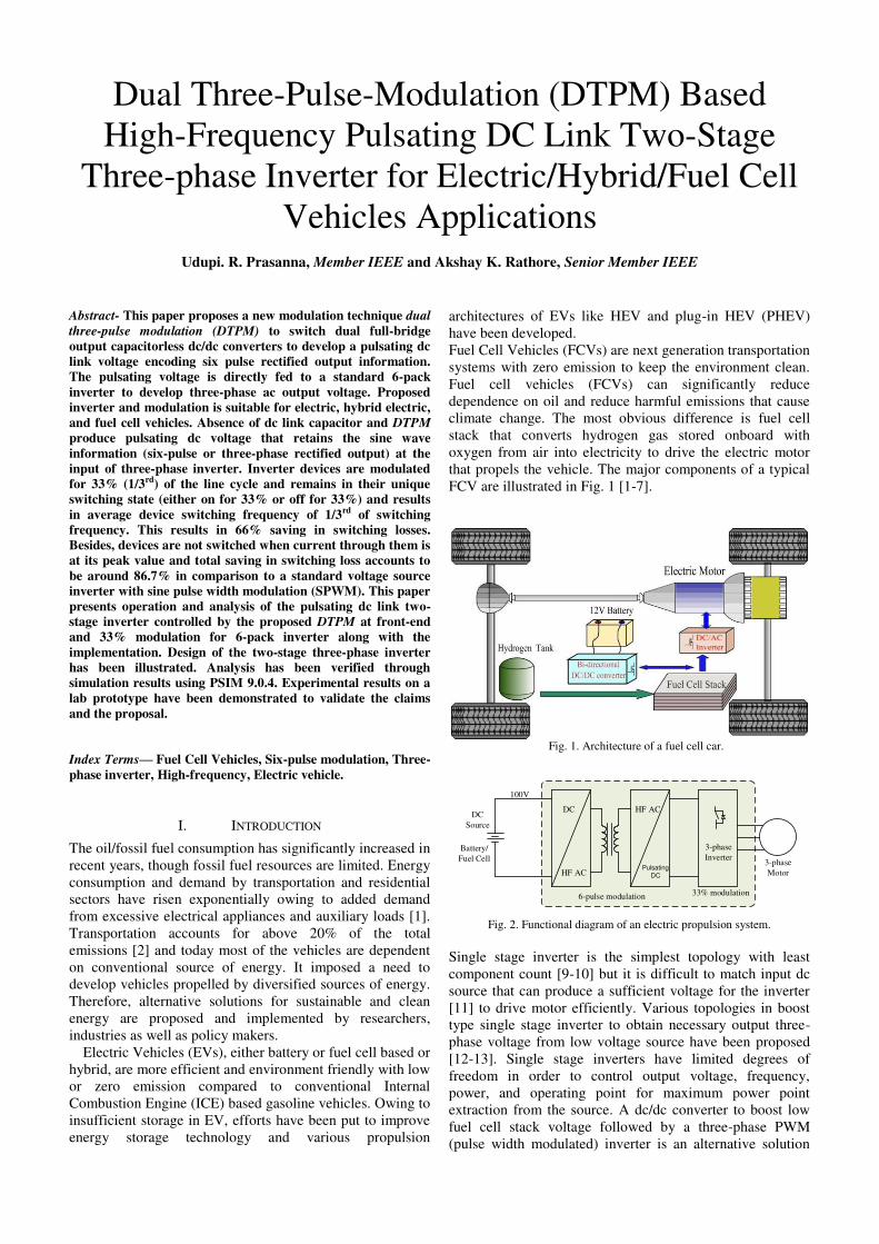
Fuel Cell Vehicles (FCVs) are next generation transportation
systems with zero emission to keep the environment clean.
Fuel cell vehicles (FCVs) can significantly reduce
dependence on oil and reduce harmful emissions that cause
climate change. The most obvious difference is fuel cell
stack that converts hydrogen gas stored onboard with
oxygen from air into electricity to drive the electric motor
that propels the vehicle. The major components of a typical
FCV are illustrated in Fig. 1 [1-7].
Fig. 1. Architecture of a fuel cell car.
3-phase
Inverter
DC
HF AC
HF AC
Pulsating
DC
6-pulse modulation 33% modulation
DC
Source
100V
3-phase
Motor
Battery/
Fuel Cell
Fig. 2. Functional diagram of an electric propulsion system.
Single stage inverter is the simplest topology with least
component count [9-10] but it is difficult to match input dc
source that can produce a sufficient voltage for the inverter
[11] to drive motor efficiently. Various topologies in boost
type single stage inverter to obtain necessary output three-
phase voltage from low voltage source have been proposed
[12-13]. Single stage inverters have limited degrees of
freedom in order to control output voltage, frequency,
power, and operating point for maximum power point
extraction from the source. A dc/dc converter to boost low
fuel cell stack voltage followed by a three-phase PWM
(pulse width modulated) inverter is an alternative solution
2168-6777 (c) 2013 IEEE. Personal use is permitted, but republication/redistribution requires IEEE permission. Seehttp://www.ieee.org/publications_standards/publications/rights/index.html for more information.
This article has been accepted for publication in a future issue of this journal, but has not been fully edited. Content may change prior to final publication. Citation information: DOI10.1109/JESTPE.2014.2304472, IEEE Journal of Emerging and Selected Topics in Power Electronics
but has lower efficiency. In order to reduce the switching
losses and improve efficiency, various soft-switching
methods have been proposed [14-17]. This paper proposes a
two-stage inverter with pulsating dc link shown in Fig. 2
with two-reference DTPM to control front-end converter and
33% modulation to control next stage 6-pack inverter to
produce three-phase output. DTPM at front-end produces
pulsating dc voltage that contains encoded six pulse three-
phase rectified sine information. In next stage, 33%
modulation for 6-pack inverter develops required three-
phase output with 66% reduction in commutations. Dc bus
of 100-110 V is derived either from fuel cell or battery.
Though a hybrid modulation technique for inverter control
has been proposed earlier [18-19], the front-end dc/dc
conversion has higher number of semiconductor devices
(one additional full-bridge due to individual three-phase
SPWM to each bridge) having multiple references with
complex control and modulation does not account for
variation in dc link voltage. Authors have reported this
technique in [20]. This paper is a revised version with
detailed analysis of modulation, loss modeling, enhanced
simulation results and additional experimental results.
Inverter operation during regenerative braking is similar to
conventional modulation in reverse direction. Three-phase
inverter devices (S1 to S6) operate in PFC active rectifier
mode and the reverse current is guided to battery by gating
the devices on secondary side (S1a-S4a and S1b to S4b) of
front-end converter. Front-end devices (M1a-M4a and M1b to
M4b) are uncontrolled and their body diodes work as full-
bridge rectifier.
Advantage of this topology is that there will not be
overshoot in the dc link voltage due to absence of energy
storing element as compared with the conventional two-
stage converter. In conventional two-stage converter, the
regenerative energy is transferred from traction drive to the
dc link and from dc link back to the dc source. However in
the proposed topology, absence of dc link capacitor reduces
the number of effective stage to one by transferring energy
directly to the input dc source.
The overall two-stage three-phase inverter system has the
following features: (a) Elimination of dc link electrolytic
capacitor that reduces the size and volume of system, (b)
only one pair out of three pairs of 6-pack inverter is being
switched at high frequency keeping other two pairs at same
switching state. This significantly reduces switching losses
and improves efficiency, (c) switching losses are further
more reduced because devices are not switched when current
is at its peak, (d) two references are used to implement
DTPM and are derived from three phase references, e)
objective is achieved with front-end bridges (instead of
three). It reduces the number of devices, volume, and cost
significantly when interleaved for high power. In the
proposed topology and modulation/control, the overall
converter has to be considered as a single unit and the two
stages function in synchronism. Elimination of dc link
capacitor reduces the order of the system, since link voltage
is not a state variable anymore. The proposed converter is
controlled like an ‘unfolding inverter’ where the modulation of ‘front-end’ stage and ‘last stage’ are synchronized. It will not introduce additional harmonic issues.
The objectives of this paper are to present operation and
analysis of the inverter system for the proposed modulation
scheme, which have been reported in Section II. Design of
the converter has been illustrated in Section III. Analysis and
design have been verified by simulation results using PSIM
9.0 in Section IV. Experimental results on a laboratory
prototype of 400W are demonstrated in Section IV to
validate the proposed modulation scheme.
II. OPERATION AND ANALYSIS OF THE CONVERTER
In this Section, steady-state operation and analysis of two-
stage three-phase inverter with proposed modulation have
been studied and discussed. Two full-bridge converters are
connected in parallel at front-end and series output fashion
as shown in Fig. 3 without dc link capacitor. Dual front-end
bridges are modulated using two reference signals VA,ref and
VB,ref to produce pulsating dc voltage Vdc at the output of
diode bridge rectifier. Unipolar pulsating dc voltage is fed
directly to a standard 6-pack three-phase inverter, which is
modulated to generate desired balanced three-phase ac
output. Front-end DTPM produces pulsating dc voltage that
contains encoded six pulse three-phase rectified sine
information. Once the pulsating dc voltage is processed by
6-pack inverter devices with 33% modulation of inverter
devices, output is filtered to obtained balanced three-phase
sine voltages of desired frequency and amplitude.
Lmb
1:n
HF Tr
C
D
M4a
Lma
1:n
HF Tr S2a
CF
S1a
S3a
S4a
D4a
C4a
Vin
Cin
M2a
D2a
C2a
iin
A
B
LF
S2
S1 S3
S4
+
-
Va
Vb
+
-
+
-VRa
iina
iinb
M1b
D1b
M3b
D3b
C3b
M1a
D1a
C1aM3a
D3a
C3a
S5
S6
S2b
S1b
S3b
S4b
VRb
+
-
Vdc
3-phase
load
C1b
M2b M4b
D2b D4b
C2b C4b
UV W
ipri,a
ipri,b
im,a
im,b
idcisec,a
isec,b
X
Y
Z
N
Cell-A
Cell-B
+
-
DR1a
DR2a
DR3a
DR4a
DR1b DR3b
DR2b DR4b
Fig. 3. Schematic of the proposed fuel cell inverter system.
2168-6777 (c) 2013 IEEE. Personal use is permitted, but republication/redistribution requires IEEE permission. Seehttp://www.ieee.org/publications_standards/publications/rights/index.html for more information.
This article has been accepted for publication in a future issue of this journal, but has not been fully edited. Content may change prior to final publication. Citation information: DOI10.1109/JESTPE.2014.2304472, IEEE Journal of Emerging and Selected Topics in Power Electronics
The following assumptions are made to study the operation
and analysis of the inverter: 1) All semiconductor devices
are ideal. 2) Leakage inductance of the transformers has
been neglected. 3) Dc/dc converter cells are identical and
modulated at higher frequency compared to the inverter.
Hence, current drawn by the inverter, idc remains
approximately constant over one switching cycle of dc/dc
converter. 4) All the components are ideal and lossless.
A. Modulation
The device pairs M1a - M2a and M3a - M4a are operated in
complementary fashion with each device conducting for half
of the switching cycle. Gating signals of M1a and M3a are
phase shifted by DTs, where D is duty ratio of the full-bridge
devices. By varying duty ratio, voltage across rectifier
output can be varied linearly. In the proposed modulation
scheme, the duty ratio Da for cell-A is generated from VA,ref.
Similarly duty ratio Db of cell-B is generated from VB,ref .
Reference signals VA,ref and VB,ref are three-pulse waveforms
for DTPM shown in Fig. 4 developed from three-phase
voltages while keeping in mind six-pulse waveform of three-
phase rectified output signal. In other words, a six-pulse
waveform has been divided into two three-pulse waveforms.
At the rectifiers’ output, the three-pulse voltages from each
rectifier are added up to obtain resultant VA,ref - VB,ref output,
which is six-pulse waveform on an average Vdc,avg as shown
in Fig. 4. As the name suggests, the frequency of six-pulse
rectifier output (pulsating dc voltage) has 6x the line
frequency. These six equal segments are flagged as T1 ~ T6. During each of these intervals, only one out of three legs of
the 6-pack inverter is modulated at high frequency. Whereas
remaining two inverter legs retain their unique switching
state. The modulating sequences for the 6-pack inverter
devices S1 ~ S6 are given in Table I and are compared with
common carrier waveform to get triggering pulses for the
devices. During time interval T1, S4 and S5 are operating in
on-state, S3 and S6 are in off-state, and only S1 and S2 are
modulated at high frequency using Vab/Vcb as modulating or
reference signal. It should be observed from Fig. 5 that only
two (one leg) of six devices (3 legs) are switched at high
frequency resulting. Two legs retain their current switching
state. Similar procedure is followed for the remaining five
segments in a line cycle. It means, in a line cycle, each
semiconductor device is switched at high frequency only for
1/3rd
of the time period (33%). It is also important to note
that devices do not commutate at their peak current. This
further reduces the switching losses. The modulation shown
in Table I results in improved THD value of output
waveform as compared to previous method given in [18-20]
that gives unsymmetrical wave shape. In proposed method,
exact modulating signals are calculated by considering
variation in average dc link voltage in six pulse fashion.
This modulation technique is simple and easy to implement
by using three phase voltages Van, Vbn, and Vcn as references
as shown in Fig. 6. VA,ref and VB,ref are obtained from these
three references as in Table. I. These references along with
carrier waveform generate gating signals for switches M1a -
M4a of cell-A as well as for M1b - M4b of cell-B. Modulation
scheme given in Table I is implemented for inverter devices
by selecting modulating signal in the given sequence.
0.4
0.6
0.8
1
VA
, re
f
-1
-0.8
-0.6
VB
,ref
0.01 0.0133 0.0166 0.02 0.0233 0.0266 0.031.4
1.5
1.6
1.7
Time
Vd
c,a
vg
Fig. 4. Modulating waveforms VA,ref and VB,ref for the proposed interleaved converter
topology and average voltage obtained at dc-link, Vdc,avg .
1.4
1.6
Vre
f
0
1.5
0
1
S1
0
1
S3
0 0.005 0.01 0.015 0.02 0.025
0
1
Time
S5
mod-A
mod-B mod-C
Fig. 5. Modulating waveforms for the proposed converter-inverter topology as shown
in Fig. 3.
Vab,ref
Vbc,ref
Vca,ref
Carrier
VA,ref Gate Signal to
Cell-A Switches
-1
abcb
bc
ac
ba
MUX-1
-1
Counter
Modulator
Carrier
1 0
S1
S2
S3
S4
S5
S6
Modulator
ca
MUX
MUX
Carrier
VB,ref Gate Signal to
Cell-B SwitchesModulator
bnbn
cn
cn
an
an
cnan
an
bn
cn
bn
+
-+
-+
-
Van,ref
Vbn,ref
Vcn,ref
÷
+ -
Fig.6. Schematic of complete modulation implementation.
Table. I. Modulation signals for switching of converters and inverter.
T1 T2 T3 T4 T5 T6
VA,ref Vcn Van Van Vbn Vbn Vcn
VB,ref Vbn Vbn Vcn Vcn Van Van
1S ,2S Vab/Vcb 1 1 Vac/Vbc 0 0
3S ,4S 0 0 Vbc/Vac 1 1 Vba/Vca
5S ,6S 1 Vcb/Vab 0 0 Vca/Vba 1
B. Steady State Operation
The converter operation during different intervals of a high-
frequency (HF) switching cycle is highlighted using steady-
state operating waveforms shown in Fig. 7. Gating signals of
front-end dual full-bridges converter are presented, where
each switch is operated with 50% duty ratio and
complementary to another switch in the same leg. Whenever
2168-6777 (c) 2013 IEEE. Personal use is permitted, but republication/redistribution requires IEEE permission. Seehttp://www.ieee.org/publications_standards/publications/rights/index.html for more information.
This article has been accepted for publication in a future issue of this journal, but has not been fully edited. Content may change prior to final publication. Citation information: DOI10.1109/JESTPE.2014.2304472, IEEE Journal of Emerging and Selected Topics in Power Electronics
the diagonal switch pairs are turned-on, say M1a and M4a, an
input voltage appears across the primary of the transformer
and corresponding voltage is reflected on secondary side. On
the other hand, other diagonal pair M2a and M3a is
conducting, negative voltage (-n*Vin) is obtained across
secondary terminals, where n is the turns ratio of the
transformer. Another converter cell is also operated in
similar manner applying gating pulses of different duty ratio
Db which is being generated from VB,ref. Bipolar pulsating
voltage is converted to unipolar using diode bridge rectifier.
Average value of voltage output at the full bridge converter
is obtained as,
inaRa VnDV 2 (1)
inbRb VnDV 2 (2) inbaRbRadc VnDDVVV 2
(3)
Where Da and Db are duty ratios of cell-A and cell-B,
respectively, which vary between 0 and 0.5.
Va
Vdc
Im,a
Ts/2DaTs Ts/2
nVin
-nVin
nVin
-nVin
nVinVRa
2nVin
nVin
Isec,a
Ipri,a
Idc
-Idc
Idc
-Idc
Vb nVin
-nVin
nVin
-nVin
nVinVRb
nVin
Im,b
Isec,bIdc
-Idc
Idc
-Idc
Ipri,b
DbTs
Fig. 7. Waveforms showing gating signals, voltage and current at essential parts of the
full-bridge converter.
VB, ref represented in Fig. 4, Fig. 6 and Fig. 9a corresponds to
reference signal that is used to generate gate signals for cell-
B. Modulator for cell-B shown in Fig. 6 inverts this voltage
reference to generate duty cycle. Six pulse reference Vdc,avg is
obtained by VA,ref - VB, ref. Since two cells are connected in
series at dc link, it turns out to be Vdc=VRa+VRb. Inversion of
cell-B voltage is done at the modulator.
Duty ratio of the two cells Da and Db are generated from
VA,ref and VB,ref respectively. Duty ratio varies between
maximum value Dmax and minimum value Dmin as the VA,ref
and VB,ref vary at 150 Hz (3x line frequency). Maximum
value of voltage obtained at Vdc corresponds to peak of line
to line inverter output voltage is obtained at (Da +Db)max.
Hence the output voltage is obtained as, inbapeakXY VnDDV max, 4 (4)
Where, VXY,peak is the peak of line-line output voltage. Output
voltage is varied by varying the reference voltage Vref, which
changes the range of operating duty ratios Dmin and Dmax.
C. Switching losses
From the explanation given above, it is clear that devices of
the three phase inverter switch at high frequency only for
one third of the cycle. Switch is kept in on-state for one third
of the cycle conducting peak current of output line current
when output power factor is unity. Devices are modulated at
high frequency when the line current crosses zero. Total
switching loss in the inverter Psw,DTPM can be analytically
calculated as,
12
12
,6
16S
S
T
T
SIOFFONXDC
S
DTPMsw dtfttiVT
P
12
7
12
5 6
1S
S
T
T
SIOFFONXDC dtfttiV (5)
2
31
2, SIOFFONXDCDTPMsw fttIVP
(6)
Where, TS is the time period of three phase output voltage,
VDC is dc link voltage during switching which is equal to
4n*Vin, iX is the output line current given by IX*sin(ωt) , tON
and tOFF are switching on-time and switching off-time of the
switch and fSI is the inverter switching frequency.
Switching losses for standard sine PWM, Psw,PWM are
calculated in similar fashion where all the six devices are
switched at high frequency.
ST
SIOFFONXDC
S
PWMsw dtfttiVT
P0
,6
116
(7)
SIOFFONXDCPWMsw fttIVP 2
,
(8)
Reduction is switching losses is obtained from (6) and (8),
134.02
31
,
,
PWMsw
DTPMsw
P
P
(9)
Switching losses in the inverter devices reduce by around
7.5 times by the proposed modulation as compared to
standard sine pulse width modulation (SPWM).
Similarly, switching losses are calculated for varying load
power factor by substituting output current as IX*sin(ωt+φ) and their ratio owing to DTPM and SPWM is given in (10).
6
66
;2
sin
;cos2
31
,
,
PWMsw
DTPMsw
P
P
(10)
It is observed from Fig. 8 that reduction in switching losses
is more than 50% for any given load power factor varying
from lagging to leading and is maximum of 86.6% at unity
power factor.
2168-6777 (c) 2013 IEEE. Personal use is permitted, but republication/redistribution requires IEEE permission. Seehttp://www.ieee.org/publications_standards/publications/rights/index.html for more information.
This article has been accepted for publication in a future issue of this journal, but has not been fully edited. Content may change prior to final publication. Citation information: DOI10.1109/JESTPE.2014.2304472, IEEE Journal of Emerging and Selected Topics in Power Electronics
-1 -0.8 -0.6 -0.4 -0.2 0 0.2 0.4 0.6 0.8 10.1
0.15
0.2
0.25
0.3
0.35
0.4
0.45
0.5
Power Factor
Sw
itch
ing L
oss
SP
M/P
WM
Fig. 8. Reduction in switching losses with DTPM compared to SPWM for
different load power factor.
III. DESIGN OF THE CONVERTER
In this Section, design procedure is illustrated by a design
example with a converter of following specifications: Input
voltage Vin = 100 V, output phase voltage VO = 110 V rms at
frequency fO = 50 Hz, output power Po = 400 W, switching
frequency of front-end dc/dc converters fSC = 100 kHz and 6-
pack switching frequency of inverter fSI = 40 kHz.
(1) Average input current is Iin = Po/(ηVin). Assuming an
efficiency η of nearly 95%, Iin = 4.21 A. Each converter cell
is sharing half of load, Iina = Iinb = Iin /2 = 2.1A.
(2) Maximum value of average dc link voltage of the
inverter is
27023 odc VV (11)
(3) Transformers’ turns ratio is designed by considering operating duty ratio of full-bridge converter as 0.4 to 0.425.
From (3), value of turns ratio n is calculated as,
inba
dc
VDD
Vn
max2 (12)
Turns ratio of 1.84 is obtained considering (Da +Db)max as
3425.0 .
(4) Rating of full-bridge converter: Switches M1a- M4a and
M1b- M4b are rated for Iina = Iinb = 2.1A and rated to withstand
voltage of Vin =100V.
(5) Rectifier diodes should block a voltage of nVin and
average current of Idc given by,
min,dc
Odc
V
PI
(13)
Here, Idc ≈ 1.71 A. Voltage rating of rectifier diodes, VDR
= nVin ≈ 200 V.
(6) Inverter: Voltage rating of the inverter switches is
selected based on the maximum voltage across dc link,
which is equal to 2n times the input voltage. RMS current
rating of the switches is same as output current IO.
For the given specifications, voltage rating is equal to 400V
and current rating is 1.71A.
(7) Filter design: Filter inductor is calculated such that
voltage drop across the inductor is less than 2% of the
nominal voltage at full load condition.
OO
OF
If
VL
202.0
(14)
Where, fO and IO are the output frequency and output
current. For the given specifications, its value is obtained as
10 mH. Filter capacitor is decided according to the cut-off
frequency of the low pass filter. For this application, 10% of
the converter switching frequency fSC is selected as the cut-
off frequency. Filter capacitor is calculated as,
FC
FLf
C 224
1
(15)
Where, fC is the cut-off frequency of the filter. For fC=4 kHz,
capacitor CF is obtained as 0.16µF.
IV. SIMULATION AND EXPERIMENTAL RESULTS
The proposed modulation has been implemented and
simulated for two-stage inverter using software package
PSIM 9.0. Simulation results are illustrated in Fig. 9 to Fig.
11. The results coincide closely with the predicted operating
waveforms.
Fig. 9a shows waveforms of reference signal VA,ref and VB,ref,
which are used to obtain gating pulses for the full-bridge
converters. The two references are attained by selecting
signals from three-phase voltages Van, Vbn and Vcn as given in
Table I. References for 6-pack inverter modulation are
derived by comparing modA, modB and modC waveforms
shown in Fig. 9b with the carrier signal of 40 kHz. For 33%
of the line cycle, top switch of one leg remains on, bottom
switch gets on state for other 33%, and the devices of the leg
are modulated at high frequency for rest 33% of the line
cycle. It contributes to low switching losses. It is also
observed that only one of the legs is switching at high
frequency, remaining two device legs being connected to
either Vdc or 0. In order to generate pulsating dc voltage at
Vdc, semiconductor devices are switched with varying duty
ratio generated from two reference signals, VA,ref and VB,ref
Fig. 9. Simulation waveforms showing modulating signals (a) VA,ref and
VB,ref for full-bridge converters cell-A and cell-B, (b) modA, modB and
modC for three-phase inverter legs
2168-6777 (c) 2013 IEEE. Personal use is permitted, but republication/redistribution requires IEEE permission. Seehttp://www.ieee.org/publications_standards/publications/rights/index.html for more information.
This article has been accepted for publication in a future issue of this journal, but has not been fully edited. Content may change prior to final publication. Citation information: DOI10.1109/JESTPE.2014.2304472, IEEE Journal of Emerging and Selected Topics in Power Electronics
Fig. 13. Experimental waveforms showing gate signals to inverter top
switches demonstrating 33% modulation (X-axis: 5ms/div and Y-axis:
10V/div).
Fig. 14. Experimental waveforms of three phase output voltages (X-axis:
5ms/div, Y-axis: 100V/div).
2168-6777 (c) 2013 IEEE. Personal use is permitted, but republication/redistribution requires IEEE permission. Seehttp://www.ieee.org/publications_standards/publications/rights/index.html for more information.
This article has been accepted for publication in a future issue of this journal, but has not been fully edited. Content may change prior to final publication. Citation information: DOI10.1109/JESTPE.2014.2304472, IEEE Journal of Emerging and Selected Topics in Power Electronics
Fig. 15. Experimental result showing of three phase output currents (top,
scale: 0.5A/div) along with the line-line voltage (bottom, scale: 100V/div)
(X-axis: 5ms/div).
Fig. 16. Experimental waveform showing gate voltage of switch S1 VGS,1
(top, scale: 20V/div) and voltage across it VDS,1 (bottom, scale: 200V/div)
(X-axis: 5ms/div).
Fig. 17. Experimental waveforms of voltage across primary of the
transformer of cell-A and cell-B, VAB and VCD (scale: 200V/div), and voltage
input to the inverter Vdc (scale: 100V/div).
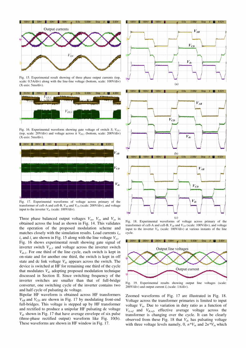
Three phase balanced output voltages Vxn, Vyn and Vzn is
obtained across the load as shown in Fig. 14. This validates
the operation of the proposed modulation scheme and
matches closely with the simulation results. Load currents ix,
iy and iz are shown in Fig. 15 along with the line voltage Vxy.
Fig. 16 shows experimental result showing gate signal of
inverter switch Vgs,1 and voltage across the inverter switch
Vds,1. For one third of the line cycle, each switch is kept in
on-state and for another one third, the switch is kept in off
state and dc link voltage Vdc appears across the switch. The
device is switched at HF for remaining one third of the cycle
that modulates Vdc adopting proposed modulation technique
discussed in Section II. Since switching frequency of the
inverter switches are smaller than that of full-bridge
converter, one switching cycle of the inverter contains two
and half cycle of pulsating dc voltage.
Bipolar HF waveform is obtained across HF transformers
VAB and VCD are shown in Fig. 17 by modulating front-end
full-bridges. This voltage is stepped up by HF transformer
and rectified to produce a unipolar HF pulsating dc voltage
Vdc shown in Fig. 17 that have average envelope of six pulse
(three-phase rectified output) waveform like Fig. 10(b).
These waveforms are shown in HF window in Fig. 17.
(a)
(b)
(c)
Fig. 18. Experimental waveforms of voltage across primary of the
transformer of cell-A and cell-B, VAB and VCD (scale: 100V/div), and voltage
input to the inverter Vdc (scale: 100V/div) at various instants of the line
cycle.
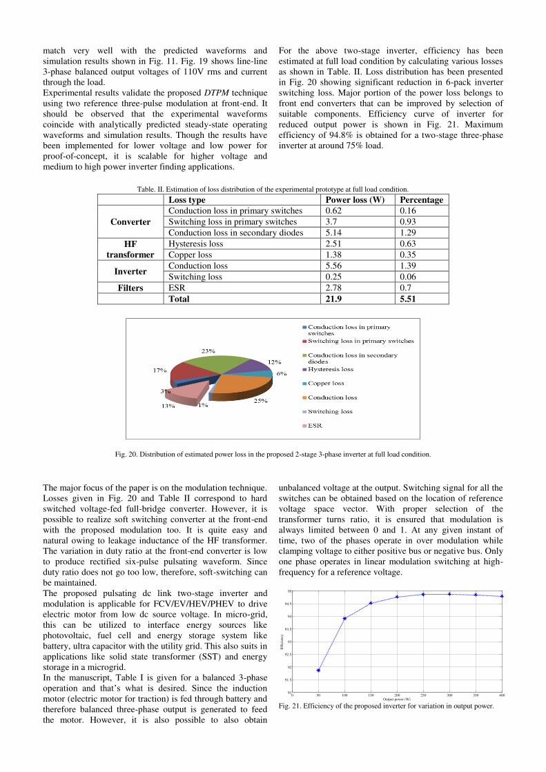
Fig. 19. Experimental results showing output line voltages (scale:
200V/div) and output current Io (scale: 1A/div).
Zoomed waveforms of Fig. 17 are illustrated in Fig. 18.
Voltage across the transformer primaries is limited to input
voltage Vin. Due to variation in duty ratio as a function of
VA,ref and VB,ref, effective average voltage across the
transformer is changing over the cycle. It can be clearly
observed from these Fig. 18 that Vdc has pulsating voltage
with three voltage levels namely, 0, n*Vin and 2n*Vin which
2168-6777 (c) 2013 IEEE. Personal use is permitted, but republication/redistribution requires IEEE permission. Seehttp://www.ieee.org/publications_standards/publications/rights/index.html for more information.
This article has been accepted for publication in a future issue of this journal, but has not been fully edited. Content may change prior to final publication. Citation information: DOI10.1109/JESTPE.2014.2304472, IEEE Journal of Emerging and Selected Topics in Power Electronics
match very well with the predicted waveforms and
simulation results shown in Fig. 11. Fig. 19 shows line-line
3-phase balanced output voltages of 110V rms and current
through the load.
Experimental results validate the proposed DTPM technique
using two reference three-pulse modulation at front-end. It
should be observed that the experimental waveforms
coincide with analytically predicted steady-state operating
waveforms and simulation results. Though the results have
been implemented for lower voltage and low power for
proof-of-concept, it is scalable for higher voltage and
medium to high power inverter finding applications.
For the above two-stage inverter, efficiency has been
estimated at full load condition by calculating various losses
as shown in Table. II. Loss distribution has been presented
in Fig. 20 showing significant reduction in 6-pack inverter
switching loss. Major portion of the power loss belongs to
front end converters that can be improved by selection of
suitable components. Efficiency curve of inverter for
reduced output power is shown in Fig. 21. Maximum
efficiency of 94.8% is obtained for a two-stage three-phase
inverter at around 75% load.
Table. II. Estimation of loss distribution of the experimental prototype at full load condition.
Loss type Power loss (W) Percentage
Converter
Conduction loss in primary switches 0.62 0.16
Switching loss in primary switches 3.7 0.93
Conduction loss in secondary diodes 5.14 1.29
HF
transformer
Hysteresis loss 2.51 0.63
Copper loss 1.38 0.35
Inverter Conduction loss 5.56 1.39
Switching loss 0.25 0.06
Filters ESR 2.78 0.7
Total 21.9 5.51
Fig. 20. Distribution of estimated power loss in the proposed 2-stage 3-phase inverter at full load condition.
The major focus of the paper is on the modulation technique.
Losses given in Fig. 20 and Table II correspond to hard
switched voltage-fed full-bridge converter. However, it is
possible to realize soft switching converter at the front-end
with the proposed modulation too. It is quite easy and
natural owing to leakage inductance of the HF transformer.
The variation in duty ratio at the front-end converter is low
to produce rectified six-pulse pulsating waveform. Since
duty ratio does not go too low, therefore, soft-switching can
be maintained.
The proposed pulsating dc link two-stage inverter and
modulation is applicable for FCV/EV/HEV/PHEV to drive
electric motor from low dc source voltage. In micro-grid,
this can be utilized to interface energy sources like
photovoltaic, fuel cell and energy storage system like
battery, ultra capacitor with the utility grid. This also suits in
applications like solid state transformer (SST) and energy
storage in a microgrid.
In the manuscript, Table I is given for a balanced 3-phase
operation and that’s what is desired. Since the induction motor (electric motor for traction) is fed through battery and
therefore balanced three-phase output is generated to feed
the motor. However, it is also possible to also obtain
unbalanced voltage at the output. Switching signal for all the
switches can be obtained based on the location of reference
voltage space vector. With proper selection of the
transformer turns ratio, it is ensured that modulation is
always limited between 0 and 1. At any given instant of
time, two of the phases operate in over modulation while
clamping voltage to either positive bus or negative bus. Only
one phase operates in linear modulation switching at high-
frequency for a reference voltage.
0 50 100 150 200 250 300 350 40091
91.5
92
92.5
93
93.5
94
94.5
95
Output power (W)
Eff
icie
ncy
Fig. 21. Efficiency of the proposed inverter for variation in output power.
2168-6777 (c) 2013 IEEE. Personal use is permitted, but republication/redistribution requires IEEE permission. Seehttp://www.ieee.org/publications_standards/publications/rights/index.html for more information.
This article has been accepted for publication in a future issue of this journal, but has not been fully edited. Content may change prior to final publication. Citation information: DOI10.1109/JESTPE.2014.2304472, IEEE Journal of Emerging and Selected Topics in Power Electronics
V. SUMMARY AND CONCLUSION
EVs/HEVs/FCVs are low or zero emission transportation
systems offering clean mobility owing to no combustion of
oil and gas. Compact, lightweight, and high efficiency
power electronics system is expected as a part of electric
propulsion system. This paper proposes a two-stage three-
phase inverter with pulsating dc link and novel modulation
technique to control dual full-bridges at front-end to develop
pulsating dc link followed by a 33% modulation to standard
6-pack inverter.
In the proposed topology and modulation, the overall
inverter has to be considered as a single unit and the two
stages function in synchronism. Elimination of the link
capacitance reduces the order of the system. The proposed
converter is controlled like an ‘unfolding inverter’ where the modulations of ‘front-end’ and ‘last stage’ are synchronized.
It will not introduce additional harmonic issues.
A two reference modulation for dual full-bridges at front end
has been proposed to produce high-frequency pulsating dc
voltage. The proposed modulation eliminates dc-link
capacitor and directly feeds pulsating dc voltage to next 6-
pack inverter. The pulsating dc link voltage contains
encoded six pulse three-phase rectified sine information.
This pulsating dc waveform is utilized to generate three-
phase output voltage achieving significant reduction in
switching losses of the inverter. Switching states of the 6-
pack inverter devices are modulated at high-frequency for
33% of the line cycle, while remains in unique steady-state
for rest of the line cycle. Average inverter device switching
frequency over a line cycle is 1/3rd
of the switching
frequency. Compared to standard voltage source inverter
(VSI) modulated by traditional carrier based SPWM,
reduction in switching loss of approximately 86.7% of 6-
pack inverter is accomplished.
Steady-state operation and analysis of the two-stage inverter
with proposed modulation technique has been explained.
Simulation waveforms are obtained using PSIM 9.0.4 and
verify the proposed operation and modulation at steady-
state. Experimental results demonstrate the accuracy and
effectiveness of the claims and proposal. The proposed
system is suitable for driving the motor (vehicle) with low
voltage battery bank.
REFERENCES
[1] A. Emadi, and S. S. Williamson, “Fuel cell vehicles: opportunities and challenges,” IEEE PES meeting 2004, pp. 1640-1645.
[2] S. Aso, M. Kizaki, and Y. Nonobe, “Development of hybrid fuel cell vehicles in Toyota,” in Proc. IEEE PCC 2007, pp. 1606-1611.
[3] K. Rajashekhara, “Power conversion and control strategies for fuel cell vehicles,” in Proc. IEEE IECON 2003, 2865-2870.
[4] A. Emadi, S. S. Williamson, and A. Khaligh, “Power electronics
intensive solutions for advanced electric, hybrid electric, and fuel cell
vehicular power systems,” IEEE Trans. on Power Electronics, pp.
567-577, 2006.
[5] A. Emadi, K. Rajashekara, S. S. Williamson, and S. M. Lukic,
“Topological overview of hybrid electric and fuel cell vehicular power system architectures and configurations” IEEE Trans. on Vehicular
Technology, pp. 763-770, 2005.
[6] A. Khaligh and Z. Li, “Battery, Ultracapacitor, Fuel Cell, and Hybrid
Energy Storage Systems for Electric, Hybrid Electric, Fuel Cell, and
Plug-In Hybrid Electric Vehicles: State of the Art,” IEEE Trans. on
Vehicular Technology, pp. 2806-2814, 2010.
[7] S. S. Williamson and A. Emadi, “Comparative assessment of hybrid electric and fuel cell vehicles based on comprehensive well-to-wheels
efficiency analysis”, IEEE Trans. on Vehicular Technology, vol. 54,
no. 3, pp. 856-862, May 2005.
[8] J. M. Miller, “Power electronics in hybrid electric vehicle applications,” in Proc. 18th IEEE Applied Power Electronics Conf.,
Miami Beach, FL, Feb. 2003, vol. 1, pp. 23-29.
[9] Y. Chen and K. Smedley, “A cost-effective single-stage inverter with
maximum power point tracking”, IEEE Trans. on Power Electronics,
vol. 19, no. 5, pp. 1289-1294, Sept. 2004.
[10] M. Jang, M. Ciobotaru and V. G. Agelidis, “A single-stage three-
phase fuel cell system based on a boost inverter with a battery back-up
unit”, in Proc. 27th IEEE Applied Power Electronics Conf., 2012, pp.
2032-2037.
[11] L. E. Lesster, “Fuel cell power electronics – managing a variable-
voltage dc source in a fixed-voltage ac world,” Fuel Cells Bulletin,
vol. 3, no. 25, 2000, pp. 5-9.
[12] Y. Chen and K. Smedley, “Three-phase boost-type grid-connected
inverter”, IEEE Trans. on Power Electronics, vol. 23, no. 5, Sept.
2008, pp. 2301-2309.
[13] C. Cecati, A. D. Aquila, and M. Liserre, “A novel three-phase single-
stage distributed power inverter”, IEEE Trans. on Power Electronics,
vol. 19, no. 5, pp. 1226-1233, Sept. 2004.
[14] D. M. Divan and G. Skibinski, “Zero-switching-loss for high-power
applications”, IEEE Trans. Industry Applications, vol. 25, no. 4, pp.
634-643, Jul./Aug. 1989.
[15] K. Rigbers, S. Thomas, U. Boke, and R. W. De Doncker, “Behavior and loss modeling of a three-phase resonant pole inverter operating
with 120o double flattop modulation”, in Proc. 41st Annual meeting
2168-6777 (c) 2013 IEEE. Personal use is permitted, but republication/redistribution requires IEEE permission. Seehttp://www.ieee.org/publications_standards/publications/rights/index.html for more information.
This article has been accepted for publication in a future issue of this journal, but has not been fully edited. Content may change prior to final publication. Citation information: DOI10.1109/JESTPE.2014.2304472, IEEE Journal of Emerging and Selected Topics in Power Electronics
Akshay Kumar Rathore
(M’05–SM’12) received the Master’s degree in electrical machines and drives from
Indian Institute of Technology
(BHU),Varanasi, India, in
2003. He received the Ph.D.
degree in power electronics
from University of Victoria,
Victoria, BC, Canada, in 2008.
He has two subsequent postdoctoral research appointments
with University of Wuppertal, Wuppertal, Germany from
Sep. 2008 to Aug. 2009 and University of Illinois, Chicago,
IL, USA, from Sep. 2009 to Sept. 2010.
Since Nov. 2010, he is currently an Assistant Professor with
the Department of Electrical and Computer Engineering,
National University of Singapore, Singapore. His research
interests mainly include analysis, design, and development
of current-fed converter technologies for renewable energy
and electric transportation applications, soft-switching
schemes and PWM modulation techniques for high
frequency power converters, and optimal low switching
frequency control of medium voltage multilevel inverters.
He has been actively researching on novel and innovative
soft-switching current-fed topologies and modulation
techniques. He has published 80 research papers in
international journals and conferences. He is an Associate
Editor of IEEE Transactions on Industry Applications and
IEEE Journal of Emerging Selected Topics in Power
Electronics. He is an Editor of Electric Power Components
and Systems. He has been a Guest Associate Editor for
special issue on transportation electrification and vehicle
systems in IEEE TRANSACTION ON POWER
ELECTRONICS, appeared on the December 2013 issue.
Dr. Rathore is a winner and recipient of 2013 IEEE IAS
Andrew W. Smith Outstanding Young Member Award. He
is the first working in Asia to receive this award. Dr.
Rathore has been listed in Marquis Who’s Who in Science and Engineering in 2006, Who’s Who in the World, and Who’s Who in America in 2008. He was awarded a Gold Medal for securing highest academic standing among all the
electrical engineering specializations during his Master’s degree study. He was a recipient of Ph.D. fellowship and
Thouvenelle Graduate Scholarship during his Ph.D. study.