39
Ductile to Brittle Transition (DBT) of a Single-Crystal 4H-SiC Wafer by Performing Nanometric Machining by Deepak Ravindra & John Patten
Ductile to Brittle Transition (DBT) of a Single-Crystal 4H-SiC Wafer by
Performing Nanometric Machining
byDeepak Ravindra & John Patten
Why Use Silicon Carbide?•Extreme hardness
•High wear resistance
•High thermal conductivity (3.4 W/cm.K )
•Wide energy bandgap (3.26eV)
•High electric field breakdown strength (2.22 x 10⁶ V/cm)•High maximum current density
•High saturated electron drift velocity (2 x 107 cm/sec)

Applications of 4H SiC•High-Frequency Power Devices
–RF & Microwave Amplifiers/Transmitters
•High-Temperature Devices–High temperature electronics & power devices
•Optoelectronic Devices–Laser diodes & photodiodes
•III-V Nitride Deposition–Light emitting devices

Ductile Regime Machining of SiC•Plastic flow of material in the form of severely sheared machining chips occur
•Possible due to High Pressure Phase Transformation (HPPT) or direct amorphization
•Plastic deformation caused from highly localized contact pressure and shear stresses.
•High pressure metallic phase could be used to improve manufacturing processes and ductile response during machining.
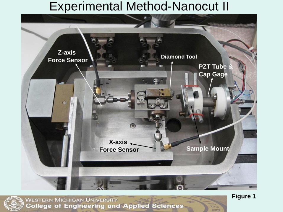
Experimental Method-Nanocut II
Figure 1
Diamond Tool
X-axis Force Sensor
Z-axis Force Sensor
Sample Mount
PZT Tube &Cap Gage
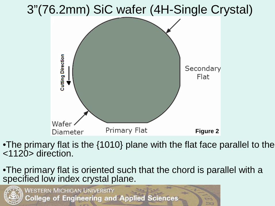
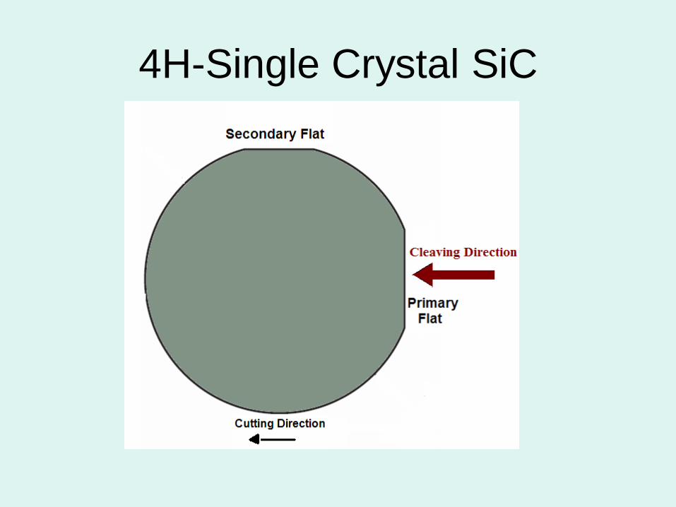
3”(76.2mm) SiC wafer (4H-Single Crystal)
•The primary flat is the {1010} plane with the flat face parallel to the <1120> direction.
•The primary flat is oriented such that the chord is parallel with a specified low index crystal plane.
Figure 2

Experimental Plan
•3 depth of cuts (100nm, 500nm & 1000nm) were planned to be carried out
•Predicted range of Ductile to Brittle Transition (DBT) is between 100nm – 1000nm
•A depth greater than 1000nm will only be carried out if the DBT is not identified with the first set of experiments.
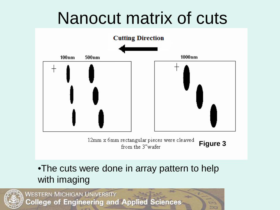
Nanocut matrix of cuts
•The cuts were done in array pattern to help with imaging
Figure 3

Results – Actual Cuts on SiC
•Cuts image under an optical microscope at 400x magnification
•Dimensions are approximately 10-20µm in length and 120µm in width
•Cutting direction from right to left
•The 10mm tool nose radius makes the cuts wider than they are longer
Cutting Direction
Figure 4

Results- Force Data
• Cutting and thrust forces increase as the depth of cut increases• Generally, beyond the DBT, the forces increase /decrease proportionally
lesser. • Due to lesser energy/force required to fracture material compared to ductile
response. • In this case, the brittle fracture was not so severe as to measurably affect
the resultant force trends
Figure 5

Results- Height Profile (Ductile)
•An AFM scanned section of a (1000nm programmed depth) cut.
•The measured depth is 816nm.
•The “V” shape of the ductile cut represents the imprint of the tool
Cutting Direction Figure 6
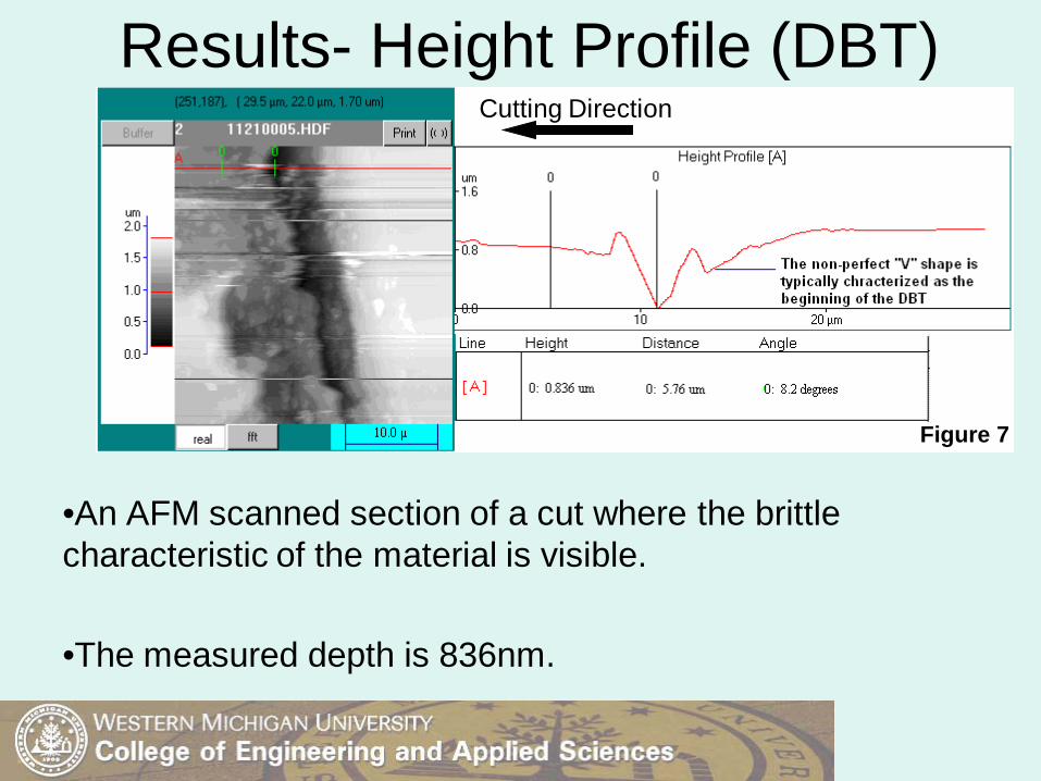
Results- Height Profile (DBT)
•An AFM scanned section of a cut where the brittle characteristic of the material is visible.
•The measured depth is 836nm.
Figure 7
Cutting Direction

Results- Height Profile (Brittle)
•An AFM scanned section of a cut where the brittle characteristic of the material is observed.
•The measured depth is 952nm.
•There could be more than one valley in the brittle region as the fracture process results in uncontrolled material removal.
Cutting Direction
Figure 8

Results- Height Profile (Brittle)
• The maximum measured depth of cut (1170nm) is more than the programmed depth of cut (1000nm).
• Due to microcracks that could extend deeper than the depth of cut below the machined surface
Cutting Direction
Figure 9

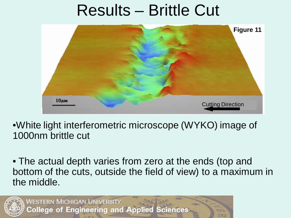
Results – Brittle Cut
•Optical image (200x) of 1000nm cut showing brittle fracture
• Jagged edges are due to crack propagation and uncontrolled material removalin the brittle regime.
Cutting Direction
Figure 10
Results – Brittle Cut
•White light interferometric microscope (WYKO) image of 1000nm brittle cut
• The actual depth varies from zero at the ends (top and bottom of the cuts, outside the field of view) to a maximum in the middle.
Cutting Direction
Figure 11

Ductile Nanometric Cutting
Brittle Nanometric Cutting
Well defined & straight edges Jagged edges & chipped material
Controlled material removal process
Hard to control as microcracks extend below the machined surface
Final depth of cut can be predicted below the DBT depth
No direct control of the resultant depth beyond the DBT depth
Good surface finish and mechanical properties
Poor surface finish and could end in a catastrophic failure at times

Using the DBT Information
• Precision Grinding-Design grits depth of penetration/chip load for abrasive wheels lesser than the DBT depth of the material
• Single Point Diamond Turning -Depth of cut at each pass should not exceed the DBT depth in order to prevent fracture

Conclusion•The DBT depth for a 4H-SiC wafer was determined to be between 820nm-830nm.
•Cutting forces and thrust forces increase as the depth of cut increases
•Beyond the DBT depth, the cut produced becomes brittle
•The fracture from brittle cutting then leads to pitting and microcracks, this results in significant and uncontrolled subsurface damage
• In order to machine a semiconductor or ceramic in the ductile-regime, it is crucial to know its DBT depth

Ongoing/Current Work1. Single Point Diamond Turning (SPDT) of CVD
coated SiC and other ceramics (i.e. Quartz).
2. Develop hybrid laser-SPDT machining process for smoothing ceramics.
Project Goals:– reduction in tool wear– increase in material removal rate– improvement in the final surface quality

Thank you

Nanocut Setup

Microscope to Locate Surface

Nanocut Stage

Nanocut DAQ System
4H-Single Crystal SiC
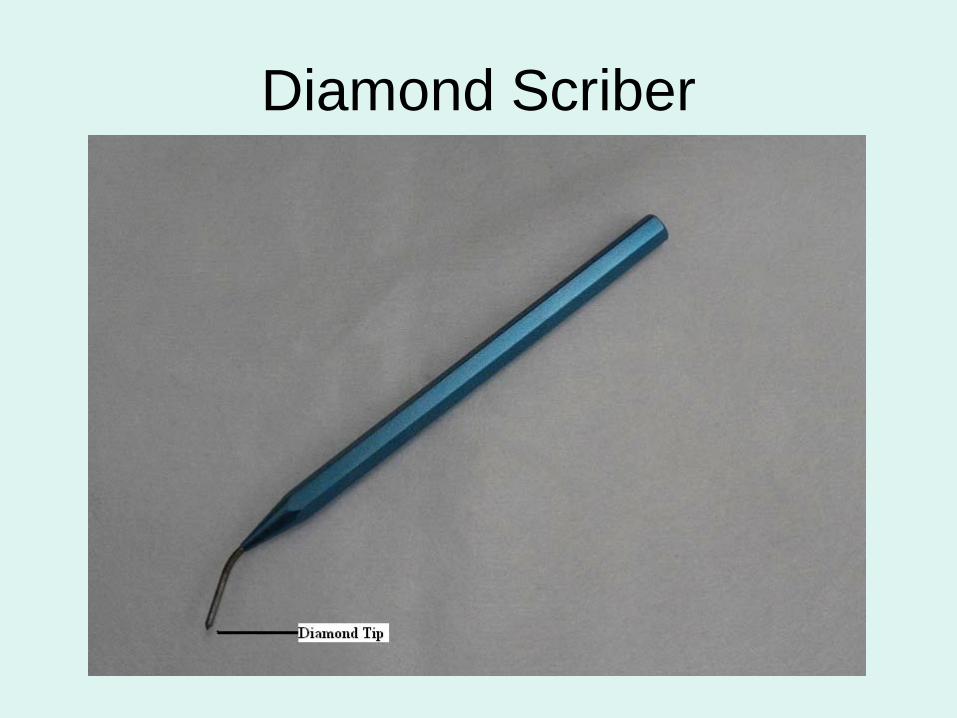
Diamond Scriber
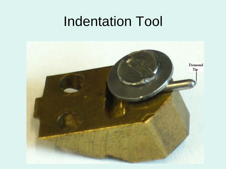
Indentation Tool

Single Point Diamond Tool
• Rake Angle = -45o
• Clearance Angle = 5o

Wide Energy Bandgap (3.26eV)
• Enables SiC to operate at extremely high temperatures without suffering from intrinsic conduction effects
• Allows SiC to emit and detect short wavelength light which makes the fabrication of blue light emitting diodes and nearly solar blind UV photodetectors possible.

High Breakdown Electric Field (2.22 x 10⁶ V/cm)
• Enables the fabrication of very high-voltage, high-power devices such as diodes, power transitors, power thyristors and surge suppressors, as well as high power microwave devices.
• Allows the devices to be placed very close together, providing high device packing density for integrated circuits.

High Thermal Conductivity (3.0-3.8 W/cm.K)
• At room temperature, SiC has a higher thermal conductivity than any metal.
• This property enables SiC devices to operate at extremely high power levels and still dissipate the large amounts of excess heat generated.

High Saturated Electron Drift Velocity (2.00 x 107 cm/sec)
• SiC devices can operate at high frequencies (RF and microwave) because of the high saturated electron drift velocity of SiC.
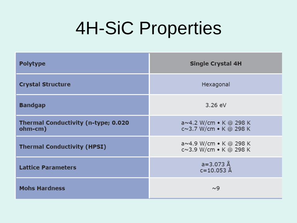
4H-SiC Properties

Surface Profile of Ductile Cut

Ductile Cut Surface Profile
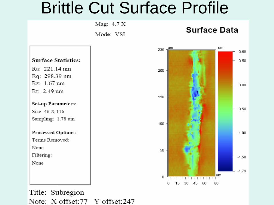
Brittle Cut Surface Profile

Precision Grinding SiC
•In order to avoid fracture/catastrophic failure:
Abrasive Grit Depth of Penetration < DBT Depth

SPDT of CVD coated SiC


