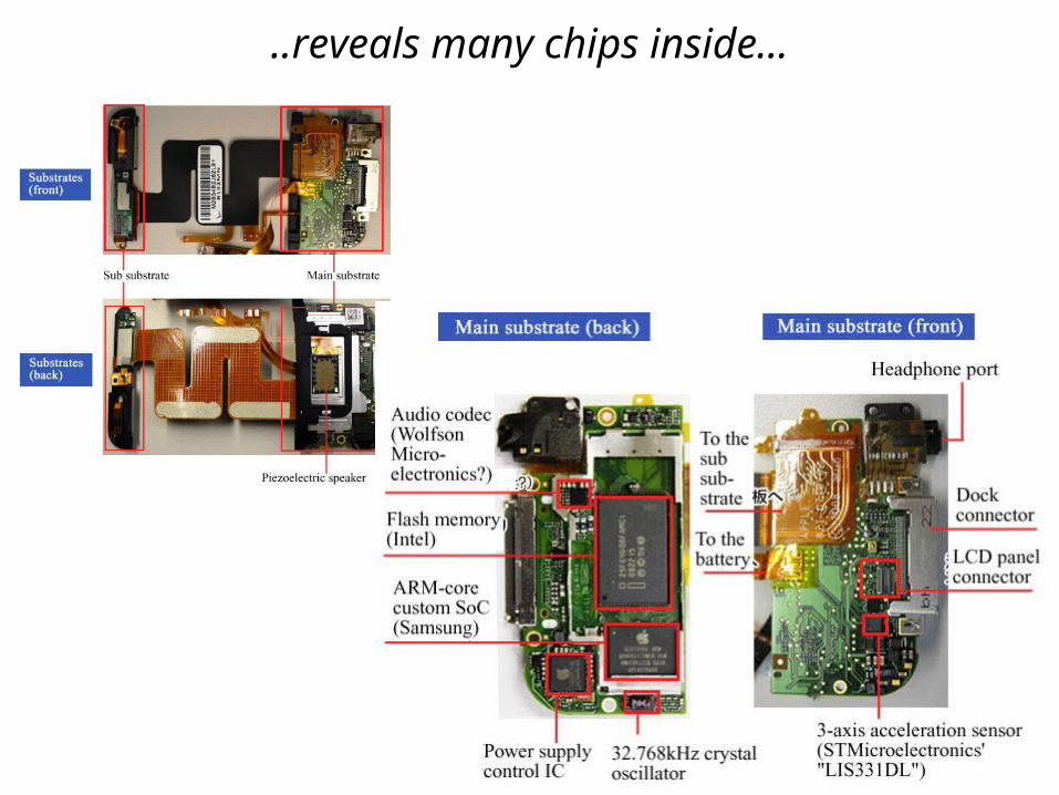
E3 237 Integrated Circuits for Wireless Communication Gaurab Banerjee Department of Electrical Communication Engineering, Indian Institute of Science, Bangalore [email protected]Lecture 1: Introduction
Transcript
E3 237 Integrated Circuits for Wireless Communication
Gaurab BanerjeeDepartment of Electrical Communication Engineering,
Tuesdays/Thursdays, 1530-1700 IST, Room 1.08 , ECE Bldg.Please be on Time!
Office hours:
To be determined after week 2 of classes, Currently by Appointment Class Mailing List:
Please send me an email with E3 237 in the subject line (follow this convention for all course related emails) to get added to the class mailing list for announcements.
Administrative Matters
Grading and Course Structure: 3 lecture-hours per week2 homework assignments (10% of course grade)Midterm (25% of course grade)Project (5% on novelty, 15% on final report, 10% on group presentation)Final Examination (35% of course grade)
TAs: TBA
Text: No textbook: Please take notes in class, or make backup arrangements.
Recommended references:
1) RF Microelectronics by B. Razavi (Pearson)2) The Design Of CMOS Radio-Frequency Integrated Circuits by T. Lee
(Cambridge University Press)
Tentative Calendar: On Class Website.
Administrative Matters
Course ContentsSystem Level Concepts:
Noise and Linearity. Concepts such as noise figure, 2-port noise parameters, IIP3. Cascaded noise figure and IIP3. The modeling of an RF system using these concepts. Receiver and Transmitter Architectures.
Circuit Design: • RLC Networks, • Low Noise Amplifiers & Mixers• Voltage Controlled Oscillators • Phase Locked Loops and Synthesizers• Power Amplifiers
Case Studies:• Cellular Transceiver• Wireless LAN transceiver• Millimeter wave transceiver
Connection to other courses
E3 284: Digital VLSI Circuits
E3 yyy: ICs for Wireline Commn.
E3 zzz: ICs for Data Conversion
E8 242: RF ICs and Systems
• Prerequisite: If you wish to take this course for credit and have not taken E3 238, you need to take my permission.
• It is recommended that students take the Digital VLSI Circuits course (Prof. Amrutur) and the RF Systems Course (Prof. Vinoy) before signing up for this course.
E3 237:ICs for Wireless Commn.
E3 238: Analog VLSI Systems
Frequencies and Applications
1 GHz 10 GHz 100 GHz Bluetooth
802.11a WLAN
UWB
GSM/CDMA
850
GSM/CDMA
1900
GPS60 GHz 802.15.3.3c
77 GHz Radar
Sub-THz imaging
• Many commercial applications span the 1-10 GHz frequency range.
• Higher f T s are pushing CMOS radios to higher frequencies, traditionally the domain of SiGe or III-V semiconductors
• Many interesting research problems, plenty of employment !!!
Cascode input stage for gain, isolation, high frequency performance
Tuned output loads
Power AmplifierMeasure signal strength and adjust pre-amp gain
Pseudo-differential cascodes
Transformer coupled, tuned output stage
Gate-biasing for optimum linearity
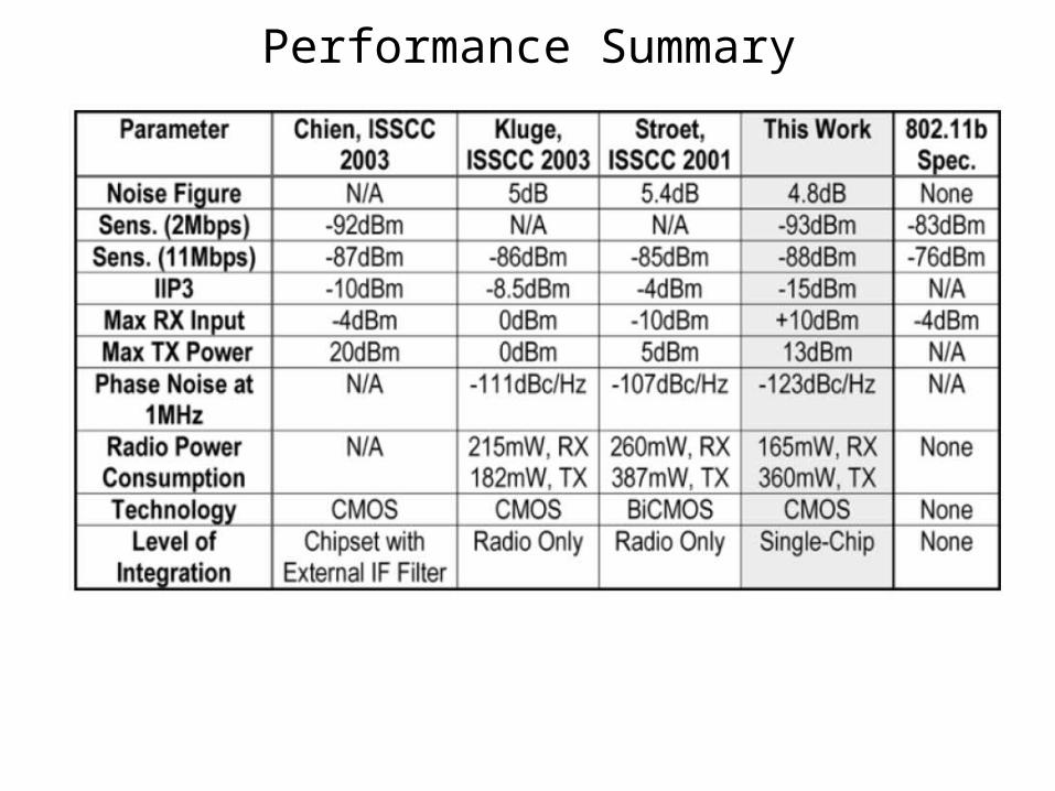
Key Transceiver Data: Receiver
Fix PER at 8% for different data rates
• RX sensitivity = -88 dBm for 11 Mbps, -93 dBm for 2 Mbps• Noise figure can be deduced from these sensitivity values
IIP3 = -15 dBm for low gain, 6 dBm for high gain
• Noise Figure dominates performance at the lower end of the dynamic range• Nonlinearities and non-ideal LO behavior dominates the higher end of the dynamic range